WO2024224495A1 - 半導体光集積素子 - Google Patents
半導体光集積素子 Download PDFInfo
- Publication number
- WO2024224495A1 WO2024224495A1 PCT/JP2023/016374 JP2023016374W WO2024224495A1 WO 2024224495 A1 WO2024224495 A1 WO 2024224495A1 JP 2023016374 W JP2023016374 W JP 2023016374W WO 2024224495 A1 WO2024224495 A1 WO 2024224495A1
- Authority
- WO
- WIPO (PCT)
- Prior art keywords
- core layer
- laser light
- optical
- section
- integrated device
- Prior art date
- Legal status (The legal status is an assumption and is not a legal conclusion. Google has not performed a legal analysis and makes no representation as to the accuracy of the status listed.)
- Ceased
Links
Images






Classifications
-
- G—PHYSICS
- G02—OPTICS
- G02B—OPTICAL ELEMENTS, SYSTEMS OR APPARATUS
- G02B6/00—Light guides; Structural details of arrangements comprising light guides and other optical elements, e.g. couplings
- G02B6/10—Light guides; Structural details of arrangements comprising light guides and other optical elements, e.g. couplings of the optical waveguide type
- G02B6/12—Light guides; Structural details of arrangements comprising light guides and other optical elements, e.g. couplings of the optical waveguide type of the integrated circuit kind
-
- G—PHYSICS
- G02—OPTICS
- G02B—OPTICAL ELEMENTS, SYSTEMS OR APPARATUS
- G02B6/00—Light guides; Structural details of arrangements comprising light guides and other optical elements, e.g. couplings
- G02B6/10—Light guides; Structural details of arrangements comprising light guides and other optical elements, e.g. couplings of the optical waveguide type
- G02B6/12—Light guides; Structural details of arrangements comprising light guides and other optical elements, e.g. couplings of the optical waveguide type of the integrated circuit kind
- G02B6/122—Basic optical elements, e.g. light-guiding paths
-
- G—PHYSICS
- G02—OPTICS
- G02B—OPTICAL ELEMENTS, SYSTEMS OR APPARATUS
- G02B6/00—Light guides; Structural details of arrangements comprising light guides and other optical elements, e.g. couplings
- G02B6/24—Coupling light guides
- G02B6/42—Coupling light guides with opto-electronic elements
-
- H—ELECTRICITY
- H01—ELECTRIC ELEMENTS
- H01S—DEVICES USING THE PROCESS OF LIGHT AMPLIFICATION BY STIMULATED EMISSION OF RADIATION [LASER] TO AMPLIFY OR GENERATE LIGHT; DEVICES USING STIMULATED EMISSION OF ELECTROMAGNETIC RADIATION IN WAVE RANGES OTHER THAN OPTICAL
- H01S5/00—Semiconductor lasers
- H01S5/02—Structural details or components not essential to laser action
- H01S5/026—Monolithically integrated components, e.g. waveguides, monitoring photo-detectors, drivers
Definitions
- This disclosure relates to a semiconductor optical integrated device.
- Patent Document 1 discloses a technology in which a non-doped layer is introduced into the optical modulator section and further the thickness of the layer is made thicker on the light incident side and thinner on the light output side, thereby reducing the concentration of optical absorption current at the light incident end face.
- Patent Document 1 aims to suppress the light absorption current by reducing the applied reverse bias voltage using a non-doped layer, and does not suppress the intensity of the light incident on the light absorption layer itself.
- an optical modulator section having a structure in which the light absorption layer is disposed near the center in the optical axis direction on the light incident end face cannot fully suppress the light absorption current near the light incident end face, and the light absorption current tends to concentrate in a small area.
- conventional semiconductor optical integrated elements have the problem that light with high intensity is incident on the light absorption layer near the light incident end face of the optical modulator section, causing the light absorption current to concentrate in a small area, which can cause deterioration of the characteristics of the semiconductor optical integrated element.
- the semiconductor optical integrated device comprises: a separation section connected to the laser diode section and having a second optical waveguide including a first core layer that propagates the laser light emitted from the laser diode section; and an optical modulator section connected to the separation section and having a third optical waveguide including a second core layer that absorbs a portion of the laser light emitted from the separation section, wherein the third optical waveguide has a constant thickness in a direction perpendicular to a surface of a substrate on which the optical modulator section is formed, and a proportion of the second core layer in a cross section of the third optical waveguide perpendicular to the laser light propagation direction increases from the incident side toward the output side of the laser light.
- the concentration of optical absorption current near the incident end face of the optical modulator section can be reduced compared to conventional techniques, making it possible to obtain a semiconductor optical integrated device in which the occurrence of characteristic degradation is suppressed.
- FIG. 1 is a schematic top view of a semiconductor optical integrated device according to a first embodiment.
- FIG. 2 is a schematic cross-sectional view of the semiconductor optical integrated device according to the first embodiment taken along the line G-G. 2 is a schematic AA cross-sectional view of the semiconductor optical integrated device according to the first embodiment.
- FIG. 2A and 2B are schematic cross-sectional views of the semiconductor optical integrated device according to the first embodiment taken along the line BB and CC, respectively.
- FIG. 2 is a schematic cross-sectional view of the semiconductor optical integrated device according to the first embodiment taken along the line DD.
- FIG. 2 is a schematic cross-sectional view taken along the line E-E of the semiconductor optical integrated device according to the first embodiment.
- FIG. 1 is a schematic cross-sectional view of a semiconductor optical integrated device according to a first embodiment taken along the line FF;
- FIG. 6 is a schematic cross-sectional view of a semiconductor optical integrated device according to a second embodiment taken along the line DD.
- FIG. 8 is a schematic cross-sectional view taken along the line E-E of a semiconductor optical integrated device according to a second embodiment.
- FIG. 11 is a schematic cross-sectional view of a semiconductor optical integrated device according to a second embodiment taken along the line G-G.
- FIG. 11 is a schematic top view showing a semiconductor optical integrated device according to a third embodiment.
- FIG. 11 is a schematic cross-sectional view of a semiconductor optical integrated device according to a third embodiment taken along the line B-B.
- FIG. 11 is a schematic cross-sectional view of a semiconductor optical integrated device according to a third embodiment taken along the line CC.
- FIG. 11 is a schematic HH cross-sectional view of a semiconductor optical integrated device according to a third embodiment.
- FIG. 11 is a schematic cross-sectional view taken along the line DD of a semiconductor optical integrated device according to a third embodiment.
- FIG. 11 is a schematic cross-sectional view taken along the line E-E of a semiconductor optical integrated device according to a third embodiment.
- FIG. 11 is a schematic cross-sectional view of a semiconductor optical integrated device according to a third embodiment taken along the line II.
- FIG. 13 is a schematic cross-sectional view taken along the line BB of the semiconductor optical integrated device according to the fourth embodiment.
- FIG. 13 is a schematic cross-sectional view of a semiconductor optical integrated device according to a fourth embodiment taken along the line CC.
- FIG. 13 is a schematic cross-sectional view taken along the line JJ of the semiconductor optical
- FIG. 1 is a schematic top view of a semiconductor optical integrated device according to the first embodiment.
- FIG. 2 is a schematic G-G cross-sectional view of the semiconductor optical integrated device according to the first embodiment shown in FIG. 1.
- FIG. 3 is a schematic A-A cross-sectional view of the semiconductor optical integrated device according to the first embodiment shown in FIG. 1.
- FIG. 4 is a schematic B-B cross-sectional view (and a schematic CC cross-sectional view) of the semiconductor optical integrated device according to the first embodiment shown in FIG. 1.
- FIG. 5 is a schematic D-D cross-sectional view of the semiconductor optical integrated device according to the first embodiment shown in FIG. 1.
- FIG. 6 is a schematic E-E cross-sectional view of the semiconductor optical integrated device according to the first embodiment shown in FIG. 1.
- FIG. 7 is a schematic F-F cross-sectional view of the optical modulator section 103 of the semiconductor optical integrated device according to the first embodiment shown in FIGS. 5 and 6.
- the semiconductor optical integrated device according to the first embodiment has a laser diode section 101 that generates laser light, an optical modulator section 103 that modulates the laser light generated from the laser diode section 101, and a separation section 102 that electrically separates the laser diode section 101 and the optical modulator section 103.
- the laser diode section 101 is configured with a structure in which an n-type InP first cladding layer 4, a laser diode section core layer 1, a p-type InP first cladding layer 6, a diffraction grating 8, and an n-type InP fourth cladding layer 9 are stacked on one side of an n-type InP substrate 12.
- the direction of the surface on which the semiconductor layers of the n-type InP substrate 12 are stacked is described as the upward direction, and the surface perpendicular to the upward direction and the propagation direction of the laser light is described as the side.
- the semiconductor burying layer 13 may be composed of p-type InP and n-type InP, or may use a semiconductor such as Fe-doped InP.
- a p-type first contact layer 10 is laminated on the upper surface of the n-type InP fourth cladding layer 9 and the semiconductor burying layer 13, and a protective passivation film 14 is formed on the upper surface of the p-type first contact layer 10.
- an electrode 16 which is an anode electrode, is formed on the protective passivation film 14, and the electrode 16 and the p-type first contact layer 10 are electrically connected through an opening formed in the protective passivation film 14.
- the separation section 102 is configured with a structure in which an n-type InP second cladding layer 5, a first waveguide core layer 2, and a p-type InP second cladding layer 7 are stacked on an n-type InP substrate 12.
- the second optical waveguide 21 shown in Figure 1 refers to an optical waveguide including an n-type InP second cladding layer 5, a first waveguide core layer 2, and a p-type InP second cladding layer 7. Both side portions of the first waveguide core layer 2 are embedded with a semiconductor burying layer 13 to form an embedded structure.
- a p-type first contact layer 10 is stacked on the upper surfaces of the p-type InP second cladding layer 7 and the semiconductor burying layer 13, and a protective passivation film 14 is formed on the upper surface of the p-type first contact layer 10.
- a first electrode 11, which is a cathode electrode, is provided on the lower surface, which is the other surface of the n-type InP substrate 12.
- the second optical waveguide may have a high mesa ridge structure.
- the optical modulator section 103 is configured with a structure in which an n-type InP second cladding layer 5, an optical modulator section core layer 3 and a first waveguide core layer 2, and a p-type InP second cladding layer 7 are laminated on an n-type InP substrate 12.
- the third optical waveguide 22 shown in Figure 1 refers to an optical waveguide including an n-type InP second cladding layer 5, an optical modulator section core layer 3 and a first waveguide core layer 2, and a p-type InP second cladding layer 7. Both side portions of the third optical waveguide 22, like both side portions of the first waveguide core layer 2, have a buried structure buried by a semiconductor burying layer 13.
- a p-type first contact layer 10 is laminated on the upper surfaces of the p-type InP second cladding layer 7 and the semiconductor burying layer 13, and a protective passivation film 14 is formed on the upper surface of the p-type first contact layer 10. Furthermore, an electrode 16, which is an anode electrode, is formed on the protective passivation film 14, and the electrode 17 and the p-type first contact layer 10 are electrically connected through an opening formed in the protective passivation film 14.
- a first electrode 11 is provided on the lower surface side of the n-type InP substrate 12 and is electrically connected to the n-type InP substrate 12.
- the third optical waveguide 22 may have a high mesa ridge structure. As shown in FIG.
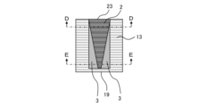
- the optical modulator section 103 has a structure in which the distance between the side surfaces of the first waveguide core layer 2, that is, the width of the first waveguide core layer 2 in the traveling direction of the laser light, narrows from the laser light incident side connected to the separation section 102 toward the laser light output end face 19 side.
- the width of the third optical waveguide 22 in the traveling direction of the laser light is constant, the width of the optical modulator section core layer 3 widens toward the traveling direction of the laser light in response to the narrowing of the width of the first waveguide core layer 2 in the traveling direction of the laser light.
- the width of the first waveguide core layer 2 narrows continuously from the laser light incident side toward the laser light output end face 19 side, but it may be formed in a stepped staircase shape, or may be a combination of a continuous structure and a stepped structure.
- the laser diode section 101 is configured, for example, with a distributed feedback laser structure.
- the distributed feedback laser structure is provided with a diffraction grating 8, which allows single-mode oscillation of laser light to be obtained.
- the optical modulator section 103 is an electroabsorption modulator that controls the amount of light absorption by an electric field, and the amount of light absorption increases when a reverse bias voltage is applied. In other words, the input laser light is modulated depending on the magnitude of the voltage applied to the optical modulator section 103. When light is absorbed, the absorbed light is converted into carriers, and a current flows as a photocurrent.
- the optical absorption current is concentrated near the incident end face of the optical modulator section where the optical intensity is the highest, it is possible to suppress the optical absorption current from concentrating in a minute region by reducing the amount of light absorption near the incident end face of the optical modulator section. Specifically, it is conceivable to reduce the intensity of light incident on the optical modulator section core layer where optical absorption occurs at the incident end face of the optical modulator section where the optical intensity is high.
- the amount of light absorbed at a certain x also exponentially decreases from the input end of the optical waveguide toward the output direction. Therefore, in the optical waveguide of an electroabsorption (EA) modulator, by making ⁇ small on the input side where the light intensity is high and making ⁇ continuously large toward the output side, it is possible to reduce the light absorption current on the input side where the light intensity is high. This makes it possible to approach the direction in which the amount of light absorbed per unit area is averaged in the optical axis direction, and the increase in the light absorption current density on the input side can be suppressed compared to the conventional method.
- EA electroabsorption
- the third optical waveguide 22 of the optical modulator section 103 has both side portions of the first waveguide core layer 2, which does not function as an optical absorption layer, embedded with the optical modulator section core layer 3, which functions as an optical absorption layer, as shown in Figs. 5, 6 and 7.
- the ratio of the cross-sectional area of the optical modulator section core layer 3 increases from the light incident side to the light exit side.
- the ratio of the light incident on the third optical waveguide 22 that is applied to the optical modulator section core layer 3 increases from the light incident side to the light exit side, which means that the substantial optical confinement factor ⁇ of the third optical waveguide 22 increases from the light incident side to the light exit side. Since the amount of light absorption is correlated with the optical confinement factor ⁇ , in the third optical waveguide 22 configured in this manner, the amount of light absorption on the incident end face 23 side can be suppressed compared to the light exit end face side while keeping the thickness of the third optical waveguide 22 constant.
- the term "keep the thickness constant" used here means that the thickness does not have to be changed as a design intent.
- the thickness is strictly constant, but includes the case where the thickness is approximately constant.
- the total width of the first waveguide core layer 2 and the optical modulator core layer 3 is about 2 ⁇ m
- the width of the first waveguide core layer 2 on the side of the incident end face 23 is about 2 ⁇ m
- the width of the first waveguide core layer 2 on the side of the exit end face is about 0.4 ⁇ m.
- the width of the first waveguide core layer 2 of the optical modulator section 103 may be not only a tapered shape that narrows continuously from the light incident side to the light emitting side, but also a stepped shape that narrows in a stepped manner.
- the first waveguide core layer 2 of the optical modulator section 103 may be extended to the end face of the semiconductor optical integrated device.
- the first waveguide core layer 2 of the optical modulator section 103 may be grown together with the optical waveguide layer of the separation section 102, or may be grown separately.
- the semiconductor buried layer 13 may be made of p-type InP and n-type InP, or may use a semiconductor such as Fe-doped InP.
- the laser diode section core layer 1 of the laser diode section 101 is made of, for example, an InGaAsP-based multiple quantum well layer, and the band gap wavelength of the multiple quantum well layer is about 1.2 to 1.6 ⁇ m.
- the band gap wavelength of the first waveguide core layer 2 of the separation section 102 and the optical modulator section 103 may be set to be shorter than the laser wavelength oscillated from the laser diode section 101, for example, about 0.9 to 1.5 ⁇ m.
- the band gap wavelength of the optical modulator section core layer 3 of the optical modulator section 103 may be set to be shorter than the laser wavelength oscillated from the laser diode section 101, for example, a band gap wavelength of about 0.9 to 1.5 ⁇ m composed of an InGaAsP-based multiple quantum well layer.
- the band gap wavelength of the optical modulator section core layer 3 may be constant from the light incident side toward the light emitting side, or may be lengthened continuously or stepwise.
- the laser diode section core layer 1 and the optical modulator section core layer 3 may be formed by applying a selective growth technique, or may be formed separately by Butt-Joint growth.
- an n-type InP first cladding layer 4 In the region where the laser diode section 101 is formed, an n-type InP first cladding layer 4, a laser diode section core layer 1, a p-type InP first cladding layer 6, a diffraction grating 8, and an n-type InP fourth cladding layer 9 are laminated on an n-type InP substrate 12.
- an n-type InP second cladding layer 5 and a first waveguide core layer 2 are laminated on an n-type InP substrate 12.
- an insulating film is formed on the upper surface of the first waveguide core layer 2, and the insulating film is patterned so that the insulating film remains in a shape corresponding to the first waveguide core layer 2 shown in FIG. 7.
- the first waveguide core layer 2 of the optical modulator section 103 is etched using an etching technique such as dry etching to form a first waveguide core layer 2 having a shape shown in FIG. 7.
- both side portions of the first waveguide core layer 2 of the optical modulator section 103 are embedded with the optical modulator section core layer 3.
- the insulating film used as an etching mask is removed, and the separation section 102 and the p-type InP second cladding layer 7 of the optical modulator section 103 are laminated.
- an insulating film is formed on the upper surfaces of the n-type InP fourth cladding layer 9 of the laser diode section 101, the p-type InP second cladding layer 7 of the separation section 102, and the p-type InP second cladding layer 7 of the optical modulator section 103, and the insulating film is patterned into shapes corresponding to the ridge structures of the first optical waveguide 20, the second optical waveguide 21, and the third optical waveguide 22, respectively.
- the ridge structures of the first optical waveguide 20, the second optical waveguide 21, and the third optical waveguide 22 are formed by using an etching technique such as dry etching.
- an etching technique such as dry etching.
- both side portions of the ridge structure of the laser diode section 101, the separation section 102, and the optical modulator section 103 are buried with a semiconductor burying layer 13.
- the semiconductor burying layer 13 may be composed of p-type InP and n-type InP, or a semiconductor such as Fe-doped InP may be used.
- the insulating film is removed, and the p-type first contact layer 10 is laminated.
- a protective passivation film 14 is formed on the upper surface of the p-type first contact layer 10.
- An opening is formed in the protective passivation film 14 on the upper surface of the laser diode section 101, and an electrode 16 electrically connected to the p-type first contact layer 10 is formed. Also, an opening is formed in the protective passivation film 14 on the upper surface of the optical modulator section 103, and an electrode 17 electrically connected to the p-type first contact layer 10 and a bonding pad 18 electrically connected to the electrode 17 are formed.
- the semiconductor optical integrated device has a structure in which the thickness of the third optical waveguide 22 of the optical modulator section 103 is constant, while both side surfaces of the first waveguide core layer 2, which does not function as an optical absorption layer, are embedded with the optical modulator section core layer 3, which functions as an optical absorption layer.
- the optical modulator section core layer 3 is provided at a position sandwiching the first waveguide core layer 2 from the sides in the propagation direction of the laser light.
- the ratio of the cross-sectional area of the optical modulator section core layer 3 to the vertical cross section of the third optical waveguide 22 relative to the optical axis increases from the incident side to the exit side of the light.
- the semiconductor optical integrated device configured in this manner can suppress the amount of light absorption on the light incident end face 23 side compared to the light emitting end face 19 side, while keeping the thickness of the third optical waveguide 22 constant.
- the semiconductor optical integrated element shown in the first embodiment it is possible to prevent light with high intensity from being incident on the optical absorption layer near the incident end face 23 of the optical modulator section, and therefore it is possible to provide a semiconductor optical integrated element that prevents the deterioration of characteristics caused by the optical absorption current concentrating in a small area.
- Embodiment 2 The semiconductor optical integrated device according to the second embodiment is described below. Since the configuration of the semiconductor optical integrated device according to the second embodiment is the same as that of the first embodiment except for the structure of the optical modulator section 103, the following mainly describes the differences from the first embodiment, and may omit overlapping parts.
- FIG. 8 is a schematic DD cross-sectional view of the semiconductor optical integrated device according to the second embodiment shown in Fig. 1.
- Fig. 9 is a schematic EE cross-sectional view of the semiconductor optical integrated device according to the second embodiment shown in Fig. 1.
- Fig. 10 is a schematic GG cross-sectional view of the optical modulator section 103 of the semiconductor optical integrated device according to the second embodiment shown in Fig. 1.
- the optical modulator section 103 of the semiconductor optical integrated device according to the second embodiment is configured to have a structure in which an n-type InP second cladding layer 5, a first waveguide core layer 2, an optical modulator section core layer 3, and a p-type InP second cladding layer 7 are laminated on an n-type InP substrate 12.
- the first waveguide core layer 2 has a structure in which the thickness in the lamination direction of the third optical waveguide 22, that is, the thickness in the vertical direction, is continuously reduced from the laser light incident side toward the laser light output end face 19 side.
- the thickness of the optical modulator section core layer 3 is structured to be thicker toward the laser light traveling direction in response to the thickness of the first waveguide core layer 2 being thinner in the laser light traveling direction.
- the thickness of the first waveguide core layer 2 and the optical modulator core layer 3 is shown to change continuously along the traveling direction of the laser light, they may be formed in a stepped shape, or may be a combination of a continuous structure and a stepped structure. Also, the order of laminating the first waveguide core layer 2 and the optical modulator core layer 3 may be reversed.
- the semiconductor optical integrated device has a structure in which the first waveguide core layer 2, which does not function as a light absorption layer, and the optical modulator core layer 3 are stacked in the vertical direction while the thickness of the third optical waveguide 22 of the optical modulator section 103 is constant. Furthermore, the thickness of the optical modulator core layer 3 increases in the traveling direction of the laser light. In other words, the ratio of the cross-sectional area of the optical modulator core layer 3 to the vertical cross section of the third optical waveguide 22 relative to the optical axis increases from the incident side toward the exit side of the light.
- the semiconductor optical integrated device configured in this manner can suppress the amount of light absorption on the light incident end face 23 side compared to the light emitting end face 19 side, while keeping the thickness of the third optical waveguide 22 constant.
- the semiconductor optical integrated element shown in the second embodiment it is possible to prevent light with high intensity from being incident on the optical absorption layer near the incident end face 23 of the optical modulator section, as in the first embodiment, and therefore it is possible to provide a semiconductor optical integrated element that prevents the deterioration of characteristics caused by the optical absorption current concentrating in a small area.
- Embodiment 3 The semiconductor optical integrated device according to the third embodiment is described below.
- the configuration of the semiconductor optical integrated device according to the third embodiment is different from that of the first embodiment in the structures of the separation section 102 and the optical modulator section 103. Differences from the first embodiment are mainly described, and overlapping parts may be omitted.
- FIG. 11 is a schematic top view showing a semiconductor optical integrated device according to the third embodiment.
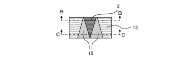
- FIG. 12 is a schematic cross-sectional view taken along line B-B of the separation unit 102 shown in FIG. 11 of the semiconductor optical integrated device according to the third embodiment.
- FIG. 13 is a schematic cross-sectional view taken along line C-C of the separation unit 102 shown in FIG. 11 of the semiconductor optical integrated device according to the third embodiment.
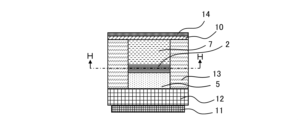
- FIG. 14 is a schematic cross-sectional view taken along line H-H of the separation unit 102 shown in FIG. 12 and FIG. 13 of the semiconductor optical integrated device according to the third embodiment.
- FIG. 15 is a schematic cross-sectional view taken along line D-D of the optical modulator unit 103 shown in FIG. 11 of the semiconductor optical integrated device according to the third embodiment.
- FIG. 16 is a schematic cross-sectional view taken along line E-E of the optical modulator unit 103 shown in FIG. 11 of the semiconductor optical integrated device according to the third embodiment.
- FIG. 17 is a schematic cross-sectional view taken along line I-I of the optical modulator unit 103 shown in FIG. 15 and FIG. 16 of the semiconductor optical integrated device according to the third embodiment.
- the separation section 102 of the semiconductor optical integrated device according to the third embodiment has a structure in which the width of the second optical waveguide 21 in the laser light traveling direction becomes wider toward the laser light traveling direction. Also, as shown in Fig. 15 to Fig.
- the optical modulator section 103 of the semiconductor optical integrated device has a structure in which the width of the third optical waveguide 22 in the laser light traveling direction becomes narrower toward the laser light traveling direction.
- the third optical waveguide 22 has a constant height, and an optical modulator section core layer 3 with a constant width is formed in the center along the laser light traveling direction, and both side surfaces of the optical modulator section core layer 3 are embedded with the first waveguide core layer 2.
- the width of the first waveguide core layer 2 embedded in both side surfaces of the optical modulator section core layer 3 becomes narrower along the laser light traveling direction.
- the width of the first waveguide core layer 2 is shown to be continuously narrowed along the traveling direction of the laser light, but it may be formed in a stepped shape having steps, or may be a combination of a continuous structure and a stepped structure.
- the width of the second optical waveguide 21 of the separation section 102 becomes wider from the light incident side toward the light exit side.
- the optical confinement factor ⁇ at the incident end face 23 of the optical modulator section 103 can be reduced, and the optical intensity per unit area can be reduced.
- the width of the first waveguide core layer 2 of the optical modulator section 103 becomes narrower from the light incident side toward the light exit side.
- the optical confinement factor ⁇ of the optical modulator section core layer 3 can be increased from the light incident side toward the light exit side.
- the laser light can be reduced in intensity by passing through the separation section 102, and further, in the optical modulator section 103, the amount of light absorption on the incident end face 23 side can be suppressed compared to the light exit end face 19 side.
- the concentration of the optical absorption current in the vicinity of the incident end face 23 of the optical modulator section 103 can be reduced compared to the conventional semiconductor optical integrated device.
- the width of the second optical waveguide 21 of the separation section 102 becomes wider from the light incident side toward the light exit side. Furthermore, the width of the first waveguide core layer 2 of the optical modulator section 103 becomes narrower from the light incident side toward the light exit side, and the ratio of the cross-sectional area of the optical modulator section core layer 3 to the vertical cross section of the third optical waveguide 22 relative to the optical axis becomes larger from the light incident side toward the light exit side.
- the semiconductor optical integrated device configured in this manner can suppress the amount of light absorption on the light incident end face 23 side compared to the light emitting end face 19 side, while keeping the thickness of the third optical waveguide 22 constant.
- the semiconductor optical integrated element shown in the third embodiment it is possible to prevent light with high intensity from being incident on the optical absorption layer near the incident end face 23 of the optical modulator section, as in the first embodiment, and therefore it is possible to provide a semiconductor optical integrated element that prevents the deterioration of characteristics caused by the optical absorption current concentrating in a small area.
- Embodiment 4 The semiconductor optical integrated device according to the fourth embodiment is described below. Since the configuration of the semiconductor optical integrated device according to the fourth embodiment is the same as that of the third embodiment except for the structure of the separation unit 102, the following mainly describes the differences from the third embodiment, and may omit overlapping portions.
- FIG. 11 A schematic top view of the semiconductor optical integrated device according to the fourth embodiment is similar to Fig. 11.
- Fig. 18 is a schematic cross-sectional view taken along line B-B of the separation unit 102 shown in Fig. 11 of the semiconductor optical integrated device according to the fourth embodiment.
- Fig. 19 is a schematic cross-sectional view taken along line CC of the separation unit 102 shown in Fig. 11 of the semiconductor optical integrated device according to the fourth embodiment.
- Fig. 20 is a schematic cross-sectional view taken along line J-J of the separation unit 102 shown in Figs. 18 and 19 of the semiconductor optical integrated device according to the fourth embodiment.
- the separation section 102 is configured to have a structure in which an n-type InP second cladding layer 5, a first waveguide core layer 2 and a second waveguide core layer 15, and a p-type InP second cladding layer 7 are laminated on an n-type InP substrate 12.
- a first electrode 11 serving as a cathode electrode is provided on the lower surface of the n-type InP substrate 12, and the first electrode 11 and the n-type InP substrate 12 are electrically connected.
- the second optical waveguide 21 shown in FIG. 11 indicates an optical waveguide including the n-type InP second cladding layer 5, the first waveguide core layer 2 and the second waveguide core layer 15, and the p-type InP second cladding layer 7.
- the width of the first waveguide core layer 2 of the separation section 102 is continuously narrowed from the incident side to the output side of the laser light.
- the width of the first waveguide core layer 2 of the separation section 102 may be a stepped shape having a step-like narrowing shape, instead of a tapered shape having a step-like narrowing shape from the incident side to the output side of the light.
- the width of the second waveguide core layer 15 of the separation section 102 is continuously widened.
- the width of the second waveguide core layer 15 may be a stepped shape having a step-like widening shape, instead of an inverse tapered shape having a step-like widening shape from the incident side to the output side of the light.
- the semiconductor constituting the first waveguide core layer 2 and the semiconductor constituting the second waveguide core layer 15 are semiconductors having different band gap wavelengths, so that the beam diameter of the laser light passing through the second optical waveguide 21 can be controlled.
- the first waveguide core layer 2 is made of an InGaAsP-based material with a bandgap wavelength of about 0.9 to 1.5 ⁇ m
- the second waveguide core layer 15 is made of an InP-based material with a bandgap wavelength of about 0.9 to 1.0 ⁇ m, so that the spread and coupling of the laser light can be changed.
- the width of the second optical waveguide 21 of the separation section 102 is wider from the light incident side toward the light exit side, as in the fourth embodiment.
- the width of the first waveguide core layer 2 of the separation section 102 narrows from the incident side to the output side of the laser light, and the width of the second waveguide core layer 15 continuously widens.
- the semiconductors constituting the first waveguide core layer 2 and the semiconductors constituting the second waveguide core layer 15 are semiconductors having different band gap wavelengths. This makes it possible to couple the laser light more efficiently than in the third embodiment and make it incident on the optical modulator section 103.
- the width of the first waveguide core layer 2 of the optical modulator section 103 narrows from the incident side to the output side of the light, and the ratio of the cross-sectional area of the optical modulator section core layer 3 to the vertical cross section of the third optical waveguide 22 relative to the optical axis increases from the incident side to the output side of the light.
- the semiconductor optical integrated device configured in this manner can suppress the amount of light absorption on the light incident end face 23 side compared to the light emitting end face 19 side while keeping the thickness of the third optical waveguide 22 constant, and can couple laser light more efficiently than in the third embodiment.
- the semiconductor optical integrated element shown in the fourth embodiment as in the third embodiment, it is possible to prevent light with high intensity from being incident on the optical absorption layer near the incident end face 23 of the optical modulator section, thereby preventing deterioration of characteristics caused by the optical absorption current concentrating in a small area, and further providing a semiconductor optical integrated element capable of efficient coupling of laser light.
- Laser diode section core layer 2 First waveguide core layer 3
- Optical modulator section core layer 4 n-type InP first cladding layer 5 n-type InP second cladding layer 6 p-type InP first cladding layer 7 p-type InP second cladding layer 8 Diffraction grating 9 n-type InP fourth cladding layer 10 p-type first contact layer 11 First electrode 12 n-type InP substrate 13 Semiconductor buried layer 14 Protective passivation film 15 Second waveguide core layer 16 Electrode 17 Electrode 18 Bonding pad 19 Emission end surface 20 First optical waveguide 21 Second optical waveguide 22 Third optical waveguide 23 Incident end surface 101 Laser diode section 102 Separation section 103 Optical modulator section
Landscapes
- Physics & Mathematics (AREA)
- General Physics & Mathematics (AREA)
- Optics & Photonics (AREA)
- Engineering & Computer Science (AREA)
- Microelectronics & Electronic Packaging (AREA)
- Condensed Matter Physics & Semiconductors (AREA)
- Electromagnetism (AREA)
- Semiconductor Lasers (AREA)
- Optical Integrated Circuits (AREA)
- Optical Modulation, Optical Deflection, Nonlinear Optics, Optical Demodulation, Optical Logic Elements (AREA)
Priority Applications (3)
| Application Number | Priority Date | Filing Date | Title |
|---|---|---|---|
| CN202380096541.6A CN121039543A (zh) | 2023-04-26 | 2023-04-26 | 半导体光集成元件 |
| PCT/JP2023/016374 WO2024224495A1 (ja) | 2023-04-26 | 2023-04-26 | 半導体光集積素子 |
| JP2024515102A JP7501819B1 (ja) | 2023-04-26 | 2023-04-26 | 半導体光集積素子 |
Applications Claiming Priority (1)
| Application Number | Priority Date | Filing Date | Title |
|---|---|---|---|
| PCT/JP2023/016374 WO2024224495A1 (ja) | 2023-04-26 | 2023-04-26 | 半導体光集積素子 |
Publications (1)
| Publication Number | Publication Date |
|---|---|
| WO2024224495A1 true WO2024224495A1 (ja) | 2024-10-31 |
Family
ID=91483412
Family Applications (1)
| Application Number | Title | Priority Date | Filing Date |
|---|---|---|---|
| PCT/JP2023/016374 Ceased WO2024224495A1 (ja) | 2023-04-26 | 2023-04-26 | 半導体光集積素子 |
Country Status (3)
| Country | Link |
|---|---|
| JP (1) | JP7501819B1 (https=) |
| CN (1) | CN121039543A (https=) |
| WO (1) | WO2024224495A1 (https=) |
Families Citing this family (2)
| Publication number | Priority date | Publication date | Assignee | Title |
|---|---|---|---|---|
| JP7648836B1 (ja) | 2024-06-26 | 2025-03-18 | 三菱電機株式会社 | 光変調器集積半導体レーザ、光変調器集積半導体レーザの駆動方法、光モジュール、多値強度変調送受信装置、及び光回線終端装置 |
| JP7802250B1 (ja) * | 2025-03-13 | 2026-01-19 | 三菱電機株式会社 | 光変調器集積半導体レーザ及び光モジュール |
Citations (8)
| Publication number | Priority date | Publication date | Assignee | Title |
|---|---|---|---|---|
| JPH01217418A (ja) * | 1988-02-26 | 1989-08-31 | Kokusai Denshin Denwa Co Ltd <Kdd> | 光変調素子 |
| JP2002527793A (ja) * | 1998-10-15 | 2002-08-27 | テレフオンアクチーボラゲツト エル エム エリクソン | 電界効果光吸収変調器とその製造法 |
| JP2011076054A (ja) * | 2009-09-02 | 2011-04-14 | Fujikura Ltd | 光学素子 |
| US20140376577A1 (en) * | 2013-02-19 | 2014-12-25 | Mark HEIMBUCH | Variable bandgap modulator for a modulated laser system |
| US20170179679A1 (en) * | 2015-12-16 | 2017-06-22 | Electronics And Telecommunications Research Institute | Semiconductor optical device |
| WO2018134940A1 (ja) * | 2017-01-19 | 2018-07-26 | 三菱電機株式会社 | 光変調器集積半導体レーザ |
| WO2020224775A1 (en) * | 2019-05-08 | 2020-11-12 | Huawei Technologies Co., Ltd. | Compound optical device |
| WO2021059449A1 (ja) * | 2019-09-26 | 2021-04-01 | 日本電信電話株式会社 | 光送信器 |
-
2023
- 2023-04-26 JP JP2024515102A patent/JP7501819B1/ja active Active
- 2023-04-26 CN CN202380096541.6A patent/CN121039543A/zh active Pending
- 2023-04-26 WO PCT/JP2023/016374 patent/WO2024224495A1/ja not_active Ceased
Patent Citations (8)
| Publication number | Priority date | Publication date | Assignee | Title |
|---|---|---|---|---|
| JPH01217418A (ja) * | 1988-02-26 | 1989-08-31 | Kokusai Denshin Denwa Co Ltd <Kdd> | 光変調素子 |
| JP2002527793A (ja) * | 1998-10-15 | 2002-08-27 | テレフオンアクチーボラゲツト エル エム エリクソン | 電界効果光吸収変調器とその製造法 |
| JP2011076054A (ja) * | 2009-09-02 | 2011-04-14 | Fujikura Ltd | 光学素子 |
| US20140376577A1 (en) * | 2013-02-19 | 2014-12-25 | Mark HEIMBUCH | Variable bandgap modulator for a modulated laser system |
| US20170179679A1 (en) * | 2015-12-16 | 2017-06-22 | Electronics And Telecommunications Research Institute | Semiconductor optical device |
| WO2018134940A1 (ja) * | 2017-01-19 | 2018-07-26 | 三菱電機株式会社 | 光変調器集積半導体レーザ |
| WO2020224775A1 (en) * | 2019-05-08 | 2020-11-12 | Huawei Technologies Co., Ltd. | Compound optical device |
| WO2021059449A1 (ja) * | 2019-09-26 | 2021-04-01 | 日本電信電話株式会社 | 光送信器 |
Also Published As
| Publication number | Publication date |
|---|---|
| JP7501819B1 (ja) | 2024-06-18 |
| CN121039543A (zh) | 2025-11-28 |
| JPWO2024224495A1 (https=) | 2024-10-31 |
Similar Documents
| Publication | Publication Date | Title |
|---|---|---|
| JP5638483B2 (ja) | 半導体レーザ装置 | |
| JP5387671B2 (ja) | 半導体レーザ及び集積素子 | |
| EP0641049B1 (en) | An optical semiconductor device and a method of manufacturing the same | |
| JP4952376B2 (ja) | 光導波路と半導体光集積素子の製造方法 | |
| JP7501819B1 (ja) | 半導体光集積素子 | |
| JP6825251B2 (ja) | 発光素子 | |
| JP6790529B2 (ja) | 発光デバイス | |
| JP2008135786A (ja) | 高出力半導体レーザダイオード | |
| US20080042122A1 (en) | Semiconductor light emitting element, method of manufacturing the same and semiconductor light emitting device | |
| JP2018026478A (ja) | 発光素子、発光素子アレイ、及び光伝送装置 | |
| CN114365359B (zh) | 半导体激光装置 | |
| JP3525257B1 (ja) | 半導体発光素子 | |
| US12531391B2 (en) | Semiconductor optical integrated element | |
| JP2007243072A (ja) | 半導体光増幅器複合半導体レーザー装置 | |
| TWI717954B (zh) | 光半導體積體元件 | |
| JP4014861B2 (ja) | 化合物半導体デバイス及びその作製方法 | |
| JP5957856B2 (ja) | 半導体集積素子 | |
| US12158609B2 (en) | Semiconductor optical device and method for manufacturing the same | |
| JP2001024211A (ja) | 半導体受光素子 | |
| JP7475561B1 (ja) | 光半導体集積装置 | |
| JP2000252579A (ja) | 半導体光素子及びその製造方法 | |
| JP3691507B2 (ja) | 半導体レーザ | |
| WO2026022890A1 (ja) | 光半導体素子 | |
| WO2025186867A1 (ja) | 半導体光素子 | |
| JP2001142036A (ja) | 半導体光変調器およびその製造方法 |
Legal Events
| Date | Code | Title | Description |
|---|---|---|---|
| WWE | Wipo information: entry into national phase |
Ref document number: 2024515102 Country of ref document: JP |
|
| 121 | Ep: the epo has been informed by wipo that ep was designated in this application |
Ref document number: 23935275 Country of ref document: EP Kind code of ref document: A1 |
|
| NENP | Non-entry into the national phase |
Ref country code: DE |
|
| 122 | Ep: pct application non-entry in european phase |
Ref document number: 23935275 Country of ref document: EP Kind code of ref document: A1 |