WO2024214257A1 - 駆動回路 - Google Patents
駆動回路 Download PDFInfo
- Publication number
- WO2024214257A1 WO2024214257A1 PCT/JP2023/015069 JP2023015069W WO2024214257A1 WO 2024214257 A1 WO2024214257 A1 WO 2024214257A1 JP 2023015069 W JP2023015069 W JP 2023015069W WO 2024214257 A1 WO2024214257 A1 WO 2024214257A1
- Authority
- WO
- WIPO (PCT)
- Prior art keywords
- circuit
- power semiconductor
- igbt
- igbts
- detection
- Prior art date
- Legal status (The legal status is an assumption and is not a legal conclusion. Google has not performed a legal analysis and makes no representation as to the accuracy of the status listed.)
- Ceased
Links
Images


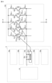
Classifications
-
- H—ELECTRICITY
- H02—GENERATION; CONVERSION OR DISTRIBUTION OF ELECTRIC POWER
- H02M—APPARATUS FOR CONVERSION BETWEEN AC AND AC, BETWEEN AC AND DC, OR BETWEEN DC AND DC, AND FOR USE WITH MAINS OR SIMILAR POWER SUPPLY SYSTEMS; CONVERSION OF DC OR AC INPUT POWER INTO SURGE OUTPUT POWER; CONTROL OR REGULATION THEREOF
- H02M1/00—Details of apparatus for conversion
-
- H—ELECTRICITY
- H02—GENERATION; CONVERSION OR DISTRIBUTION OF ELECTRIC POWER
- H02M—APPARATUS FOR CONVERSION BETWEEN AC AND AC, BETWEEN AC AND DC, OR BETWEEN DC AND DC, AND FOR USE WITH MAINS OR SIMILAR POWER SUPPLY SYSTEMS; CONVERSION OF DC OR AC INPUT POWER INTO SURGE OUTPUT POWER; CONTROL OR REGULATION THEREOF
- H02M1/00—Details of apparatus for conversion
- H02M1/08—Circuits specially adapted for the generation of control voltages for semiconductor devices incorporated in static converters
-
- H—ELECTRICITY
- H03—ELECTRONIC CIRCUITRY
- H03K—PULSE TECHNIQUE
- H03K17/00—Electronic switching or gating, i.e. not by contact-making and –breaking
- H03K17/08—Modifications for protecting switching circuit against overcurrent or overvoltage
-
- H—ELECTRICITY
- H03—ELECTRONIC CIRCUITRY
- H03K—PULSE TECHNIQUE
- H03K17/00—Electronic switching or gating, i.e. not by contact-making and –breaking
- H03K17/12—Modifications for increasing the maximum permissible switched current
Definitions
- This disclosure relates to a drive circuit, and more specifically to a drive circuit for driving multiple power semiconductor devices connected in parallel.
- IGBTs insulated gate bipolar transistors
- MOSFETs metal-oxide-semiconductor field-effect transistors
- a drive circuit that drives multiple power semiconductor elements connected in parallel requires a function that detects an overcurrent or short circuit state of the power semiconductor elements and protects the power semiconductor elements from thermal destruction.
- Driving circuits equipped with such a short-circuit protection function are known, for example, from JP 2021-044963 A (Patent Document 1) and JP 2000-217337 A (Patent Document 2).
- the "gate drive device for driving multiple insulated gate semiconductor elements connected in parallel” disclosed in JP 2021-044963 A includes a gate drive circuit that drives the gates of the multiple insulated gate semiconductor elements in response to a control signal provided from the outside, an abnormality detection circuit that includes multiple abnormality detection terminals corresponding to each of the multiple insulated gate semiconductor elements and detects an abnormal state of the multiple insulated gate semiconductor elements and outputs an abnormality detection signal, and an output circuit that is connected to at least one of the multiple abnormality detection terminals and outputs the abnormality detection signal to the outside” (see claim 1 of Patent Document 1).
- Patent Document 2 the semiconductor device disclosed in JP 2000-217337 A (Patent Document 2) is "configured so that a plurality of voltage-driven elements are divided into a plurality of groups each consisting of a parallel connection of a plurality of voltage-driven elements including a voltage-driven element having an auxiliary emitter for current detection, and each of these groups is protected from overcurrent by one overcurrent protection circuit.” And, “within each group, the auxiliary emitter, main emitter and gate of the voltage-driven element with the largest collector current at the same gate-emitter voltage are connected to the overcurrent protection circuit" (see claims 1 and 2 of Patent Document 2).
- an abnormality detection terminal is provided corresponding to each of the multiple semiconductor elements connected in parallel, and the current flowing through the detection resistor connected to the sense emitter of each semiconductor element is detected.
- the abnormality detection circuit tends to become large and complex.
- Patent Document 2 the current flowing through the detection resistor connected to the auxiliary emitter of the semiconductor element "within each group, the collector current is the largest at the same gate-emitter voltage" is detected.
- the collector current is usually designed to be uniform, it is unrealistic to identify the semiconductor element with the largest collector current at the design stage and connect its auxiliary emitter, main emitter, and gate to an overcurrent protection circuit.
- the present disclosure has been made in consideration of the above-mentioned background art, and its purpose is to provide a drive circuit with a short-circuit protection function that detects, with a simple configuration, a short-circuit state that occurs in any of multiple power semiconductor elements connected in parallel, and protects these power semiconductor elements.
- a drive circuit for driving a plurality of power semiconductor elements connected in parallel to one another includes a common substrate and a plurality of individual substrates.
- the common substrate generates a common drive signal for controlling the on and off of all the power semiconductor elements connected in parallel.
- Each of the plurality of individual substrates is provided individually for a corresponding one of the plurality of power semiconductor elements, and supplies the drive signal to the corresponding power semiconductor element.
- One or some of the plurality of individual substrates includes a detection circuit.
- the detection circuit When the detection circuit detects an abnormality in the electrical characteristics of the corresponding power semiconductor element, the detection circuit changes the drive signal by transmitting an abnormality detection signal to the plurality of individual substrates and the common substrate, or by transmitting an abnormality detection signal to the common substrate without transmitting the abnormality detection signal to the plurality of individual substrates.
- FIG. 2 is a diagram showing a configuration example of a drive circuit according to the first embodiment
- 2 is a circuit diagram showing an example of a logical operation circuit 14, a detection circuit 41, and a switching circuit 11 in FIG. 1.
- FIG. 2B is a diagram showing a truth table of the SRFF circuit 18 of FIG. 2A.
- FIG. 4 is a diagram showing another example of the configuration of the drive circuit according to the first embodiment
- 2 is a circuit diagram showing a configuration example of a soft cutoff circuit 15 of FIG. 1.
- FIG. 13 is a diagram showing a configuration example of a drive circuit according to a modified example of the first embodiment.
- FIG. 11 is a diagram showing a configuration example of a drive circuit according to a second embodiment;
- FIG. 2 is a diagram showing an example of gate charge characteristics of an IGBT.
- FIG. 13 is a diagram showing a configuration example of a drive circuit according to a modified example of the second embodiment.
- FIG. 11 is a diagram showing a configuration example of a drive circuit according to a third embodiment;
- FIG. 13 is a diagram showing a configuration example of a drive circuit according to a modified example of the third embodiment.
- 1 is a diagram for explaining the reason why a variation occurs in the current and voltage of each IGBT in a plurality of IGBTs connected in parallel.
- 1 is a diagram for explaining the reason why the on-resistance of each IGBT varies in a plurality of IGBTs connected in parallel.
- FIG. 2 is a diagram illustrating a configuration example of a main circuit for one phase of a power conversion device.
- FIG. 13 is a diagram showing another example of the configuration of a main circuit for one phase of a power conversion device.
- 14 is a diagram showing an example of a drive circuit that drives an upper arm of the main circuit shown in FIG. 13.
- 14 is a diagram showing another example of a drive circuit that drives an upper arm of the main circuit shown in FIG. 13.
- FIG. 13 is a diagram showing an example of a drive circuit that drives an upper arm of a main circuit in another configuration example.
- FIG. 14D is a diagram showing another example of a drive circuit that drives the upper arm of the main circuit shown in FIG. 14C.
- FIG. 13 is a diagram showing a configuration example of a drive circuit according to a fifth embodiment;
- FIG. 13 is a diagram showing a configuration example of a drive circuit according to a modified example of the fifth embodiment.
- FIG. 1 is a diagram showing an example of the configuration of a drive circuit according to embodiment 1.
- the drive circuit 1 in Fig. 1 drives a plurality of power semiconductor elements connected in parallel. Furthermore, the drive circuit 1 has a function of detecting an abnormal state (i.e., an overcurrent state or a short-circuit state) of the power semiconductor elements, thereby protecting the plurality of power semiconductor elements from the abnormal state.
- an abnormal state i.e., an overcurrent state or a short-circuit state
- the U-phase that constitutes the main circuit 101 of the power conversion device is shown as an example.
- the drive circuit 1 drives a plurality of power semiconductor elements that are connected in parallel and that constitute the upper arm of the U-phase.
- the power conversion device may be an inverter that converts DC power to AC power, or a forward converter that converts AC power to DC power.
- three IGBTs 61p, 62p, and 63p are illustrated as examples of multiple power semiconductor elements.
- the number and types of power semiconductor elements are not limited to this.
- the number of power semiconductor elements may be two or four or more, and the type of power semiconductor element may be a power MOSFET or a bipolar power transistor.
- the multiple power semiconductor elements connected in parallel to each other may be provided on one main circuit board, or on multiple main circuit boards. Furthermore, the multiple power semiconductor elements may be arranged in a single row on each main circuit board, or in multiple rows.
- the drive circuit 1 includes a common substrate 10 and individual substrates 30a, 31, and 30c.
- the common substrate 10 generates a common drive signal DRS for controlling the on and off of the parallel-connected IGBTs 61p, 62p, and 63p.
- the individual substrates 30a, 31, and 30c correspond to the IGBTs 61p, 62p, and 63p, respectively, and supply the generated drive signal DRS to the corresponding IGBT.
- the common substrate 10 includes a control signal input terminal S1, a drive signal output terminal A1, a detection signal input terminal D1, a switching circuit 11, and a logic operation circuit 14.
- the switching circuit 11 includes a turn-on circuit 12 and a turn-off circuit 13 therein.
- Individual board 30a has a detection signal input terminal D2a and a soft cutoff circuit 21a.
- individual board 30c has a detection signal input terminal D2c and a soft cutoff circuit 21c.
- Individual board 31 has a detection signal output terminal F1, a soft cutoff circuit 21b, and a detection circuit 41.
- the main circuit 101 has a U phase, a V phase, and a W phase connected in parallel to each other between a positive terminal P and a negative terminal N. Although only the configuration of the U phase is shown in FIG. 1, the configurations of the V phase and the W phase are similar.
- the U-phase of the main circuit 101 includes an upper arm formed by parallel-connected IGBTs 61p, 62p, and 63p, and a lower arm formed by parallel-connected IGBTs 61n, 62n, and 63n.
- IGBT61p and IGBT61n are connected in series between positive node P1 and negative node N1 via connection node U1.
- IGBT62p and IGBT62n are connected in series between positive node P2 and negative node N2 via connection node U2.
- IGBT63p and IGBT63n are connected in series between positive node P3 and negative node N3 via connection node U3.
- Positive node P2 is connected to each of positive nodes P1 and P3, and is further connected to positive terminal P.
- Negative node N2 is connected to each of negative nodes N1 and N3, and is further connected to negative terminal N.
- Connection node U2 is connected to each of connection nodes U1 and U3, and is further connected to U-phase load terminal U.
- the collector terminals 61p_c, 62p_c, 63p_c of the IGBTs 61p, 62p, 63p constituting the upper arm are connected to the positive terminal P via a common positive node P2.
- the emitter terminals 61n_e, 62n_e, 63n_e of the IGBTs 61n, 62n, 63n constituting the lower arm are connected to the negative terminal N via a common negative node N2.
- the emitter terminal 61p_e of IGBT 61p and the collector terminal 61n_c of IGBT 61n are connected via a connection node U1.
- the emitter terminal 62p_e of IGBT 62p and the collector terminal 62n_c of IGBT 62n are connected via a connection node U2.
- the emitter terminal 63p_e of IGBT 63p and the collector terminal 63n_c of IGBT 63n are connected via connection node U3.
- the gate terminal 61p_g of the IGBT 61p constituting the upper arm is connected to the drive signal output terminal A1 of the common substrate 10 via the corresponding individual substrate 30a.
- the gate terminal 62p_g of the IGBT 62p constituting the upper arm is connected to the drive signal output terminal A1 of the common substrate 10 via the corresponding individual substrate 31.
- the gate terminal 63p_g of the IGBT 63p constituting the upper arm is connected to the drive signal output terminal A1 of the common substrate 10 via the corresponding individual substrate 30c.
- the collector terminal 62p_c of the IGBT 62p constituting the upper arm is connected to a detection circuit 41 provided on the corresponding individual substrate 31 to obtain the collector potential.
- the emitter terminal 62p_e of the IGBT 62p constituting the upper arm is also connected to a detection circuit 41 provided on the individual substrate 31 to obtain the emitter potential.
- the gate terminals 61n_g, 62n_g, and 63n_g of the IGBTs 61n, 62n, and 63n that make up the lower arm are connected to a drive circuit for the lower arm (not shown).
- a control signal CS is input from outside the drive circuit 1 to a control signal input terminal S1 of the common substrate 10.
- a detection signal DTS generated by a detection circuit 41 of an individual substrate 31 is input to a detection signal input terminal D1 of the common substrate 10.
- the common substrate 10 Based on the control signal CS and the detection signal DTS, the common substrate 10 generates a drive signal DRS for driving the IGBTs 61p, 62p, and 63p, and outputs it from a drive signal output terminal A1.
- the logic operation circuit 14 provided on the common substrate 10 generates a drive command DRC by performing a logic operation using the control signal CS input to the control signal input terminal S1 and the detection signal DTS input to the detection signal input terminal D1.
- the logic operation circuit 14 outputs the drive command DRC to the switching circuit 11 provided on the common substrate 10.
- the logic operation circuit 14 when the control signal CS input to the control signal input terminal S1 is at H (high) level and the detection signal DTS input to the detection signal input terminal D1 is at L (low) level, the logic operation circuit 14 outputs an H-level drive command DRC to the switching circuit 11.
- the logic operation circuit 14 When the control signal CS input to the control signal input terminal S1 is at H level and the detection signal DTS input to the detection signal input terminal D1 is at H level, the logic operation circuit 14 outputs an L-level drive command DRC to the switching circuit 11. That is, when the detection signal DTS is at L level indicating a normal state, the logic operation circuit 14 outputs a drive command DRC having a logic level according to the logic level of the control signal CS.
- the logic operation circuit 14 When the detection signal DTS is at H level indicating an abnormal state, the logic operation circuit 14 outputs an L-level drive command DRC regardless of the logic level of the control signal CS.
- the H level is also referred to as Hi
- the L level is also referred to as Lo.
- the switching circuit 11 generates the drive signal DRS by causing the turn-on circuit 12 and the turn-off circuit 13 to operate complementarily in accordance with the logic level of the drive command DRC input from the logic operation circuit 14. Specifically, in the case of FIG. 1, when the drive command DRC is at H level, the switching element 19a of the turn-on circuit 12 turns on, causing the switching circuit 11 to output an H-level drive signal DRS. When the drive command DRC is at L level, the switching element 19b of the turn-off circuit 13 turns on, causing the switching circuit 11 to output an L-level drive signal DRS.
- the drive signal DRS output from the switching circuit 11 is input to the gate terminals 61p_g, 62p_g, and 63p_g of the IGBTs 61p, 62p, and 63p via the individual substrates 30a, 31, and 30c corresponding to the IGBTs 61p, 62p, and 63p, respectively.
- the drive signal DRS is at an H level, the IGBTs 61p, 62p, and 63p are turned on, and when the drive signal DRS is at an L level, the IGBTs 61p, 62p, and 63p are turned off.
- the detection circuit 41 provided on the individual board 31 detects an abnormal state of the IGBT 62p based on a physical quantity (i.e., electrical characteristics) obtained for the IGBT 62p, which is one of the three IGBTs 61p, 62p, and 63p.
- the detection circuit 41 detects an abnormal state of the IGBT 62p, it outputs a detection signal DTS (hereinafter referred to as an abnormality detection signal) indicating the abnormal state to the soft shutdown circuit 21b provided on the individual board 31, and outputs a detection signal DTS indicating the abnormal state to the outside of the individual board 31 via the detection signal output terminal F1.
- a detection signal DTS hereinafter referred to as an abnormality detection signal
- the detection signal DTS output via the detection signal output terminal F1 is input to the logic operation circuit 14 via the detection signal input terminal D1 of the common board 10. Furthermore, the detection signal DTS is input to the soft shutdown circuit 21a via the detection signal input terminal D2a of the individual board 30a, and is input to the soft shutdown circuit 21c via the detection signal input terminal D2c of the individual board 30c. The detailed operation of the detection circuit 41 will be described later.
- the soft shutdown circuit 21a provided on the individual substrate 30a is connected to the drive signal wiring (more specifically, node E2a of the individual substrate 30a) that connects the drive signal output terminal A1 of the common substrate 10 and the gate terminal 61p_g of the IGBT 61p.
- the soft shutdown circuit 21a lowers the potential of node E2a on that wiring and clamps the gate-emitter voltage to a predetermined voltage. This temporarily lowers the short-circuit current, making it possible to reduce the rate of current change when the turn-off circuit 13 performs a turn-off operation. This makes it possible to suppress the surge voltage that occurs when the turn-off circuit 13 performs a turn-off operation.
- the soft shutdown circuit 21b provided on the individual substrate 31 is connected to the wiring of the drive signal DRS (more specifically, node E2b of the individual substrate 31) that connects the drive signal output terminal A1 of the common substrate 10 and the gate terminal 62p_g of the IGBT 62p.
- the soft shutdown circuit 21b lowers the potential of node E2b on that wiring and clamps the gate-emitter voltage to a predetermined voltage. This temporarily lowers the short-circuit current, making it possible to reduce the rate of current change when the turn-off circuit 13 performs a turn-off operation. This makes it possible to suppress the surge voltage that occurs when the turn-off circuit 13 performs a turn-off operation.
- the soft shutdown circuit 21c provided on the individual substrate 30c is connected to the drive signal wiring (more specifically, node E2c of the individual substrate 30c) that connects the drive signal output terminal A1 of the common substrate 10 and the gate terminal 63p_g of the IGBT 63p.
- the soft shutdown circuit 21c lowers the potential of the node E2c on the wiring and clamps the gate-emitter voltage to a predetermined voltage. This temporarily lowers the short-circuit current, making it possible to lower the current change rate when the turn-off circuit 13 performs the turn-off operation. This makes it possible to suppress the surge voltage that occurs when the turn-off circuit 13 performs the turn-off operation.
- a specific example of the circuit configuration of the soft shutdown circuits 21a, 21b, and 21c will be described later with reference to FIG. 4.
- the detection circuit 41 determines whether or not an abnormality has occurred based on the collector-emitter voltage of the corresponding IGBT 62p.
- the three parallel-connected IGBTs 61p, 62p, and 63p are connected with their collectors and emitters in common, and if the individual differences between the IGBTs and the parasitic impedance of the wiring can be ignored, the voltages of the parallel-connected IGBTs 61p, 62p, and 63p will be equal. The currents flowing through the IGBTs 61p, 62p, and 63p will also be equal.
- the detection circuit 41 provided on the individual board 31 detects an abnormality based on the collector-emitter voltage of the corresponding IGBT 62p.
- the collector-emitter voltage of the IGBT 62p becomes higher than the on-voltage during normal operation. Therefore, an abnormality can be detected by setting an appropriate threshold value for the collector-emitter voltage.
- the main circuit 101 will be short-circuited, so in normal operation of the main circuit 101, the upper and lower arms of the same phase will be turned on alternately.
- the upper and lower arms of the same phase may be turned on at the same time. This is called an arm short circuit.
- an arm short circuit occurs when an ON command is input to the IGBT connected in parallel in the upper arm.
- the drive circuit 1 of the first embodiment shown in FIG. 1 detects the arm short circuit using a detection circuit 41 provided on an individual board 31 corresponding to the IGBT 62p of the upper arm.
- IGBT61n one of the IGBTs in the lower arm, is in a conductive state
- an ON command is input to all the IGBTs in the upper arm.
- the short-circuit current flowing from the positive terminal P to the negative terminal N is divided at the positive node P2 of the upper arm and flows through all the IGBTs 61p, 62p, 63p of the upper arm. If the individual differences of the IGBTs and the parasitic impedance of the wiring can be ignored, the short-circuit current flows evenly through the three IGBTs 61p, 62p, 63p. At this time, the collector-emitter voltages of the IGBTs 61p, 62p, 63p of the upper arm are the same magnitude and are higher than the on-voltage during normal operation. Therefore, it is not necessary to have the same number of detection circuits 41 as the number of IGBTs connected in parallel to detect an arm short circuit, and an arm short circuit can be detected with one detection circuit 41 that is fewer than the number of IGBTs connected in parallel.
- load short circuits which occur when a load such as a motor is short-circuited.
- load short circuits There are two types of short circuits: when the load is short-circuited when the upper arm is on, and when the load is short-circuited when the lower arm is on.
- the detection circuit 41 provided in the drive circuit 1 in Figure 1 is connected to the upper arm, so it can detect a load short circuit when the upper arm is on.
- a short-circuit current flows from the positive terminal P to the U-phase load terminal U.
- the short-circuit current is divided at the positive node P2 of the upper arm and flows through all the IGBTs 61p, 62p, 63p of the upper arm. If the individual differences of the IGBTs and the parasitic impedance of the wiring can be ignored, the short-circuit current flows evenly through the three IGBTs 61p, 62p, 63p. At this time, the collector-emitter voltages of the IGBTs 61p, 62p, 63p of the upper arm are the same magnitude and are higher than the on-voltage during normal operation.
- FIG. 2A is a circuit diagram showing an example of the detection circuit 41, the logical operation circuit 14, and the switching circuit 11 of FIG. 1.
- the detection circuit 41 includes a detection unit 41A and a signal holding unit 41B.
- the signal holding unit 41B in FIG. 2A includes a NOT circuit 16a and a set-reset flip-flop (SRFF) circuit 18.
- the SRFF circuit 18 includes an inverted set terminal (/S terminal), an inverted reset terminal (/R terminal), and an output terminal (Q terminal).
- the symbol "/" means inversion.
- the logical operation circuit 14 also includes a NOT circuit 16b and an AND circuit 17.
- the control signal input terminal S1 is connected to the /R terminal of the SRFF circuit 18 and is also connected to a first input node of the AND circuit 17.
- the input terminal D1 is connected to the /S terminal of the SRFF circuit 18 via the NOT circuit 16a.
- the Q terminal of the SRFF circuit 18 is connected to the second input node of the AND circuit 17 via the NOT circuit 16b.
- the drive command DRC is output from the output node of the AND circuit 17 to the switching circuit 11.
- the switching circuit 11 includes a turn-on circuit 12 and a turn-off circuit 13.
- the turn-on circuit 12 includes a switching element 19a and a common gate resistor 20a connected in series between a power supply node VDD on the high potential side and an output node 20c.
- the turn-off circuit 13 includes a switching element 19b and a common gate resistor 20b connected in series between a ground GND on the low potential side and the output node 20c.
- the output node 20c corresponds to the connection point of the common gate resistors 20a, 20b.
- the switching elements 19a, 19b are, for example, MOSFETs, bipolar transistors, etc.
- the switching elements 19a, 19b are complementarily turned on and off in response to a drive command DRC.
- a control signal CS is input to the logic operation circuit 14 via a control signal input terminal S1
- a detection signal DTS is input to the logic operation circuit 14 via a detection signal input terminal D1.
- the control signal CS is at H level (Hi) when the IGBT is turned on, and is at L level (Lo) when the IGBT is turned off.
- the detection signal DTS is at L level (Lo) when the main circuit 101 is normal, and is at H level (Hi) when an abnormality in the main circuit 101, such as an overcurrent or a short circuit current, is detected.
- FIG. 2B is a diagram showing a truth table of the SRFF circuit 18 of FIG. 2A.
- an L-level signal is output as the control signal CS to turn off all the IGBTs, and therefore an L-level signal is input to the /R terminal.
- an H-level signal is input to the /R terminal as the control signal CS.
- the output signal output from the Q terminal becomes H level.
- the output signal output from the Q terminal becomes L level.
- an L-level signal which is a normal signal
- an H-level signal which is an inverted signal
- an L-level signal is output as the control signal CS
- an L-level signal is input to the /R terminal. Therefore, an L-level signal is output from the Q terminal of the SRFF circuit 18.
- the L-level signal output from the Q terminal of the SRFF circuit 18 is inverted by the NOT circuit 16b and input to the AND circuit 17 as an H-level signal.
- the AND circuit 17 outputs the logical product of this H-level signal and the control signal CS to the switching circuit 11 as the drive command DRC. Therefore, an L-level signal is output as the drive command DRC output from the AND circuit 17.
- a turn-on command is output. That is, when an H-level signal is input to the /R terminal, the output signal output from the Q terminal becomes L level because an H-level signal is input to the /S terminal, and the drive command DRC output from the AND circuit 17 becomes H level.
- the drive command DRC output from the logic operation circuit 14 is input to the switching circuit 11.
- the turn-on circuit 12 and the turn-off circuit 13 operate complementarily, and a drive signal DRS is output to the IGBTs 61p, 62p, and 63p.
- an on command high-level drive command DRC
- the switching element 19a of the turn-on circuit 12 turns on, turning the IGBTs 61p, 62p, and 63p into the on state.
- an off command low-level drive command DRC
- the switching element 19b of the turn-off circuit 13 turns on, turning the IGBTs 61p, 62p, and 63p into the off state.
- the logic operation circuit 14 sets the drive command DRC input to the switching circuit 11 to an OFF command (L level in this embodiment) and maintains that state.
- the OFF command is input to the switching circuit 11, if the IGBTs 61p, 62p, and 63p are in the ON state, the switching circuit 11 sets it to the OFF state and then maintains the OFF state. Also, when the OFF command is input to the switching circuit 11, if the IGBTs 61p, 62p, and 63p are in the OFF state, the switching circuit 11 maintains the OFF state as it is.
- the logic operation circuit 14 switches the drive command DRC to an ON command or an OFF command according to the logic level of the control signal CS.
- the switching circuit 11 switches the IGBTs 61p, 62p, and 63p to an ON state or an OFF state, respectively, according to the ON command or OFF command of the drive command DRC.
- FIG. 3 is a diagram showing another example of the configuration of the drive circuit according to the first embodiment.
- the individual board 30a is provided with the soft shutdown circuit 21a
- the individual board 30c is provided with the soft shutdown circuit 21c
- the individual board 31 is provided with the soft shutdown circuit 21b and the detection circuit 41, but in FIG. 3, instead, the common board 10 is provided with the soft shutdown circuit 15.
- the soft shutdown circuit 15 provided on the common substrate 10 is connected to a wiring for a drive signal (more specifically, node E1 of the wiring) that connects the switching circuit 11 of the common substrate 10 and the drive signal output terminal A1.
- a drive signal more specifically, node E1 of the wiring
- the soft shutdown circuit 15 lowers the potential of node E1 of the wiring and clamps the gate-emitter voltage to a predetermined voltage. This temporarily lowers the short-circuit current, making it possible to reduce the rate of current change when the turn-off circuit 13 performs a turn-off operation. This makes it possible to suppress the surge voltage that occurs when the turn-off circuit 13 performs a turn-off operation.
- Fig. 4 is a circuit diagram showing a configuration example of the soft shutoff circuit 21b in Fig. 1. Below, a configuration example of the soft shutoff circuit 21b and its operation will be described with reference to Fig. 4. The configuration and operation of the soft shutoff circuits 15, 21a, and 21c are also similar.
- the soft cutoff circuit 21b in FIG. 4 includes an N-channel MOSFET 23, resistor elements 24 and 26, and a diode 25.
- the drain of the MOSFET 23 is connected to a connection node E2b via a series-connected diode 25 and a soft cutoff resistor element 26.
- the direction from the connection node E2b to the drain of the MOSFET 23 is the forward direction of the diode 25.
- the source of the MOSFET 23 is connected to the ground GND of the drive circuit 1.
- the gate of the MOSFET 23 is connected to the detection signal input terminal D1 via a resistor element 24 for driving the MOSFET.
- the IGBTs 61p, 62p, and 63p are in the ON state, if an H-level abnormality detection signal DTS is input from the detection circuit 41 to the gate of the MOSFET 23, the MOSFET 23 turns ON.
- the output node 20c of the switching circuit 11 is connected to the power supply node VDD via the common gate resistor 20a of the turn-on circuit 12, and is also connected to ground GND via the resistor element 26 of the soft cutoff circuit.
- the voltage between the power supply node VDD and ground GND is divided by the common gate resistor 20a and the resistor element 26 for soft cutoff, and the divided voltage is applied between the gate and emitter of the IGBTs 61p, 62p, and 63p, so that the gate-emitter voltage of the IGBTs 61p, 62p, and 63p decreases. Then, the reduction in the gate-emitter voltage reduces the short-circuit current flowing through the IGBTs 61p, 62p, and 63p.
- the abnormality detection signal DTS is also input to the logic operation circuit 14, but due to a time delay in the logic operation circuit 14, the drive command DRC does not immediately switch from an ON command to an OFF command.
- the drive command DRC switches to an OFF command, which causes the charge of the gates of the IGBTs 61p, 62p, and 63p to be extracted via the common gate resistor 20b of the turn-off circuit 13.
- the current peak value and the current change rate di/dt when the IGBTs 61p, 62p, and 63p are turned off by the turn-off circuit 13 can be reduced, so that the surge voltage can be suppressed. In other words, soft shutdown of the IGBTs 61p, 62p, and 63p is realized.
- the detection circuit 41 is provided on one of the individual boards (the above-mentioned individual boards 30a, 31, 30c) corresponding to the plurality of power semiconductor switching elements (the above-mentioned IGBTs 61p, 62p, 63p) connected in parallel.
- This detection circuit 41 can detect an abnormality in the plurality of power semiconductor switching elements connected in parallel.
- the drive command DRC input from the logic operation circuit 14 to the switching circuit 11 is held as an OFF command. This allows the plurality of power semiconductor switching elements connected in parallel to be reliably turned off, and these power semiconductor switching elements can be protected.
- the speed of the turn-off operation when an abnormality occurs can be controlled by clamping the gate-emitter voltage to a predetermined voltage using the soft cut-off circuit 15 or the resistance value of the soft cut-off resistive element 26 provided in 21a, 21b, and 21c, thereby temporarily lowering the short-circuit current and reducing the rate of current change when the turn-off operation is performed by the turn-off circuit 13. In this way, it is possible to prevent destruction of the power semiconductor switching elements due to the turn-off operation when an abnormality is detected.
- IGBTs 61p, 62p, and 63p are illustrated as a plurality of power semiconductor switching elements connected in parallel, but the power semiconductor switching elements are not necessarily limited to IGBTs.
- MOSFETs can be used as the power semiconductor switching elements, and other types of semiconductor switching elements can also be used.
- the material of the power semiconductor switching elements is not limited to silicon, and may be a wide band gap semiconductor (for example, silicon carbide, gallium nitride, gallium oxide, diamond, etc.).
- the power semiconductor switching elements may be in either a discrete or power module shape.
- Types of power modules include a 1-in-1 module (1-pack module) that constitutes one arm of a power conversion device, a 2-in-1 module (2-pack module) that constitutes one phase of a power conversion device, i.e., two arms connected in series, and a 6-in-1 module (6-pack module) that constitutes three-phase upper and lower arms of a power conversion device.
- any circuit configuration of the module may be used, or modules of other configurations may be used.
- the drive circuit 1 in FIG. 1 may be configured to drive the lower arm of the main circuit 101.
- a drive circuit for driving the upper arm of the main circuit 101 and a drive circuit for driving the lower arm of the main circuit 101 may be provided separately.
- FIG. 5 is a diagram showing an example of the configuration of a drive circuit according to a modification of the first embodiment.
- the drive circuit 1 in FIG. 5 differs from the drive circuit 1 in FIG. 1 in that it drives the IGBTs 61n, 62n, and 63n that constitute the lower arm of the main circuit 101, instead of the IGBTs 61p, 62p, and 63p that constitute the upper arm of the main circuit 101.
- the drive circuit 1 in FIG. 5 has a function for detecting abnormal states of the IGBTs 61n, 62n, and 63n that are connected in parallel, thereby protecting multiple power semiconductor elements from abnormal states.
- the configuration of the drive circuit 1 in FIG. 5 and the configuration of the main circuit 101 in FIG. 5 are the same as those in FIG. 1, but the connection between the two is different from that in FIG. 1.
- the differences from FIG. 1 will be mainly explained, and the same reference symbols will be used for the same or corresponding parts in FIG. 1, and the explanation will not be repeated.
- the common substrate 10 that constitutes the drive circuit 1 generates a common drive signal DRS for controlling the on and off of the IGBTs 61n, 62n, and 63n that constitute the parallel-connected lower arm.
- the individual substrates 30a, 31, and 30c that constitute the drive circuit 1 correspond to the IGBTs 61n, 62n, and 63n, respectively, and supply the generated drive signal DRS to the corresponding IGBT.
- the gate terminal 61n_g of the IGBT 61n constituting the lower arm is connected to the drive signal output terminal A1 of the common substrate 10 via the corresponding individual substrate 30a.
- the gate terminal 62n_g of the IGBT 62n constituting the lower arm is connected to the drive signal output terminal A1 of the common substrate 10 via the corresponding individual substrate 31.
- the gate terminal 63n_g of the IGBT 63n constituting the lower arm is connected to the drive signal output terminal A1 of the common substrate 10 via the corresponding individual substrate 30c.
- the collector terminal 62n_c of the IGBT 62n constituting the lower arm is connected to a detection circuit 41 provided on the corresponding individual substrate 31 to obtain the collector potential.
- the emitter terminal 62n_e of the IGBT 62n constituting the lower arm is also connected to a detection circuit 41 provided on the individual substrate 31 to obtain the emitter potential.
- the soft shutdown circuit 21a of the individual board 30a is connected to the drive signal wiring (more specifically, node E2a of the individual board 30a) that connects the drive signal output terminal A1 of the common board 10 and the gate terminal 61n_g of the IGBT 61n.
- the soft shutdown circuit 21b of the individual board 31 is connected to the drive signal DRS wiring (more specifically, node E2b of the individual board 31) that connects the drive signal output terminal A1 of the common board 10 and the gate terminal 62n_g of the IGBT 62n.
- the soft shutdown circuit 21c of the individual board 30c is connected to the drive signal wiring (more specifically, node E2c of the individual board 30c) that connects the drive signal output terminal A1 of the common board 10 and the gate terminal 63n_g of the IGBT 63n.
- the soft shutdown circuits 21a to 21c lower the potential of the nodes E2a to E2c, respectively, and clamp the gate-emitter voltage to a predetermined voltage. This temporarily lowers the short-circuit current, making it possible to reduce the rate of current change when the turn-off circuit 13 performs the turn-off operation. This makes it possible to suppress the surge voltage that occurs when the turn-off circuit 13 performs the turn-off operation.
- the gate terminals 61p_g, 62p_g, and 63p_g of the IGBTs 61p, 62p, and 63p that make up the upper arm are connected to a drive circuit for the upper arm (not shown).
- the operation of the detection circuit 41 in the drive circuit 1 of FIG. 5 will be described below.
- the detection circuit 41 determines whether there is an abnormality in the main circuit 101 based on the collector-emitter voltage of the IGBT 62n.
- the three parallel-connected IGBTs 61n, 62n, and 63n are connected with their collectors and emitters in common, and if the individual differences between the IGBTs and the parasitic impedance of the wiring can be ignored, the voltages of the parallel-connected IGBTs 61n, 62n, and 63n will be equal. Similarly, the currents flowing through the IGBTs 61n, 62n, and 63n will also be equal.
- the detection circuit 41 provided on the individual board 31 detects an abnormality based on the collector-emitter voltage of the corresponding IGBT 62n.
- the collector-emitter voltage of the IGBT 62n becomes higher than the on-voltage during normal operation. Therefore, an abnormality can be detected by setting an appropriate threshold value for the collector-emitter voltage.
- an arm short circuit occurs when an ON command is input to the IGBT connected in parallel in the lower arm.
- the drive circuit 1 in FIG. 5 detects the arm short circuit using a detection circuit 41 provided on the individual board 31 corresponding to the IGBT 62n of the lower arm.
- IGBT 61p of the upper arm when IGBT 61p of the upper arm is in a conductive state, an ON command is input to all the IGBTs of the lower arm.
- the short-circuit current flowing from the positive terminal P to the negative terminal N flows through the upper arm IGBT 61p in a conductive state, is divided at the connection node U1, and flows through all the IGBTs 61n, 62n, 63n of the lower arm. If the individual differences between the IGBTs and the parasitic impedance of the wiring can be ignored, the short-circuit current flows evenly through the three IGBTs 61n, 62n, 63n. At this time, the collector-emitter voltages of the IGBTs 61n, 62n, 63n of the lower arm are the same magnitude and are higher than the on-voltage during normal operation.
- a short-circuit current flows from the U-phase load terminal U to the negative terminal N.
- the short-circuit current is divided at the connection node U2 connected to the U-phase load terminal U, and flows through all the IGBTs 61n, 62n, 63n of the lower arm. If the individual differences of the elements and the parasitic impedance of the wiring can be ignored, the short-circuit current flows evenly through the three IGBTs 61n, 62n, 63n.
- the collector-emitter voltages of the IGBTs 61n, 62n, 63n of the lower arm are the same magnitude and are higher than the on-voltage during normal operation.
- a detection circuit 41 is provided on one of the individual boards 30a, 31, 30c corresponding to each of the multiple IGBTs 61n, 62n, 63n connected in parallel provided in the lower arm.
- This detection circuit 41 can detect abnormalities in the multiple IGBTs 61n, 62n, 63n connected in parallel.
- Embodiment 2 In the drive circuit 2 of the second embodiment, the method by which the detection circuit 42 detects an abnormal state of the IGBT 62p is different from that of the detection circuit 41 of the first embodiment.
- a description will be given with reference to FIGS.
- Fig. 6 is a diagram showing a configuration example of a drive circuit according to embodiment 2.
- Fig. 6 shows a main circuit 101 for one phase of a power conversion device, and a drive circuit 2 that drives IGBTs 61p, 62p, and 63p of an upper arm of the main circuit 101. Since the configuration of the main circuit 101 in Fig. 6 is similar to that of embodiment 1 shown in Fig. 1, the same or corresponding parts are given the same reference characters and description will not be repeated.
- the drive circuit 2 includes a common substrate 10 and individual substrates 30a, 32, and 30c.
- the common substrate 10 generates a common drive signal DRS for controlling the on and off of the parallel-connected IGBTs 61p, 62p, and 63p.
- the individual substrates 30a, 32, and 30c correspond to the IGBTs 61p, 62p, and 63p, respectively, and supply the generated drive signal DRS to the corresponding IGBTs.
- the configurations of the common substrate 10 and the individual substrates 30a and 30c are similar to those in the first embodiment described in FIG. 1, so the same or corresponding parts are given the same reference numerals and the description will not be repeated.
- the connection relationship between the common substrate 10 and the individual substrates 30a and 30c and the main circuit 101 is also similar to that in the first embodiment, so the description will not be repeated.
- the individual board 32 includes a detection signal output terminal F1, a soft cutoff circuit 21b, a detection circuit 42, and an individual gate resistor 52. The connections and functions of these components will be explained when explaining the operation of the drive circuit 2.
- the individual substrates 30a and 30c are provided with individual gate resistors (not shown).
- the operation of the drive circuit 2 in Fig. 6 will be described.
- the following mainly describes the operation of the individual substrate 32, which is a difference from the first embodiment.
- the operations of the common substrate 10 and the individual substrates 30a and 30c are similar to those of the first embodiment except that the detection circuit 42 is used instead of the detection circuit 41, and therefore detailed description will not be repeated.
- the individual gate resistor 52 is connected between the drive signal output terminal A1 of the common substrate 10 and the gate terminal 62p_g of the IGBT 62p corresponding to the individual substrate 32. In other words, the individual gate resistor 52 is provided on the wiring of the drive signal DRS.
- the detection circuit 42 detects an abnormal state of the IGBT 62p based on a physical quantity obtained from the corresponding IGBT 62p.
- the detection circuit 42 detects an abnormal state of the IGBT 62p, it outputs a detection signal DTS to the soft shutdown circuit 21b provided on the individual board 32, and outputs the detection signal DTS to the outside of the individual board 32 via the detection signal output terminal F1.
- the detection signal DTS output via the detection signal output terminal F1 is input to the logic operation circuit 14 via the detection signal input terminal D1 of the common board 10.
- the detection signal DTS is input to the soft shutdown circuit 21a via the detection signal input terminal D2a of the individual board 30a, and is input to the soft shutdown circuit 21c via the detection signal input terminal D2c of the individual board 30c.
- the connection and operation of the soft shutdown circuit 21b are the same as in the first embodiment. That is, it is connected to the wiring of the drive signal DRS (more specifically, node E2b of the individual substrate 31) that connects the drive signal output terminal A1 of the common substrate 10 and the gate terminal 62p_g of the IGBT 62p.
- the soft shutdown circuit 21b lowers the potential of node E2b on that wiring and clamps the gate-emitter voltage to a predetermined voltage. This temporarily lowers the short-circuit current, making it possible to reduce the rate of current change when the turn-off circuit 13 performs a turn-off operation. This makes it possible to suppress the surge voltage that occurs when the turn-off circuit 13 performs a turn-off operation.
- the detection circuit 42 detects the potential across the individual gate resistor 52. Furthermore, although not shown in FIG. 6, the detection circuit 42 is connected to the emitter terminal 62p_e of the corresponding IGBT 62p to detect the emitter potential of the IGBT 62p.
- the detection circuit 42 detects an abnormality in the IGBT 62p based on the gate charge characteristics of the IGBT 62p. Specifically, the detection circuit 42 detects a voltage equivalent to the gate charge amount by integrating the voltage between both ends of the individual gate resistor 52, and detects the gate-emitter voltage. The relationship between the gate-emitter voltage and the gate charge amount is called the gate charge characteristics.
- the gate charge characteristics of the IGBT 62p differ between normal switching and short circuit, so an abnormality can be detected by setting an appropriate threshold value.
- Figure 7 shows an example of the gate charge characteristics of an IGBT.
- the vertical axis of Figure 7 shows the gate-emitter voltage Vge, and the horizontal axis shows the gate charge Qg.
- the gate charge characteristics under normal conditions are shown by a solid line, and the gate charge characteristics under arm short-circuit conditions are shown by a dashed line.
- the collector-emitter voltage When the gate-emitter capacitance is fully charged, the collector-emitter voltage begins to decrease, and the collector-gate capacitance begins to charge. During this time, the gate-emitter voltage remains a constant voltage (hereafter referred to as the mirror voltage). This period during which the gate-emitter voltage remains constant is called the mirror period.
- the collector-emitter voltage decreases to the on-voltage of the IGBT, the gate-emitter voltage begins to rise again, eventually rising to the power supply voltage of the gate drive circuit.
- the amount of charge Qg supplied to the gate of the IGBT increases as the gate-emitter voltage Vge rises based on the turn-on command.
- the gate-emitter voltage Vge rises to the mirror voltage Vm
- the gate-emitter voltage Vge remains constant at the mirror voltage Vm, but the amount of charge Qg supplied to the gate of the IGBT continues to increase.
- the amount of charge Qg supplied to the gate of the IGBT reaches Q1
- the mirror period ends and the gate-emitter voltage Vge increases again.
- the gate-emitter voltage Vge reaches the power supply voltage Vd of the gate drive circuit.
- the amount of charge Qg at this time is Qd.
- the short-circuit current flowing from the positive terminal P to the negative terminal N is divided at the positive node P2 of the upper arm and flows through all the IGBTs 61p, 62p, and 63p of the upper arm. If the individual differences of the elements and the parasitic impedance of the wiring can be ignored, the short-circuit current flows evenly through the three IGBTs 61p, 62p, and 63p.
- the collector-emitter voltages of the IGBTs 61p, 62p, and 63p of the upper arm are the same and are higher than the on-voltage during normal operation.
- the gate-emitter voltages Vge of these IGBTs are the same. Therefore, it is not necessary to have the same number of detection circuits 42 as the number of IGBTs connected in parallel to detect an arm short circuit, and an arm short circuit can be detected with one detection circuit 42 that is fewer than the number of IGBTs connected in parallel.
- the collector-gate capacitance of an IGBT is highly dependent on the collector-emitter voltage. Therefore, the difference in collector-emitter voltage between normal and arm short-circuited conditions can be detected as a difference in gate charge characteristics. For example, as shown in Figure 7, normality or abnormality can be detected based on whether the amount of charge Qg supplied to the gate of the IGBT before the gate-emitter voltage Vge reaches the voltage value VR is greater than a threshold value QR.
- the detection circuit 42 provided in the drive circuit 2 in Figure 6 is connected to the upper arm, so it can detect a load short circuit when the upper arm is on.
- the collector-emitter voltage of the upper arm IGBT drops to the on voltage once, just as it does during normal turn-on operation. If a load short circuit occurs after that, the load inductance becomes smaller than normal and a larger collector current flows than normal. As a result, the collector current increases rapidly and the collector-emitter voltage rises again. As the collector-emitter voltage rises again, a displacement current flows from the collector terminal to the gate terminal, the gate-emitter voltage increases, and the gate charge decreases. Therefore, a load short circuit can be detected by detecting that the gate-emitter voltage is higher than normal and that the gate charge has decreased.
- a short-circuit current flows from the positive terminal P to the U-phase load terminal U.
- the short-circuit current is divided at the positive node P2 of the upper arm and flows through all the IGBTs 61p, 62p, 63p of the upper arm. If the individual differences of the elements and the parasitic impedance of the wiring can be ignored, the short-circuit current flows evenly through the three IGBTs 61p, 62p, 63p.
- the collector-emitter voltages of the IGBTs 61p, 62p, 63p of the upper arm are the same and drop once before rising again.
- the detection circuit 42 is provided on any one of the individual boards (the above-mentioned individual boards 30a, 32, 30c) corresponding to the plurality of power semiconductor switching elements (the above-mentioned IGBTs 61p, 62p, 63p) connected in parallel.
- the detection circuit 42 can detect an abnormality in the plurality of power semiconductor switching elements connected in parallel.
- the detection circuit 42 detects the voltage across the individual gate resistor 52 and detects the gate-emitter voltage of the IGBT 62p.
- the detection circuit 42 detects an abnormality in the IGBT 62p based on the gate charge characteristics of the IGBT 62p obtained from these detection values.
- the drive circuit 2 in Fig. 6 may be configured to drive the lower arm of the main circuit 101.
- a drive circuit for driving the upper arm of the main circuit 101 and a drive circuit for driving the lower arm of the main circuit 101 may be provided separately.
- the drive circuit 2 drives the lower arm of the main circuit 101 will be described with reference to Fig. 8.
- FIG. 8 is a diagram showing an example of the configuration of a drive circuit according to a modified example of the second embodiment.
- the drive circuit 2 in FIG. 8 differs from the drive circuit 2 in FIG. 6 in that it drives the IGBTs 61n, 62n, and 63n that constitute the lower arm of the main circuit 101, instead of the IGBTs 61p, 62p, and 63p that constitute the upper arm of the main circuit 101.
- the drive circuit 2 in FIG. 8 has a function for detecting abnormal states of the IGBTs 61n, 62n, and 63n that are connected in parallel, thereby protecting multiple power semiconductor elements from abnormal states.
- the configuration of the drive circuit 2 in FIG. 8 and the configuration of the main circuit 101 in FIG. 8 are the same as those in FIG. 6, but the connection between the two is different from that in FIG. 6.
- the differences from FIG. 6 will be mainly explained, and the same reference symbols will be used for the same or corresponding parts in FIG. 6, and the explanation will not be repeated.
- the common substrate 10 that constitutes the drive circuit 2 generates a common drive signal DRS for controlling the on and off of the IGBTs 61n, 62n, and 63n that constitute the parallel-connected lower arm.
- the individual substrates 30a, 32, and 30c that constitute the drive circuit 2 correspond to the IGBTs 61n, 62n, and 63n, respectively, and supply the generated drive signal DRS to the corresponding IGBT.
- the gate terminal 61n_g of the IGBT 61n constituting the lower arm is connected to the drive signal output terminal A1 of the common substrate 10 via the corresponding individual substrate 30a.
- the gate terminal 62n_g of the IGBT 62n constituting the lower arm is connected to the drive signal output terminal A1 of the common substrate 10 via the corresponding individual substrate 32.
- the gate terminal 63n_g of the IGBT 63n constituting the lower arm is connected to the drive signal output terminal A1 of the common substrate 10 via the corresponding individual substrate 30c.
- the individual gate resistor 52 is connected between the drive signal output terminal A1 of the common substrate 10 and the gate terminal 62n_g of the IGBT 62n corresponding to the individual substrate 32. In other words, the individual gate resistor 52 is provided on the wiring of the drive signal DRS.
- the individual substrates 30a and 30c are provided with individual gate resistors (not shown).
- the soft shutdown circuit 21a of the individual substrate 30a is connected to the wiring of the drive signal (more specifically, the node E2a of the individual substrate 30a) that connects the drive signal output terminal A1 of the common substrate 10 and the gate terminal 61n_g of the IGBT 61n.
- the soft shutdown circuit 21b of the individual substrate 32 is connected to the wiring of the drive signal DRS that connects the drive signal output terminal A1 of the common substrate 10 and the gate terminal 62n_g of the IGBT 62n (more specifically, the node E2b of the individual substrate 32).
- the node E2b is closer to the gate terminal 62n_g than the individual gate resistor 52.
- the soft shutdown circuit 21c of the individual substrate 30c is connected to the wiring of the drive signal (more specifically, the node E2c of the individual substrate 30c) that connects the drive signal output terminal A1 of the common substrate 10 and the gate terminal 63n_g of the IGBT 63n.
- the soft shutdown circuits 21a to 21c lower the potential of the nodes E2a to E2c, respectively, and clamp the gate-emitter voltage to a predetermined voltage. This temporarily reduces the short-circuit current, making it possible to reduce the rate of current change when the turn-off circuit 13 performs the turn-off operation.
- the detection circuit 42 of the individual board 32 is connected to both ends of the individual gate resistor 52 to detect the voltage across the individual gate resistor 52. Although not shown in FIG. 8, the detection circuit 42 is connected to the emitter terminal 62n_e of the IGBT 62n that constitutes the lower arm to detect the gate-emitter voltage.
- the detection circuit 42 detects an abnormality in the IGBT 62n based on the gate charge characteristics of the IGBT 62n obtained from these detection values. Specifically, the detection circuit 42 detects a voltage equivalent to the gate charge amount by integrating the voltage between both ends of the individual gate resistor 52, and detects the gate-emitter voltage. Since the gate charge characteristics of the IGBT 62n differ between normal switching and when a short circuit occurs, an abnormality can be detected by setting an appropriate threshold value.
- the drive circuit 2 of the second embodiment shown in FIG. 8 detects the arm short circuit using the detection circuit 42 provided on the individual board 32 corresponding to the IGBT 62n of the lower arm.
- IGBT 61p of the upper arm when IGBT 61p of the upper arm is in a conductive state, an ON command is input to all the IGBTs of the lower arm.
- the short-circuit current flowing from the positive terminal P to the negative terminal N flows through the upper arm IGBT 61p in a conductive state, is divided at the connection node U1, and flows through all the IGBTs 61n, 62n, and 63n of the lower arm. If the individual differences of the IGBTs and the parasitic impedance of the wiring can be ignored, the short-circuit current flows evenly through the three IGBTs 61n, 62n, and 63n.
- the collector-emitter voltages of the IGBTs 61n, 62n, and 63n of the lower arm are the same and are higher than the on-voltage during normal operation.
- the gate-emitter voltages Vge of these IGBTs are also the same. Therefore, it is not necessary to have the same number of detection circuits 42 as the number of IGBTs connected in parallel to detect an arm short circuit, and an arm short circuit can be detected with one detection circuit 42 that is fewer than the number of IGBTs connected in parallel.
- the collector-gate capacitance of an IGBT is highly dependent on the collector-emitter voltage. Therefore, the difference in collector-emitter voltage between normal operation and when the main circuit is shorted can be detected as a difference in gate charge characteristics. For example, as shown in Figure 7, normality or abnormality can be detected based on whether the amount of charge Qg supplied to the gate of the IGBT before the gate-emitter voltage Vge reaches the voltage value VR is greater than a threshold value QR.
- load short circuit There are two types of load short circuit: when the load is shorted when the upper arm is on, and when the load is shorted when the lower arm is on.
- the detection circuit 42 provided in the drive circuit 2 in Figure 8 is connected to the lower arm, so it can detect a load short circuit when the lower arm is on.
- the collector-emitter voltage of the IGBT in the lower arm drops to the on voltage once, just as it does during normal turn-on operation. If a load short circuit occurs after that, the load inductance becomes smaller than normal, and a larger collector current flows than normal. As a result, the collector current increases rapidly and the collector-emitter voltage rises again. As the collector-emitter voltage rises again, a displacement current flows from the collector terminal to the gate terminal, the gate-emitter voltage increases, and the gate charge decreases. Therefore, a load short circuit can be detected by detecting that the gate-emitter voltage is higher than normal and that the gate charge has decreased.
- a short-circuit current flows from the U-phase load terminal U to the negative terminal N.
- the short-circuit current is divided at the connection node U2 connected to the U-phase load terminal U, and flows through all the IGBTs 61n, 62n, 63n of the lower arm. If the individual differences of the elements and the parasitic impedance of the wiring can be ignored, the short-circuit current flows evenly through the three IGBTs 61n, 62n, 63n.
- the collector-emitter voltages of the IGBTs 61n, 62n, 63n of the lower arm are the same and drop once, then rise again.
- a detection circuit 42 is provided on one of the individual boards 30a, 32, 30c corresponding to each of the multiple IGBTs 61n, 62n, 63n connected in parallel provided in the lower arm.
- This detection circuit 42 can detect abnormalities in the multiple IGBTs 61n, 62n, 63n connected in parallel.
- Embodiment 3 In the drive circuit 3 of the third embodiment, the method by which the detection circuit 43 detects an abnormal state of the IGBT 62p is different from that of the detection circuit 41 of the first embodiment and the detection circuit 42 of the second embodiment. Hereinafter, this will be described with reference to FIG.
- Fig. 9 is a diagram showing a configuration example of a drive circuit according to embodiment 3.
- Fig. 9 shows a main circuit 101 for one phase of a power conversion device, and a drive circuit 3 that drives IGBTs 61p, 62p, and 63p of an upper arm of the main circuit 101.
- the main circuit 101 in FIG. 9 differs from the main circuit 101 in FIG. 1 and FIG. 6 in that the IGBTs 61p, 62p, 63p, 61n, 62n, and 63n further include sense emitter terminals 61p_se, 62p_se, 63p_se, 61n_se, 62n_se, and 63n_se, respectively.
- the sense emitter terminal is connected to the emitter terminal by a wiring, and the wiring has a parasitic inductance (61p_l, 62p_l, 63p_l, 61n_l, 62n_l, and 63n_l).
- a parasitic inductance 61p_l exists between the sense emitter terminal 61p_se and the emitter terminal 61p_e of the IGBT 61p.
- the rest of the configuration of the main circuit 101 in FIG. 9 is the same as in FIG. 1 and FIG. 6, so the same or corresponding parts are given the same reference symbols and will not be described repeatedly.
- the collector terminal is also referred to as the first main terminal
- the emitter terminal is also referred to as the second main terminal
- the sense emitter terminal is also referred to as the sense terminal.
- the sense terminal is provided to divert a portion of the main current flowing from the first main terminal to the second main terminal.
- the drive circuit 2 includes a common substrate 10 and individual substrates 30a, 33, and 30c.
- the common substrate 10 generates a common drive signal DRS for controlling the on and off of the parallel-connected IGBTs 61p, 62p, and 63p.
- the individual substrates 30a, 33, and 30c correspond to the IGBTs 61p, 62p, and 63p, respectively, and supply the generated drive signal DRS to the corresponding IGBT.
- the configuration and operation of each of the common substrate 10 and the individual substrates 30a and 30c are similar to those in the first embodiment described in FIG. 1 and the second embodiment described in FIG. 6, so the same or corresponding parts are given the same reference numerals and the description will not be repeated.
- the connection relationship between the common substrate 10 and the individual substrates 30a and 30c and the main circuit 101 is similar to those in the first and second embodiments, so the description will not be repeated.
- the individual board 33 includes a detection signal output terminal F1, a soft cutoff circuit 21b, and a detection circuit 43. The connections and functions of these components will be explained when explaining the operation of the drive circuit 2.
- the detection circuit 43 detects an abnormal state of the IGBT 62p based on a physical quantity obtained from the corresponding IGBT 62p.
- the detection circuit 43 detects an abnormal state of the IGBT 62p, it outputs a detection signal DTS to the soft shutdown circuit 21b provided on the individual board 33, and outputs the detection signal DTS to the outside of the individual board 33 via the detection signal output terminal F1.
- the detection signal DTS output via the detection signal output terminal F1 is input to the logic operation circuit 14 via the detection signal input terminal D1 of the common board 10.
- the detection signal DTS is input to the soft shutdown circuit 21a via the detection signal input terminal D2a of the individual board 30a, and is input to the soft shutdown circuit 21c via the detection signal input terminal D2c of the individual board 30c.
- the connection and operation of the soft shutdown circuit 21b are the same as in the first and second embodiments. That is, it is connected to the wiring of the drive signal DRS (more specifically, to node E2b of the individual substrate 31) that connects the drive signal output terminal A1 of the common substrate 10 and the gate terminal 62p_g of the IGBT 62p.
- the soft shutdown circuit 21b lowers the potential of node E2b on that wiring and clamps the gate-emitter voltage to a predetermined voltage. This temporarily lowers the short-circuit current, making it possible to reduce the rate of current change when the turn-off operation is performed by the turn-off circuit 13.
- the detection circuit 43 is connected to the sense emitter terminal 62p_se of the IGBT 62p. Furthermore, although not shown in FIG. 9, the detection circuit 43 is connected to the emitter terminal 62p_e of the IGBT 62p. An abnormality in the main circuit 101 is detected based on the voltage between the sense emitter terminal 62p_se and the emitter terminal 62p_e of the IGBT 62p detected by these. As described above, the sense emitter terminal 62p_se and the emitter terminal 62p_e are connected by a wiring, and this wiring has a parasitic inductance 62p_l.
- the drive circuit 3 of the third embodiment shown in FIG. 9 detects the arm short circuit using a detection circuit 43 provided on an individual board 33 corresponding to the IGBT 62p of the upper arm.
- IGBT 61n of the lower arm when IGBT 61n of the lower arm is in a conductive state, an ON command is input to all the IGBTs of the upper arm.
- the short-circuit current flowing from the positive terminal P to the negative terminal N is diverted at the positive node P2 of the upper arm and flows through all the IGBTs 61p, 62p, and 63p of the upper arm. If the individual differences of the IGBTs and the parasitic impedance of the wiring can be ignored, the short-circuit current flows evenly through the three IGBTs 61p, 62p, and 63p. The same amount of short-circuit current flows through the IGBTs 61p, 62p, and 63p of the upper arm during on-drive, and the sense emitter-emitter voltage rises in the same manner.
- the same number of detection circuits 43 as the number of IGBTs connected in parallel to detect an arm short circuit is not necessary, and an arm short circuit can be detected with one detection circuit 43 that is fewer than the number of IGBTs connected in parallel. Furthermore, an arm short circuit can be detected in the same way regardless of which of the individual boards 30a, 33, and 30c the detection circuit 43 is provided on.
- the detection circuit 43 provided in the drive circuit 3 in Figure 9 is connected to the upper arm, so it can detect a load short circuit when the upper arm is on.
- a short-circuit current flows from the positive terminal P to the U-phase load terminal U.
- the short-circuit current is divided at the positive node P2 of the upper arm and flows through all the IGBTs 61p, 62p, 63p of the upper arm. If the individual differences of the IGBTs and the parasitic impedance of the wiring can be ignored, the short-circuit current flows evenly through the three IGBTs 61p, 62p, 63p. The same amount of short-circuit current flows through the IGBTs 61p, 62p, 63p of the upper arm when they are driven on, and the sense emitter-emitter voltage rises in the same manner.
- the detection circuit 43 is provided on any one of the individual boards (the above-mentioned individual boards 30a, 33, 30c) corresponding to the plurality of power semiconductor switching elements (the above-mentioned IGBTs 61p, 62p, 63p) connected in parallel.
- the detection circuit 43 can detect an abnormality in the plurality of power semiconductor switching elements connected in parallel.
- the detection circuit 43 detects an abnormality in the main circuit 101 by detecting the voltage generated in the parasitic impedance of the wiring connecting the sense emitter terminal 62p_se and the emitter terminal 62p_e of the corresponding IGBT 62p.
- the drive circuit 3 in Fig. 9 may be configured to drive the lower arm of the main circuit 101.
- a drive circuit for driving the upper arm of the main circuit 101 and a drive circuit for driving the lower arm of the main circuit 101 may be provided separately.
- the drive circuit 3 drives the lower arm of the main circuit 101 will be described with reference to Fig. 10.
- FIG. 10 is a diagram showing an example of the configuration of a drive circuit according to a modified example of the third embodiment.
- the drive circuit 3 in FIG. 10 differs from the drive circuit 3 in FIG. 9 in that it drives the IGBTs 61n, 62n, and 63n that constitute the lower arm of the main circuit 101, instead of the IGBTs 61p, 62p, and 63p that constitute the upper arm of the main circuit 101.
- the drive circuit 3 in FIG. 10 has a function for detecting abnormal states of the IGBTs 61n, 62n, and 63n that are connected in parallel, thereby protecting multiple power semiconductor elements from abnormal states.
- the configuration of the drive circuit 3 in FIG. 10 and the configuration of the main circuit 101 in FIG. 10 are the same as those in FIG. 9, but the connection between the two is different from that in FIG. 9.
- the differences from FIG. 9 will be mainly explained, and the same reference symbols will be used for the same or corresponding parts in FIG. 9, and the explanation will not be repeated.
- the common substrate 10 that constitutes the drive circuit 3 generates a common drive signal DRS for controlling the on and off of the IGBTs 61n, 62n, and 63n that constitute the parallel-connected lower arm.
- the individual substrates 30a, 33, and 30c that constitute the drive circuit 3 correspond to the IGBTs 61n, 62n, and 63n, respectively, and supply the generated drive signal DRS to the corresponding IGBT.
- the gate terminal 61n_g of the IGBT 61n constituting the lower arm is connected to the drive signal output terminal A1 of the common substrate 10 via the corresponding individual substrate 30a.
- the gate terminal 62n_g of the IGBT 62n constituting the lower arm is connected to the drive signal output terminal A1 of the common substrate 10 via the corresponding individual substrate 33.
- the gate terminal 63n_g of the IGBT 63n constituting the lower arm is connected to the drive signal output terminal A1 of the common substrate 10 via the corresponding individual substrate 30c.
- the soft shutdown circuit 21a of the individual board 30a is connected to the drive signal wiring (more specifically, node E2a of the individual board 30a) that connects the drive signal output terminal A1 of the common board 10 and the gate terminal 61n_g of the IGBT 61n.
- the soft shutdown circuit 21b of the individual board 33 is connected to the drive signal DRS wiring (more specifically, node E2b of the individual board 33) that connects the drive signal output terminal A1 of the common board 10 and the gate terminal 62n_g of the IGBT 62n.
- the soft shutdown circuit 21c of the individual board 30c is connected to the drive signal wiring (more specifically, node E2c of the individual board 30c) that connects the drive signal output terminal A1 of the common board 10 and the gate terminal 63n_g of the IGBT 63n.
- the soft shutdown circuits 21a to 21c lower the potential of the nodes E2a to E2c, respectively, and clamp the gate-emitter voltage to a predetermined voltage. This temporarily lowers the short-circuit current, making it possible to reduce the rate of current change during the turn-off operation by the turn-off circuit 13. This turns off the IGBTs 61n, 62n, and 63n at a slower speed than during normal turn-off operation.
- the detection circuit 43 of the individual board 33 is connected to the sense emitter terminal 62n_se and emitter terminal 62n_e of the corresponding IGBT 62n, and detects the voltage between these terminals.
- the detection circuit 43 determines whether there is an abnormality in the main circuit 101 based on the detected sense emitter-emitter voltage of the IGBT 62n.
- the detection circuit 43 determines whether there is an abnormality in the main circuit 101 based on the sense emitter-emitter voltage of the IGBT 62n.
- the three parallel-connected IGBTs 61n, 62n, and 63n are connected with their collectors and emitters in common, and if the individual differences between the IGBTs and the parasitic impedance of the wiring can be ignored, the voltages applied to the parallel-connected IGBTs 61n, 62n, and 63n will be equal. Similarly, the currents flowing through the IGBTs 61n, 62n, and 63n will also be equal.
- the detection circuit 43 provided on the individual board 33 detects an abnormality based on the sense emitter-emitter voltage of the corresponding IGBT 62n.
- the sense emitter terminal 62n_se and emitter terminal 62n_e of the IGBT 62n are connected via wiring, so a parasitic inductance 62n_l exists between the sense emitter and emitter of the IGBT 62n.
- a parasitic inductance 62n_l exists between the sense emitter and emitter of the IGBT 62n.
- the drive circuit 3 in FIG. 10 detects the arm short circuit using a detection circuit 43 provided on an individual board 33 corresponding to the IGBT 62n of the lower arm.
- IGBT 61p of the upper arm when IGBT 61p of the upper arm is in a conductive state, an ON command is input to all the IGBTs of the lower arm.
- the short-circuit current flowing from the positive terminal P to the negative terminal N flows through the upper arm IGBT 61p in a conductive state, is divided at the connection node U1, and flows through all the IGBTs 61n, 62n, 63n of the lower arm. If the individual differences between the IGBTs and the parasitic impedance of the wiring can be ignored, the short-circuit current flows evenly through the three IGBTs 61n, 62n, 63n. The same amount of short-circuit current flows through the IGBTs 61n, 62n, 63n of the lower arm during on-drive, and the sense emitter-emitter voltages of these IGBTs rise in the same manner.
- load short circuits There are two types of load short circuits: when the load is shorted when the upper arm is on, and when the load is shorted when the lower arm is on. Since the drive circuit 3 in Figure 10 is connected to the lower arm, it can detect a load short circuit when the lower arm is on.
- a short-circuit current flows from the U-phase load terminal U to the negative terminal N.
- the short-circuit current is divided at the connection node U2 connected to the U-phase load terminal U, and flows through all the IGBTs 61n, 62n, 63n of the lower arm. If the individual differences of the IGBTs and the parasitic impedance of the wiring can be ignored, the short-circuit current flows evenly through the three IGBTs 61n, 62n, 63n.
- a detection circuit 43 is provided on one of the individual boards 30a, 31, 30c corresponding to each of the multiple IGBTs 61n, 62n, 63n connected in parallel provided in the lower arm.
- This detection circuit 43 can detect abnormalities in the multiple IGBTs 61n, 62n, 63n connected in parallel.
- Embodiment 4 In the fourth embodiment, a case will be described in which individual differences in the characteristics of a plurality of power semiconductor elements connected in parallel and parasitic impedance of wiring cannot be ignored.
- the collector terminals of each IGBT are connected to a common high-potential node, and the emitter terminals of each IGBT are connected to a common low-potential node.
- the voltages applied to each of the parallel-connected IGBTs will be equal, and the currents flowing through each of the parallel-connected IGBTs will also be equal.
- the detection circuits 41 to 43 illustrated in the first to third embodiments respectively perform an abnormality determination based on the voltage or current characteristics of a corresponding IGBT.
- the voltage of each IGBT and the current flowing through each IGBT are the same between the IGBTs, a similar determination can be made based on the voltage or current characteristics of any of the IGBTs connected in parallel.
- FIG. 11A is a diagram for explaining the reason why variations occur in the current and voltage of each IGBT in a plurality of IGBTs connected in parallel.
- the main circuit 102a shown in FIG. 11A includes three IGBTs 61p, 62p, and 63p connected in parallel.
- IGBT 61p is connected between positive node P1 and negative node N1
- IGBT 62p is connected between positive node P2 and negative node N2
- IGBT 63p is connected between P3 and negative node N3.
- Positive node P2 is connected to positive nodes P1 and P3 and also to the positive terminal P.
- Negative node N2 is connected to negative nodes N1 and N3 and also to the negative terminal N.
- collector terminals 61p_c, 62p_c, and 63p_c of the three IGBTs 61p, 62p, and 63p are connected to the positive terminal P via a common positive node P2.
- the emitter terminals 61p_e, 62p_e, and 63p_e of the three IGBTs 61p, 62p, and 63p are connected to the negative terminal N via the negative node N1 in the lower arm.
- parasitic resistance 80a and parasitic inductance 90a exist in the wiring between positive node P1 and positive node P2.
- Parasitic resistance 80b and parasitic inductance 90b exist in the wiring between positive node P2 and positive node P3.
- Parasitic resistance 80c and parasitic inductance 90c exist in the wiring between negative node N1 and negative node N2.
- Parasitic resistance 80d and parasitic inductance 90d exist in the wiring between negative node N2 and negative node N3.
- IGBTs 61p, 62p, and 63p are in the on state, the current flowing from the positive terminal P to the negative terminal N is divided at the positive node P2. There are three current paths after the current is divided. The balance of the current divided into each path is determined by the impedance of the current path. In other words, differences in the impedance of the current paths cause variations in the IGBT voltage and current. This variation is particularly large when a steep and large current flows, such as when a short circuit occurs.
- the impedance of each current path is the sum of the parasitic impedance of the wiring and the on-resistance of the IGBT.
- the impedance of the current path flowing from the positive terminal P through the IGBT 61p to the negative terminal N is the sum of the parasitic resistances 80a, 80c, the parasitic inductances 90a, 90c, and the on-resistance of the IGBT 61p.
- On-resistance is the resistance between the collector and emitter when the IGBT is in the on state, and is dependent on the gate-emitter voltage. It is also affected by individual differences in the IGBT itself, but since IGBTs that generally have small individual differences are connected in parallel, the individual differences in the IGBTs themselves will be ignored here.
- Figure 11B is a diagram to explain why there is variation in the on-resistance of each IGBT when multiple IGBTs are connected in parallel.
- the main circuit 102b shown in FIG. 11B differs from the main circuit 102a in FIG. 11A in that it further includes emitter wiring 85e, 85f for connecting the emitter terminals 61p_e, 62p_e, 63p_e of the IGBTs 61p, 62p, 63p.
- the emitter wiring 85e, 85f is provided to obtain a common emitter potential when driving the IGBTs 61p, 62p, 63p connected in parallel.
- emitter wiring 85e connecting emitter terminal 61p_e of IGBT 61p and emitter terminal 62p_e of IGBT 62p has parasitic resistance 80e and parasitic inductance 90e.
- emitter wiring 85f connecting emitter terminal 62p_e of IGBT 62p and emitter terminal 63p_e of IGBT 63p has parasitic resistance 80f and parasitic inductance 90f.
- the parasitic impedance (80e, 90e, 80f, 90f) of these emitter wirings 85e, 85f is greater than the parasitic impedance (80c, 90c, 80d, 90d) of the main circuit wirings 85c, 85d for passing the collector current, so no collector current flows through the emitter wirings 85e, 85f that connect the emitter terminals of the IGBTs.
- the emitter wiring 85e, 85f that connects the emitter terminals is connected in parallel with the negative main circuit wiring 85c, 85d. Therefore, a voltage of the same magnitude as the voltage held by the parasitic impedance (80c, 90c, 80d, 90d) of the negative main circuit wiring 85c, 85d is held by the parasitic impedance (80e, 90e, 80f, 90f) of the emitter wiring 85e, 85f.
- the current flowing from the collector terminal 61p_c of the IGBT 61p to the negative node N1 will be described.
- the sum of the voltages held by the parasitic resistance 80c and parasitic inductance 90c, which are the parasitic impedance of the negative main circuit wiring 85c is the same as the sum of the voltages held by the parasitic resistance 80e and parasitic inductance 90e, which are the parasitic impedance of the emitter wiring 85e.
- the voltage held by the parasitic impedance of the negative main circuit wiring 85c becomes the potential difference between the emitter terminal 61p_e of the IGBT 61p and the emitter terminal 62p_e of the IGBT 62p.
- the emitter potential of the IGBT 61p is higher than the emitter potential of the IGBT 62p, so the gate-emitter voltages of the two IGBTs 61p and 62p are different.
- the main circuit 102b current flows from the emitter terminals 61p_e, 62p_e, 63p_e of the IGBTs 61p, 62p, 63p, respectively, toward the negative node N2, so the emitter potential of the IGBT 61p and the emitter potential of the IGBT 63p are higher than the emitter potential of the IGBT 62p.
- the gate-emitter voltage applied to the IGBT 62p is the highest, so the IGBT 62p is in a state where it is easiest for current to flow, i.e., it has the smallest on-resistance.
- the current balance when the current flowing into the main circuit 102b is diverted to each of the parallel-connected IGBTs 61p, 62p, 63p is affected by the difference in wiring impedance for each diverting path, and by fluctuations in the on-resistance of the IGBTs due to differences in gate-emitter voltage.
- the voltage drop in an IGBT is the product of the current flowing through that IGBT and its on-resistance. Therefore, the IGBT with the largest current flowing through it among the multiple parallel-connected IGBTs is not necessarily the same as the IGBT with the largest voltage drop.
- Fig. 12 is a diagram showing an example of the configuration of one phase of the main circuit of a power conversion device.
- the upper arm of the main circuit 103 is composed of three IGBTs 61p, 62p, and 63p connected in parallel
- the lower arm of the main circuit 103 is composed of three IGBTs 61n, 62n, and 63n connected in parallel.
- IGBT61p and IGBT61n are connected in series between positive node P1 and negative node N1 via connection node U1.
- IGBT62p and IGBT62n are connected in series between positive node P2 and negative node N2 via connection node U2.
- IGBT63p and IGBT63n are connected in series between positive node P3 and negative node N3 via connection node U3.
- Positive node P2 is connected to each of positive nodes P1 and P3, and is further connected to positive terminal P.
- Negative node N2 is connected to each of negative nodes N1 and N3, and is further connected to negative terminal N.
- Connection node U2 is connected to each of connection nodes U1 and U3, and is further connected to U-phase load terminal U.
- the collector terminals of the IGBTs 61p, 62p, and 63p that constitute the upper arm are connected to the positive terminal P via the positive node P2.
- the emitter terminals of the IGBTs 61n, 62n, and 63n that constitute the lower arm are connected to the negative terminal N via the negative node N2.
- the emitter terminals of the IGBTs 61p, 62p, and 63p that constitute the upper arm and the collector terminals of the IGBTs 61n, 62n, and 63n that constitute the lower arm are connected via the connection nodes U1, U2, and U3.
- the wiring connecting the positive node P1 and the positive node P2 has a parasitic resistance 81a and a parasitic inductance 91a.
- the wiring connecting the positive node P2 and the positive node P3 has a parasitic resistance 81b and a parasitic inductance 91b.
- the wiring connecting the connection node U1 and the connection node U2 has a parasitic resistance 81c and a parasitic inductance 91c.
- the wiring connecting the connection node U2 and the connection node U3 has a parasitic resistance 81d and a parasitic inductance 91d.
- the wiring connecting the negative node N1 and the negative node N2 has a parasitic resistance 81e and a parasitic inductance 91e.
- the wiring connecting the negative node N2 and the negative node N3 has a parasitic resistance 81f and a parasitic inductance 91f.
- the resistance values of the parasitic resistors 81a to 81f are all the same, and the inductance values of the parasitic inductances 91a to 91f are all the same.
- the short-circuit current flowing from the positive terminal P to the negative terminal N is divided at the positive node P2 of the upper arm, flows through all the IGBTs 61p, 62p, and 63p of the upper arm, and flows to IGBT61n.
- the path through which the short-circuit current is most likely to flow is the path through IGBT61p, which has the smallest wiring impedance.
- the element with the smallest on-resistance is IGBT61p, which has the largest gate-emitter voltage.
- the short-circuit current flowing from the positive terminal P to the negative terminal N is diverted at the positive node P2 of the upper arm, flows through all IGBTs 61p, 62p, and 63p of the upper arm, and then flows to IGBT 62n.
- the path through which the short-circuit current is most likely to flow is the path through IGBT 62p, which has the smallest wiring impedance.
- the element with the smallest ON resistance is IGBT 62p, which has the largest gate-emitter voltage.
- the short-circuit current flowing from the positive terminal P to the negative terminal N is diverted at the positive node P2 of the upper arm, flows through all the IGBTs 61p, 62p, and 63p of the upper arm, and then flows to IGBT 63n.
- the path through which the short-circuit current is most likely to flow is the path through IGBT 63p, which has the smallest wiring impedance.
- the element with the smallest ON resistance is IGBT 63p, which has the largest gate-emitter voltage.
- the short-circuit current flows from the positive terminal P to the U-phase load terminal U. That is, the short-circuit current is split at the positive node P2 of the upper arm and flows through all the IGBTs of the upper arm.
- the path through which the short-circuit current is most likely to flow is the path through IGBT 62p, which has the smallest wiring impedance.
- the element with the smallest on-resistance is IGBT 62p, which has the largest gate-emitter voltage.
- the short-circuit current flowing from the positive terminal P to the negative terminal N flows through IGBT 61p, is split at connection node U1, and flows through all of the IGBTs 61n, 62n, and 63n in the lower arm.
- the path through which the short-circuit current is most likely to flow is the path through IGBT 62n, which has the smallest wiring impedance.
- the element with the smallest ON resistance is 62n, which has the largest gate-emitter voltage.
- the path through which the short-circuit current is most likely to flow is the path through IGBT 62n, which has the smallest wiring impedance.
- the element with the smallest ON resistance is IGBT 62n, which has the largest gate-emitter voltage.
- the path through which the short-circuit current is most likely to flow is the path through IGBT 63n, which has the smallest wiring impedance.
- the element with the smallest ON resistance is 62n, which has the largest gate-emitter voltage.
- the short-circuit current flows from the U-phase load terminal U to the negative terminal N. That is, the short-circuit current is divided at the connection node U2 on the positive side of the lower arm, and flows through all the IGBTs of the lower arm.
- the path through which the short-circuit current is most likely to flow is the path through IGBT 62n, which has the smallest wiring impedance, and the element with the smallest on-resistance is IGBT 62n, which has the largest gate-emitter voltage.
- FIG. 13 is a diagram showing another example of the configuration of one phase of the main circuit of the power conversion device.
- the upper arm of the main circuit 104 is composed of five IGBTs 61p-65p connected in parallel
- the lower arm of the main circuit 104 is composed of five IGBTs 61n-65n connected in parallel.
- the IGBTs 61p-65p are arranged in a row on the main circuit board, and the IGBTs 61n-65n are arranged in a row on the same board parallel to the arrangement direction of the IGBTs 61p-65p.
- IGBT61p and IGBT61n are connected in series between positive node P1 and negative node N1 via connection node U1.
- IGBT62p and IGBT62n are connected in series between positive node P2 and negative node N2 via connection node U2.
- IGBT63p and IGBT63n are connected in series between positive node P3 and negative node N3 via connection node U3.
- IGBT64p and IGBT64n are connected in series between positive node P4 and negative node N4 via connection node U4.
- IGBT65p and IGBT65n are connected in series between positive node P5 and negative node N5 via connection node U5.
- Positive side node P3 is connected to each of positive side nodes P2 and P4, and is further connected to positive side terminal P.
- Positive side node P1 is connected to positive side node P2, and positive side node P5 is connected to positive side node P4.
- Negative side node N3 is connected to each of negative side nodes N2 and N4, and is further connected to negative side terminal N.
- Negative side node N1 is connected to negative side node N2, and negative side node N5 is connected to negative side node N4.
- Connection node U3 is connected to each of connection nodes U2 and U4, and is further connected to U-phase load terminal U. Connection node U1 is connected to connection node U2, and connection node U5 is connected to connection node U4.
- the collector terminals of the IGBTs 61p to 65p that make up the upper arm are connected to the positive terminal P via the positive node P3.
- the emitter terminals of the IGBTs 61n to 65n that make up the lower arm are connected to the negative terminal N via the negative node N3.
- the emitter terminals of the IGBTs 61p to 65p that make up the upper arm and the collector terminals of the IGBTs 61n to 65n that make up the lower arm are connected via the connection nodes U1 to U5, respectively.
- the wiring connecting the positive nodes P1 and P2 has a parasitic resistance 82a and a parasitic inductance 92a.
- the wiring connecting the positive nodes P2 and P3 has a parasitic resistance 82b and a parasitic inductance 92b.
- the wiring connecting the positive nodes P3 and P4 has a parasitic resistance 82c and a parasitic inductance 92c.
- the wiring connecting the positive nodes P4 and P5 has a parasitic resistance 82d and a parasitic inductance 92d.
- the wiring connecting the negative nodes N1 and N2 has a parasitic resistance 82i and a parasitic inductance 92i.
- the wiring connecting the negative nodes N2 and N3 has a parasitic resistance 82j and a parasitic inductance 92j.
- the wiring connecting the negative nodes N3 and N4 has a parasitic resistance 82k and a parasitic inductance 92k.
- the wiring connecting the negative nodes N4 and N5 has a parasitic resistance 82l and a parasitic inductance 92l.
- the wiring connecting the connection nodes U1 and U2 has a parasitic resistance 82e and a parasitic inductance 92e.
- the wiring connecting the connection nodes U2 and U3 has a parasitic resistance 82f and a parasitic inductance 92f.
- the wiring connecting the connection nodes U3 and U4 has a parasitic resistance 82g and a parasitic inductance 92g.
- the wiring connecting the connection nodes U4 and U5 has a parasitic resistance 82h and a parasitic inductance 92h.
- the resistance values of the parasitic resistors 81a to 81l are all the same value R, and the inductance values of the parasitic inductances 91a to 91l are all the same value L.
- the parasitic impedance of the wiring for connecting the IGBTs in parallel is taken into consideration.
- the path impedances of IGBT 61p and IGBT 65p, which are located at a distance from each other, are compared. Furthermore, the path impedances of IGBT 61p and IGBT 62p, which are located next to each other, are compared.
- the wiring impedance of the path from the positive terminal P through the IGBT 61p to the collector terminal 61n_c of the IGBT 61n is the sum of the parasitic resistances 82a, 82b and the parasitic inductances 92a, 92b, which is 2R+2L.
- the wiring impedance of the path from the positive terminal P through the IGBT 62p to the collector terminal 61n_c of the IGBT 61n is the sum of the parasitic resistances 82b, 82e and the parasitic inductances 92b, 92e, which is 2R+2L.
- the wiring impedance of the path from the positive terminal P through the IGBT 65p to the collector terminal 61n_c of the IGBT 61n is 6R+6L, which is the sum of the parasitic resistances 82c, 82d, 82h, 82g, 82f, and 82e and the parasitic inductances 92c, 92d, 92h, 92g, 92f, and 92e.
- FIG. 14A is a diagram showing an example of a drive circuit that drives the upper arm of the main circuit shown in Fig. 13.
- the upper arm of the main circuit 104 includes five IGBTs 61p to 65p connected in parallel, and these IGBTs are arranged in a row on the main circuit board. Note that the lower arm of the main circuit 104 is not shown in Fig. 14A.
- the drive circuit 4 includes a common substrate 10 and individual substrates 31a, 30b, 31c, 30d, and 31e corresponding to the IGBTs 61p to 65p, respectively.
- the individual substrates 31a, 31c, and 31e include detection circuits 41a, 41c, and 41e, respectively.
- the detection circuits 41a, 41c, and 41e detect an abnormality in the main circuit 104 based on the collector-emitter voltages of the corresponding IGBTs 61p, 63p, and 65p, respectively.
- a desirable connection example for connecting a detection circuit to each of three or more odd number of power semiconductor elements is as follows. That is, a detection circuit is provided for the central power semiconductor element in the arrangement order, and detection circuits are provided for a portion of the even number of power semiconductor elements that are symmetrical with respect to the central power semiconductor element.
- FIG. 14B is a diagram showing another example of a drive circuit that drives the upper arm of the main circuit shown in Fig. 13.
- the upper arm of the main circuit 104 includes five IGBTs 61p to 65p connected in parallel, and these IGBTs are arranged in a row on the main circuit board. Note that the lower arm of the main circuit 104 is not shown in Fig. 14B.
- the drive circuit 5 includes a common substrate 10 and individual substrates 31a, 30b-30d, and 31e corresponding to the IGBTs 61p-65p, respectively.
- the individual substrates 31a and 31e include detection circuits 41a and 41e, respectively.
- the detection circuits 41a and 41e detect an abnormality in the main circuit 104 based on the collector-emitter voltages of the corresponding IGBTs 61p and 65p, respectively.
- a desirable connection example for connecting a detection circuit to each of the even number of power semiconductor elements is as follows. That is, a detection circuit is provided for a portion of the even number of power semiconductor elements that are symmetrical with respect to the central power semiconductor element in the arrangement order.
- FIG. 14C is a diagram showing an example of a drive circuit that drives the upper arm of a main circuit of another configuration example.
- a main circuit 105 in Fig. 14C shows a main circuit for one phase of a power conversion device.
- the upper arm of the main circuit 105 is composed of six IGBTs 61p to 66p connected in parallel, and the lower arm of the main circuit 105 is composed of six IGBTs 61n to 66n connected in parallel.
- the IGBTs 61p to 66p are arranged in a line on a main circuit board, and the IGBTs 61n to 66n are arranged in a line on the same board parallel to the arrangement direction of the IGBTs 61p to 66p.
- IGBT61p and IGBT61n are connected in series between positive node P1 and negative node N1 via connection node U1.
- IGBT62p and IGBT62n are connected in series between positive node P2 and negative node N2 via connection node U2.
- IGBT63p and IGBT63n are connected in series between positive node P3 and negative node N3 via connection node U3.
- IGBT64p and IGBT64n are connected in series between positive node P4 and negative node N4 via connection node U4.
- IGBT65p and IGBT65n are connected in series between positive node P5 and negative node N5 via connection node U5.
- IGBT66p and IGBT66n are connected in series between positive node P6 and negative node N6 via connection node U6.
- Positive side node P2 is connected to each of positive side nodes P1 and P3, and positive side node P3 is connected to positive side terminal P via positive side node P7.
- Positive side node P5 is connected to each of positive side nodes P4 and P6, and positive side node P4 is connected to positive side terminal P via positive side node P7.
- Negative side node N2 is connected to each of negative side nodes N1 and N3, and negative side node N3 is connected to negative side terminal N via negative side node N7.
- Negative side node N5 is connected to each of negative side nodes N4 and N6, and negative side node N4 is connected to negative side terminal N via negative side node N7.
- Connection node U2 is connected to each of connection nodes U1 and U3, and connection node U3 is connected to connection node U4. Connection node U5 is connected to each of connection nodes U4 and U6.
- the collector terminals of the IGBTs 61p to 66p that make up the upper arm are connected to the positive terminal P via the positive node P7.
- the emitter terminals of the IGBTs 61n to 66n that make up the lower arm are connected to the negative terminal N via the negative node N7.
- the emitter terminals of the IGBTs 61p to 66p that make up the upper arm and the collector terminals of the IGBTs 61n to 66n that make up the lower arm are connected via the connection nodes U1 to U6, respectively.
- the drive circuit 6 includes a common substrate 10 and individual substrates 30a, 31b, 31c, 30d, 31e, and 30f that correspond to the IGBTs 61p to 66p, respectively.
- the individual substrates 31b, 31c, and 31e include detection circuits 41b, 41c, and 41e, respectively.
- the detection circuits 41b, 41c, and 41e detect an abnormality in the main circuit 105 based on the collector-emitter voltages of the corresponding IGBTs 62p, 63p, and 65p, respectively.
- a desirable connection example for connecting a detection circuit to each of an odd number of power semiconductor elements is as follows. That is, when an odd number of detection circuits are provided for an even number of power semiconductor elements, the power semiconductor elements are divided into an odd number of blocks in the order of arrangement, and a detection circuit is provided for one power semiconductor element in each block.
- N is a positive integer
- a detection circuit is provided for the center power semiconductor element in the order of arrangement, as explained in Example 1.
- a detection circuit is provided for one of the two center power semiconductor elements in the order of arrangement.
- FIG. 14D is a diagram showing another example of a drive circuit that drives the upper arm of the main circuit shown in Fig. 14C.
- the upper arm of the main circuit 105 includes six IGBTs 61p to 66p connected in parallel, and these IGBTs are arranged in a row on the main circuit board. Note that the lower arm of the main circuit 105 is not shown in Fig. 14D.
- the drive circuit 7 includes a common substrate 10 and individual substrates 30a, 31b, 30c, 30d, 31e, and 30f that correspond to the IGBTs 61p to 66p, respectively.
- the individual substrates 31b and 31e include detection circuits 41b and 41e, respectively.
- the detection circuits 41b and 41e detect an abnormality in the main circuit 105 based on the collector-emitter voltages of the corresponding IGBTs 62p and 65p, respectively.
- a desirable connection example for connecting a detection circuit to each of the even number of power semiconductor elements is as follows. That is, when an even number of detection circuits are provided for an even number of power semiconductor elements, the power semiconductor elements are divided into an even number of blocks in the order of arrangement, and a detection circuit is provided for one power semiconductor element in each block. In this case, it is appropriate to configure all blocks with an equal number of power semiconductor elements, or to divide them into two types: blocks configured with N power semiconductor elements and blocks configured with (N+1) power semiconductor elements, where N is a positive integer.
- a detection circuit is provided for the center power semiconductor element in the order of arrangement, as explained in Example 1.
- a detection circuit is provided for one of the two center power semiconductor elements in the order of arrangement.
- the multiple power semiconductor elements connected in parallel are arranged in one or more rows on one or more main circuit boards.
- the detection circuit is provided for one or some of the multiple power semiconductor elements in each row.
- an arbitrary first row consisting of K power semiconductor elements includes L power semiconductor elements (L is an integer equal to or greater than 1 and less than K) each associated with a detection circuit.
- M is an integer equal to or greater than 0 and less than L
- Embodiment 5 In the drive circuit of the fifth embodiment, a case will be described in which the detection circuits 41 to 43 described in the first to third embodiments are used in combination.
- the detection circuits 41 to 43 differ in their detection speed, detection accuracy, cost for constructing the detection circuit, and circuit size depending on the type. Furthermore, the appropriate abnormality detection method differs depending on the connection method and driving conditions of the multiple power semiconductor elements. For these reasons, when using multiple individual boards 31 equipped with abnormality detection means, it may be possible to detect abnormalities in the main circuit more effectively by using multiple types of abnormality detection methods rather than using a single abnormality detection method. This is explained in detail below with reference to the drawings.
- Fig. 15 is a diagram showing a configuration example of a drive circuit according to embodiment 5.
- Fig. 15 shows a configuration example of a drive circuit 8 that drives the IGBTs 61p to 65p of the upper arm of the main circuit 104 shown in Fig. 13. Note that Fig. 15 omits the illustration of the lower arm of the main circuit 104.
- the drive circuit 8 includes a common substrate 10 and individual substrates 32a, 30b, 31c, 30d, and 32e that correspond to the IGBTs 61p to 65p, respectively.
- Individual boards 32a and 32e are each equipped with detection circuits 42a and 42e having the configuration described in embodiment 2. Detection circuits 42a and 42e detect abnormalities in the main circuit 104 based on the gate charge characteristics of the corresponding IGBTs 61p and 65p. Individual board 31c is equipped with detection circuit 41c having the configuration described in embodiment 1. Detection circuit 41c detects abnormalities in the main circuit 104 based on the collector-emitter voltage of the corresponding IGBT 63p.
- the drive circuit 8 is equipped with detection circuits 42a and 42e that use an abnormality detection method based on gate charge characteristics, and detection circuit 41c that uses an abnormality detection method based on collector-emitter voltage.
- the abnormality detection method based on gate charge characteristics can quickly detect arm short circuits, but has difficulty in detecting load short circuits.
- the abnormality detection method based on collector-emitter voltage has difficulty in quickly detecting, but can detect both arm short circuits and load short circuits.
- a drive circuit 8 as shown in FIG. 15 when configured using these two types of detection methods, it has the advantage that it can detect both arm short circuits and load short circuits and can detect arm short circuits quickly.
- multiple power semiconductor devices corresponding to the detection circuits for each type of detection method may be distributed symmetrically, or the power semiconductor elements corresponding to the detection circuits as a whole for multiple detection methods may be distributed symmetrically.
- FIG. 16 is a diagram showing an example of the configuration of a drive circuit according to a modified example of embodiment 5.
- FIG. 16 shows an example of the configuration of a drive circuit 9 that drives the IGBTs 61p to 65p of the upper arm of the main circuit 104 shown in FIG. 13. Note that the lower arm of the main circuit 104 is not shown in FIG. 16.
- the drive circuit 9 includes a common substrate 10 and individual substrates 30a, 30b, 34c, 30d, and 30e corresponding to the IGBTs 61p to 65p, respectively.
- the individual substrate 34c includes a detection circuit 44c equipped with multiple types of abnormality detection means. Specifically, the detection circuit 44c performs abnormality detection based on the collector-emitter voltage of the corresponding IGBT 63p as described in the first embodiment, and also performs abnormality detection based on the gate charge characteristics of the corresponding IGBT 63p as described in the second embodiment.
- the drive circuit may include multiple detection circuits equipped with multiple types of detection methods.
Landscapes
- Engineering & Computer Science (AREA)
- Power Engineering (AREA)
- Power Conversion In General (AREA)
Priority Applications (3)
| Application Number | Priority Date | Filing Date | Title |
|---|---|---|---|
| CN202380097093.1A CN120937230A (zh) | 2023-04-13 | 2023-04-13 | 驱动电路 |
| PCT/JP2023/015069 WO2024214257A1 (ja) | 2023-04-13 | 2023-04-13 | 駆動回路 |
| JP2025513602A JPWO2024214257A1 (https=) | 2023-04-13 | 2023-04-13 |
Applications Claiming Priority (1)
| Application Number | Priority Date | Filing Date | Title |
|---|---|---|---|
| PCT/JP2023/015069 WO2024214257A1 (ja) | 2023-04-13 | 2023-04-13 | 駆動回路 |
Publications (1)
| Publication Number | Publication Date |
|---|---|
| WO2024214257A1 true WO2024214257A1 (ja) | 2024-10-17 |
Family
ID=93059162
Family Applications (1)
| Application Number | Title | Priority Date | Filing Date |
|---|---|---|---|
| PCT/JP2023/015069 Ceased WO2024214257A1 (ja) | 2023-04-13 | 2023-04-13 | 駆動回路 |
Country Status (3)
| Country | Link |
|---|---|
| JP (1) | JPWO2024214257A1 (https=) |
| CN (1) | CN120937230A (https=) |
| WO (1) | WO2024214257A1 (https=) |
Citations (3)
| Publication number | Priority date | Publication date | Assignee | Title |
|---|---|---|---|---|
| JP2002142445A (ja) * | 2000-11-07 | 2002-05-17 | Toshiba Corp | 電力変換装置 |
| JP2020078213A (ja) * | 2018-11-09 | 2020-05-21 | トヨタ自動車株式会社 | スイッチング素子制御回路 |
| JP2022082098A (ja) * | 2020-11-20 | 2022-06-01 | 三菱電機株式会社 | 電源装置 |
-
2023
- 2023-04-13 CN CN202380097093.1A patent/CN120937230A/zh active Pending
- 2023-04-13 JP JP2025513602A patent/JPWO2024214257A1/ja active Pending
- 2023-04-13 WO PCT/JP2023/015069 patent/WO2024214257A1/ja not_active Ceased
Patent Citations (3)
| Publication number | Priority date | Publication date | Assignee | Title |
|---|---|---|---|---|
| JP2002142445A (ja) * | 2000-11-07 | 2002-05-17 | Toshiba Corp | 電力変換装置 |
| JP2020078213A (ja) * | 2018-11-09 | 2020-05-21 | トヨタ自動車株式会社 | スイッチング素子制御回路 |
| JP2022082098A (ja) * | 2020-11-20 | 2022-06-01 | 三菱電機株式会社 | 電源装置 |
Also Published As
| Publication number | Publication date |
|---|---|
| CN120937230A (zh) | 2025-11-11 |
| JPWO2024214257A1 (https=) | 2024-10-17 |
Similar Documents
| Publication | Publication Date | Title |
|---|---|---|
| EP1881587B1 (en) | Driving apparatus for voltage-driven semiconductor device | |
| EP0978942B1 (en) | Gate circuit | |
| JP3193827B2 (ja) | 半導体パワーモジュールおよび電力変換装置 | |
| JP6617571B2 (ja) | 半導体スイッチング素子のゲート駆動回路 | |
| US20060181831A1 (en) | Gate drive circuit, semiconductor module and method for driving switching element | |
| CN104604134A (zh) | 半导体装置 | |
| JP2003284318A (ja) | 電力用半導体素子の駆動回路 | |
| CN1638224B (zh) | 半导体器件和半导体器件模块 | |
| JP2016059036A (ja) | 短絡保護用の回路、システム、及び方法 | |
| JP7205091B2 (ja) | 半導体装置 | |
| EP1178596B1 (en) | Inverter device | |
| JP4894430B2 (ja) | 電圧駆動型半導体素子の駆動方法、及び、ゲート駆動回路 | |
| JP2018061301A (ja) | 半導体駆動装置ならびにそれを用いた電力変換装置 | |
| WO2024214257A1 (ja) | 駆動回路 | |
| JP3983622B2 (ja) | パワーデバイス駆動回路 | |
| US12132392B2 (en) | Power conversion device having semiconductor switching element | |
| CN102545861B (zh) | 电阻电路、电路系统和驱动器 | |
| JP2014079086A (ja) | 電圧駆動型半導体素子の駆動回路 | |
| JP4770064B2 (ja) | Ipm回路 | |
| US6756825B2 (en) | Power device driving circuit | |
| JP6288220B2 (ja) | 電圧駆動型半導体素子の駆動回路 | |
| CN117318685A (zh) | 栅极驱动装置 | |
| JP4449190B2 (ja) | 電圧駆動型半導体素子のゲート駆動装置 | |
| KR102112105B1 (ko) | 전력변환장치 및 이의 과전류 보호방법 | |
| JP2022048884A (ja) | 半導体モジュール |
Legal Events
| Date | Code | Title | Description |
|---|---|---|---|
| 121 | Ep: the epo has been informed by wipo that ep was designated in this application |
Ref document number: 23933033 Country of ref document: EP Kind code of ref document: A1 |
|
| ENP | Entry into the national phase |
Ref document number: 2025513602 Country of ref document: JP Kind code of ref document: A |
|
| WWE | Wipo information: entry into national phase |
Ref document number: 2025513602 Country of ref document: JP |
|
| NENP | Non-entry into the national phase |
Ref country code: DE |
|
| 122 | Ep: pct application non-entry in european phase |
Ref document number: 23933033 Country of ref document: EP Kind code of ref document: A1 |