WO2024214219A1 - 半導体装置の製造方法 - Google Patents
半導体装置の製造方法 Download PDFInfo
- Publication number
- WO2024214219A1 WO2024214219A1 PCT/JP2023/014899 JP2023014899W WO2024214219A1 WO 2024214219 A1 WO2024214219 A1 WO 2024214219A1 JP 2023014899 W JP2023014899 W JP 2023014899W WO 2024214219 A1 WO2024214219 A1 WO 2024214219A1
- Authority
- WO
- WIPO (PCT)
- Prior art keywords
- insulating film
- plasma
- semiconductor substrate
- electrode
- organic insulating
- Prior art date
- Legal status (The legal status is an assumption and is not a legal conclusion. Google has not performed a legal analysis and makes no representation as to the accuracy of the status listed.)
- Ceased
Links
Images



Classifications
-
- H—ELECTRICITY
- H10—SEMICONDUCTOR DEVICES; ELECTRIC SOLID-STATE DEVICES NOT OTHERWISE PROVIDED FOR
- H10W—GENERIC PACKAGES, INTERCONNECTIONS, CONNECTORS OR OTHER CONSTRUCTIONAL DETAILS OF DEVICES COVERED BY CLASS H10
- H10W72/00—Interconnections or connectors in packages
- H10W72/071—Connecting or disconnecting
- H10W72/073—Connecting or disconnecting of die-attach connectors
-
- H—ELECTRICITY
- H10—SEMICONDUCTOR DEVICES; ELECTRIC SOLID-STATE DEVICES NOT OTHERWISE PROVIDED FOR
- H10P—GENERIC PROCESSES OR APPARATUS FOR THE MANUFACTURE OR TREATMENT OF DEVICES COVERED BY CLASS H10
- H10P95/00—Generic processes or apparatus for manufacture or treatments not covered by the other groups of this subclass
- H10P95/06—Planarisation of inorganic insulating materials
-
- H—ELECTRICITY
- H10—SEMICONDUCTOR DEVICES; ELECTRIC SOLID-STATE DEVICES NOT OTHERWISE PROVIDED FOR
- H10P—GENERIC PROCESSES OR APPARATUS FOR THE MANUFACTURE OR TREATMENT OF DEVICES COVERED BY CLASS H10
- H10P10/00—Bonding of wafers, substrates or parts of devices
- H10P10/12—Bonding of semiconductor wafers or semiconductor substrates to semiconductor wafers or semiconductor substrates
- H10P10/128—Bonding of semiconductor wafers or semiconductor substrates to semiconductor wafers or semiconductor substrates by direct semiconductor to semiconductor bonding
-
- H—ELECTRICITY
- H10—SEMICONDUCTOR DEVICES; ELECTRIC SOLID-STATE DEVICES NOT OTHERWISE PROVIDED FOR
- H10P—GENERIC PROCESSES OR APPARATUS FOR THE MANUFACTURE OR TREATMENT OF DEVICES COVERED BY CLASS H10
- H10P50/00—Etching of wafers, substrates or parts of devices
- H10P50/20—Dry etching; Plasma etching; Reactive-ion etching
- H10P50/24—Dry etching; Plasma etching; Reactive-ion etching of semiconductor materials
- H10P50/242—Dry etching; Plasma etching; Reactive-ion etching of semiconductor materials of Group IV materials
-
- H—ELECTRICITY
- H10—SEMICONDUCTOR DEVICES; ELECTRIC SOLID-STATE DEVICES NOT OTHERWISE PROVIDED FOR
- H10P—GENERIC PROCESSES OR APPARATUS FOR THE MANUFACTURE OR TREATMENT OF DEVICES COVERED BY CLASS H10
- H10P50/00—Etching of wafers, substrates or parts of devices
- H10P50/20—Dry etching; Plasma etching; Reactive-ion etching
- H10P50/28—Dry etching; Plasma etching; Reactive-ion etching of insulating materials
- H10P50/286—Dry etching; Plasma etching; Reactive-ion etching of insulating materials of organic materials
- H10P50/287—Dry etching; Plasma etching; Reactive-ion etching of insulating materials of organic materials by chemical means
-
- H—ELECTRICITY
- H10—SEMICONDUCTOR DEVICES; ELECTRIC SOLID-STATE DEVICES NOT OTHERWISE PROVIDED FOR
- H10P—GENERIC PROCESSES OR APPARATUS FOR THE MANUFACTURE OR TREATMENT OF DEVICES COVERED BY CLASS H10
- H10P95/00—Generic processes or apparatus for manufacture or treatments not covered by the other groups of this subclass
- H10P95/08—Planarisation of organic insulating materials
-
- H—ELECTRICITY
- H10—SEMICONDUCTOR DEVICES; ELECTRIC SOLID-STATE DEVICES NOT OTHERWISE PROVIDED FOR
- H10W—GENERIC PACKAGES, INTERCONNECTIONS, CONNECTORS OR OTHER CONSTRUCTIONAL DETAILS OF DEVICES COVERED BY CLASS H10
- H10W72/00—Interconnections or connectors in packages
- H10W72/01—Manufacture or treatment
- H10W72/013—Manufacture or treatment of die-attach connectors
-
- H—ELECTRICITY
- H10—SEMICONDUCTOR DEVICES; ELECTRIC SOLID-STATE DEVICES NOT OTHERWISE PROVIDED FOR
- H10W—GENERIC PACKAGES, INTERCONNECTIONS, CONNECTORS OR OTHER CONSTRUCTIONAL DETAILS OF DEVICES COVERED BY CLASS H10
- H10W72/00—Interconnections or connectors in packages
- H10W72/01—Manufacture or treatment
- H10W72/013—Manufacture or treatment of die-attach connectors
- H10W72/01351—Changing the shapes of die-attach connectors
- H10W72/01353—Changing the shapes of die-attach connectors by etching
-
- H—ELECTRICITY
- H10—SEMICONDUCTOR DEVICES; ELECTRIC SOLID-STATE DEVICES NOT OTHERWISE PROVIDED FOR
- H10W—GENERIC PACKAGES, INTERCONNECTIONS, CONNECTORS OR OTHER CONSTRUCTIONAL DETAILS OF DEVICES COVERED BY CLASS H10
- H10W72/00—Interconnections or connectors in packages
- H10W72/01—Manufacture or treatment
- H10W72/013—Manufacture or treatment of die-attach connectors
- H10W72/01351—Changing the shapes of die-attach connectors
- H10W72/01359—Changing the shapes of die-attach connectors by planarisation, e.g. chemical-mechanical polishing [CMP]
-
- H—ELECTRICITY
- H10—SEMICONDUCTOR DEVICES; ELECTRIC SOLID-STATE DEVICES NOT OTHERWISE PROVIDED FOR
- H10W—GENERIC PACKAGES, INTERCONNECTIONS, CONNECTORS OR OTHER CONSTRUCTIONAL DETAILS OF DEVICES COVERED BY CLASS H10
- H10W72/00—Interconnections or connectors in packages
- H10W72/071—Connecting or disconnecting
- H10W72/073—Connecting or disconnecting of die-attach connectors
- H10W72/07311—Treating the bonding area before connecting, e.g. by applying flux or cleaning
-
- H—ELECTRICITY
- H10—SEMICONDUCTOR DEVICES; ELECTRIC SOLID-STATE DEVICES NOT OTHERWISE PROVIDED FOR
- H10W—GENERIC PACKAGES, INTERCONNECTIONS, CONNECTORS OR OTHER CONSTRUCTIONAL DETAILS OF DEVICES COVERED BY CLASS H10
- H10W72/00—Interconnections or connectors in packages
- H10W72/071—Connecting or disconnecting
- H10W72/073—Connecting or disconnecting of die-attach connectors
- H10W72/07331—Connecting techniques
-
- H—ELECTRICITY
- H10—SEMICONDUCTOR DEVICES; ELECTRIC SOLID-STATE DEVICES NOT OTHERWISE PROVIDED FOR
- H10W—GENERIC PACKAGES, INTERCONNECTIONS, CONNECTORS OR OTHER CONSTRUCTIONAL DETAILS OF DEVICES COVERED BY CLASS H10
- H10W72/00—Interconnections or connectors in packages
- H10W72/30—Die-attach connectors
Definitions
- This disclosure relates to a method for manufacturing a semiconductor device.
- Patent documents 1 to 3 disclose examples of hybrid bonding technology used in the Wafer-to-Wafer (W2W) bonding process or Chip-on-Wafer (CoW) bonding process in three-dimensional packaging of semiconductor devices.
- W2W Wafer-to-Wafer
- CoW Chip-on-Wafer
- an organic material may be used in the insulating portion.
- the difference in the thermal expansion coefficient (linear thermal expansion coefficient CTE) between the metal material constituting the terminal electrode and the organic material constituting the insulating portion may cause a shift in the position of the surface, which may result in poor bonding in the insulating portion or terminal electrode.
- a method is desired that can easily provide a desired step in advance between the surface of the organic insulating film of the semiconductor substrate used in hybrid bonding and the tip surface of the electrode.
- the present disclosure aims to provide a method for manufacturing a semiconductor device that can easily provide a desired step between the surface of the organic insulating film of a semiconductor substrate and the tip surface of an electrode in a hybrid bonding method using an organic insulating film.
- a method for manufacturing a semiconductor device includes the steps of preparing a first semiconductor substrate having a first substrate body, a first organic insulating film and a first electrode provided on one surface of the first substrate body, and irradiating a surface of the first semiconductor substrate with plasma.
- the step of irradiating plasma at least the first organic insulating film is etched by the plasma so that the surface of the first organic insulating film is closer to the first substrate body than the tip surface of the first electrode.
- the first organic insulating film is etched with plasma so that the surface of the first organic insulating film is closer to the first substrate body than the tip surface of the first electrode.
- the amount of etching by the plasma differs depending on the difference in elastic modulus between the two. Therefore, according to this manufacturing method, by changing the plasma conditions depending on the materials of the organic insulating film and the electrode or the difference in elastic modulus between the two, it is possible to easily provide a desired step between the surface of the organic insulating film of the semiconductor substrate and the tip surface of the electrode in a hybrid bonding method using an organic insulating film.
- the flow rate of the gas for plasma is preferably 3.38 ⁇ 10 ⁇ 2 Pa ⁇ m 3 /sec (20 sccm) to 1.69 Pa ⁇ m 3 /sec (1000 sccm).
- the flow rate of the gas for plasma is 3.38 ⁇ 10 ⁇ 2 Pa ⁇ m 3 /sec (20 sccm) or more, etching by plasma can be promoted and the step between the surface of the organic insulating film of the semiconductor substrate and the tip surface of the electrode can be set to a desired value early.
- the flow rate of the gas for plasma to 1.69 Pa ⁇ m 3 /sec (1000 sccm) or less, roughening of the surfaces of the organic insulating film and the electrode by plasma can be suppressed.
- the plasma output in the plasma irradiation step is preferably 10 W to 1000 W.
- the plasma output is preferably 10 W to 1000 W.
- etching by the plasma can be promoted, and the step between the surface of the organic insulating film of the semiconductor substrate and the tip surface of the electrode can be quickly set to a desired value.
- the plasma output is set to 1000 W or less, roughening of the surfaces of the organic insulating film and the electrode by the plasma can be suppressed.
- the plasma treatment time is preferably 30 seconds or more.
- the plasma treatment time is preferably 30 seconds or more.
- the elastic modulus of the first organic insulating film is preferably 7.5 GPa or less. In this case, it is possible to easily provide a desired step between the surface of the organic insulating film of the semiconductor substrate and the tip surface of the electrode.
- the surface of the first semiconductor substrate in the step of irradiating plasma, may be irradiated with plasma so that the step distance between the surface of the first organic insulating film and the tip surface of the first electrode is 40 nm or more and 100 nm or less.
- the amount of misalignment between the surface of the first organic insulating film and the tip surface of the first electrode is reduced due to thermal expansion, making it possible to more reliably bond the first semiconductor substrate to the other substrate.
- the surface of the first semiconductor substrate in the step of irradiating plasma, may be irradiated with plasma so that the step distance between the surface of the first organic insulating film and the tip surface of the first electrode is 60 nm or more and 80 nm or less.
- the amount of misalignment between the surface of the first organic insulating film and the tip surface of the first electrode is reduced due to thermal expansion, making it possible to more reliably bond the first semiconductor substrate to the other substrate.
- the manufacturing method of any one of the above [1] to [8] semiconductor devices further includes a step of polishing the first organic insulating film and the first electrode provided on one side of the first semiconductor substrate, and the step of polishing the first semiconductor substrate is preferably performed before the step of irradiating plasma.
- the polishing step the surface roughness of the surface of the first organic insulating film of the first semiconductor substrate and the tip face of the first electrode can be reduced while the step height can be set to a desired value, but it is difficult to adjust the step height finely. Therefore, if the desired step height is not obtained in the polishing step, the step height can be further adjusted by performing a step of irradiating plasma after the polishing step. Therefore, this manufacturing method makes it possible to reduce poor bonding in hybrid bonding.
- the manufacturing method of any one of the semiconductor devices [1] to [10] above may further include the steps of preparing a second semiconductor substrate having a second substrate body, a second organic insulating film and a second electrode provided on one surface of the second substrate body, aligning the second electrode of the second semiconductor substrate with respect to the first electrode of the first semiconductor substrate, and heating and pressurizing the first semiconductor substrate and the second semiconductor substrate to bond the first organic insulating film and the second organic insulating film to each other and to bond the first electrode and the second electrode to each other.
- the first semiconductor substrate and the second semiconductor substrate can be bonded by hybrid bonding.
- the hybrid bonding referred to here may be hybrid bonding used in either a Wafer-to-Wafer (W2W) bonding process or a Chip-on-Wafer (CoW) bonding process.
- the method for manufacturing a semiconductor device further includes a step of irradiating the surface of the second semiconductor substrate with plasma, and in the step of irradiating the second semiconductor substrate with plasma, at least the second organic insulating film may be etched by the plasma so that the surface of the second organic insulating film is closer to the second substrate body than the tip surface of the second electrode.
- the plasma conditions according to the materials of the organic insulating film and the electrode or the difference in the elastic modulus between the two it is possible to easily provide a desired step between the surface of the organic insulating film of the semiconductor substrate and the tip surface of the electrode, even in the second semiconductor substrate.
- the resin material contained in the first organic insulating film may contain bismaleimide, polyimide, polyimide precursor, polyamideimide, benzocyclobutene (BCB), polybenzoxazole (PBO), or PBO precursor. These materials are liquid or soluble in a solvent, making it easier to prepare the first organic insulating film by, for example, spin coating, and to form a thin film. In addition, since these materials have high heat resistance, they can withstand the high temperatures when bonding the first semiconductor substrate to the second semiconductor substrate, making it possible to bond the substrates more reliably.
- the second organic insulating film of the second semiconductor substrate may be formed containing the above-mentioned organic material. In this case, the same effect can be achieved.
- FIG. 1 is a cross-sectional view illustrating an example of a semiconductor device (CoW) manufactured by a semiconductor device manufacturing method according to an embodiment of the present disclosure.
- 2A to 2C are diagrams sequentially showing a method for manufacturing the semiconductor device shown in FIG.
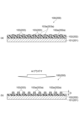
- FIG. 3 is a diagram showing a schematic diagram of a plasma process in the method of manufacturing the semiconductor device shown in FIG. 4A to 4C are diagrams showing a bonding method in the method of manufacturing the semiconductor device shown in FIG.
- the term “layer” includes structures with shapes formed over the entire surface when observed in a plan view, as well as structures with shapes formed on only a portion of the surface.
- the term “process” includes not only independent processes, but also processes that cannot be clearly distinguished from other processes, as long as the intended effect of the process is achieved.
- a numerical range indicated using “ ⁇ ” indicates a range that includes the numerical values before and after " ⁇ " as the minimum and maximum values, respectively.
- FIG. 1 is a cross-sectional view showing an example of a semiconductor device manufactured by the manufacturing method according to the present embodiment.
- the semiconductor device 1 is, for example, an example of a semiconductor package, and includes a plurality of semiconductor chips 10 and a semiconductor substrate 20, and has a chip-on-wafer (CoW) structure.
- the plurality of semiconductor chips 10 are manufactured by dicing a semiconductor substrate 100 described later into individual pieces.
- the plurality of semiconductor chips 10 are mounted on the semiconductor substrate 20 to form a three-dimensional mounting structure.
- the semiconductor substrate 20 may be a substrate on which a plurality of semiconductor chips, such as an LSI (Large scale Integrated Circuit) chip or a CMOS (Complementary Metal Oxide Semiconductor) sensor, are formed at locations corresponding to the respective semiconductor chips 10.
- Each semiconductor chip 10 may be a semiconductor chip such as an LSI or a memory.
- the plurality of semiconductor chips 10 and the semiconductor substrate 20 are finely bonded to each other by hybrid bonding described later, with the respective terminal electrodes and the insulating films around them being firmly and without misalignment. 1 , and a substrate portion that is a part of the semiconductor substrate 20 corresponding to the semiconductor chip 10.
- the manufacturing method according to the present embodiment may be applied to a W2W bonding process, in which case semiconductor substrates are bonded to each other.
- Figure 2 is a diagram sequentially showing a method for manufacturing the semiconductor device shown in Figure 1.
- Figure 3 is a diagram typically showing a plasma process in the method for manufacturing the semiconductor device shown in Figure 2.
- Figure 4 is a diagram showing a bonding method in the method for manufacturing the semiconductor device shown in Figure 2.
- the semiconductor device 1 can be manufactured, for example, through the following steps (a) to (j).
- a step of irradiating the insulating film 102 and the electrodes 103 of the semiconductor substrate 100 with plasma (e) A step of irradiating the insulating film 102 and the electrodes 103 of the semiconductor substrate 100 with plasma. (f) A step of irradiating the insulating film 202 and the electrodes 203 of the semiconductor substrate 200 with plasma. (g) A step of dividing the semiconductor substrate 100 into individual pieces to obtain a plurality of semiconductor chips 10, each of which has an insulating film portion 102b corresponding to the insulating film 102 and an electrode 103. (h) A step of aligning the electrodes 103 of each of the plurality of semiconductor chips 10 with the electrodes 203 of the semiconductor substrate 200 .
- Step (a) is a step of preparing a semiconductor substrate 100 (second semiconductor substrate) which is a silicon substrate on which integrated circuits made of semiconductor elements and wiring connecting them are formed, corresponding to a plurality of semiconductor chips 10.
- a semiconductor substrate 100 second semiconductor substrate
- step (a) is a step of preparing a semiconductor substrate 100 (second semiconductor substrate) which is a silicon substrate on which integrated circuits made of semiconductor elements and wiring connecting them are formed, corresponding to a plurality of semiconductor chips 10.
- step (a) as shown in FIG. 2A, a plurality of electrodes 103 (second electrodes) made of copper or aluminum are provided at predetermined intervals on one surface 101a of a substrate body 101 (second substrate body) made of silicon or the like, and an insulating film 102 (second organic insulating film) made of an inorganic material or an organic material is provided.
- the electrodes 103 are terminal electrodes for exposing the integrated circuits formed on the semiconductor substrate 100 to the outside through the insulating film 102.
- Step (b) is a step of preparing a semiconductor substrate 200 (first semiconductor substrate), which is a silicon substrate on which an integrated circuit consisting of semiconductor elements and wiring connecting them is formed.
- a plurality of electrodes 203 made of copper or aluminum or the like are provided at predetermined intervals on one surface 201a of a substrate body 201 (first substrate body) made of silicon or the like, and an insulating film 202 (first organic insulating film) made of an inorganic material or an organic material is provided.
- the electrodes 203 are terminal electrodes for exposing the integrated circuits formed on the semiconductor substrate 200 to the outside through the insulating film 202.
- the insulating film 202 may be provided on one surface 201a of the substrate body 201 before the plurality of electrodes 203 are provided, or the insulating film 202 may be provided on one surface 201a of the substrate body 201 before the plurality of electrodes 203 are provided.
- the insulating film 102 and the insulating film 202 used in the steps (a) and (b) are configured to include an organic material.
- the organic material used for the insulating film is, for example, polyimide, a polyimide precursor (for example, polyimide ester or polyamic acid), polyamideimide, benzocyclobutene (BCB), polybenzoxazole (PBO), or a PBO precursor. These organic materials have a lower elastic modulus than inorganic materials such as silicon oxide (SiO 2 ), and are soft materials.
- the elastic modulus of the organic material constituting the insulating film 102 and the insulating film 202 may be, for example, 7.0 GPa or less, 5.0 GPa or less, 3.5 GPa or less, 3.0 GPa or less, or 2.5 GPa or less.
- the elastic modulus here means Young's modulus.
- the organic material constituting the insulating film 102 and the insulating film 202 may preferably have a thermal expansion coefficient of 70 ppm/K or less, and more preferably 50 ppm/K or less.
- each insulating film can be easily formed as a thin film by spin coating or the like. Furthermore, since these organic materials have heat resistance, they can withstand the temperature (e.g., high temperature of 300° C. or more) when bonding the electrodes 103 and 203 in the step (j) described later, so that the bonding between the insulating films is not deteriorated by high temperature.
- photosensitive resin, thermosetting non-conductive film (NCF: Non Conductive Film), or thermosetting resin may be used as the organic material constituting the insulating film 102 and the insulating film 202. This organic material may be an underfill material.
- the insulating film 102 and the insulating film 202 may be insulating films containing both inorganic materials and organic materials, or one insulating film may be formed from an inorganic material and the other insulating film may be formed from an organic material.
- the inorganic material used for the insulating film is, for example, silicon oxide (SiO 2 ).
- the thickness of the insulating film 102 may be 20 ⁇ m or less. By making the thickness of the insulating film 102 sufficiently thin, the wiring formed from the electrode 103 can be made finer.
- the minimum size (electrode width) of the electrode 103 formed in the insulating film 102 is determined by the thickness of the insulating film 102 and the aspect ratio of the photosensitive material used. When the aspect ratio of the photosensitive material is, for example, 1:1 (opening width: depth), the electrode width of the electrode 103 can be made 20 ⁇ m or less by making the thickness of the insulating film 102 20 ⁇ m or less.
- the thickness of the insulating film 102 may be thicker than 20 ⁇ m.
- step (i) described later when the insulating films are bonded together in step (i) described later, more foreign matter can be embedded in the resin insulating film 102, and the insulating films can be bonded together more reliably.
- the thickness of the insulating film 102 may be 4 ⁇ m or more.
- the size of foreign objects that can be embedded in the insulating film 102 is determined by the thickness of the resin insulating film 102. If the thickness of the insulating film 102 is, for example, 4 ⁇ m, a foreign object with a diameter or width of 4 ⁇ m can be embedded in the insulating film 102.
- the thickness of the insulating film 202 may be 20 ⁇ m or less, or may be thicker than 20 ⁇ m, or may be 4 ⁇ m or more, like the insulating film 102. As described above, the insulating film 202 may embed the debris.
- Step (c) is a step of polishing the semiconductor substrate 100.
- step (c) the surface of the insulating film 102 on which the electrode 103 is provided is polished by using a CMP (Chemical Mechanical Polishing) method. This is because the surface of the insulating film 102 may become rough due to the plasma irradiation in the step (e), and the surface may become rough when the insulating film 102 is bonded by hybrid bonding. This is to reduce the average roughness of the surface of the insulating film 102 beforehand, before the insulating film 102 is polished.
- CMP Chemical Mechanical Polishing
- the average roughness of the surface of the insulating film 102 is reduced to 5 nm or less, preferably 1 nm or less, and This polishing may remove debris on the surface of the semiconductor substrate 100.
- the surface 102a of the insulating film 102 and the tip surface 103a of the electrode 103 may be polished. It may form a part of the step.
- Step (d) is a step of polishing the semiconductor substrate 200.
- step (d) the surface of the insulating film 202 on which the electrode 203 is provided is polished using a CMP method. This polishing is preferably performed before step (f). This is because, as in step (c), the surface of the insulating film 202 may become rough due to the plasma irradiation in step (f), and the average roughness of the surface of the insulating film 202 is reduced before bonding by hybrid bonding. By such polishing, the average roughness of the surface of the insulating film 202 is reduced to 5 nm or less, preferably 1 nm or less, making it possible to perform hybrid bonding, which will be described later. By this polishing, debris on the surface of the semiconductor substrate 200 may be removed. Note that, in this polishing step, part of the step between the surface 202a of the insulating film 202 and the tip surface 203a of the electrode 203 may be formed.
- the insulating film 102 and the insulating film 202 may be polished to have the same thickness, or, for example, the insulating film 102 may be polished to have a thickness greater than that of the insulating film 202. On the other hand, the insulating film 102 may be polished to have a thickness less than that of the insulating film 202.
- the insulating film 102 is thicker than the insulating film 202 and is made of an organic material, the insulating film 102 can contain most of the debris that adheres to the bonding interface during dicing into semiconductor chips 10 or during chip mounting, thereby reducing bonding defects.
- the insulating film 102 is thinner than the insulating film 202, the height of the mounted semiconductor chip 10, i.e., the semiconductor device 1, can be reduced.
- Step (e) is a step of irradiating plasma to the insulating film 102 and the electrode 103 of the semiconductor substrate 100.
- the insulating film 102 is etched by the plasma so that the surface 102a of the insulating film 102 is closer to the substrate body 101 (toward the back side) than the tip surface 103a of the electrode 103.
- the plasma used in step (e) is, for example, argon (Ar) plasma, and the semiconductor substrate 100 is placed in a reduced pressure chamber, and the surface of the semiconductor substrate 100 is irradiated with argon plasma to perform etching.
- the conditions of the argon plasma may be such that the flow rate of the plasma gas (argon gas) is 3.38 ⁇ 10 ⁇ 2 Pa ⁇ m 3 /sec (20 sccm) to 1.69 Pa ⁇ m 3 /sec (1000 sccm) (all of which refer to flow rates at 1 atmosphere and 0° C.), the plasma output may be 10 W to 1000 W, and the plasma processing time may be 30 seconds or more. The plasma processing time may be 500 seconds or less.
- the step D between the surface 102a of the insulating film 102 and the tip surface 103a of the electrode 103 becomes 40 nm or more and 100 nm or less.
- Such a step D is formed due to the difference in elastic modulus between the insulating film 102 and the electrode 103.
- Plasma may be irradiated so that the step D between the surface 102a of the insulating film 102 and the tip surface 103a of the electrode 103 becomes 60 nm or more and 80 nm or less.
- the plasma to be used is preferably argon plasma, but is not limited to this, and oxygen plasma or the like may also be used.
- Step (f) is a step of irradiating plasma to the insulating film 202 and the electrode 203 of the semiconductor substrate 200.
- the insulating film 202 is etched by the plasma so that the surface 202a of the insulating film 202 is closer to the substrate body 201 (toward the back side) than the tip surface 203a of the electrode 203.
- the plasma used in step (f) is, for example, argon (Ar) plasma, and the semiconductor substrate 200 is placed in a reduced pressure chamber, and the surface of the semiconductor substrate 200 is irradiated with argon plasma to perform etching.
- the conditions of the argon plasma may be such that the flow rate of the plasma gas (argon gas) is 3.38 ⁇ 10 ⁇ 2 Pa ⁇ m 3 /sec (20 sccm) to 1.69 Pa ⁇ m 3 /sec (1000 sccm) (all of which refer to flow rates at 1 atmosphere and 0° C.), the plasma output may be 10 W to 1000 W, and the plasma processing time may be 30 seconds or more. The plasma processing time may be 500 seconds or less.
- the step D between the surface 202b of the insulating film 202 and the tip surface 203a of the electrode 203 becomes 40 nm or more and 100 nm or less.
- Such a step D is formed due to the difference in elastic modulus between the insulating film 202 and the electrode 203.
- Plasma may be irradiated so that the step D between the surface 202b of the insulating film 202 and the tip surface 203a of the electrode 203 becomes 60 nm or more and 80 nm or less.
- a plasma other than argon may be used.
- Step (g) is a step of dividing the semiconductor substrate 100 into individual pieces to obtain a plurality of semiconductor chips 10.
- the polished semiconductor substrate 100 is divided into individual pieces to obtain a plurality of semiconductor chips 10 (semiconductor substrates), each of which has an insulating film portion 102b corresponding to the insulating film 102 and at least one electrode 103.
- the semiconductor substrate 100 is placed on a dicing tape, and divided into a plurality of semiconductor chips 10 by a cutting means such as dicing from the insulating film 102 toward the substrate body 101.
- the insulating film 102 When dicing the semiconductor substrate 100, the insulating film 102 may be covered with a protective material or the like, and then divided into individual pieces.
- the insulating film 102 of the semiconductor substrate 100 is divided into insulating film portions 102b corresponding to each semiconductor chip 10, as shown in (b) of FIG. 2.
- the substrate body 101 is divided into corresponding substrate portions 101b.
- a dicing method for dividing the semiconductor substrate 100 for example, plasma dicing, stealth dicing, or laser dicing can be used. After the division by dicing is completed in step (g), the divided semiconductor chips 10 may be washed.
- Step (h) is a step of aligning the electrodes 103 of each of the semiconductor chips 10 with respect to the electrodes 203 of the semiconductor substrate 200, as shown in FIG. 2(c) (left side) and FIG. 4(a).
- the semiconductor chips 10 are aligned so that the electrodes 103 of each semiconductor chip 10 face the corresponding electrodes 203 of the semiconductor substrate 200.
- FIG. 4(a) is a schematic diagram showing an enlarged portion of FIG. 2(c).
- a step is formed between the insulating film portion 102b and the electrode 103, and between the insulating film 202 and the electrode 203. That is, the electrodes 103 and 203 are in a state of protruding from the surfaces of the insulating film portion 102b and the insulating film 202.
- Step (i) is a step of bonding each insulating film portion 102b of the multiple semiconductor chips 10 to the insulating film 202 of the semiconductor substrate 200.
- step (i) after removing organic matter or metal oxide attached to the surface of each semiconductor chip 10 and the semiconductor substrate 200, the semiconductor chip 10 is aligned with the semiconductor substrate 200.
- the insulating film portion 102b of each of the multiple semiconductor chips 10 is bonded to the insulating film 202 of the semiconductor substrate 200 as hybrid bonding.
- the insulating film portions 102b of the multiple semiconductor chips 10 and the insulating film 202 of the semiconductor substrate 200 may be uniformly heated before bonding.
- the insulating film made of an organic material expands more than the electrode, and the step between the insulating film portion 102b and the electrode 103 and the step between the insulating film 202 and the electrode 203 are eliminated.
- the step may be completely eliminated, the surfaces of the insulating film portion 102b and the electrode 103 may be flush, and the surfaces of the insulating film 202 and the electrode 203 may be flush, or a slight step may remain.
- the temperature difference between the semiconductor chip 10 and the semiconductor substrate 200 during bonding is preferably, for example, 10° C. or less.
- the insulating film portion 102b and the insulating film 202 are bonded to each other to form an insulating bonded portion, and the multiple semiconductor chips 10 are mechanically and firmly attached to the semiconductor substrate 200.
- the heat bonding is performed at a uniform temperature, positional deviations at the bonding points are unlikely to occur, and high-precision bonding can be performed.
- the electrodes 103 of the semiconductor chip 10 and the electrodes 203 of the semiconductor substrate 200 are separated from each other and are not connected (but are aligned).
- the semiconductor chip 10 may be bonded to the semiconductor substrate 200 by other bonding methods, for example, room temperature bonding.
- Step (j) is a step of bonding the electrodes 103 of each of the semiconductor chips 10 to the electrodes 203 of the semiconductor substrate 200.
- step (j) as shown in FIG. 2(d), when the bonding in step (i) is completed, a predetermined heat H or pressure or both are applied to bond the electrodes 103 of the semiconductor chips 10 to the electrodes 203 of the semiconductor substrate 200 as hybrid bonding.
- the annealing temperature in step (j) is preferably 150° C. or higher and 400° C. or lower, and more preferably 200° C. or higher and 300° C. or lower.
- the electrode 103 and the corresponding electrode 203 are bonded to form an electrode bonding portion, and the electrodes 103 and 203 are mechanically and electrically bonded firmly.
- the electrode bonding in step (j) is performed after the bonding in step (i), but may be performed simultaneously with the bonding in step (i). Thereafter, all the semiconductor chips 10 are bonded to the semiconductor substrate 200 to obtain the semiconductor device 1 shown in FIG.
- a semiconductor device 1 can be obtained in which multiple semiconductor chips 10 are electrically and mechanically installed at predetermined positions with high precision on the semiconductor substrate 200.
- the semiconductor device (CoW) having the configuration shown in FIG. 1 may be further diced to form individual semiconductor devices each composed of one semiconductor chip 10 and a portion of the semiconductor substrate 200 corresponding to that one semiconductor chip 10.
- the insulating films 102, 202 are etched by plasma so that the surfaces of the insulating films 102, 202 are closer to the substrate body 101, 201 than the tip surfaces of the electrodes 103, 203.
- plasma is irradiated toward both the insulating films 102, 202 and the electrodes 103, 203, the amount of etching by the plasma differs depending on the difference in elastic modulus between the two.
- this manufacturing method by changing the plasma conditions depending on the materials of the organic insulating film and the electrodes or the difference in elastic modulus between the two, in the hybrid bonding method using the insulating films 102, 202, it is possible to easily provide a desired step D between the surface of the insulating film 202 of the semiconductor substrate 100, 200 and the tip surfaces of the electrodes 103, 203.
- the method for manufacturing a semiconductor device it is preferable to irradiate the semiconductor substrates 100 and 200 with argon plasma in steps (e) and (f). In this case, it becomes easier to adjust the step between the surface of the insulating film 102 or 202 of the semiconductor substrate 100 or 200 and the tip surface of the electrode 103 or 203 to a desired value.
- the flow rate of the plasma gas in steps (e) and (f) is preferably 3.38 ⁇ 10 ⁇ 2 Pa ⁇ m 3 /sec (20 sccm) to 1.69 Pa ⁇ m 3 /sec (1000 sccm).
- the flow rate of the plasma gas is 3.38 ⁇ 10 ⁇ 2 Pa ⁇ m 3 /sec (20 sccm) or more, etching by plasma can be promoted, and the step between the surface of the insulating film 102, 202 of the semiconductor substrate 100, 200 and the tip surface of the electrode 103, 203 can be set to a desired value early.
- the plasma output in steps (e) and (f) is preferably 10 W to 1000 W.
- the plasma output is preferably 10 W to 1000 W.
- etching by the plasma can be promoted, and the step between the surface of the insulating film 102, 202 of the semiconductor substrate 100, 200 and the tip surface of the electrode 103, 203 can be quickly set to the desired value.
- the plasma output is set to 1000 W or less, roughening of the surfaces of the insulating film 102, 202 and the electrode 103, 203 by the plasma can be suppressed.
- the plasma treatment time in steps (e) and (f) is preferably 30 seconds or more.
- the plasma treatment time is preferably 30 seconds or more.
- the elastic modulus of the insulating films 102, 202 is preferably 7.5 GPa or less. In this case, it is possible to easily provide a desired step between the surface of the insulating films 102, 202 of the semiconductor substrates 100, 200 and the tip surfaces of the electrodes 103, 203.
- plasma may be irradiated onto the surfaces of the semiconductor substrates 100 and 200 so that the step distance between the surfaces of the insulating films 102 and 202 and the tip surfaces of the electrodes 103 and 203 is 40 nm or more and 100 nm or less.
- the amount of misalignment between the surfaces of the insulating films 102 and 202 and the tip surfaces of the electrodes 103 and 203 is reduced due to thermal expansion, making it possible to more reliably bond the semiconductor substrates 100 and 200 to each other.
- plasma may be irradiated onto the surfaces of the semiconductor substrates 100 and 200 so that the step distance between the surfaces of the insulating films 102 and 202 and the tip surfaces of the electrodes 103 and 203 is 60 nm or more and 80 nm or less.
- the amount of misalignment between the surfaces of the insulating films 102 and 202 and the tip surfaces of the electrodes 103 and 203 is reduced due to thermal expansion, making it possible to more reliably bond the semiconductor substrates 100 and 200 to each other.
- the manufacturing method of the semiconductor device further includes a step of polishing the insulating film 102, 202 and the electrode 103, 203 provided on one side of the semiconductor substrate 100, 200, and the step of polishing the semiconductor substrate 100, 200 is preferably performed before the steps (e) and (f) of irradiating with plasma.
- the step between the surface of the insulating film 102, 202 of the semiconductor substrate 100, 200 and the tip surface of the electrode 103, 203 can be set to a desired value by irradiating with plasma, depending on the output state of the plasma, the surface roughness of the surface of the insulating film 102, 202 or the tip surface of the electrode 103, 203 may be deteriorated.
- the polishing steps (c) and (d) it is preferable to polish the surfaces of the insulating films 102, 202 and the electrodes 103, 203 so that their surface roughness Ra is 5 nm or less, preferably 1 nm or less. In this case, it is possible to more reliably reduce bonding defects in hybrid bonding.
- the resin material contained in the insulating films 102, 202 may include bismaleimide, polyimide, polyimide precursor, polyamideimide, benzocyclobutene (BCB), polybenzoxazole (PBO), or PBO precursor. These materials are liquid or soluble in a solvent, making it easy to prepare the insulating films 102, 202, for example, by spin coating, and to form thin films. In addition, these materials have high heat resistance, so they can withstand the high temperatures that are generated when the semiconductor chip 10 (semiconductor substrate 100) is bonded to the semiconductor substrate 200, making it possible to bond the substrates more reliably.
- the present disclosure is not limited to the above embodiments and can be applied to various embodiments.
- the above describes a method for manufacturing a semiconductor device using a CoW bonding process as an example of hybrid bonding, but the method for manufacturing a semiconductor device according to this embodiment may also be applied to a Wafer-to-Wafer (W2W) bonding process.
- W2W Wafer-to-Wafer
- the semiconductor substrate 100 and semiconductor substrate 200 that have been subjected to steps (e) and (f) are bonded by hybrid bonding without performing step (g) of dividing the first semiconductor substrate into individual pieces by dicing.
- a semiconductor substrate was prepared with an organic insulating film and an electrode on one surface of the substrate body, and plasma was irradiated onto the semiconductor substrate to test whether the step between the surface of the organic insulating film and the tip surface of the electrode could be adjusted.
- a test wafer corresponding to the semiconductor substrate 100 was prepared.
- a first polyimide material and a second polyimide material were prepared as materials for an organic insulating film used in the test wafer.
- the first polyimide material had a glass transition temperature of 290° C. after curing, a linear expansion coefficient (CTE) of 100 ppm/° C. (10 ⁇ 6 /° C.), and an elastic modulus of 2.5 GPa.
- the second polyimide material had a glass transition temperature of 267° C. after curing, a linear expansion coefficient (CTE) of 75 ppm/° C., and an elastic modulus of 3.1 GPa.
- the linear expansion coefficient of copper used for the electrodes was 16.8 ppm/° C. (10 ⁇ 6 /° C.), and an elastic modulus of 120 GPa.
- Electrodes 103 which are copper pillars (Cu) of 10 ⁇ m square and 6 ⁇ m high, were fabricated by a semi-additive method on a substrate body 101, which is a silicon substrate.
- the above-mentioned first polyimide material was spin-coated on the substrate body 101 to cover the electrodes 103, and baked at 375°C for 2 hours in a nitrogen atmosphere to harden (see Fig. 3(a)).
- the hardened semiconductor substrate 100 was placed in a reduced pressure chamber, and argon plasma was irradiated to the semiconductor substrate 100 under the following plasma conditions (see Fig. 3(b)).
- RF output plasma output
- Treatment time (plasma treatment time): 120 seconds
- Step D between the surface of the organic insulating film and the tip face of the electrode, the surface roughness Ra of the surface of the organic insulating film, and the surface roughness Ra of the tip face of the electrode were measured, and the following results were obtained.
- the step D was in the range of 40 nm to 80 nm, which is the range in which the compression bonding property of the hybrid bonding is good (when the elastic modulus is 2.5 GPa). It was also confirmed that the surface roughness Ra of the organic insulating film and the electrode was also suppressed to a low value.
- Experimental Examples 11 to 17 were performed.
- a first polyimide material having an elastic modulus of 2.5 GPa was used as in Experimental Example 1, and the plasma conditions were changed to irradiate the semiconductor substrate 100 with plasma.
- Conditions other than the plasma irradiation conditions were the same as in Experimental Example 1.
- the plasma conditions and test results in Experimental Examples 11 to 17 were as shown in Table 3 below.
- tests were performed with plasma conditions that were significantly changed compared to Experimental Example 1 and the like.
- 1...semiconductor device 10...semiconductor chip, 20...semiconductor substrate, 100, 200...semiconductor substrate, 101, 201...substrate body, 101a, 201a...one surface, 102, 202...insulating film, 102a, 202a...surface, 102b...insulating film portion, 103, 203...electrode, 103a, 203a...tip surface, D...step.
Landscapes
- Internal Circuitry In Semiconductor Integrated Circuit Devices (AREA)
- Formation Of Insulating Films (AREA)
- Engineering & Computer Science (AREA)
- Manufacturing & Machinery (AREA)
Priority Applications (6)
| Application Number | Priority Date | Filing Date | Title |
|---|---|---|---|
| PCT/JP2023/014899 WO2024214219A1 (ja) | 2023-04-12 | 2023-04-12 | 半導体装置の製造方法 |
| KR1020257035541A KR20250173514A (ko) | 2023-04-12 | 2023-04-12 | 반도체 장치의 제조 방법 |
| US18/857,188 US20260082837A1 (en) | 2023-04-12 | 2023-04-12 | Method for manufacturing semiconductor device |
| JP2025513575A JPWO2024214219A1 (https=) | 2023-04-12 | 2023-04-12 | |
| CN202380035614.0A CN119137712A (zh) | 2023-04-12 | 2023-04-12 | 半导体装置的制造方法 |
| TW113113324A TW202510081A (zh) | 2023-04-12 | 2024-04-10 | 半導體裝置之製造方法 |
Applications Claiming Priority (1)
| Application Number | Priority Date | Filing Date | Title |
|---|---|---|---|
| PCT/JP2023/014899 WO2024214219A1 (ja) | 2023-04-12 | 2023-04-12 | 半導体装置の製造方法 |
Publications (1)
| Publication Number | Publication Date |
|---|---|
| WO2024214219A1 true WO2024214219A1 (ja) | 2024-10-17 |
Family
ID=93058878
Family Applications (1)
| Application Number | Title | Priority Date | Filing Date |
|---|---|---|---|
| PCT/JP2023/014899 Ceased WO2024214219A1 (ja) | 2023-04-12 | 2023-04-12 | 半導体装置の製造方法 |
Country Status (6)
| Country | Link |
|---|---|
| US (1) | US20260082837A1 (https=) |
| JP (1) | JPWO2024214219A1 (https=) |
| KR (1) | KR20250173514A (https=) |
| CN (1) | CN119137712A (https=) |
| TW (1) | TW202510081A (https=) |
| WO (1) | WO2024214219A1 (https=) |
Citations (9)
| Publication number | Priority date | Publication date | Assignee | Title |
|---|---|---|---|---|
| JP2000340549A (ja) * | 1999-06-01 | 2000-12-08 | Canon Inc | エッチング方法及びそれを用いた半導体装置の製造方法 |
| JP2004038047A (ja) * | 2002-07-05 | 2004-02-05 | Alps Electric Co Ltd | アクティブマトリクス基板及びその製造方法並びにそれを用いた表示装置 |
| JP2006085916A (ja) * | 2004-09-14 | 2006-03-30 | Kyodo Printing Co Ltd | 有機elディスプレイ及びその製造方法 |
| JP2006106575A (ja) * | 2004-10-08 | 2006-04-20 | Mitsubishi Electric Corp | アクティブマトリクス型表示装置およびアクティブマトリクス型表示装置の製造方法 |
| JP2009015199A (ja) * | 2007-07-09 | 2009-01-22 | Nec Lcd Technologies Ltd | 液晶表示装置およびその製造方法 |
| JP2010230978A (ja) * | 2009-03-27 | 2010-10-14 | Fujitsu Ltd | 光半導体装置及びその製造方法 |
| JP2021197430A (ja) * | 2020-06-12 | 2021-12-27 | 昭和電工マテリアルズ株式会社 | 半導体装置の製造方法 |
| WO2022203020A1 (ja) * | 2021-03-26 | 2022-09-29 | 昭和電工マテリアルズ株式会社 | 半導体装置の製造方法、半導体装置、集積回路要素、及び、集積回路要素の製造方法 |
| WO2022203027A1 (ja) * | 2021-03-26 | 2022-09-29 | 昭和電工マテリアルズ株式会社 | 半導体装置の製造方法、洗浄装置、洗浄方法、及び、半導体装置 |
Family Cites Families (2)
| Publication number | Priority date | Publication date | Assignee | Title |
|---|---|---|---|---|
| US9953941B2 (en) | 2015-08-25 | 2018-04-24 | Invensas Bonding Technologies, Inc. | Conductive barrier direct hybrid bonding |
| JP7501133B2 (ja) | 2020-06-12 | 2024-06-18 | 株式会社レゾナック | 半導体装置の製造方法 |
-
2023
- 2023-04-12 JP JP2025513575A patent/JPWO2024214219A1/ja active Pending
- 2023-04-12 CN CN202380035614.0A patent/CN119137712A/zh active Pending
- 2023-04-12 KR KR1020257035541A patent/KR20250173514A/ko active Pending
- 2023-04-12 WO PCT/JP2023/014899 patent/WO2024214219A1/ja not_active Ceased
- 2023-04-12 US US18/857,188 patent/US20260082837A1/en active Pending
-
2024
- 2024-04-10 TW TW113113324A patent/TW202510081A/zh unknown
Patent Citations (9)
| Publication number | Priority date | Publication date | Assignee | Title |
|---|---|---|---|---|
| JP2000340549A (ja) * | 1999-06-01 | 2000-12-08 | Canon Inc | エッチング方法及びそれを用いた半導体装置の製造方法 |
| JP2004038047A (ja) * | 2002-07-05 | 2004-02-05 | Alps Electric Co Ltd | アクティブマトリクス基板及びその製造方法並びにそれを用いた表示装置 |
| JP2006085916A (ja) * | 2004-09-14 | 2006-03-30 | Kyodo Printing Co Ltd | 有機elディスプレイ及びその製造方法 |
| JP2006106575A (ja) * | 2004-10-08 | 2006-04-20 | Mitsubishi Electric Corp | アクティブマトリクス型表示装置およびアクティブマトリクス型表示装置の製造方法 |
| JP2009015199A (ja) * | 2007-07-09 | 2009-01-22 | Nec Lcd Technologies Ltd | 液晶表示装置およびその製造方法 |
| JP2010230978A (ja) * | 2009-03-27 | 2010-10-14 | Fujitsu Ltd | 光半導体装置及びその製造方法 |
| JP2021197430A (ja) * | 2020-06-12 | 2021-12-27 | 昭和電工マテリアルズ株式会社 | 半導体装置の製造方法 |
| WO2022203020A1 (ja) * | 2021-03-26 | 2022-09-29 | 昭和電工マテリアルズ株式会社 | 半導体装置の製造方法、半導体装置、集積回路要素、及び、集積回路要素の製造方法 |
| WO2022203027A1 (ja) * | 2021-03-26 | 2022-09-29 | 昭和電工マテリアルズ株式会社 | 半導体装置の製造方法、洗浄装置、洗浄方法、及び、半導体装置 |
Also Published As
| Publication number | Publication date |
|---|---|
| KR20250173514A (ko) | 2025-12-10 |
| CN119137712A (zh) | 2024-12-13 |
| TW202510081A (zh) | 2025-03-01 |
| JPWO2024214219A1 (https=) | 2024-10-17 |
| US20260082837A1 (en) | 2026-03-19 |
Similar Documents
| Publication | Publication Date | Title |
|---|---|---|
| JP7543712B2 (ja) | 半導体装置の製造方法 | |
| US12557615B2 (en) | Methods for bonding semiconductor elements | |
| EP3537472B1 (en) | Method for transferring device layer to transfer substrate | |
| US20070273018A1 (en) | Semiconductor apparatus and method for manufacturing the same | |
| JP2004335641A (ja) | 半導体素子内蔵基板の製造方法 | |
| JP7501133B2 (ja) | 半導体装置の製造方法 | |
| TW201442168A (zh) | 中介層用基板及其製造方法 | |
| US8642390B2 (en) | Tape residue-free bump area after wafer back grinding | |
| Wang et al. | Fabrication and characterization of flexible ultrathin chip package using photosensitive polyimide | |
| US20250336881A1 (en) | Method for manufacturing semiconductor device | |
| JP3920195B2 (ja) | 電子部品実装構造及びその製造方法 | |
| JP2023173119A (ja) | 半導体装置の製造方法 | |
| Kayaba et al. | A new adhesive for CoW Cu-Cu hybrid bonding with high throughput and room temperature pre-bonding | |
| US20240170447A1 (en) | Semiconductor device manufacturing method, semiconductor device, integrated circuit element, and integrated circuit element manufacturing method | |
| US20030171001A1 (en) | Method of manufacturing semiconductor devices | |
| WO2024214219A1 (ja) | 半導体装置の製造方法 | |
| TW200933844A (en) | Wafer level package with die receiving through-hole and method of the same | |
| WO2026078823A1 (ja) | 半導体装置の製造方法 | |
| WO2026078856A1 (ja) | 半導体装置の製造方法 | |
| Rao et al. | Development of mold-first fan-out panel-level packaging (fo-plp) on 600mm x 600mm size panel | |
| TWI425580B (zh) | 製造半導體晶片封裝模組之方法 | |
| WO2024189923A1 (ja) | 半導体装置の製造方法、及び、ダイシングテープ | |
| US20260123496A1 (en) | Substrate and manufacturing method for the same | |
| WO2025104788A1 (ja) | 半導体装置の製造方法、及び半導体装置 | |
| WO2026069655A1 (ja) | 半導体装置および半導体装置の製造方法 |
Legal Events
| Date | Code | Title | Description |
|---|---|---|---|
| WWE | Wipo information: entry into national phase |
Ref document number: 202380035614.0 Country of ref document: CN |
|
| 121 | Ep: the epo has been informed by wipo that ep was designated in this application |
Ref document number: 23932995 Country of ref document: EP Kind code of ref document: A1 |
|
| ENP | Entry into the national phase |
Ref document number: 2025513575 Country of ref document: JP Kind code of ref document: A |
|
| WWE | Wipo information: entry into national phase |
Ref document number: 2025513575 Country of ref document: JP |
|
| ENP | Entry into the national phase |
Ref document number: 1020257035541 Country of ref document: KR Free format text: ST27 STATUS EVENT CODE: A-0-1-A10-A15-NAP-PA0105 (AS PROVIDED BY THE NATIONAL OFFICE) |
|
| WWE | Wipo information: entry into national phase |
Ref document number: KR1020257035541 Country of ref document: KR |
|
| NENP | Non-entry into the national phase |
Ref country code: DE |
|
| 122 | Ep: pct application non-entry in european phase |
Ref document number: 23932995 Country of ref document: EP Kind code of ref document: A1 |