WO2024203872A1 - 高周波電力増幅装置 - Google Patents
高周波電力増幅装置 Download PDFInfo
- Publication number
- WO2024203872A1 WO2024203872A1 PCT/JP2024/011341 JP2024011341W WO2024203872A1 WO 2024203872 A1 WO2024203872 A1 WO 2024203872A1 JP 2024011341 W JP2024011341 W JP 2024011341W WO 2024203872 A1 WO2024203872 A1 WO 2024203872A1
- Authority
- WO
- WIPO (PCT)
- Prior art keywords
- power amplifier
- frequency power
- high frequency
- input
- shunt circuit
- Prior art date
- Legal status (The legal status is an assumption and is not a legal conclusion. Google has not performed a legal analysis and makes no representation as to the accuracy of the status listed.)
- Ceased
Links
Images








Classifications
-
- H—ELECTRICITY
- H03—ELECTRONIC CIRCUITRY
- H03F—AMPLIFIERS
- H03F1/00—Details of amplifiers with only discharge tubes, only semiconductor devices or only unspecified devices as amplifying elements
- H03F1/56—Modifications of input or output impedances, not otherwise provided for
- H03F1/565—Modifications of input or output impedances, not otherwise provided for using inductive elements
-
- H—ELECTRICITY
- H03—ELECTRONIC CIRCUITRY
- H03F—AMPLIFIERS
- H03F3/00—Amplifiers with only discharge tubes or only semiconductor devices as amplifying elements
- H03F3/189—High-frequency amplifiers, e.g. radio frequency amplifiers
- H03F3/19—High-frequency amplifiers, e.g. radio frequency amplifiers with semiconductor devices only
-
- H—ELECTRICITY
- H03—ELECTRONIC CIRCUITRY
- H03F—AMPLIFIERS
- H03F1/00—Details of amplifiers with only discharge tubes, only semiconductor devices or only unspecified devices as amplifying elements
- H03F1/32—Modifications of amplifiers to reduce non-linear distortion
-
- H—ELECTRICITY
- H03—ELECTRONIC CIRCUITRY
- H03F—AMPLIFIERS
- H03F1/00—Details of amplifiers with only discharge tubes, only semiconductor devices or only unspecified devices as amplifying elements
- H03F1/32—Modifications of amplifiers to reduce non-linear distortion
- H03F1/3205—Modifications of amplifiers to reduce non-linear distortion in field-effect transistor amplifiers
-
- H—ELECTRICITY
- H03—ELECTRONIC CIRCUITRY
- H03F—AMPLIFIERS
- H03F1/00—Details of amplifiers with only discharge tubes, only semiconductor devices or only unspecified devices as amplifying elements
- H03F1/42—Modifications of amplifiers to extend the bandwidth
-
- H—ELECTRICITY
- H03—ELECTRONIC CIRCUITRY
- H03F—AMPLIFIERS
- H03F3/00—Amplifiers with only discharge tubes or only semiconductor devices as amplifying elements
- H03F3/189—High-frequency amplifiers, e.g. radio frequency amplifiers
- H03F3/19—High-frequency amplifiers, e.g. radio frequency amplifiers with semiconductor devices only
- H03F3/193—High-frequency amplifiers, e.g. radio frequency amplifiers with semiconductor devices only with field-effect devices
-
- H—ELECTRICITY
- H03—ELECTRONIC CIRCUITRY
- H03F—AMPLIFIERS
- H03F3/00—Amplifiers with only discharge tubes or only semiconductor devices as amplifying elements
- H03F3/189—High-frequency amplifiers, e.g. radio frequency amplifiers
- H03F3/19—High-frequency amplifiers, e.g. radio frequency amplifiers with semiconductor devices only
- H03F3/195—High-frequency amplifiers, e.g. radio frequency amplifiers with semiconductor devices only in integrated circuits
-
- H—ELECTRICITY
- H03—ELECTRONIC CIRCUITRY
- H03F—AMPLIFIERS
- H03F3/00—Amplifiers with only discharge tubes or only semiconductor devices as amplifying elements
- H03F3/60—Amplifiers in which coupling networks have distributed constants, e.g. with waveguide resonators
- H03F3/601—Amplifiers in which coupling networks have distributed constants, e.g. with waveguide resonators using FET's, e.g. GaAs FET's
-
- H—ELECTRICITY
- H03—ELECTRONIC CIRCUITRY
- H03F—AMPLIFIERS
- H03F2200/00—Indexing scheme relating to amplifiers
- H03F2200/246—A series resonance being added in shunt in the input circuit, e.g. base, gate, of an amplifier stage, e.g. as a trap
-
- H—ELECTRICITY
- H03—ELECTRONIC CIRCUITRY
- H03F—AMPLIFIERS
- H03F2200/00—Indexing scheme relating to amplifiers
- H03F2200/402—A series resonance being added in shunt in the output circuit, e.g. base, gate, of an amplifier stage
-
- H—ELECTRICITY
- H03—ELECTRONIC CIRCUITRY
- H03F—AMPLIFIERS
- H03F2200/00—Indexing scheme relating to amplifiers
- H03F2200/451—Indexing scheme relating to amplifiers the amplifier being a radio frequency amplifier
Definitions
- This disclosure relates to a high-frequency power amplifier device used in a device that transmits high-frequency signals.
- n78 which is specified for 5G NR in 3GPP (registered trademark), has a bandwidth of 500 MHz from 3.3 GHz to 3.8 GHz, and there is a demand for this to be covered by a single high frequency power amplifier.
- GaN gallium nitride
- Patent Document 1 discloses a radio frequency power amplifier in which a plurality of unit transistors are arranged on a semiconductor substrate, and a series resonant circuit is shunt-connected to the control terminal of each unit transistor.
- Patent Document 2 also discloses a high-frequency semiconductor device in the form of a microwave monolithic integrated circuit (MMIC) in which multiple unit transistors connected in parallel and series resonant circuits shunt-connected to the control terminals of each unit transistor are integrated on a single semiconductor substrate.
- MMIC microwave monolithic integrated circuit
- the configuration of Patent Document 2 has a smaller inductor component because the control terminal and the series resonant circuit, and the series resonant circuit and the via hole are directly connected by wiring on the semiconductor substrate, and the higher the frequency, the less the effect of characteristic degradation is, making it more effective.
- the risk of characteristic fluctuations due to variations in wire length during assembly can be reduced.
- Patent Document 2 also assumes that there is only one wire from the gate connection wiring to the control terminal of the unit transistor, which has the same issues as Patent Document 1.
- the present disclosure therefore aims to provide a high-frequency power amplifier device that can reduce the effects of wire length variations and suppress variations in high-frequency characteristics, including gain, within a semiconductor substrate and between high-frequency power amplifier devices.
- a radio frequency power amplifier includes a submount substrate having a wiring pattern, a semiconductor substrate mounted on the submount substrate, a plurality of unit amplifiers mounted on the semiconductor substrate, and a plurality of input wires for transmitting RF signals input to the plurality of unit amplifiers, each of the plurality of unit amplifiers having a radio frequency transistor having a plurality of gate fingers, a gate bus line connecting the plurality of gate fingers of the radio frequency transistor, an input bonding pad connected to the gate bus line, and a shunt circuit having one end connected to the input bonding pad and the other end connected to a ground potential, the plurality of input wires include a plurality of input wires connecting the wiring pattern and the input bonding pad of the unit amplifier for each of the plurality of unit amplifiers, the gate bus lines of each of the plurality of unit amplifiers are all physically spaced apart from each other, and the shunt circuit of each of the plurality of unit amplifiers includes a semiconductor inductor and
- the high frequency power amplifier device disclosed herein can reduce variations in high frequency characteristics, including gain, within a semiconductor substrate and between high frequency power amplifier devices.
- FIG. 1A is a diagram showing an example of a plan view of a high frequency power amplifier device according to a first embodiment.
- FIG. 1B is a diagram showing an example of an equivalent circuit diagram of the high frequency power amplifier device according to the first embodiment.
- FIG. 2A is a diagram illustrating an example of a plan view of a high frequency power amplifier device according to a second embodiment.
- FIG. 2B is a diagram showing an example of an equivalent circuit diagram of the high frequency power amplifier device according to the second embodiment.
- FIG. 3A is a diagram illustrating an example of a plan view of a high frequency power amplifier device according to a third embodiment.
- FIG. 3B is a diagram showing an example of an equivalent circuit diagram of the high frequency power amplifier device according to the third embodiment.
- FIG. 1A is a diagram showing an example of a plan view of a high frequency power amplifier device according to a first embodiment.
- FIG. 1B is a diagram showing an example of an equivalent circuit diagram of the high frequency power amplifier device according to the first
- FIG. 4A is a diagram showing an example of a plan view of a high frequency power amplifier device according to the fourth embodiment.
- FIG. 4B is a diagram showing an example of an equivalent circuit diagram of the high frequency power amplifier device according to the fourth embodiment.
- FIG. 4C is a diagram showing another example of a plan view of the high frequency power amplifier device according to the fourth embodiment.
- FIG. 4D is a diagram showing another example of an equivalent circuit diagram of the high frequency power amplifier device according to the fourth embodiment.
- FIG. 4E is a diagram showing another example of a plan view of the high frequency power amplifier device according to the fourth embodiment.
- FIG. 4F is a diagram showing another example of an equivalent circuit diagram of the high frequency power amplifier device according to the fourth embodiment.
- FIG. 4A is a diagram showing an example of a plan view of a high frequency power amplifier device according to the fourth embodiment.
- FIG. 4B is a diagram showing an example of an equivalent circuit diagram of the high frequency power amplifier device according to the fourth embodiment.
- FIG. 4C
- FIG. 5A is a diagram showing another example of a plan view of the high frequency power amplifier device according to the fourth embodiment.
- FIG. 5B is a diagram showing another example of an equivalent circuit diagram of the high frequency power amplifier device according to the fourth embodiment.
- FIG. 6 is an example of an enlarged plan view of the gate side of an RF transistor of a high frequency power amplifier device according to the fifth embodiment.
- FIG. 7A is a diagram showing another example of an equivalent circuit diagram of the shunt circuit of the high frequency power amplifier device according to the first embodiment.
- FIG. 7B is a diagram showing an example of a plan view of the shunt circuit of FIG. 7A.
- FIG. 7C is a diagram showing an example of a cross-sectional structure diagram taken along line D-D' in FIG. 7B.
- FIG. 7D is a diagram showing another example of a plan view of the shunt circuit of FIG. 7A.
- FIG. 7E is a diagram showing an example of a cross-sectional structure diagram taken along line D-D' in FIG. 7D.
- FIG. 7F is a diagram showing another example of a cross-sectional structure diagram taken along line D-D' in FIG. 7D.
- FIG. 8A is a diagram showing an example of a plan view of a high frequency power amplifier device according to the seventh embodiment.
- 8B is a diagram showing an example of a cross-sectional structure diagram of a high-frequency power amplifier device according to embodiment 7 taken along line C-C' in FIG. 8A.
- FIG. 8C is a diagram showing another example of a cross-sectional structure diagram of the high frequency power amplifier device according to embodiment 7 taken along line C-C' in FIG. 8A.
- FIG. 9 is a diagram showing an example of a plan view of the high frequency power amplifier device according to the eighth and ninth embodiments.
- a “top view” or “top view of the radio frequency power amplifier device” is the direction in which the radio frequency power amplifier device is viewed from above.
- a “plan view” is a diagram in which the radio frequency power amplifier device is viewed from above.
- a “cross-sectional view” or “cross-sectional view of the radio frequency power amplifier device” is the direction in which the cross section obtained by cutting the radio frequency power amplifier device on a plane parallel to the stacking direction is viewed.
- FIG. 1 A high frequency power amplifier according to a first embodiment will be described with reference to FIGS. 1A and 1B.
- FIG. 1A A high frequency power amplifier according to a first embodiment will be described with reference to FIGS. 1A and 1B.
- FIG. 1B A high frequency power amplifier according to a first embodiment will be described with reference to FIGS. 1A and 1B.
- FIG. 1A is a diagram showing an example of a plan view of a radio frequency power amplifier device 100 according to embodiment 1.
- the radio frequency power amplifier device 100 includes a submount substrate 1, a semiconductor substrate 4 mounted on the submount substrate 1, and a plurality of unit amplifiers 5 mounted on the semiconductor substrate 4.
- the submount substrate 1 is a substrate made of, for example, epoxy resin.
- the submount substrate 1 has a first wiring pattern 2 and a second wiring pattern 3.
- a semiconductor substrate 4 is mounted on the submount substrate 1.
- the semiconductor substrate 4 is a substrate on which an amplifier for amplifying high-frequency signals is mounted, and in this embodiment, multiple unit amplifiers 5 (two in FIG. 1A) are formed on the semiconductor substrate 4.
- Each of the multiple unit amplifiers 5 is composed of an RF (radio frequency) transistor 10 with a multi-finger configuration consisting of one or more source fingers 6, one or more gate fingers 7, and one or more drain fingers 8, a gate bus line 11 that commonly connects the one or more gate fingers 7, one or more input bonding pads 12, a drain bus line 17 that commonly connects the one or more drain fingers 8, and a shunt circuit 14.
- RF radio frequency
- the source fingers 6 of the RF transistor 10 are connected to one or more ground vias 9.
- the ground vias 9 penetrate the semiconductor substrate 4 and provide electrical continuity between the upper and lower ground terminals of the semiconductor substrate 4.
- the input bonding pad 12 is connected to the gate bus line 11.
- the shunt circuit 14 is connected to the input bonding pad 12, and the other end is connected to the ground potential through a ground via 9.
- the shunt circuit 14 also has a semiconductor inductor 15 and a MIM (Metal-Insulator-Metal) capacitor 16 connected in series.
- the multiple input wires 18 have one end connected to the input bonding pad 12 and the other end connected to the first wiring pattern 2.
- the multiple input wires 18 are wires that transmit RF signals input to the multiple unit amplifiers 5, and each of the multiple unit amplifiers 5 includes multiple input wires that connect the first wiring pattern 2 to the input bonding pad 12 of the unit amplifier 5.
- each of the multiple output wires 19 is connected to the drain bus line 17, and the other end is connected to the second wiring pattern 3.
- the drain bus line 17 also serves as an output bonding pad.
- each of the multiple unit amplifiers 5 there are multiple unit amplifiers 5 on the semiconductor substrate 4 (two in FIG. 1A), and the gate bus lines 11 of each of the multiple unit amplifiers 5 are physically separated from each other.
- the drain bus lines 17 of each of the multiple unit amplifiers 5 are connected by drain connection wiring 20.
- the high-frequency signal is split into two (for two unit amplifiers 5) on the first wiring pattern 2, and then each is input to the unit amplifier 5 via multiple input wires 18. Each of the input high-frequency signals is amplified by the unit amplifier 5, then transmitted to the second wiring pattern 3 via multiple output wires 19, and combined on the second wiring pattern 3.
- drain bus line 17, the multiple output wires 19, and the second wiring pattern 3 are not essential components.
- FIG. 1B is a diagram showing an example of an equivalent circuit diagram of a high frequency power amplifier device 100 according to embodiment 1. Note that parts that are not important for the explanation of this diagram, such as the submount substrate 1 and the semiconductor substrate 4, are omitted in FIG. 1B.
- Each of the two unit amplifiers 5 is composed of an RF transistor 10, a gate bus line 11 that commonly connects the gates of the RF transistors 10, an input bonding pad 12, an input wire 18, a drain bus line 17 that commonly connects the drains of the RF transistors 10, an output wire 19, and a shunt circuit 14.
- the input bonding pad 12, the input wire 18, and the output wire 19, which were shown as multiple in FIG. 1A, are combined into one each.
- the input bonding pad 12 is connected to the gate bus line 11.
- each of the multiple unit amplifiers 5 there are multiple unit amplifiers 5 (two in FIG. 1B), and the gate bus lines 11 of each of the multiple unit amplifiers 5 are physically separated.
- the drain bus lines 17 of each of the multiple unit amplifiers 5 are connected by drain connection wiring 20.
- the input wire 18 has one end connected to the input bonding pad 12 and the other end connected to the first wiring pattern 2.
- the output wire 19 has one end connected to the drain bus line 17 and the other end connected to the second wiring pattern 3.
- the drain bus line 17 also serves as an output bonding pad.
- the shunt circuit 14 also has a semiconductor inductor 15 and an MIM capacitor 16 connected in series. Since FIG. 1B is an equivalent circuit diagram, the semiconductor inductor 15, input wire 18, and output wire 19 are depicted as inductors. Note that a semiconductor inductor is an inductor formed on the semiconductor substrate 4 by a semiconductor manufacturing process such as lithography that forms metal wiring.
- the high-frequency signal is split into two on the first wiring pattern 2, and each of the split high-frequency signals is input to the unit amplifier 5 via the input wire 18. Each of the input high-frequency signals is amplified by the unit amplifier 5, and then transmitted to the second wiring pattern 3 via the output wire 19, and combined on the second wiring pattern 3.
- unit amplifiers 5 When laying out RF transistors with large gate widths on a semiconductor substrate, it is common to subdivide the RF transistor and set unit units to a degree that does not cause characteristic variations or instability due to oscillation, and configure multiple units. Here, such units are defined as unit amplifiers 5.
- FIGS 1A and 1B six gate fingers 7 with a finger length of 350 ⁇ m are grouped into one unit, and two units are arranged in parallel to achieve a total gate width of 4.2 mm for the RF transistor 10.
- the resonant frequency of the shunt circuit 14 is determined by the inductance of the semiconductor inductor 15 and the capacitance of the MIM capacitor 16. If the amplification operating frequency of the RF transistor 10 is between 3.5 GHz and 4.0 GHz, the resonant frequency of the shunt circuit 14 may be 2 GHz or lower (approximately 40% or more lower than the lower limit frequency of the amplification operating frequency).
- the RF transistor 10 may be made of GaN, GaAs, LDMOS (Laterally Diffused Metal Oxide Semiconductor), etc.
- the inductance of the semiconductor inductor 15 is preferably in the range of 0.1 nH to 2.0 nH.
- the capacitance of the MIM capacitor 16 may be a large value (e.g., 20 pF or more) for DC blocking purposes.
- multiple unit amplifiers 5 may be arranged so that a single unit amplifier 5 is moved in parallel at a certain interval, as shown in FIG. 1A, or multiple unit amplifiers 5 may be arranged so that a single unit amplifier 5 is upside down when viewed from above, with the center of the gate bus line 11 of the unit amplifier 5 as the center.
- the multiple input wires 18 are used as part of the input matching circuit, and the shunt circuit 14 is used to secure bandwidth and power.
- the input wire 18 is required to be inductive and have low resistance, while the semiconductor inductor 15 of the shunt circuit 14 is required to have small inductance variation.
- the inductance of the input wires 18 is set by selecting the length and number of wires, and multiple wires can be used to reduce the inductance.
- the high frequency power amplifier device 100 includes a submount substrate 1 having a first wiring pattern 2, a semiconductor substrate 4 mounted on the submount substrate 1, a plurality of unit amplifiers 5 mounted on the semiconductor substrate 4, and a plurality of input wires 18 for transmitting RF signals input to the plurality of unit amplifiers 5.
- Each of the plurality of unit amplifiers 5 includes an RF transistor 10 having a plurality of gate fingers 7, a gate bus line 11 connecting the plurality of gate fingers 7 of the RF transistor 10, and an input bonder connected to the gate bus line 11.
- the input bonding pad 12 has one end connected to the input bonding pad 12 and the other end connected to a ground potential, and the multiple input wires 18 include multiple input wires for each of the multiple unit amplifiers 5 that connect the first wiring pattern 2 to the input bonding pad 12 of the unit amplifier 5, the gate bus lines 11 of each of the multiple unit amplifiers 5 are all physically spaced apart from each other, and the shunt circuit 14 of each of the multiple unit amplifiers 5 includes a semiconductor inductor 15 and an MIM capacitor 16 connected in series.
- the semiconductor inductor 15 of the shunt circuit 14 is formed not by a wire but by wiring placed on the semiconductor substrate 4, and the parasitic resistance, which is a characteristic of the semiconductor inductor 15, makes it possible to increase the input impedance, i.e., to realize a wide bandwidth matching circuit.
- FIG. 1A an example of an RF transistor 10 having four source fingers 6, six gate fingers 7, and three drain fingers 8 is shown, but the number is not limited to these.
- the input bonding pad 12 is divided into three, and one input wire 18 is connected to each of them, but multiple input wires 18 may be connected.
- resistors may be inserted between the gate bus lines 11 and/or between the drain bus lines 17 of multiple unit amplifiers 5 to prevent loop oscillation.
- the shunt circuit 14 is connected in series from the input bonding pad 12 to the semiconductor inductor 15, MIM capacitor 16, and ground via 9, but the order may be MIM capacitor 16, semiconductor inductor 15, and ground via 9.
- the submount substrate 1 may also be a laminate substrate in which multiple resin layers are stacked.
- the submount substrate 1 may also be, for example, a package with a lead frame or cavity structure, rather than a substrate made of resin.
- the multiple input wires 18 may have different lengths.
- the MIM capacitor 16 may also be a parallel plate capacitor.
- the semiconductor inductor 15 is shown in a spiral shape in the plan view layout, but it may also be in a meander shape.
- FIG. 2A is a diagram showing an example of a plan view of a high frequency power amplifier device 200 according to embodiment 2.
- FIG. 2B is a diagram showing an example of an equivalent circuit diagram of a high frequency power amplifier device 200 according to embodiment 2.
- the following describes the radio frequency power amplifier device 200 according to the second embodiment, focusing on the differences from the radio frequency power amplifier device 100 according to the first embodiment.
- Figs. 1A and 1B there are multiple unit amplifiers 5 (two in Figs. 1A and 1B), but in the second embodiment, there is only one unit amplifier 5. Therefore, in the case of Figs. 2A and 2B, six gate fingers 7 with a finger length of 350 ⁇ m make up one unit, achieving a total gate width of 2.1 mm for the RF transistor 10.
- the shunt circuit 14 is disposed inside the width determined by two auxiliary lines 21 drawn perpendicularly to the gate bus line 11 from both ends of the gate bus line 11 toward the shunt circuit 14 side (i.e., the area sandwiched between the two auxiliary lines 21).
- the high-frequency signal that has traveled through the multiple input wires 18 is mostly transmitted to the entire RF transistor 10 via the gate bus line 11, but a portion of it leaks toward the shunt circuit 14. At this time, by narrowing the distribution of the high-frequency signal in the shunt circuit 14 more than the gate bus line 11, the loss toward the back surface of the semiconductor substrate 4 can be reduced.
- the high frequency power amplifier device 200 includes a submount substrate 1 having a first wiring pattern 2, a semiconductor substrate 4 mounted on the submount substrate 1, a unit amplifier 5 mounted on the semiconductor substrate 4, and a plurality of input wires 18 for transmitting an RF signal input to the unit amplifier 5.
- the unit amplifier 5 includes an RF transistor 10 having a plurality of gate fingers 7, a gate bus line 11 connecting the plurality of gate fingers 7 of the RF transistor 10, an input bonding pad 12 connected to the gate bus line 11, and a shunt circuit 14 having one end connected to the input bonding pad 12 and the other end connected to a ground potential.
- the shunt circuit 14 includes a semiconductor inductor 15 and an MIM capacitor 16 connected in series. The shunt circuit 14 is disposed in a region sandwiched between two auxiliary lines 21 when two auxiliary lines 21 are drawn from each end of the gate bus line 11 toward the shunt circuit 14 in a direction perpendicular to the gate bus line 11.
- the shunt circuit 14 is disposed in a region sandwiched between two auxiliary lines 21 drawn from each end of the gate bus line 11 toward the shunt circuit 14 in a direction perpendicular to the gate bus line 11. This reduces the dispersion of the high frequency signal toward the back surface of the semiconductor substrate 4, thereby reducing losses, i.e., suppressing deterioration of gain and efficiency.
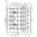
- FIG. 3A is a diagram showing an example of a plan view of a radio frequency power amplifier 300 according to embodiment 3.
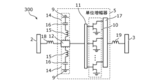
- FIG. 3B is a diagram showing an example of an equivalent circuit diagram of the radio frequency power amplifier 300 according to embodiment 3.
- the radio frequency power amplifier 300 according to embodiment 3 has a configuration in which there are multiple shunt circuits 14 per unit amplifier 5 in the radio frequency power amplifier 100 according to embodiment 1, or a configuration in which there are multiple shunt circuits 14 per unit amplifier 5 in the radio frequency power amplifier 200 according to embodiment 2.
- the following describes the radio frequency power amplifier device 300 according to the third embodiment, taking as an example a case where the radio frequency power amplifier device 100 according to the first embodiment is used as a base, and focuses on the differences from the radio frequency power amplifier device 100 according to the first embodiment.
- the shunt circuit 14 is connected to the gate side of the RF transistor 10, the impedance of the shunt circuit 14 must also be reduced in order to reduce losses. Therefore, as in this embodiment, by providing multiple shunt circuits 14 for each unit amplifier 5, it is possible to reduce the impedance while keeping the resonant frequency constant.
- the radio frequency power amplifier 300 according to the third embodiment has multiple shunt circuits 14 per unit amplifier 5 in the radio frequency power amplifier 100 according to the first embodiment or the radio frequency power amplifier 200 according to the second embodiment, and the resonant frequencies of the multiple shunt circuits 14 are equal.
- Figures 3A and 3B show a case where there is one unit amplifier 5, there may be multiple unit amplifiers 5. In other words, there may be multiple unit amplifiers 5, and multiple shunt circuits 14 may be provided for each of the multiple unit amplifiers 5.
- the inductance of the semiconductor inductor 15 and the capacitance of the MIM capacitor 16 may be different as long as their resonant frequencies are the same.
- FIG. 4A is a diagram showing an example of a plan view of a high frequency power amplifier 400 according to embodiment 4.
- FIG. 4B is a diagram showing an example of an equivalent circuit diagram of the high frequency power amplifier 400 according to embodiment 4.
- the high frequency power amplifier 400 according to embodiment 4 has a configuration in which a resistive element 22, which is an example of an impedance element including a resistive component that connects two shunt circuits 14, is added to the high frequency power amplifier 300 according to embodiment 3. Note that, in the example shown in FIGS. 4A and 4B, a case will be described in which there is one unit amplifier 5 and multiple shunt circuits 14 in the unit amplifier 5.
- the following describes the radio frequency power amplifier device 400 according to the fourth embodiment, focusing on the differences from the radio frequency power amplifier device 300 according to the third embodiment.
- connection point between the semiconductor inductor 15 and the MIM capacitance 16 in one shunt circuit 14 and the connection point between the semiconductor inductor 15 and the MIM capacitance 16 in another shunt circuit 14 are electrically connected using a resistive element 22, which is an example of an impedance element that includes a resistive component.
- resistive element 22 is used as the impedance element that includes a resistive component in Figures 4A and 4B, other impedance elements that include a resistive component may also be used.
- FIG. 4C is a diagram showing another example of a plan view of the high frequency power amplifier device 400 according to embodiment 4 (i.e., an example of a plan view of the high frequency power amplifier device 400a).
- FIG. 4D is a diagram showing another example of an equivalent circuit diagram of the high frequency power amplifier device 400 according to embodiment 4 (i.e., an example of an equivalent circuit diagram of the high frequency power amplifier device 400a).
- connection point between the semiconductor inductor 15 and the MIM capacitance 16 in one shunt circuit 14 and the connection point between the semiconductor inductor 15 and the MIM capacitance 16 in another shunt circuit 14 are electrically connected using a resistive element 22, which is an example of an impedance element including a resistance component, and a capacitor 23, which is an example of a DC blocking element connected in series with the resistive element 22.
- a resistive element 22 which is an example of an impedance element including a resistance component
- a capacitor 23 which is an example of a DC blocking element connected in series with the resistive element 22.
- FIG. 4E is a diagram showing another example of a plan view of the high frequency power amplifier device 400 according to embodiment 4 (i.e., an example of a plan view of the high frequency power amplifier device 400b).
- FIG. 4F is a diagram showing another example of an equivalent circuit diagram of the high frequency power amplifier device 400 according to embodiment 4 (i.e., an example of an equivalent circuit diagram of the high frequency power amplifier device 400b).
- connection point between the semiconductor inductor 15 and the MIM capacitor 16 in one shunt circuit 14 and the connection point between the semiconductor inductor 15 and the MIM capacitor 16 in another shunt circuit 14 are shorted by a short circuit wiring 24 on the semiconductor substrate 4, and further, a resistive element 22, which is an example of an impedance element including a resistive component, and a capacitor 23, which is an example of a DC blocking element connected in series with the resistive element 22, are connected between the short circuit wiring 24 and the ground via 9.
- the connection points of the two shunt circuits 14 are shorted together, but these connection points have an impedance with respect to the ground potential that corresponds to the series connection of the resistive element 22 and the capacitor 23.
- FIG. 5A is a diagram showing another example of a plan view of the radio frequency power amplifier 400 according to embodiment 4 (i.e., an example of a plan view of the radio frequency power amplifier 400c).
- FIG. 5B is a diagram showing another example of an equivalent circuit diagram of the radio frequency power amplifier 400 according to embodiment 4 (i.e., an example of an equivalent circuit diagram of the radio frequency power amplifier 400c).
- the radio frequency power amplifier 400c there are multiple unit amplifiers 5 and one shunt circuit 14 in the unit amplifier 5.
- the following describes the high frequency power amplifier device 400c, focusing on the differences from the high frequency power amplifier device 100 according to embodiment 1.
- connection point between the semiconductor inductor 15 and the MIM capacitance 16 in one shunt circuit 14 and the connection point between the semiconductor inductor 15 and the MIM capacitance 16 in another shunt circuit 14 are electrically connected to each other.
- a resistive element 22 is used as an impedance element that includes a resistive component, but other impedance elements that include a resistive component may also be used.
- the connection point between the semiconductor inductor 15 and the MIM capacitance 16 in the shunt circuit 14 and the connection point between the semiconductor inductor 15 and the MIM capacitance 16 in another shunt circuit 14 are connected by an impedance element to average out the variations in the resonant frequency caused by manufacturing variations and prevent the impedance from becoming high at a particular frequency.
- a typical value of the resistor element 22, which is an example of an impedance element, is about 5 ⁇ to 50 ⁇ .
- the radio frequency power amplifier devices 400 to 400c according to the fourth embodiment include, in addition to the configuration of the radio frequency power amplifier device 300 according to the third embodiment, an impedance element including a resistance component that electrically connects the connection point between the semiconductor inductor 15 and the MIM capacitance 16 included in one of the multiple shunt circuits 14 and the connection point between the semiconductor inductor 15 and the MIM capacitance 16 included in another of the multiple shunt circuits 14.
- the impedance element may also serve to prevent loop oscillation, similar to the resistors connected between the gate bus lines 11 and/or between the drain bus lines 17 of the multiple unit amplifiers 5 described in embodiment 1.
- the radio frequency power amplifier according to the fifth embodiment corresponds to an example characterized by the layout on the gate side of the RF transistor 10 in the radio frequency power amplifier 100 according to the first embodiment or the radio frequency power amplifier 200 according to the second embodiment.
- FIG. 6 is an example of an enlarged plan view of the gate side of the RF transistor 10 of the high frequency power amplifier device 100 according to embodiment 5.
- Each of the multiple input bonding pads 12 is connected to a gate bus line 11. There are multiple input bonding pads 12 (three in FIG. 6), and they are arranged at regular intervals.
- Each of the two connection parts 13 connects adjacent input bonding pads 12 together.
- connection parts 13 are the same metal layer as the input bonding pads 12 (i.e., they are formed from the same material and in the same manufacturing process). For this reason, the two connection parts 13 are the same as the multiple input bonding pads 12 in at least one of the thickness, material, and height position from the bottom surface of the semiconductor substrate 4.
- the width (shown as A in FIG. 6) of each of the two connection portions 13 is shorter than the length (shown as B in FIG. 6) of the input bonding pad 12.
- the minimum dimension of the width A of the connection portion 13 is the minimum value of the design rules for the semiconductor process (e.g., about 5 ⁇ m), and the maximum dimension is the length B of the input bonding pad 12 (e.g., about 100 ⁇ m).
- input bonding pads are sometimes combined into one without being divided into multiple pads as shown in FIG. 6.
- the area of each bonding pad can be made smaller than when combined into one pad, and therefore the parasitic capacitance can be reduced.
- connection parts 13 were not present, the potential of the radio frequency signal coming into the three input bonding pads 12 via the input wires (not shown) would vary for each input bonding pad 12 and would not be constant, which would cause the RF transistor 10 to operate unevenly. Therefore, in this embodiment, the three input bonding pads 12 are connected by two connection parts 13, the potential of the radio frequency signal is made uniform on the three input bonding pads 12, and then the DC voltage and radio frequency voltage to each finger of the RF transistor 10 are made uniform, thereby enabling uniform amplification operation.
- the unit amplifier 5 has a plurality of input bonding pads 12, and the unit amplifier 5 further has a connection portion 13 that connects two adjacent input bonding pads 12 of the plurality of input bonding pads 12, and the connection portion 13 has the same thickness, material, and at least one of the height positions from the bottom surface of the semiconductor substrate 4 as the plurality of input bonding pads 12, and in the direction perpendicular to the gate bus line 11, the width of the connection portion 13 is shorter than the length of the plurality of input bonding pads 12.
- each input bonding pad 12 can be made smaller than when the individual input bonding pads 12 are combined into one, thereby reducing the associated parasitic capacitance and reducing input-side losses, i.e., suppressing deterioration of the gain and efficiency of the high frequency power amplifier 100. This is particularly effective when the operating frequency is high.
- connection part 13 is gold, aluminum, or copper, but is not limited to these.
- the radio frequency power amplifier according to the sixth embodiment corresponds to an example in which the layout of the shunt circuit 14 in the radio frequency power amplifier 100 according to the first embodiment or the radio frequency power amplifier 200 according to the second embodiment is modified.
- FIG. 7A shows another example of an equivalent circuit diagram of the shunt circuit 14 of the high frequency power amplifier device 100 according to embodiment 1, as an example of embodiment 6.
- the input bonding pad 12 is connected in series with the semiconductor inductor 15, the MIM capacitor 16, and the ground via 9, in that order
- the shunt circuit 14 is connected in series with the input bonding pad 12, the MIM capacitor 16, the semiconductor inductor 15, and the ground via 9, in that order.
- FIG. 7B is a diagram showing an example of a plan view of the shunt circuit 14 in FIG. 7A.
- the input bonding pad 12 and the connection portion 13 are arranged so as to overlap the MIM capacitance 16 in a top view.
- the MIM capacitance 16 is arranged below the input bonding pad 12 in a cross-sectional view of the high frequency power amplifier device 100.
- the input bonding pad 12 and/or the connection portion 13 are electrically conductive with the upper electrode of the MIM capacitance 16.
- One end of the semiconductor inductor 15 is connected to the lower electrode of the MIM capacitor 16, and the other end is connected to the ground via 9 via the semiconductor inductor lead-out wiring 49.
- the ground via 9 penetrates the semiconductor substrate 4 and provides electrical continuity between the ground terminals on the top and bottom surfaces of the semiconductor substrate 4.
- FIG. 7C is an example of a cross-sectional structure diagram taken along line D-D' in FIG. 7B.
- the input bonding pad 12 and the semiconductor inductor 15 are formed from the same metal layer (i.e., the same material and the same manufacturing process).
- the MIM capacitance lower electrode 43 is directly connected to one end of the semiconductor inductor 15 through an opening in the interlayer film 42.
- the MIM capacitance upper electrode 44 is directly connected to the input bonding pad 12 through an opening in the interlayer film 42.
- the other end of the semiconductor inductor 15 is connected to the ground via 9 through a semiconductor inductor lead-out wiring 49 (not shown).
- the semiconductor inductor lead-out wiring 49 is formed from a different metal layer (i.e., a different manufacturing process) from the semiconductor inductor 15. For example, the same metal layer as the MIM capacitance lower electrode 43 may be used.
- the ground via 9 penetrates the semiconductor substrate 4 and provides electrical conductivity between the top and bottom ground terminals of the semiconductor substrate 4 (not shown).
- FIG. 7D is a diagram showing another example of a plan view of the shunt circuit 14 in FIG. 7A (i.e., FIG. 7B). The difference from FIG. 7B is that, when viewed from above, not only the input bonding pad 12 and the connection portion 13 but also the semiconductor inductor 15 overlaps with the MIM capacitance 16.
- the input bonding pad 12 and the connection portion 13 are arranged so as to overlap the MIM capacitance 16 in a top view.
- the input bonding pad 12 and/or the connection portion 13 are electrically conductive with the lower electrode of the MIM capacitance 16.
- the semiconductor inductor 15 is arranged so as to overlap the MIM capacitance 16 in a top view. One end is connected to the upper electrode of the MIM capacitance 16, and the other end is connected to the ground via 9.
- the ground via 9 penetrates the semiconductor substrate 4 and provides electrical continuity between the ground terminals on the top and bottom surfaces of the semiconductor substrate 4.
- FIG. 7E is a diagram showing an example of a cross-sectional structure diagram taken along the line D-D' in FIG. 7D.
- the input bonding pad 12 and the semiconductor inductor 15 are formed of different metal layers.
- the MIM capacitance lower electrode 43 is directly connected to the input bonding pad 12 through the openings in the interlayer film 42 and the first protective film 46.
- the MIM capacitance upper electrode 44 is directly connected to one end of the semiconductor inductor 15 through the opening in the interlayer film 42.
- the other end of the semiconductor inductor 15 is connected to the ground via 9.
- the ground via 9 penetrates the semiconductor substrate 4 and provides electrical continuity between the ground terminals on the top and bottom surfaces of the semiconductor substrate 4.
- FIG. 7F is a diagram showing another example of a cross-sectional structure diagram taken along the line D-D' in FIG. 7D.
- the difference from FIG. 7E is that the semiconductor inductor 15 is formed below the MIM capacitor lower electrode 43 of the MIM capacitor 16 in the cross-sectional view.
- the input bonding pad 12 and the semiconductor inductor 15 are formed from different metal layers.
- the MIM capacitance lower electrode 43 is directly connected to one end of the semiconductor inductor 15 through an opening in the interlayer film 42.
- the MIM capacitance upper electrode 44 is directly connected to the input bonding pad 12 through an opening in the interlayer film 42.
- the other end of the semiconductor inductor 15 is connected to the ground via 9.
- the ground via 9 penetrates the semiconductor substrate 4 and provides electrical continuity between the ground terminals on the top and bottom surfaces of the semiconductor substrate 4.
- connection order of the semiconductor inductor 15 and MIM capacitor 16 of the shunt circuit 14 from the input bonding pad 12 has the same characteristics in both DC and high frequency.
- the input bonding pad 12 and the MIM capacitor 16 overlap, so the area they occupy on the semiconductor substrate 4 can be made smaller than when they do not overlap.
- the MIM capacitance 16 and the semiconductor inductor 15 are connected in order from the side closest to the input bonding pad 12, and the MIM capacitance 16 overlaps with the input bonding pad 12 in a top view of the radio frequency power amplifier device 100, and the MIM capacitance 16 is disposed below the input bonding pad 12 in a cross-sectional view of the radio frequency power amplifier device 100.
- the MIM capacitor 16 is arranged so as to overlap under the input bonding pad 12, and compared to a case in which they do not overlap, the chip area of the high frequency power amplifier can be reduced, which can contribute to reducing the cost of the semiconductor chip as the high frequency power amplifier.
- the input bonding pad 12 does not protrude from the MIM capacitor 16 when viewed from above, but it is acceptable for a portion of it to protrude.
- FIG. 8A is a diagram showing an example of a plan view of a radio frequency power amplifier device 500 according to embodiment 7.
- the radio frequency power amplifier device 500 according to embodiment 7 has a configuration in which a shield metal layer 47 and the like are added to the radio frequency power amplifier device 100 according to embodiment 1 or the radio frequency power amplifier device 200 according to embodiment 2.
- the following describes the radio frequency power amplifier device 500 according to embodiment 7, taking as an example a case where the radio frequency power amplifier device 100 according to embodiment 1 is used as a base, and focuses on the differences from the radio frequency power amplifier device 100 according to embodiment 1.
- FIG. 8B is a diagram showing an example of a cross-sectional structure diagram of a high-frequency power amplifier device 500 according to embodiment 7, cut along an extension line (indicated by C-C') of the portion where the input wire 18 and the semiconductor inductor 15 overlap in FIG. 8A.
- a first wiring pattern 2 and a semiconductor substrate 4 are mounted on the main surface of the submount substrate 1.
- the semiconductor substrate 4 is composed of a silicon substrate 41, an interlayer film 42, a first protective film 46, and a second protective film 48.
- One end of the semiconductor inductor 15 is connected to the input bonding pad 12, and the other end is connected to the semiconductor inductor lead-out wiring 49.
- the MIM capacitor 16 is composed of a MIM capacitor lower electrode 43 and a MIM capacitor upper electrode 44, and is formed between the interlayer films 42.
- the wiring 45 connects the MIM capacitor upper electrode 44 and the semiconductor inductor lead wiring 49.
- the MIM capacitor lower electrode 43 is connected to the ground via 9 (not shown in FIG. 8B).
- the input bonding pad 12, the semiconductor inductor 15, the drain finger 8, and the wiring 45 are formed on the interlayer film 42.
- the input bonding pad 12, the semiconductor inductor 15, the drain finger 8, and the wiring 45 are formed from the same metal layer.
- the shield metal layer 47 is disposed in contact with the first protective film 46, and is disposed between the semiconductor inductor 15 and the MIM capacitor 16 and the input wire 18 in a cross-sectional view.
- a second protective film 48 made of polyimide or the like is disposed on top of the shield metal layer 47 to protect the shield metal layer.
- the shield metal layer 47 is formed of a metal layer different from the input bonding pad 12. Therefore, the shield metal layer 47 differs from the input bonding pad 12 in at least one of the thickness, material, and height position from the bottom surface of the semiconductor substrate 4.
- the shield metal layer 47 is connected to a ground potential through a ground via (not shown) on the semiconductor substrate 4.
- FIG. 8C is a diagram showing another example of a cross-sectional structure diagram of the high frequency power amplifier device 500 according to embodiment 7 taken along the C-C' cutting line in FIG. 8A (i.e., an example of a cross-sectional structure diagram of the high frequency power amplifier device 500a).
- the shield metal layer 47 is formed from the same metal layer as the input bonding pad 12, and the first protective film 46 also serves as a protective film for the shield metal layer 47.
- the shield metal layer 47 is the same as the input bonding pad 12 in at least one of the thickness, material, and height position from the bottom surface of the semiconductor substrate 4.
- the MIM capacitance upper electrode 44 is connected to the ground via 9 (not shown), and the MIM capacitance lower electrode 43 is connected to one end of the semiconductor inductor 15.
- the semiconductor inductor 15 and the input wire 18 are each equivalent to an inductor, and possible means of suppressing interference between the inductors include 1) making sure they do not overlap when viewed from above, 2) keeping them apart when viewed from above, and 3) placing a shield between them.
- 1) and 2) are difficult to achieve, and 3) placing a shield between them is the most effective and efficient method.
- the high frequency power amplifier 500 according to the seventh embodiment further includes a shield metal layer 47 mounted on the semiconductor substrate 4 in the high frequency power amplifier 100 according to the first embodiment or the high frequency power amplifier 200 according to the second embodiment, and the shield metal layer 47 (1) is formed in a region including the semiconductor inductor 15 and the MIM capacitor 16 in a top view of the high frequency power amplifier 100, (2) is disposed between the multiple input wires 18 and the shunt circuit 14 and is grounded in a cross-sectional view of the high frequency power amplifier 100, (3) is different from the input bonding pad 12 in at least one of the thickness, material, and height position from the bottom surface of the semiconductor substrate 4, and (4) has a second protective film 48 covering the upper part of the shield metal layer 47, and the multiple input wires 18 overlap the shunt circuit 14 in a top view.
- the radio frequency power amplifier 500a according to the seventh embodiment is the radio frequency power amplifier 100 according to the first embodiment or the radio frequency power amplifier 200 according to the second embodiment, further comprising a shield metal layer 47 mounted on the semiconductor substrate 4, the shield metal layer 47 being (1) formed in a region including the semiconductor inductor 15 and the MIM capacitance 16 in a top view of the radio frequency power amplifier 100, (2) disposed between the multiple input wires 18 and the shunt circuit 14 and grounded in a cross-sectional view of the radio frequency power amplifier 100, (3) having the same thickness, material, and at least one of the height position from the bottom surface of the semiconductor substrate 4 as the input bonding pad 12, and (4) having a second protective film 48 covering the upper part of the shield metal layer 47, and the multiple input wires 18 overlap with the shunt circuit 14 in a top view.
- the shield metal layer 47 may be left floating without being fixed at a fixed potential.
- the MIM capacitance upper electrode 44 is connected to the wiring 45, and the MIM capacitance lower electrode 43 is connected to the ground via 9, but the connections may be reversed.
- the MIM capacitance upper electrode 44 is connected to the ground via 9
- the MIM capacitance lower electrode 43 is connected to the semiconductor inductor 15, but the connections may be reversed.
- FIG. 9 is a diagram showing an example of a plan view of a high frequency power amplifier 600 according to embodiment 8.
- the high frequency power amplifier 600 according to embodiment 8 corresponds to an example in which the resonant frequency of the shunt circuit 14 in the high frequency power amplifier 100 according to embodiment 1 or the high frequency power amplifier 200 according to embodiment 2 is limited to a specific value.
- the following describes the radio frequency power amplifier device 600 according to embodiment 8, taking as an example a case where the device is configured based on the radio frequency power amplifier device 200 according to embodiment 2, focusing on the differences from the radio frequency power amplifier device 200 according to embodiment 2.
- submount substrate 1, the drain bus line 17, the multiple input wires 18, and the multiple output wires 19 are not essential components.
- the high-frequency signal is input to the unit amplifier 5 from the first wiring pattern 2 via three input wires 18. After being amplified by the unit amplifier 5, the high-frequency signal is output from the second wiring pattern 3 via two output wires 19.
- the frequency (f0) of the fundamental signal is a frequency within the band of the fundamental signal amplified by the high frequency power amplifier 600 (for example, 3.3 GHz to 3.8 GHz).
- the resonant frequency fr of the shunt circuit 14 is set equal to half the frequency f0/2 of the fundamental signal, and at f0/2, the shunt circuit 14 is shorted in terms of impedance (i.e., in a short-circuit state) to reduce the effect on the fundamental signal.
- f0 3.55 GHz
- f0/2 1.775 GHz
- the capacitance of the MIM capacitor 16 is 20 pF
- the inductance of the semiconductor inductor 15 is about 0.40 nH.
- the configuration is based on the high frequency power amplifier 200 according to embodiment 2 (i.e., when there is one unit amplifier 5) has been described, but the configuration may also be based on the high frequency power amplifier 100 according to embodiment 1 (i.e., there may be multiple unit amplifiers 5). In this case, a closed loop can be formed between multiple unit amplifiers, so a similar effect can be expected.
- the ninth embodiment corresponds to another design example of the shunt circuit 14 in the eighth embodiment. Therefore, the configuration of the radio frequency power amplifier device according to the ninth embodiment is similar to that of the radio frequency power amplifier device 600 according to the eighth embodiment shown in FIG.
- the following describes the radio frequency power amplifier device according to embodiment 9, focusing on the differences from the radio frequency power amplifier device 600 according to embodiment 8.
- the resonant frequency of the shunt circuit must be designed to be outside the band of the fundamental signal amplified by the high frequency power amplifier. This is because the impedance at the resonant frequency of the shunt circuit is shorted (i.e., short-circuited), and the signal does not pass through.
- the resonant frequency fr of the shunt circuit should be set at least n times (n is a real number) the signal bandwidth BW away from the lower limit frequency fl or the upper limit frequency fu within the band of the fundamental signal.
- n may be 1 or more.
- n may be 2 or more.
- the shunt circuit 14 is designed to satisfy the above conditions.
- frl is 2.3 GHz or less and fru is 4.8 GHz or more.
- the capacitance of MIM capacitor 16 is 20 pF, then the inductance of semiconductor inductor 15 is approximately 0.24 nH or more, or 0.06 nH or less.
- the features of the high frequency power amplifier device according to the eighth embodiment may be added to the configuration of the high frequency power amplifier device according to the ninth embodiment.
- the high frequency power amplifier device has been described above based on the embodiments, but the present disclosure is not limited to these embodiments. As long as it does not deviate from the gist of the present disclosure, various modifications conceivable by a person skilled in the art to the present embodiments and other forms constructed by combining some of the components in the embodiments are also included within the scope of the present disclosure.
- the radio frequency power amplifier device may be a radio frequency power amplifier device having the features of two or more forms selected from embodiments 3 to 9 in addition to the radio frequency power amplifier device of embodiment 1 or 2. Even in such a form, since it has at least the features of the radio frequency power amplifier device of embodiment 1 or 2, a radio frequency power amplifier device is realized that can reduce the effects of wire length variations by using multiple input wires and suppress variations in high frequency characteristics such as gain within a semiconductor substrate and variations between radio frequency power amplifier devices.
- the high frequency power amplifier device disclosed herein can be used as an amplifier device installed in wireless communication base stations used in the microwave and millimeter wave bands.
Landscapes
- Engineering & Computer Science (AREA)
- Power Engineering (AREA)
- Physics & Mathematics (AREA)
- Nonlinear Science (AREA)
- Microelectronics & Electronic Packaging (AREA)
- Amplifiers (AREA)
Priority Applications (1)
| Application Number | Priority Date | Filing Date | Title |
|---|---|---|---|
| JP2025510731A JPWO2024203872A1 (https=) | 2023-03-29 | 2024-03-22 |
Applications Claiming Priority (4)
| Application Number | Priority Date | Filing Date | Title |
|---|---|---|---|
| US202363492956P | 2023-03-29 | 2023-03-29 | |
| US63/492,956 | 2023-03-29 | ||
| US202363493214P | 2023-03-30 | 2023-03-30 | |
| US63/493,214 | 2023-03-30 |
Publications (1)
| Publication Number | Publication Date |
|---|---|
| WO2024203872A1 true WO2024203872A1 (ja) | 2024-10-03 |
Family
ID=92905036
Family Applications (2)
| Application Number | Title | Priority Date | Filing Date |
|---|---|---|---|
| PCT/JP2024/011341 Ceased WO2024203872A1 (ja) | 2023-03-29 | 2024-03-22 | 高周波電力増幅装置 |
| PCT/JP2024/011317 Ceased WO2024203860A1 (ja) | 2023-03-29 | 2024-03-22 | 高周波増幅器 |
Family Applications After (1)
| Application Number | Title | Priority Date | Filing Date |
|---|---|---|---|
| PCT/JP2024/011317 Ceased WO2024203860A1 (ja) | 2023-03-29 | 2024-03-22 | 高周波増幅器 |
Country Status (3)
| Country | Link |
|---|---|
| US (1) | US20260012144A1 (https=) |
| JP (2) | JPWO2024203860A1 (https=) |
| WO (2) | WO2024203872A1 (https=) |
Citations (4)
| Publication number | Priority date | Publication date | Assignee | Title |
|---|---|---|---|---|
| JP2008109227A (ja) * | 2006-10-23 | 2008-05-08 | Mitsubishi Electric Corp | 高周波電力増幅器 |
| JP2010161348A (ja) * | 2008-12-10 | 2010-07-22 | Toshiba Corp | 高周波半導体装置 |
| WO2016203644A1 (ja) * | 2015-06-19 | 2016-12-22 | 三菱電機株式会社 | 電力増幅器 |
| JP2022089147A (ja) * | 2020-12-03 | 2022-06-15 | エヌエックスピー ユーエスエイ インコーポレイテッド | パワートランジスタと静電放電保護回路とを別々の基板に搭載した電力増幅器 |
Family Cites Families (5)
| Publication number | Priority date | Publication date | Assignee | Title |
|---|---|---|---|---|
| US4406991A (en) * | 1982-02-04 | 1983-09-27 | Westinghouse Electric Corp. | High power resonance filters |
| JPH0512795A (ja) * | 1991-07-02 | 1993-01-22 | Sony Corp | ハーフトラツプ回路 |
| JP3888785B2 (ja) * | 1998-09-28 | 2007-03-07 | 三菱電機株式会社 | 高周波電力増幅器 |
| JP2002171138A (ja) * | 2000-12-01 | 2002-06-14 | Nec Corp | マイクロ波電力増幅器 |
| JP5571047B2 (ja) * | 2011-09-15 | 2014-08-13 | 株式会社東芝 | 電力増幅装置 |
-
2024
- 2024-03-22 WO PCT/JP2024/011341 patent/WO2024203872A1/ja not_active Ceased
- 2024-03-22 JP JP2025510722A patent/JPWO2024203860A1/ja active Pending
- 2024-03-22 JP JP2025510731A patent/JPWO2024203872A1/ja active Pending
- 2024-03-22 WO PCT/JP2024/011317 patent/WO2024203860A1/ja not_active Ceased
-
2025
- 2025-09-15 US US19/328,335 patent/US20260012144A1/en active Pending
Patent Citations (4)
| Publication number | Priority date | Publication date | Assignee | Title |
|---|---|---|---|---|
| JP2008109227A (ja) * | 2006-10-23 | 2008-05-08 | Mitsubishi Electric Corp | 高周波電力増幅器 |
| JP2010161348A (ja) * | 2008-12-10 | 2010-07-22 | Toshiba Corp | 高周波半導体装置 |
| WO2016203644A1 (ja) * | 2015-06-19 | 2016-12-22 | 三菱電機株式会社 | 電力増幅器 |
| JP2022089147A (ja) * | 2020-12-03 | 2022-06-15 | エヌエックスピー ユーエスエイ インコーポレイテッド | パワートランジスタと静電放電保護回路とを別々の基板に搭載した電力増幅器 |
Also Published As
| Publication number | Publication date |
|---|---|
| WO2024203860A1 (ja) | 2024-10-03 |
| JPWO2024203860A1 (https=) | 2024-10-03 |
| JPWO2024203872A1 (https=) | 2024-10-03 |
| US20260012144A1 (en) | 2026-01-08 |
Similar Documents
| Publication | Publication Date | Title |
|---|---|---|
| EP1573813B1 (en) | Rf power transistor with internal bias feed | |
| US7511575B2 (en) | High-frequency power amplifier | |
| KR102632903B1 (ko) | 트랜지스터 레벨 입력 및 출력 고조파 종단들 | |
| CN108233881B (zh) | 放大器电路和经封装的放大器电路 | |
| US8786369B2 (en) | High frequency amplifier | |
| CN109643976B (zh) | 具有高功率密度的封装射频功率放大器 | |
| US9711466B2 (en) | Electronic apparatus operable in high frequencies | |
| US8633527B2 (en) | Semiconductor device having first and second resistance for suppressing loop oscillation | |
| US11322462B2 (en) | Semiconductor device | |
| EP4352786A1 (en) | Packaged transistor amplifier with integrated passive device matching structure having distributed shunt inductances | |
| TWI766337B (zh) | 半導體裝置 | |
| JP2017103678A (ja) | 高周波半導体増幅器 | |
| CN105390234B (zh) | 变压器 | |
| JP7239023B2 (ja) | 高周波半導体装置 | |
| EP3847696B1 (en) | Power amplifier with decreased rf return current losses | |
| WO2014207498A1 (en) | High frequency amplifier | |
| WO2024203872A1 (ja) | 高周波電力増幅装置 | |
| US20220293550A1 (en) | Semiconductor device | |
| US10707818B1 (en) | RF amplifier with impedance matching components monolithically integrated in transistor die | |
| JP2012099609A (ja) | 高周波半導体装置 | |
| US20240145414A1 (en) | Rf amplifiers with improved stability by source inductance adjustment | |
| EP4297274A1 (en) | Flip chip doherty amplifier devices | |
| US20250219586A1 (en) | Doherty amplifier | |
| JP4547823B2 (ja) | 高周波モジュール | |
| CN118648235A (zh) | 具有提高的视频带宽的紧凑型多赫蒂放大器 |
Legal Events
| Date | Code | Title | Description |
|---|---|---|---|
| 121 | Ep: the epo has been informed by wipo that ep was designated in this application |
Ref document number: 24779990 Country of ref document: EP Kind code of ref document: A1 |
|
| ENP | Entry into the national phase |
Ref document number: 2025510731 Country of ref document: JP Kind code of ref document: A |
|
| WWE | Wipo information: entry into national phase |
Ref document number: 2025510731 Country of ref document: JP |
|
| NENP | Non-entry into the national phase |
Ref country code: DE |
|
| 122 | Ep: pct application non-entry in european phase |
Ref document number: 24779990 Country of ref document: EP Kind code of ref document: A1 |