WO2024203110A1 - 半導体装置、および半導体装置の製造方法 - Google Patents
半導体装置、および半導体装置の製造方法 Download PDFInfo
- Publication number
- WO2024203110A1 WO2024203110A1 PCT/JP2024/008720 JP2024008720W WO2024203110A1 WO 2024203110 A1 WO2024203110 A1 WO 2024203110A1 JP 2024008720 W JP2024008720 W JP 2024008720W WO 2024203110 A1 WO2024203110 A1 WO 2024203110A1
- Authority
- WO
- WIPO (PCT)
- Prior art keywords
- semiconductor device
- terminal
- sealing resin
- semiconductor element
- protrusion
- Prior art date
- Legal status (The legal status is an assumption and is not a legal conclusion. Google has not performed a legal analysis and makes no representation as to the accuracy of the status listed.)
- Ceased
Links
Images











Classifications
-
- H—ELECTRICITY
- H10—SEMICONDUCTOR DEVICES; ELECTRIC SOLID-STATE DEVICES NOT OTHERWISE PROVIDED FOR
- H10W—GENERIC PACKAGES, INTERCONNECTIONS, CONNECTORS OR OTHER CONSTRUCTIONAL DETAILS OF DEVICES COVERED BY CLASS H10
- H10W74/00—Encapsulations, e.g. protective coatings
- H10W74/01—Manufacture or treatment
- H10W74/016—Manufacture or treatment using moulds
-
- H—ELECTRICITY
- H10—SEMICONDUCTOR DEVICES; ELECTRIC SOLID-STATE DEVICES NOT OTHERWISE PROVIDED FOR
- H10W—GENERIC PACKAGES, INTERCONNECTIONS, CONNECTORS OR OTHER CONSTRUCTIONAL DETAILS OF DEVICES COVERED BY CLASS H10
- H10W42/00—Arrangements for protection of devices
- H10W42/121—Arrangements for protection of devices protecting against mechanical damage
-
- H—ELECTRICITY
- H10—SEMICONDUCTOR DEVICES; ELECTRIC SOLID-STATE DEVICES NOT OTHERWISE PROVIDED FOR
- H10W—GENERIC PACKAGES, INTERCONNECTIONS, CONNECTORS OR OTHER CONSTRUCTIONAL DETAILS OF DEVICES COVERED BY CLASS H10
- H10W70/00—Package substrates; Interposers; Redistribution layers [RDL]
- H10W70/01—Manufacture or treatment
- H10W70/04—Manufacture or treatment of leadframes
- H10W70/041—Connecting or disconnecting interconnections to or from leadframes, e.g. connecting bond wires or bumps
-
- H—ELECTRICITY
- H10—SEMICONDUCTOR DEVICES; ELECTRIC SOLID-STATE DEVICES NOT OTHERWISE PROVIDED FOR
- H10W—GENERIC PACKAGES, INTERCONNECTIONS, CONNECTORS OR OTHER CONSTRUCTIONAL DETAILS OF DEVICES COVERED BY CLASS H10
- H10W70/00—Package substrates; Interposers; Redistribution layers [RDL]
- H10W70/01—Manufacture or treatment
- H10W70/04—Manufacture or treatment of leadframes
- H10W70/042—Etching
-
- H—ELECTRICITY
- H10—SEMICONDUCTOR DEVICES; ELECTRIC SOLID-STATE DEVICES NOT OTHERWISE PROVIDED FOR
- H10W—GENERIC PACKAGES, INTERCONNECTIONS, CONNECTORS OR OTHER CONSTRUCTIONAL DETAILS OF DEVICES COVERED BY CLASS H10
- H10W70/00—Package substrates; Interposers; Redistribution layers [RDL]
- H10W70/40—Leadframes
- H10W70/411—Chip-supporting parts, e.g. die pads
- H10W70/415—Leadframe inner leads serving as die pads
-
- H—ELECTRICITY
- H10—SEMICONDUCTOR DEVICES; ELECTRIC SOLID-STATE DEVICES NOT OTHERWISE PROVIDED FOR
- H10W—GENERIC PACKAGES, INTERCONNECTIONS, CONNECTORS OR OTHER CONSTRUCTIONAL DETAILS OF DEVICES COVERED BY CLASS H10
- H10W70/00—Package substrates; Interposers; Redistribution layers [RDL]
- H10W70/40—Leadframes
- H10W70/421—Shapes or dispositions
- H10W70/424—Cross-sectional shapes
-
- H—ELECTRICITY
- H10—SEMICONDUCTOR DEVICES; ELECTRIC SOLID-STATE DEVICES NOT OTHERWISE PROVIDED FOR
- H10W—GENERIC PACKAGES, INTERCONNECTIONS, CONNECTORS OR OTHER CONSTRUCTIONAL DETAILS OF DEVICES COVERED BY CLASS H10
- H10W70/00—Package substrates; Interposers; Redistribution layers [RDL]
- H10W70/40—Leadframes
- H10W70/464—Additional interconnections in combination with leadframes
- H10W70/468—Circuit boards
-
- H—ELECTRICITY
- H10—SEMICONDUCTOR DEVICES; ELECTRIC SOLID-STATE DEVICES NOT OTHERWISE PROVIDED FOR
- H10W—GENERIC PACKAGES, INTERCONNECTIONS, CONNECTORS OR OTHER CONSTRUCTIONAL DETAILS OF DEVICES COVERED BY CLASS H10
- H10W72/00—Interconnections or connectors in packages
-
- H—ELECTRICITY
- H10—SEMICONDUCTOR DEVICES; ELECTRIC SOLID-STATE DEVICES NOT OTHERWISE PROVIDED FOR
- H10W—GENERIC PACKAGES, INTERCONNECTIONS, CONNECTORS OR OTHER CONSTRUCTIONAL DETAILS OF DEVICES COVERED BY CLASS H10
- H10W74/00—Encapsulations, e.g. protective coatings
- H10W74/01—Manufacture or treatment
-
- H—ELECTRICITY
- H10—SEMICONDUCTOR DEVICES; ELECTRIC SOLID-STATE DEVICES NOT OTHERWISE PROVIDED FOR
- H10W—GENERIC PACKAGES, INTERCONNECTIONS, CONNECTORS OR OTHER CONSTRUCTIONAL DETAILS OF DEVICES COVERED BY CLASS H10
- H10W74/00—Encapsulations, e.g. protective coatings
- H10W74/10—Encapsulations, e.g. protective coatings characterised by their shape or disposition
- H10W74/111—Encapsulations, e.g. protective coatings characterised by their shape or disposition the semiconductor body being completely enclosed
- H10W74/129—Encapsulations, e.g. protective coatings characterised by their shape or disposition the semiconductor body being completely enclosed forming a chip-scale package [CSP]
-
- H—ELECTRICITY
- H10—SEMICONDUCTOR DEVICES; ELECTRIC SOLID-STATE DEVICES NOT OTHERWISE PROVIDED FOR
- H10W—GENERIC PACKAGES, INTERCONNECTIONS, CONNECTORS OR OTHER CONSTRUCTIONAL DETAILS OF DEVICES COVERED BY CLASS H10
- H10W72/00—Interconnections or connectors in packages
- H10W72/20—Bump connectors, e.g. solder bumps or copper pillars; Dummy bumps; Thermal bumps
- H10W72/251—Materials
- H10W72/252—Materials comprising solid metals or solid metalloids, e.g. PbSn, Ag or Cu
-
- H—ELECTRICITY
- H10—SEMICONDUCTOR DEVICES; ELECTRIC SOLID-STATE DEVICES NOT OTHERWISE PROVIDED FOR
- H10W—GENERIC PACKAGES, INTERCONNECTIONS, CONNECTORS OR OTHER CONSTRUCTIONAL DETAILS OF DEVICES COVERED BY CLASS H10
- H10W90/00—Package configurations
- H10W90/701—Package configurations characterised by the relative positions of pads or connectors relative to package parts
- H10W90/721—Package configurations characterised by the relative positions of pads or connectors relative to package parts of bump connectors
- H10W90/726—Package configurations characterised by the relative positions of pads or connectors relative to package parts of bump connectors between a chip and a stacked lead frame, conducting package substrate or heat sink
Definitions
- This disclosure relates to a semiconductor device and a method for manufacturing the same.
- Patent Document 1 discloses an example of a semiconductor device including multiple terminals, a semiconductor element electrically connected to each of the multiple terminals, and a sealing resin covering a portion of each of the multiple terminals and the semiconductor element.
- Each of the multiple terminals has a terminal back surface facing one side in the thickness direction of the semiconductor element.
- the sealing resin has a resin back surface facing the same side in the thickness direction as the terminal back surface.
- the terminal back surface is exposed from the sealing resin so as to be flush with the resin back surface.
- the terminal back surface is covered with a terminal conductive layer.
- the terminal conductive layer improves the wettability of the solder. With this configuration, when the semiconductor device is mounted on a wiring board, the entire terminal back surface is covered with solder, thereby improving the bonding strength of the semiconductor device to the wiring board.
- the area of the back surface of the terminals can become smaller as the number of terminals increases. This reduces the contact area of each terminal with the solder, raising concerns that the bonding strength of the semiconductor device to the wiring board may decrease.
- An object of the present disclosure is to provide a semiconductor device that is an improvement over conventional semiconductor devices.
- an object of the present disclosure is to provide a semiconductor device and a manufacturing method thereof that can improve the bonding strength of the device to the wiring board.
- the semiconductor device provided by the first aspect of the present disclosure includes a terminal, a semiconductor element located on one side of the terminal in a first direction and conductive to the terminal, and a sealing resin covering a portion of the terminal and the semiconductor element.
- the sealing resin has a bottom surface located on the opposite side of the terminal in the first direction from the side on which the semiconductor element is located. The terminal protrudes outward from the bottom surface.
- the method for manufacturing a semiconductor device provided by the second aspect of the present disclosure includes a step of forming a terminal, a step of conductively joining a semiconductor element to one side of the terminal in a first direction, and a step of forming a sealing resin.
- a part of the sealing resin located on the opposite side of the semiconductor element with respect to the terminal is removed so that a part of the terminal protrudes outward from the sealing resin.
- the above configuration makes it possible to improve the bonding strength of the semiconductor device to the wiring board.
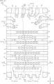
- FIG. 1 is a plan view of a semiconductor device according to a first embodiment of the present disclosure.
- FIG. 2 is a plan view corresponding to FIG. 1, seen through the semiconductor element and the sealing resin.
- FIG. 3 is a bottom view of the semiconductor device shown in FIG.
- FIG. 4 is a right side view of the semiconductor device shown in FIG.
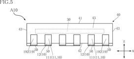
- FIG. 5 is a front view of the semiconductor device shown in FIG.
- FIG. 6 is a cross-sectional view taken along line VI-VI in FIG.
- FIG. 7 is a cross-sectional view taken along line VII-VII in FIG.
- FIG. 8 is a cross-sectional view taken along line VIII-VIII in FIG.
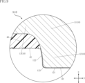
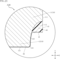
- FIG. 9 is an enlarged cross-sectional view of a portion of FIG.
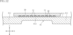
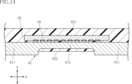
- FIG. 10A to 10C are cross-sectional views for explaining the manufacturing process of the semiconductor device shown in FIG. 11A to 11C are cross-sectional views for explaining a manufacturing process of the semiconductor device shown in FIG. 12A to 12C are cross-sectional views illustrating a manufacturing process of the semiconductor device shown in FIG. 13A to 13C are cross-sectional views for explaining a manufacturing process of the semiconductor device shown in FIG. 14A to 14C are cross-sectional views for explaining a manufacturing process of the semiconductor device shown in FIG. 15A to 15C are cross-sectional views for explaining a manufacturing process of the semiconductor device shown in FIG. 16A to 16C are cross-sectional views for explaining a manufacturing process of the semiconductor device shown in FIG. FIG.
- FIG. 17 is a plan view of the semiconductor device according to the second embodiment of the present disclosure, seen through the semiconductor element and the sealing resin.
- 18 is a bottom view of the semiconductor device shown in FIG.
- FIG. 19 is a cross-sectional view taken along line XIX-XIX in FIG.
- FIG. 20 is a cross-sectional view taken along line XX-XX in FIG. 21 is a partially enlarged cross-sectional view of FIG.
- the semiconductor device A10 includes a plurality of terminals 10, four dummy terminals 19, a plurality of bonding layers 20, a semiconductor element 30, a sealing resin 40, and a plurality of coating layers 50.
- the semiconductor device A10 is in a resin package format that is surface-mounted on a wiring board.
- the resin package format is a QFN (quad flat non-leaded package) in which a plurality of leads do not protrude from the sealing resin 40.
- FIG. 2 shows the semiconductor element 30 and the sealing resin 40 through the transparent view for ease of understanding.
- the semiconductor element 30 and the sealing resin 40 through the transparent view are each shown by an imaginary line (two-dot chain line).
- the VI-VI line is shown by a dashed line.
- the normal direction of each of the main surfaces 10A of the multiple terminals 10 described below is referred to as the "first direction z.”
- One direction perpendicular to the first direction z is referred to as the “second direction x.”
- the direction perpendicular to the first direction z and the second direction x is referred to as the "third direction y.”
- the semiconductor device A10 is rectangular when viewed in the first direction z (in a plan view).
- the sealing resin 40 covers a portion of each of the multiple terminals 10 and the semiconductor element 30.
- the sealing resin 40 has electrical insulation properties.
- One example of a material for the sealing resin 40 is black epoxy resin.
- the sealing resin 40 has a top surface 41, a bottom surface 42, and multiple side surfaces 43.
- the top surface 41 and the bottom surface 42 face opposite each other in the first direction z.
- the bottom surface 42 is disposed on the opposite side of the first direction z from the side on which the semiconductor element 30 is located, with the multiple terminals 10 as a reference.
- Each of the multiple side surfaces 43 is located between the top surface 41 and the bottom surface 42 in the first direction z.
- Each of the multiple side surfaces 43 faces in a direction perpendicular to the first direction z.
- the bottom surface 42 is rough.
- the surface roughness of the bottom surface 42 is greater than the surface roughness of the top surface 41.
- the multiple terminals 10 are equipped with a semiconductor element 30. Each of the multiple terminals 10 forms a conductive path between the semiconductor element 30 and the wiring board on which the semiconductor device A10 is mounted.
- the multiple terminals 10 contain copper (Cu).
- the multiple terminals 10 are obtained from the same lead frame.
- each of the multiple terminals 10 has at least one base 11, at least one protrusion 12, and a protruding portion 13.
- the number of protrusions 12 is equal to the number of bases 11.
- Each of the multiple terminals 10 has a main surface 10A that faces the same side as the top surface 41 of the sealing resin 40 in the first direction z.
- the main surface 10A faces the semiconductor element 30.
- Each of the bases 11 and the protruding portions 13 includes a main surface 10A.
- the base 11 is housed in the sealing resin 40.
- the base 11 has an end face 111.
- the end face 111 faces a direction perpendicular to the first direction z.
- the end face 111 is exposed to the outside from one of the multiple side faces 43 of the sealing resin 40.
- the end face 111 is flush with one of the multiple side faces 43.
- the protrusion 12 is connected to the base 11.
- the protrusion 12 protrudes outward from the bottom surface 42 of the sealing resin 40.
- the dimension of the protrusion 12 in the first direction z is smaller than the dimension of the base 11 in the first direction z.
- the protrusion 12 has a mounting surface 121 and a peripheral surface 122.
- the mounting surface 121 faces the same side as the bottom surface 42 of the sealing resin 40 in the first direction z. When viewed in the first direction z, the entire mounting surface 121 overlaps the main surface 10A of the base 11.
- the peripheral surface 122 is located between the mounting surface 121 and the end surface 111 of the base 11 in the first direction z.
- the peripheral surface 122 surrounds the mounting surface 121. When viewed in the first direction z, the entire peripheral surface 122 overlaps the main surface 10A of the base 11. In the semiconductor device A10, the peripheral surface 122 is connected to the end surface 111.
- the peripheral surface 122 is a curved surface that is concave inwardly of the terminal 10.
- the protrusion 12 has a boundary surface 123 that connects the mounting surface 121 and the peripheral surface 122.
- the boundary surface 123 is convex toward the outside of the terminal 10.
- the protrusion 13 extends from the base 11 in a direction perpendicular to the first direction z.
- the protrusion 13 is spaced apart from the bottom surface 42 of the sealing resin 40.
- the protrusion 13 is sandwiched between the sealing resin 40 in the first direction z.
- the protrusion 13 of any of the multiple terminals 10 is exposed from any of the multiple side surfaces 43 of the sealing resin 40.
- the four dummy terminals 19 are arranged at the four corners of the semiconductor device A10. Unlike the multiple terminals 10, the four dummy terminals 19 are not electrically connected to the semiconductor element 30. Each of the four dummy terminals 19 protrudes outward from the bottom surface 42 of the sealing resin 40.
- each of the four dummy terminals 19 has a first surface 191, two second surfaces 192, and a third surface 193.
- the first surface 191 faces the same side as the bottom surface 42 of the sealing resin 40 in the first direction z.
- Each of the two second surfaces 192 faces in a direction perpendicular to the first direction z.
- Each of the two second surfaces 192 is exposed to the outside from one of the multiple side surfaces 43 of the sealing resin 40.
- the third surface 193 faces in a direction perpendicular to the first direction z and is located between the two second surfaces 192.
- the third surface 193 is inclined with respect to each of the second direction x and the third direction y.
- the third surface 193 is covered by the sealing resin 40.
- each of the multiple bonding layers 20 is mounted on one of the main surfaces 10A of the multiple terminals 10. Each of the multiple bonding layers 20 is in contact with the main surface 10A.
- the multiple bonding layers 20 contain nickel (Ni), tin (Sn) and silver (Ag).
- the conductive bonding layer 29 may contain nickel, tin and antimony (Sb).
- the semiconductor element 30 is mounted on multiple terminals 10.
- the semiconductor element 30 is, for example, an LSI (Large Scale Integration).
- the semiconductor element 30 has multiple electrodes 31.
- each of the multiple electrodes 31 faces the main surface 10A of each of the multiple terminals 10.
- Each of the multiple electrodes 31 is conductively bonded to the main surface 10A of one of the multiple terminals 10 via one of the multiple bonding layers 20. This allows the semiconductor element 30 to be electrically connected to the multiple terminals 10.
- the multiple coating layers 50 are exposed to the outside as shown in Figures 3 to 8. Each of the multiple coating layers 50 covers the mounting surface 121 and peripheral surface 122 of the protrusion 12 of one of the multiple terminals 10, or the first surface 191 of one of the multiple dummy terminals 19.
- the multiple coating layers 50 are conductors.
- the multiple coating layers 50 are conductively bonded to the wiring board via solder, thereby mounting the semiconductor device A10 on the wiring board.
- Each of the multiple coating layers 50 contains a metal element.
- the metal element is either tin or gold.
- each of the multiple coating layers 50 may include multiple metal layers.
- the multiple metal layers are stacked in the order of a nickel layer and a gold (Au) layer from the side closer to the protruding portion 12 of any of the multiple terminals 10 or the first surface 191 of any of the four dummy terminals 19.
- the multiple metal layers may have a palladium (Pd) layer sandwiched between the nickel layer and the gold layer.
- a plurality of terminals 81 are formed by removing a portion of the lead frame.
- Each of the plurality of terminals 81 has a main surface 81A facing one side in the first direction z.
- the plurality of terminals 81 are formed by removing a portion of the lead frame located on the opposite side in the first direction z to the side to which the main surface 81A faces, by wet etching.
- This process forms a plurality of terminals 81 having at least one first portion 811 and a second portion 812.
- the first portion 811 corresponds to the base 11 and protruding portion 12 of the terminal 10.
- the second portion 812 corresponds to the overhanging portion 13 of the terminal 10.
- a plurality of bonding layers 20 are formed on the main surface 81A of each of the plurality of terminals 81.
- the plurality of bonding layers 20 are formed by performing photolithography patterning on the main surface 81A, and then depositing a plurality of metal layers by electrolytic plating using the plurality of terminals 81 as conductive paths.
- each of the multiple electrodes 31 of the semiconductor element 30 is conductively bonded to one of the multiple terminals 81.
- the conductive bonding of the semiconductor element 30 is performed by flip-chip bonding.
- the conductive bonding of the semiconductor element 30 is performed by temporarily attaching each of the multiple electrodes 31 individually to the multiple bonding layers 20, and then melting and solidifying the multiple bonding layers 20 by reflow.
- a sealing resin 82 is formed to cover a portion of each of the multiple terminals 81 and the semiconductor element 30.
- a portion of each of the multiple terminals 81 and the semiconductor element 30 are covered with the sealing resin 82.
- This process forms the sealing resin 82 having a top surface 821.
- the top surface 821 faces the same side as the main surface 81A of each of the multiple terminals 81 in the first direction z.
- the top surface 821 corresponds to the top surface 41 of the sealing resin 40.
- a part of the sealing resin 82 located on the opposite side of the semiconductor element 30 with respect to the multiple terminals 81 in the first direction z is removed.
- This removal forms a bottom surface 822, and the first parts 811 of the multiple terminals 81 protrude outward from the bottom surface 822 of the sealing resin 82.
- the bottom surface 822 faces the opposite side of the top surface 821 in the first direction z.
- the bottom surface 822 corresponds to the bottom surface 42 of the sealing resin 40.
- wet blasting can be used. Wet blasting is a method of performing a blasting process by mixing an abrasive (for example, silica sand) with water. By using wet blasting, the surface roughness of the bottom surface 822 becomes greater than the surface roughness of the top surface 821.
- the surface of each of the first portions 811 of the multiple terminals 81 protruding outward from the bottom surface 822 of the sealing resin 82 is smoothed by wet etching, and then multiple coating layers 50 are formed to individually cover the surfaces.
- the multiple coating layers 50 are formed by electrolytic plating using the multiple terminals 81 as conductive paths. Alternatively, the multiple coating layers 50 can be formed by electroless plating.
- the multiple terminals 81 and the sealing resin 82 are cut using a blade 89.
- the multiple terminals 81 and the sealing resin 82 are cut so as to form a lattice pattern along each of the second direction x and the third direction y.
- the multiple terminals 81 become multiple terminals 10
- the sealing resin 82 becomes the sealing resin 40.
- the semiconductor device A10 is obtained.
- the semiconductor device A10 comprises a terminal 10, a semiconductor element 30 located on one side of the terminal 10 in the first direction z and conductive to the terminal 10, and a sealing resin 40 covering a part of the terminal 10 and the semiconductor element 30.
- the sealing resin 40 has a bottom surface 42 located on the opposite side of the terminal 10 in the first direction z from the side on which the semiconductor element 30 is located.
- the terminal 10 protrudes outward from the bottom surface 42.
- the dimension of the protrusion 12 of the terminal 10 in the first direction z is smaller than the dimension of the base 11 of the terminal 10 in the first direction z.
- the protrusion 12 of the terminal 10 has a mounting surface 121 that faces the same side as the bottom surface 42 of the sealing resin 40 in the first direction z. When viewed in the first direction z, the entire mounting surface 121 overlaps the main surface 10A of the terminal 10. This configuration makes it possible to suppress the expansion of the dimensions of the terminal 10 in a direction perpendicular to the first direction z.
- the protrusion 12 of the terminal 10 has a peripheral surface 122 located between the mounting surface 121 and the end surface 111 of the base 11 of the terminal 10 in the first direction z.
- the peripheral surface 122 surrounds the mounting surface 121.
- the entire peripheral surface 122 overlaps the main surface 10A of the terminal 10.
- the peripheral surface 122 is roughly perpendicular to the mounting surface 121.
- the semiconductor device A10 further includes a coating layer 50 that covers the mounting surface 121 and the peripheral surface 122 of the protrusion 12.
- the coating layer 50 contains either the metal element tin or gold. This configuration improves the wettability of the solder to the protrusion 12 when the semiconductor device A10 is mounted on a wiring board. This makes it possible to prevent a reduction in the contact area of the protrusion 12 with the solder.
- the surface roughness of the bottom surface 42 of the sealing resin 40 is greater than the surface roughness of the top surface 41 of the sealing resin 40.
- the protrusion 12 of the terminal 10 has an interface 123 connecting the mounting surface 121 and the peripheral surface 122.
- the interface 123 is convex toward the outside of the terminal 10.
- the semiconductor device A10 further includes four dummy terminals 19 arranged at the four corners of the semiconductor device A10 when viewed in the first direction z.
- the four dummy terminals 19 are not electrically connected to the semiconductor element 30. This configuration allows the thermal stress caused by the heat generated by the semiconductor device A10 to be concentrated on the four dummy terminals 19. This reduces the occurrence of cracks in the solder joining the wiring board and the terminals 10.
- FIG. 17 shows the semiconductor element 30 and the sealing resin 40 through a see-through view.
- the see-through semiconductor element 30 and the sealing resin 40 are each shown by imaginary lines.
- line XIX-XIX is shown by a dashed line.
- semiconductor device A20 the configuration of the multiple terminals 10 is different from that of semiconductor device A10.
- each of the bases 11 of the multiple terminals 10 is spaced apart from the bottom surface 42 of the sealing resin 40.
- the base 11 of each of the multiple terminals 10 has an intermediate surface 112.
- the intermediate surface 112 is connected to the end surface 111 of the base 11 and the peripheral surface 122 of one of the protrusions 12 of the multiple terminals 10.
- the entire intermediate surface 112 overlaps the main surface 10A of the base 11.
- the intermediate surface 112 is a curved surface that is recessed inward of the terminal 10.
- the intermediate surface 112 is covered with sealing resin 40.
- the semiconductor device A20 comprises a terminal 10, a semiconductor element 30 located on one side of the terminal 10 in the first direction z and conductive to the terminal 10, and a sealing resin 40 covering a part of the terminal 10 and the semiconductor element 30.
- the sealing resin 40 has a bottom surface 42 located on the opposite side of the terminal 10 in the first direction z from the side on which the semiconductor element 30 is located.
- the terminal 10 protrudes outward from the bottom surface 42. Therefore, with this configuration, it is possible to improve the bonding strength of the semiconductor device A20 to the wiring board in the semiconductor device A20 as well. Furthermore, by being provided with a configuration in common with the semiconductor device A10, the semiconductor device A20 achieves the same effects as the semiconductor device A10.
- the mounting surface 121 of the protrusion 12 of the terminal 10 is spaced from the bottom surface 42 of the sealing resin 40. This configuration restricts the solder from creeping up the end surface 111 of the base 11 of the terminal 10 exposed to the outside from the sealing resin 40 when the semiconductor device A20 is mounted on a wiring board. This reduces the erosion of the terminal 10 by the solder.
- the base 11 of the terminal 10 has an intermediate surface 112 that connects the end surface 111 of the base 11 and the peripheral surface 122 of the protrusion 12.
- the intermediate surface 112 is recessed inward of the terminal 10 and is covered with sealing resin 40.
- Appendix 1 The terminals and a semiconductor element located on one side of the terminal in a first direction and electrically connected to the terminal; a sealing resin that covers a portion of the terminal and the semiconductor element, the sealing resin has a bottom surface that is disposed on an opposite side to a side on which the semiconductor element is located with respect to the terminal in the first direction, The terminal protrudes outward from the bottom surface.
- Appendix 2. The terminal has a base and a protrusion connected to the base, the base portion is accommodated in the sealing resin, The protrusion protrudes outward from the bottom surface, 2.
- Appendix 3. The semiconductor device according to claim 2, wherein the end surface is exposed to the outside from the sealing resin.
- Appendix 4. 4. The semiconductor device according to claim 3, wherein a dimension of the protrusion in the first direction is smaller than a dimension of the base in the first direction.
- Appendix 5. the sealing resin has a top surface facing a side opposite to the bottom surface in the first direction, 5.
- Appendix 6. the terminal has a main surface facing the same side as the top surface in the first direction, the protrusion has a mounting surface facing the same side as the bottom surface in the first direction, 6.
- the mounting surface is entirely overlapped with the main surface.
- Appendix 7. the protrusion has a peripheral surface located between the mounting surface and the end surface in the first direction, 7.
- the semiconductor device according to claim 6, wherein, when viewed in the first direction, the entire peripheral surface overlaps the main surface.
- Appendix 8. The semiconductor device according to claim 7, wherein the peripheral surface is recessed inwardly of the terminal.
- Appendix 9. the protrusion has a boundary surface connecting the mounting surface and the peripheral surface, 9. The semiconductor device according to claim 8, wherein the boundary surface is convex toward an outside of the terminal. Appendix 10. 8.
- the semiconductor device wherein, when viewed in the first direction, the mounting surface is spaced apart from a peripheral edge of the bottom surface.
- Appendix 11. The semiconductor device of claim 10, wherein the end surface is spaced from the bottom surface.
- Appendix 12. The base portion has an intermediate surface that is connected to the end surface and the peripheral surface, 12. The semiconductor device according to claim 11, wherein the intermediate surface is recessed toward the inside of the terminal and is covered with the sealing resin.
- Appendix 13 has a protruding portion extending from the base portion in a direction perpendicular to the first direction, and each of the base portion and the protruding portion includes the main surface. 13. The semiconductor device according to claim 7, wherein the protruding portion is spaced apart from the bottom surface. Appendix 14.
- the semiconductor element has an electrode facing the main surface, 14.
- Appendix 15. a coating layer covering the mounting surface and the peripheral surface, The semiconductor device according to claim 14, wherein the coating layer contains a metal element.
- Appendix 16. The semiconductor device according to claim 15, wherein the metal element includes either tin or gold. Appendix 17.
- a terminal a step of conductively joining a semiconductor element to one side of the terminal in a first direction; forming a sealing resin to cover the semiconductor element;
- a method for manufacturing a semiconductor device in which, in the process of forming the sealing resin, after covering the semiconductor element with the sealing resin, a portion of the sealing resin that is located on the opposite side of the semiconductor element from the terminal is removed so that a portion of the terminal protrudes outward from the sealing resin.
- Appendix 18. 18 The method for manufacturing a semiconductor device according to claim 17, wherein in the step of forming the terminal, the terminal is formed by removing a part of a lead frame by etching.
Landscapes
- Structures Or Materials For Encapsulating Or Coating Semiconductor Devices Or Solid State Devices (AREA)
- Engineering & Computer Science (AREA)
- Microelectronics & Electronic Packaging (AREA)
- Physics & Mathematics (AREA)
- Geometry (AREA)
Priority Applications (2)
| Application Number | Priority Date | Filing Date | Title |
|---|---|---|---|
| JP2025510170A JPWO2024203110A1 (https=) | 2023-03-24 | 2024-03-07 | |
| US19/331,684 US20260018495A1 (en) | 2023-03-24 | 2025-09-17 | Semiconductor device and manufacturing method for semiconductor device |
Applications Claiming Priority (2)
| Application Number | Priority Date | Filing Date | Title |
|---|---|---|---|
| JP2023-047967 | 2023-03-24 | ||
| JP2023047967 | 2023-03-24 |
Related Child Applications (1)
| Application Number | Title | Priority Date | Filing Date |
|---|---|---|---|
| US19/331,684 Continuation US20260018495A1 (en) | 2023-03-24 | 2025-09-17 | Semiconductor device and manufacturing method for semiconductor device |
Publications (1)
| Publication Number | Publication Date |
|---|---|
| WO2024203110A1 true WO2024203110A1 (ja) | 2024-10-03 |
Family
ID=92905611
Family Applications (1)
| Application Number | Title | Priority Date | Filing Date |
|---|---|---|---|
| PCT/JP2024/008720 Ceased WO2024203110A1 (ja) | 2023-03-24 | 2024-03-07 | 半導体装置、および半導体装置の製造方法 |
Country Status (3)
| Country | Link |
|---|---|
| US (1) | US20260018495A1 (https=) |
| JP (1) | JPWO2024203110A1 (https=) |
| WO (1) | WO2024203110A1 (https=) |
Citations (7)
| Publication number | Priority date | Publication date | Assignee | Title |
|---|---|---|---|---|
| US5866939A (en) * | 1996-01-21 | 1999-02-02 | Anam Semiconductor Inc. | Lead end grid array semiconductor package |
| JP2008112961A (ja) * | 2006-10-04 | 2008-05-15 | Rohm Co Ltd | 半導体装置の製造方法および半導体装置 |
| US20100224970A1 (en) * | 2009-03-09 | 2010-09-09 | Asat Ltd. | Leadless integrated circuit package having standoff contacts and die attach pad |
| JP2017028200A (ja) * | 2015-07-27 | 2017-02-02 | 新光電気工業株式会社 | 半導体装置及び半導体装置の製造方法 |
| JP2017130576A (ja) * | 2016-01-21 | 2017-07-27 | Shマテリアル株式会社 | リードフレーム及びこれを用いた半導体装置、並びにそれらの製造方法 |
| JP2019050302A (ja) * | 2017-09-11 | 2019-03-28 | ローム株式会社 | 半導体装置 |
| JP2022143657A (ja) * | 2021-03-18 | 2022-10-03 | 株式会社東芝 | 半導体装置及びその製造方法 |
-
2024
- 2024-03-07 WO PCT/JP2024/008720 patent/WO2024203110A1/ja not_active Ceased
- 2024-03-07 JP JP2025510170A patent/JPWO2024203110A1/ja active Pending
-
2025
- 2025-09-17 US US19/331,684 patent/US20260018495A1/en active Pending
Patent Citations (7)
| Publication number | Priority date | Publication date | Assignee | Title |
|---|---|---|---|---|
| US5866939A (en) * | 1996-01-21 | 1999-02-02 | Anam Semiconductor Inc. | Lead end grid array semiconductor package |
| JP2008112961A (ja) * | 2006-10-04 | 2008-05-15 | Rohm Co Ltd | 半導体装置の製造方法および半導体装置 |
| US20100224970A1 (en) * | 2009-03-09 | 2010-09-09 | Asat Ltd. | Leadless integrated circuit package having standoff contacts and die attach pad |
| JP2017028200A (ja) * | 2015-07-27 | 2017-02-02 | 新光電気工業株式会社 | 半導体装置及び半導体装置の製造方法 |
| JP2017130576A (ja) * | 2016-01-21 | 2017-07-27 | Shマテリアル株式会社 | リードフレーム及びこれを用いた半導体装置、並びにそれらの製造方法 |
| JP2019050302A (ja) * | 2017-09-11 | 2019-03-28 | ローム株式会社 | 半導体装置 |
| JP2022143657A (ja) * | 2021-03-18 | 2022-10-03 | 株式会社東芝 | 半導体装置及びその製造方法 |
Also Published As
| Publication number | Publication date |
|---|---|
| JPWO2024203110A1 (https=) | 2024-10-03 |
| US20260018495A1 (en) | 2026-01-15 |
Similar Documents
| Publication | Publication Date | Title |
|---|---|---|
| TW398063B (en) | Lead frame and its manufacturing method thereof | |
| US20110201159A1 (en) | Semiconductor package and manufacturing method thereof | |
| JP7089388B2 (ja) | 半導体装置および半導体装置の製造方法 | |
| JP4032063B2 (ja) | 半導体装置の製造方法 | |
| WO2007018237A1 (ja) | 半導体装置及びその製造方法 | |
| JP5151158B2 (ja) | パッケージ、およびそのパッケージを用いた半導体装置 | |
| KR100611291B1 (ko) | 회로 장치, 회로 모듈 및 회로 장치의 제조 방법 | |
| US20050189627A1 (en) | Method of surface mounting a semiconductor device | |
| JP7193284B2 (ja) | リードフレーム及びリードフレームの製造方法 | |
| JPWO2020166512A1 (ja) | 半導体装置、および、半導体装置の製造方法 | |
| TW201705426A (zh) | 樹脂密封型半導體裝置及其製造方法 | |
| JP2006294701A (ja) | 半導体装置及びその製造方法 | |
| WO2024203110A1 (ja) | 半導体装置、および半導体装置の製造方法 | |
| JP7550932B2 (ja) | 半導体装置 | |
| JP2010016395A (ja) | 半導体装置の製造方法 | |
| JP2006147918A (ja) | 半導体装置 | |
| US20250372485A1 (en) | Semiconductor device | |
| JP2007048978A (ja) | 半導体装置及びその製造方法 | |
| JP2024128422A (ja) | 半導体装置 | |
| JP7154818B2 (ja) | 半導体装置および半導体装置の製造方法 | |
| US20250300101A1 (en) | Electronic device | |
| JP2017188604A (ja) | リードフレーム及び半導体装置、並びにそれらの製造方法 | |
| JPH1070211A (ja) | テープキャリア及びその製造方法 | |
| US20250379126A1 (en) | Semiconductor device and method of manufacturing semiconductor device | |
| JP7254602B2 (ja) | 半導体装置、および半導体装置の製造方法 |
Legal Events
| Date | Code | Title | Description |
|---|---|---|---|
| 121 | Ep: the epo has been informed by wipo that ep was designated in this application |
Ref document number: 24779244 Country of ref document: EP Kind code of ref document: A1 |
|
| ENP | Entry into the national phase |
Ref document number: 2025510170 Country of ref document: JP Kind code of ref document: A |
|
| WWE | Wipo information: entry into national phase |
Ref document number: 2025510170 Country of ref document: JP |
|
| NENP | Non-entry into the national phase |
Ref country code: DE |
|
| 122 | Ep: pct application non-entry in european phase |
Ref document number: 24779244 Country of ref document: EP Kind code of ref document: A1 |