WO2024202710A1 - 積層セラミック電子部品 - Google Patents
積層セラミック電子部品 Download PDFInfo
- Publication number
- WO2024202710A1 WO2024202710A1 PCT/JP2024/006012 JP2024006012W WO2024202710A1 WO 2024202710 A1 WO2024202710 A1 WO 2024202710A1 JP 2024006012 W JP2024006012 W JP 2024006012W WO 2024202710 A1 WO2024202710 A1 WO 2024202710A1
- Authority
- WO
- WIPO (PCT)
- Prior art keywords
- electrode
- electronic component
- ceramic electronic
- multilayer ceramic
- extreme value
- Prior art date
- Legal status (The legal status is an assumption and is not a legal conclusion. Google has not performed a legal analysis and makes no representation as to the accuracy of the status listed.)
- Ceased
Links
Images





Classifications
-
- H—ELECTRICITY
- H01—ELECTRIC ELEMENTS
- H01G—CAPACITORS; CAPACITORS, RECTIFIERS, DETECTORS, SWITCHING DEVICES, LIGHT-SENSITIVE OR TEMPERATURE-SENSITIVE DEVICES OF THE ELECTROLYTIC TYPE
- H01G4/00—Fixed capacitors; Processes of their manufacture
- H01G4/002—Details
- H01G4/018—Dielectrics
- H01G4/06—Solid dielectrics
- H01G4/08—Inorganic dielectrics
- H01G4/12—Ceramic dielectrics
-
- H—ELECTRICITY
- H01—ELECTRIC ELEMENTS
- H01C—RESISTORS
- H01C7/00—Non-adjustable resistors formed as one or more layers or coatings; Non-adjustable resistors made from powdered conducting material or powdered semi-conducting material with or without insulating material
- H01C7/02—Non-adjustable resistors formed as one or more layers or coatings; Non-adjustable resistors made from powdered conducting material or powdered semi-conducting material with or without insulating material having positive temperature coefficient
-
- H—ELECTRICITY
- H01—ELECTRIC ELEMENTS
- H01C—RESISTORS
- H01C7/00—Non-adjustable resistors formed as one or more layers or coatings; Non-adjustable resistors made from powdered conducting material or powdered semi-conducting material with or without insulating material
- H01C7/04—Non-adjustable resistors formed as one or more layers or coatings; Non-adjustable resistors made from powdered conducting material or powdered semi-conducting material with or without insulating material having negative temperature coefficient
-
- H—ELECTRICITY
- H01—ELECTRIC ELEMENTS
- H01C—RESISTORS
- H01C7/00—Non-adjustable resistors formed as one or more layers or coatings; Non-adjustable resistors made from powdered conducting material or powdered semi-conducting material with or without insulating material
- H01C7/10—Non-adjustable resistors formed as one or more layers or coatings; Non-adjustable resistors made from powdered conducting material or powdered semi-conducting material with or without insulating material voltage responsive, i.e. varistors
-
- H—ELECTRICITY
- H01—ELECTRIC ELEMENTS
- H01F—MAGNETS; INDUCTANCES; TRANSFORMERS; SELECTION OF MATERIALS FOR THEIR MAGNETIC PROPERTIES
- H01F27/00—Details of transformers or inductances, in general
- H01F27/28—Coils; Windings; Conductive connections
- H01F27/29—Terminals; Tapping arrangements for signal inductances
-
- H—ELECTRICITY
- H01—ELECTRIC ELEMENTS
- H01G—CAPACITORS; CAPACITORS, RECTIFIERS, DETECTORS, SWITCHING DEVICES, LIGHT-SENSITIVE OR TEMPERATURE-SENSITIVE DEVICES OF THE ELECTROLYTIC TYPE
- H01G4/00—Fixed capacitors; Processes of their manufacture
- H01G4/002—Details
- H01G4/005—Electrodes
- H01G4/012—Form of non-self-supporting electrodes
-
- H—ELECTRICITY
- H01—ELECTRIC ELEMENTS
- H01G—CAPACITORS; CAPACITORS, RECTIFIERS, DETECTORS, SWITCHING DEVICES, LIGHT-SENSITIVE OR TEMPERATURE-SENSITIVE DEVICES OF THE ELECTROLYTIC TYPE
- H01G4/00—Fixed capacitors; Processes of their manufacture
- H01G4/002—Details
- H01G4/228—Terminals
- H01G4/232—Terminals electrically connecting two or more layers of a stacked or rolled capacitor
-
- H—ELECTRICITY
- H01—ELECTRIC ELEMENTS
- H01G—CAPACITORS; CAPACITORS, RECTIFIERS, DETECTORS, SWITCHING DEVICES, LIGHT-SENSITIVE OR TEMPERATURE-SENSITIVE DEVICES OF THE ELECTROLYTIC TYPE
- H01G4/00—Fixed capacitors; Processes of their manufacture
- H01G4/002—Details
- H01G4/228—Terminals
- H01G4/248—Terminals the terminals embracing or surrounding the capacitive element, e.g. caps
-
- H—ELECTRICITY
- H01—ELECTRIC ELEMENTS
- H01G—CAPACITORS; CAPACITORS, RECTIFIERS, DETECTORS, SWITCHING DEVICES, LIGHT-SENSITIVE OR TEMPERATURE-SENSITIVE DEVICES OF THE ELECTROLYTIC TYPE
- H01G4/00—Fixed capacitors; Processes of their manufacture
- H01G4/30—Stacked capacitors
Definitions
- the present invention relates to multilayer ceramic electronic components.
- Patent Document 1 JP 2006-005105 A discloses a multilayer electronic component intended to suppress deformation of the laminate.
- this multilayer electronic component at least one of a hole and a notch is formed in the second internal electrode at a position that is closer to the second end face than the midpoint between the first end face and the second end face when viewed from a direction perpendicular to the lamination direction.
- Patent Document 2 JP 2019-009414 A discloses a laminated piezoelectric element having a laminated piezoelectric body and multiple internal electrodes.
- the laminated piezoelectric body has a pair of main surfaces facing in a first axial direction, a pair of end faces facing in a second axial direction that is perpendicular to the first axial direction and is the longitudinal direction, and a pair of side surfaces facing in a third axial direction that is perpendicular to the first axial direction and the second axial direction.
- the multiple internal electrodes are disposed inside the laminated piezoelectric body and are laminated in the first axial direction.
- a first cross section of a central internal electrode disposed in the center of the laminated piezoelectric body, as viewed from the third axial direction, has greater undulations than a second cross section of the central internal electrode as viewed from the second axial direction.
- the laminated piezoelectric element (ceramic piezoelectric component) of JP 2019-009414 A is intended to improve the displacement performance along the longitudinal direction.
- laminated ceramic electronic components in general not limited to ceramic piezoelectric components, there is often a demand for improved electrical characteristics while being constrained by the upper limit of the size of the laminated ceramic electronic components.
- An example of improved electrical characteristics is improved capacitance.
- the present invention was made to solve the above problems, and its purpose is to provide a multilayer ceramic electronic component that has improved electrical characteristics without significantly affecting insulation reliability while being subject to upper size restrictions.
- Aspect 1 is a multilayer ceramic electronic component having a thickness direction, a width direction perpendicular to the thickness direction, and a length direction perpendicular to the thickness direction and the width direction, and includes a ceramic part having a first surface and a second surface opposite to each other in the thickness direction, a first electrode having a first portion disposed on the first surface, and a second electrode having a second portion disposed on the second surface, and each of the first surface and the second surface of the ceramic part has a width dimension in the width direction, a length dimension in the length direction that is greater than the width dimension and is 1 mm or less, and a surface profile along the length direction that includes a warp of 2 ⁇ m or more in the thickness direction.
- Aspect 2 is a multilayer ceramic electronic component according to aspect 1, in which the ceramic part has a third surface and a fourth surface opposite each other in the longitudinal direction, the first electrode has a third portion disposed on the third surface, and the second electrode has a fourth portion disposed on the fourth surface.
- Aspect 3 is a multilayer ceramic electronic component according to aspect 2, in which the first electrode has a first internal electrode layer disposed within the ceramic portion and connected to the third portion.
- Aspect 4 is a multilayer ceramic electronic component according to aspect 3, in which the second electrode has a second internal electrode layer disposed within the ceramic portion and connected to the fourth portion.
- Aspect 5 is a multilayer ceramic electronic component according to any one of aspects 1 to 4, in which the surface profile has multiple extreme values.
- Aspect 6 is a multilayer ceramic electronic component according to aspect 5, in which at least one of the first surface and the second surface has a slit region sandwiched between a region covered by the first electrode and a region covered by the second electrode, and any one of the multiple extreme values of each of the first surface and the second surface is present in the slit region of the first surface or the second surface.
- Aspect 7 is a multilayer ceramic electronic component according to aspect 5 or 6, in which the multiple extreme values are two extreme values, a first extreme value and a second extreme value.
- Aspect 8 is a multilayer ceramic electronic component according to aspect 7, in which the first extreme value and the second extreme value are located at a first position and a second position, respectively, in the longitudinal direction, and the distance from the midpoint of the surface profile to the second position is greater than the distance from the midpoint to the first position in the longitudinal direction.
- Aspect 9 is a multilayer ceramic electronic component according to aspect 8, in which the absolute value of the second extreme value is smaller than the absolute value of the first extreme value under leveling such that the values at both ends of the surface profile are zero.
- Aspect 10 is a multilayer ceramic electronic component according to any one of aspects 7 to 9, in which the absolute value of the second extreme value is 0.2 ⁇ m or more and less than half the absolute value of the first extreme value.
- the above aspect makes it possible to improve electrical characteristics without significantly affecting insulation reliability while still being subject to upper size restrictions.
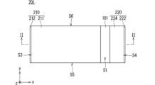
- FIG. 1 is a top view illustrating a schematic configuration of a multilayer ceramic electronic component according to a first embodiment.
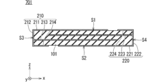
- 2 is a schematic cross-sectional view taken along line II-II in FIG. 1.
- 2 is a diagram showing a schematic surface profile of a ceramic part of the multilayer ceramic electronic component according to the first embodiment;
- FIG. 4 is a graph showing an example of the measurement results of the surface profile corresponding to FIG. 3 .
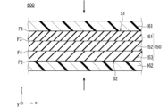
- 3 is a partial cross-sectional view illustrating a first step of a method for manufacturing the multilayer ceramic electronic component according to the first embodiment.
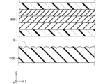
- FIG. 4 is a partial cross-sectional view illustrating a second step of the method for manufacturing the multilayer ceramic electronic component according to the first embodiment.
- FIG. 11 is a diagram showing a schematic surface profile of a ceramic part of a multilayer ceramic electronic component according to a second embodiment.
- FIG. FIG. 8 is a graph showing an example of the measurement results of the surface profile corresponding to FIG. 7 .
- 11 is a cross-sectional view illustrating a schematic configuration of a multilayer ceramic electronic component according to a third embodiment of the present invention.
- FIG. 11 is a cross-sectional view illustrating a schematic configuration of a multilayer ceramic electronic component according to a fourth embodiment of the present invention.
- Fig. 1 is a top view that shows a schematic configuration of a multilayer ceramic electronic component 701 according to the present embodiment.
- Fig. 2 is a schematic cross-sectional view taken along line II-II in Fig. 1.
- the multilayer ceramic electronic component 701 has a thickness direction (z direction), a width direction (y direction) perpendicular to the thickness direction, and a length direction (x direction) perpendicular to the thickness direction and the width direction.
- the multilayer ceramic electronic component 701 has a ceramic part 101, a first electrode 210, and a second electrode 220.
- the multilayer ceramic electronic component 701 may be a chip-shaped electronic component, such as a chip capacitor.
- the ceramic part 101 may be made of an insulator.
- the ceramic part 101 has a first surface S1 and a second surface S2 that are opposite to each other in the thickness direction.
- the first surface S1 and the second surface S2 are approximately parallel to each other.
- the ceramic part 101 may also have a third surface S3 and a fourth surface S4 that are opposite to each other in the length direction.
- the third surface S3 and the fourth surface S4 may be approximately parallel to each other.
- the ceramic part 101 may also have a fifth surface S5 and a sixth surface S6 that are opposite to each other in the width direction.
- the fifth surface S5 and the sixth surface S6 may be approximately parallel to each other.
- the ceramic part 101 has a length dimension (dimension in the x direction), a width dimension (dimension in the y direction), and a thickness dimension (dimension in the z direction).
- the length dimension is greater than each of the width dimension and the thickness dimension.
- the width dimension may be greater than the thickness dimension.
- the length dimension may be 0.5 mm or more and 1 mm or less.
- the width dimension may be 0.1 mm or more and 0.3 mm or less.
- the thickness dimension may be 0.03 mm or more and 0.07 mm or less.
- the first electrode 210 includes a portion 211 (first portion) disposed on the first surface S1.
- the first electrode 210 may further include a portion 212 (third portion) disposed on the third surface S3.
- the first electrode 210 may also have a portion 214 disposed on the second surface S2.
- the first electrode 210 may also have a first internal electrode layer 213 disposed in the ceramic portion 101, and the first internal electrode layer 213 may be connected to the portion 212.
- the first electrode 210 is, for example, a platinum (Pt) electrode.
- the second electrode 220 includes a portion 221 (second portion) arranged on the second surface S2. Furthermore, the second electrode 220 may include a portion 222 (fourth portion) arranged on the fourth surface S4. The second electrode 220 may also have a portion 224 arranged on the first surface S1. The second electrode 220 may also have a second internal electrode layer 223 arranged in the ceramic part 101, and the second internal electrode layer 223 may be connected to the portion 222.
- the second electrode 220 is, for example, a Pt electrode.
- the second electrode 220 includes a portion that faces the first electrode 210 via the ceramic portion 101 in the thickness direction. This forms a capacitance between the first electrode 210 and the second electrode 220.
- At least one of the first surface S1 and the second surface S2 may have a slit region sandwiched between an area covered by the first electrode 210 and an area covered by the second electrode 220.
- the slit region is not covered by either electrode.
- each of the first surface S1 and the second surface S2 has a slit region.
- Each of the first surface S1 and the second surface S2 of the ceramic portion has a width dimension in the width direction (y direction), a length dimension in the length direction (x direction), and a thickness dimension in the thickness direction (z direction).
- the length dimension is greater than both the width dimension and the thickness dimension.
- the length dimension may be 0.5 mm or more and 1 mm or less.
- FIG. 3 is a diagram showing a schematic view of the surface profile along the length direction (x direction) of each of the first surface S1 and the second surface S2 of the ceramic part 101 of the multilayer ceramic electronic component 701 in the first embodiment.
- the first surface S1 has a surface profile H 1 (x).
- a positive height represents that the surface protrudes, and a negative height represents that the surface is recessed.
- the second surface S2 has a surface profile H 2 (x).
- a positive height represents that the surface protrudes, and a negative height represents that the surface is recessed.
- the extreme value H 1M is a maximum value, and the extreme value H 2M is a minimum value.
- the extreme value H 1M may be a minimum value, and the extreme value H 2M may be a maximum value.
- each of the surface profile H 1 (x) of the first surface S1 and the surface profile H 2 (x) of the second surface S2 has only one extreme value.
- the absolute value of the extreme value H 1M and the absolute value of the extreme value H 2M are approximately the same value, and are within 10% of their average value, for example.
- the positions x 1 and x 2 are approximately the same value, and are within 10% of their average value, for example.
- the surface profile H 1 (x) and the surface profile H 2 (x) approximately correspond to functions with their positive and negative inversions.
- Each of the extreme values H 1M and H 2M is 2 ⁇ m or more.
- the extreme values H 1M and H 2M are regarded as the warpage of the surface profile H 1 (x) and the surface profile H 2 (x), respectively. Therefore, the magnitude of the warpage is 2 ⁇ m or more.
- the magnitude of the warpage may be 10 ⁇ m or less from the viewpoint of making the multilayer ceramic electronic component 701 suitable for surface mounting.
- FIG. 4 is a graph showing an example of the measurement result of the surface profile H 1 (x) (see FIG. 3). An example of the measurement method will be described below. The measurement method of the surface profile H 2 (x) (see FIG. 3) is similar to this.
- a surface profile measurement is performed by a laser scanner on the surface of the multilayer ceramic electronic component 701 corresponding to the first surface S1 (FIG. 2), specifically, the surface shown in FIG. 1.
- a smoothed surface profile is calculated by using the height information of 20 points before and after.
- the section of the surface profile corresponding to the non-electrode region is replaced with a surface profile complemented by a polynomial approximation based on the section corresponding to the electrode region.
- FIGS. 5 and 6 are partial cross-sectional views each showing a schematic first and second steps of the manufacturing method for the multilayer ceramic electronic component 701 (FIG. 2).
- work-in-progress 600 is formed.
- Work-in-progress 600 has substrates 161 and 162 and green laminate 150.
- Green laminate 150 is held between substrate 161 and substrate 162.
- Substrates 161 and 162 are, for example, polyethylene terephthalate (PET) films.
- Green laminate 150 has green sheets 151 to 153 stacked in the thickness direction.
- the interface F1 between the substrate 161 and the green sheet 151 corresponds to the first surface S1 when the multilayer ceramic electronic component 701 (FIG. 2) is obtained from the green laminate 150.
- the substrate 161 may be a substrate to which a slurry is applied for forming the green sheet 151.
- the interface F2 between the substrate 162 and the green sheet 153 corresponds to the second surface S2 when the multilayer ceramic electronic component 701 (FIG. 2) is obtained from the green laminate 150.
- the substrate 162 may be a substrate to which a slurry is applied for forming the green sheet 153.
- An electrode paste layer (not shown) that will become the second internal electrode layer 223 (FIG. 2) by firing is formed at the interface F3 between the green sheets 151 and 152.
- An electrode paste layer (not shown) that will become the first internal electrode layer 213 (FIG. 2) by firing is formed at the interface F4 between the green sheets 152 and 153.
- An electrode paste layer (not shown) that will become the part 211 of the first electrode 210 and the part 224 of the second electrode 220 by firing may be formed at the interface F1. Note that a part or all of this electrode paste layer may be applied after the base material 161 is removed.
- An electrode paste layer (not shown) that will become the part 214 of the first electrode 210 and the part 221 of the second electrode 220 by firing may be formed at the interface F2. Note that a part or all of this electrode paste layer may be applied after the base material 162 is removed.
- the green sheets 151 to 153 are attached to each other as a result of the lamination press process as indicated by the arrows in the figure.
- the green sheets 151 to 153 form the green laminate 150.
- the lamination press process may be performed, for example, by applying pressure as indicated by the arrows in FIG. 5 to a pair of dies (not shown) that sandwich the work-in-progress 600.
- the lamination press process may be performed while being heated.
- the conditions for the lamination press process are, for example, a load of 100 kN, a temperature of 80 degrees, and a holding time of 60 seconds.
- an additional pressing process is performed. Specifically, the work-in-progress 600 is placed between a pair of dies along its stacking direction (the vertical direction in the figure). An elastic member 1100 is inserted between the work-in-progress 600 and one of the dies. Then, the work-in-progress 600 is pressed between the pair of dies.
- the elastic member 1100 has a surface S8 facing the workpiece 600.
- the surface S8 may have a non-flat shape, and this non-flat shape may correspond to the surface profile H 1 (x).
- H 1 (x) In a typical mass production process, a large number of unfired bodies that will become a large number of multilayer ceramic electronic components 701 by firing are cut out from one workpiece 600.
- the surface S8 may be a wavy surface including a large number of convex shapes with a period corresponding to each extreme value H 1M of the large number of multilayer ceramic electronic components 701.
- the period of the waveform of the wavy surface in the x direction is equal to or less than the length dimension (dimension in the x direction) of the ceramic part 101 before firing.
- the amplitude of the waveform is appropriately set according to the magnitude of the warp to be imparted.
- the elastic member 1100 is made of, for example, silicone rubber having a thickness of 8 mm and a rubber hardness of 16.
- the rubber hardness may be a value measured using a JIS K 6249 Type A durometer.
- the additional pressing process may be performed while being heated.
- the conditions for the additional pressing process are, for example, a load of 100 kN, a temperature of 60 degrees, and a holding time of 60 seconds.
- the temperature in the additional pressing process may be higher than room temperature and lower than the temperature in the aforementioned lamination pressing process.
- the values of the load, temperature, and holding time may be increased or decreased, for example, within a range of about 20% from the values stated in the above conditions.
- the additional pressing process may be repeated multiple times.
- the relative positions of the workpiece 600 and the elastic member 1100 may be the same or different. According to the latter method, a more complicated surface profile H 1 (x) can be obtained without complicating the surface S8 of the elastic member 1100.
- green bodies are cut out from the green laminate 150, which will become the multilayer ceramic electronic component 701 when fired.
- mass production processes typically, a large number of green bodies are cut out from one green laminate 150.
- the green bodies are fired to obtain the multilayer ceramic electronic component 701.
- an additional application of an electrode paste layer may be performed at an appropriate time. If this application is performed after the above firing, additional firing is performed for the electrode paste layer.
- the ceramic part 101 has a significant warp. This increases the effective length of the first electrode 210 and the second electrode 220 (FIG. 2). Therefore, it is possible to improve electrical characteristics, such as capacitance, without significantly affecting insulation reliability while being constrained by an upper size limit.
- FIG. 7 is a diagram showing a schematic view of the surface profile along the length direction (x direction) of each of the first surface S1 and the second surface S2 of the ceramic part 102 in this embodiment.
- FIG. 8 is a graph showing an example of the measurement result of the surface profile of the first surface S1.
- the ceramic part 102 (FIG. 7) is used instead of the ceramic part 101 (FIG. 3).
- the other configurations of this embodiment are similar to those of the multilayer ceramic electronic component 701 (FIG. 2: embodiment 1), so the description thereof will not be repeated.
- the definition of the surface profile and the measurement method thereof are also similar to those of FIG. 3 (embodiment 1), so the description thereof will be omitted.
- the surface profile H 1 (x) of the first surface S1 and the surface profile H 2 (x) of the second surface S2 each have a plurality of extreme values.
- the first extreme value H 1A and the second extreme value H 1B are located at positions x 1A (first position) and x 1B (second position) in the x direction, respectively.
- the first extreme value H 2A and the second extreme value H 2B in the x direction are located at positions x 2A (first position) and x 2B (second position), respectively.
- any one of the multiple extreme values of each of the first surface S1 and the second surface S2 may be present in the slit region of the first surface S1 or the second surface S2.
- the position of any one of the multiple extreme values of each of the first surface S1 and the second surface S2 may be included within the range of the slit region of the first surface S1 or the second surface S2.
- each of the position x 1B of the first surface S1 and the position x 2B of the second surface S2 may be included within the range of the slit region of the second surface S2 (the region sandwiched between the region covered by the first electrode 210 and the region covered by the second electrode 220 of the second surface S2 with reference to FIG. 2).
- the first extreme value H 1A is a maximum value
- the first extreme value H 2A is a minimum value
- the second extreme value H 1B is a minimum value
- the second extreme value H 2B is a maximum value.
- the absolute value of the first extreme value H 1A and the absolute value of the first extreme value H 2A are approximately the same value, and are within, for example, 10% of their average value.
- the absolute value of the second extreme value H 1B and the absolute value of the second extreme value H 2B are approximately the same value, and are within, for example, 10% of their average value.
- the positions x 1A and x 2A are approximately the same value, and are within, for example, 10% of their average value.
- the positions x 1B and x 2B are approximately the same value, and are within, for example, 10% of their average value.
- the surface profile H 1 (x) and the surface profile H 2 (x) approximately correspond to functions with inverted positive and negative signs.
- the first extreme value H 1A may be a minimum value
- the first extreme value H 2A may be a maximum value
- the second extreme value H 1B may be a maximum value
- the second extreme value H 2B may be a minimum value.
- the first extreme value H 1A is the extreme value having the maximum absolute value in the surface profile H 1 (x)
- the first extreme value H 2A is the extreme value having the maximum absolute value in the surface profile H 2 (x).
- the absolute values of the first extreme value H 1A and the first extreme value H 2A are 2 ⁇ m or more.
- the absolute values of the other extreme values are 0.2 ⁇ m or more, and therefore the absolute values of the second extreme value H 1B and the second extreme value H 2B are 0.2 ⁇ m or more. From the viewpoint of making the multilayer ceramic electronic component 702 suitable for surface mounting, the absolute values of the first extreme value H 1A and the first extreme value H 2A may be 10 ⁇ m or less.
- the absolute value of the second extremum H 1B may be less than or equal to half the absolute value of the first extremum H 1A
- the absolute value of the second extremum H 2B may be less than or equal to half the absolute value of the first extremum H 2A
- Each of the surface profiles H 1 (x) of the first surface S1 and H 2 (x) of the second surface S2 may have only two extremums, in other words the first and second extremums, as shown in FIG. 7. If a further extremum is added as a variant, the absolute value of this further extremum is smaller than that of the second extremum, but is greater than or equal to 0.2 ⁇ m. In other words, values with absolute values less than 0.2 ⁇ m are not considered to be extremums.
- the distance from the midpoint of the surface profile H 1 (x) in the x direction (the position of the dashed line in the x direction in FIG. 7 ) to position x 1A may be greater than the distance from this midpoint to position x 1B .
- the distance from the midpoint of the surface profile H 2 (x) in the x direction (the position of the dashed line in the x direction in FIG. 7 ) to position x 2B may be greater than the distance from this midpoint to position x 2A .
- the ceramic part 102 (FIG. 7) has significant first and second extreme values. This increases the effective length of the first electrode 210 and the second electrode 220 (FIG. 2). Therefore, it is possible to improve electrical characteristics, such as capacitance, without significantly affecting insulation reliability within the upper size limit.
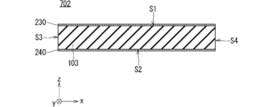
- ⁇ Third embodiment> 9 is a cross-sectional view illustrating a schematic configuration of a multilayer ceramic electronic component 702 according to the present embodiment 3.
- the ceramic portion 103 of the multilayer ceramic electronic component 702 may be similar to the ceramic portion 101 (FIG. 3) in the embodiment 1, the ceramic portion 102 (FIG. 7) in the embodiment 2, or any of the ceramic portions of the modifications thereof.
- the multilayer ceramic electronic component 702 also has a first electrode 230 and a second electrode 240 in place of the first electrode 210 and the second electrode 220 in the multilayer ceramic electronic component 701 (FIG. 2), respectively.
- the first electrode 230 is disposed on the first surface S1, and in the illustrated example, is disposed over substantially the entire first surface S1.
- the first electrode 230 does not need to be disposed on any surface other than the first surface S1.
- the second electrode 240 is disposed on the second surface S2, and in the illustrated example, is disposed over substantially the entire second surface S2.
- the second electrode 240 does not need to be disposed on any surface other than the second surface S2.
- the internal electrode layers 213 and 223 are also not required.
- ⁇ Fourth embodiment> 10 is a cross-sectional view illustrating a schematic configuration of a multilayer ceramic electronic component 703 according to the present embodiment 4.
- the ceramic portion 103 of the multilayer ceramic electronic component 703 may be similar to the ceramic portion 101 (FIG. 3) in the embodiment 1, the ceramic portion 102 (FIG. 7) in the embodiment 2, or any of the ceramic portions of the modifications thereof.
- the multilayer ceramic electronic component 702 has a first electrode 250 and a second electrode 260 instead of the first electrode 210 and the second electrode 220 in the multilayer ceramic electronic component 701 (FIG. 2).
- the first electrode 250 includes a portion 251 located on the first surface S1.
- the first electrode 250 includes a portion 254 located on the second surface S2 and a portion 252 located on a part of the third surface S3.
- the portion 251 is disposed on substantially the entire first surface S1.
- the second electrode 260 is disposed on the second surface S2 away from the first electrode 250.
- the second electrode 260 does not need to be disposed on any surface other than the second surface S2.
- the internal electrode layers 213 and 223 are not required.
- Example 1 which is a multilayer ceramic electronic component having ceramic part 101 (FIG. 3: embodiment 1)
- Examples 2A to 2C which are multilayer ceramic electronic components having ceramic part 102 (FIG. 3: embodiment 1)
- a comparative example which, unlike these examples, has flat first surface S1 and second surface S2, are shown below.
- the capacitance is shown as a difference with the comparative example as a reference.
- the capacitance was measured by applying a voltage of 1 kHz frequency and 1 V amplitude (0 ⁇ 0.5 V) while applying a pair of probe electrodes of an LCR meter to the first electrode 210 and second electrode 220 (see FIG. 1) on the first surface S1. From the above measurement results, it was found that each of the examples had a higher capacitance than the comparative example.
- Ceramic part 150 Green laminate 151 to 153: Green sheet 161, 162: Substrate 210, 230, 250: First electrode 213: First internal electrode layer 220, 240, 260: Second electrode 223: Second internal electrode layer 600: Work in progress 701 to 703: Multilayer ceramic electronic component 1100: Elastic member S1: First surface S2: Second surface
Landscapes
- Engineering & Computer Science (AREA)
- Power Engineering (AREA)
- Microelectronics & Electronic Packaging (AREA)
- Manufacturing & Machinery (AREA)
- Chemical & Material Sciences (AREA)
- Ceramic Engineering (AREA)
- Physics & Mathematics (AREA)
- Electromagnetism (AREA)
- Inorganic Chemistry (AREA)
- Fixed Capacitors And Capacitor Manufacturing Machines (AREA)
- Ceramic Capacitors (AREA)
Priority Applications (2)
| Application Number | Priority Date | Filing Date | Title |
|---|---|---|---|
| JP2025509932A JPWO2024202710A1 (https=) | 2023-03-30 | 2024-02-20 | |
| US19/341,569 US20260031276A1 (en) | 2023-03-30 | 2025-09-26 | Multilayered ceramic electronic component |
Applications Claiming Priority (2)
| Application Number | Priority Date | Filing Date | Title |
|---|---|---|---|
| JP2023055084 | 2023-03-30 | ||
| JP2023-055084 | 2023-03-30 |
Related Child Applications (1)
| Application Number | Title | Priority Date | Filing Date |
|---|---|---|---|
| US19/341,569 Continuation US20260031276A1 (en) | 2023-03-30 | 2025-09-26 | Multilayered ceramic electronic component |
Publications (1)
| Publication Number | Publication Date |
|---|---|
| WO2024202710A1 true WO2024202710A1 (ja) | 2024-10-03 |
Family
ID=92905122
Family Applications (1)
| Application Number | Title | Priority Date | Filing Date |
|---|---|---|---|
| PCT/JP2024/006012 Ceased WO2024202710A1 (ja) | 2023-03-30 | 2024-02-20 | 積層セラミック電子部品 |
Country Status (3)
| Country | Link |
|---|---|
| US (1) | US20260031276A1 (https=) |
| JP (1) | JPWO2024202710A1 (https=) |
| WO (1) | WO2024202710A1 (https=) |
Citations (5)
| Publication number | Priority date | Publication date | Assignee | Title |
|---|---|---|---|---|
| JP2001044066A (ja) * | 1999-07-30 | 2001-02-16 | Kyocera Corp | 積層型電子部品およびその製法 |
| WO2011145453A1 (ja) * | 2010-05-17 | 2011-11-24 | 株式会社村田製作所 | 圧電アクチュエータ及び駆動装置 |
| JP2014110417A (ja) * | 2012-12-04 | 2014-06-12 | Samsung Electro-Mechanics Co Ltd | 基板内蔵用積層セラミック電子部品及びその製造方法、基板内蔵用積層セラミック電子部品を備える印刷回路基板 |
| JP2020009949A (ja) * | 2018-07-10 | 2020-01-16 | 日本碍子株式会社 | 積層セラミック電子部品および電子部品組立体 |
| JP2022142240A (ja) * | 2021-03-16 | 2022-09-30 | 株式会社村田製作所 | 積層セラミックコンデンサ |
-
2024
- 2024-02-20 WO PCT/JP2024/006012 patent/WO2024202710A1/ja not_active Ceased
- 2024-02-20 JP JP2025509932A patent/JPWO2024202710A1/ja active Pending
-
2025
- 2025-09-26 US US19/341,569 patent/US20260031276A1/en active Pending
Patent Citations (5)
| Publication number | Priority date | Publication date | Assignee | Title |
|---|---|---|---|---|
| JP2001044066A (ja) * | 1999-07-30 | 2001-02-16 | Kyocera Corp | 積層型電子部品およびその製法 |
| WO2011145453A1 (ja) * | 2010-05-17 | 2011-11-24 | 株式会社村田製作所 | 圧電アクチュエータ及び駆動装置 |
| JP2014110417A (ja) * | 2012-12-04 | 2014-06-12 | Samsung Electro-Mechanics Co Ltd | 基板内蔵用積層セラミック電子部品及びその製造方法、基板内蔵用積層セラミック電子部品を備える印刷回路基板 |
| JP2020009949A (ja) * | 2018-07-10 | 2020-01-16 | 日本碍子株式会社 | 積層セラミック電子部品および電子部品組立体 |
| JP2022142240A (ja) * | 2021-03-16 | 2022-09-30 | 株式会社村田製作所 | 積層セラミックコンデンサ |
Also Published As
| Publication number | Publication date |
|---|---|
| JPWO2024202710A1 (https=) | 2024-10-03 |
| US20260031276A1 (en) | 2026-01-29 |
Similar Documents
| Publication | Publication Date | Title |
|---|---|---|
| KR101309326B1 (ko) | 적층 칩 전자부품, 그 실장 기판 및 포장체 | |
| KR101309479B1 (ko) | 적층 칩 전자부품, 그 실장 기판 및 포장체 | |
| CN103578758B (zh) | 片式层压电子元件、用于安装该元件的板件及其封装单元 | |
| KR101452054B1 (ko) | 적층 세라믹 커패시터 및 그 실장 기판 | |
| JPH08130160A (ja) | 積層セラミック電子部品の製造方法 | |
| KR101486979B1 (ko) | 적층 세라믹 전자부품의 제조방법 | |
| KR20150011263A (ko) | 적층 세라믹 커패시터 및 그 실장 기판 | |
| KR20140080019A (ko) | 적층 세라믹 커패시터 및 적층 세라믹 커패시터의 실장 기판 | |
| KR20140041235A (ko) | 적층 칩 전자부품, 그 실장 기판 및 포장체 | |
| TW201428792A (zh) | 多層式陶瓷電容器及用於該多層式陶瓷電容器的安裝板件 | |
| CN103915255A (zh) | 多层陶瓷电容器及用于多层陶瓷电容器的安装板 | |
| JP2020167198A (ja) | 積層セラミックコンデンサ | |
| US20200312568A1 (en) | Multilayer ceramic capacitor | |
| JP2015018891A (ja) | 積層セラミックコンデンサ | |
| KR20220040994A (ko) | 적층 세라믹 콘덴서 | |
| KR20140012577A (ko) | 적층 칩 전자부품, 그 실장 기판 및 포장체 | |
| WO2024202710A1 (ja) | 積層セラミック電子部品 | |
| JP6189742B2 (ja) | 積層型電子部品およびその製造方法 | |
| JPH11214244A (ja) | 積層セラミックコンデンサ | |
| JP2001044059A (ja) | 積層セラミックコンデンサ | |
| JP2004014668A (ja) | 積層セラミック電子部品の製造方法 | |
| JP2002299149A (ja) | 積層セラミックコンデンサ | |
| JPH05226178A (ja) | 積層セラミックコンデンサおよびその製造法 | |
| JP2015023262A (ja) | 積層セラミック電子部品の製造方法 | |
| KR101512601B1 (ko) | 적층 세라믹 커패시터 및 적층 세라믹 커패시터의 실장 기판 |
Legal Events
| Date | Code | Title | Description |
|---|---|---|---|
| 121 | Ep: the epo has been informed by wipo that ep was designated in this application |
Ref document number: 24778854 Country of ref document: EP Kind code of ref document: A1 |
|
| ENP | Entry into the national phase |
Ref document number: 2025509932 Country of ref document: JP Kind code of ref document: A |
|
| WWE | Wipo information: entry into national phase |
Ref document number: 2025509932 Country of ref document: JP |
|
| NENP | Non-entry into the national phase |
Ref country code: DE |
|
| 122 | Ep: pct application non-entry in european phase |
Ref document number: 24778854 Country of ref document: EP Kind code of ref document: A1 |