WO2024202254A1 - 積層構造体およびプリント基板 - Google Patents
積層構造体およびプリント基板 Download PDFInfo
- Publication number
- WO2024202254A1 WO2024202254A1 PCT/JP2023/043300 JP2023043300W WO2024202254A1 WO 2024202254 A1 WO2024202254 A1 WO 2024202254A1 JP 2023043300 W JP2023043300 W JP 2023043300W WO 2024202254 A1 WO2024202254 A1 WO 2024202254A1
- Authority
- WO
- WIPO (PCT)
- Prior art keywords
- resin substrate
- recess
- metal
- metal layer
- laminated structure
- Prior art date
- Legal status (The legal status is an assumption and is not a legal conclusion. Google has not performed a legal analysis and makes no representation as to the accuracy of the status listed.)
- Ceased
Links
Images






Classifications
-
- B—PERFORMING OPERATIONS; TRANSPORTING
- B32—LAYERED PRODUCTS
- B32B—LAYERED PRODUCTS, i.e. PRODUCTS BUILT-UP OF STRATA OF FLAT OR NON-FLAT, e.g. CELLULAR OR HONEYCOMB, FORM
- B32B15/00—Layered products comprising a layer of metal
- B32B15/04—Layered products comprising a layer of metal comprising metal as the main or only constituent of a layer, which is next to another layer of the same or of a different material
- B32B15/08—Layered products comprising a layer of metal comprising metal as the main or only constituent of a layer, which is next to another layer of the same or of a different material of synthetic resin
-
- H—ELECTRICITY
- H05—ELECTRIC TECHNIQUES NOT OTHERWISE PROVIDED FOR
- H05K—PRINTED CIRCUITS; CASINGS OR CONSTRUCTIONAL DETAILS OF ELECTRIC APPARATUS; MANUFACTURE OF ASSEMBLAGES OF ELECTRICAL COMPONENTS
- H05K3/00—Apparatus or processes for manufacturing printed circuits
- H05K3/38—Improvement of the adhesion between the insulating substrate and the metal
Definitions
- the present invention relates to a laminated structure and a printed circuit board.
- a method for manufacturing a copper-clad laminate is known in which a copper foil is pressure-bonded to a resin substrate. First, the copper foil is subjected to a roughening treatment to roughen the surface, and then the resin substrate is pressure-bonded to the roughened surface, thereby improving the adhesion between the copper foil and the resin substrate.
- Patent Documents 1 and 2 disclose copper foils that have been subjected to a roughening treatment (roughened copper foils).
- the roughened copper foil of Patent Document 1 is a roughened copper foil having a roughened surface on at least one side, the roughened surface comprising a plurality of primary roughening particles having a constricted portion, the primary roughening particles having a surface including the constricted portion with a plurality of secondary roughening particles smaller than the primary roughening particles, a secondary roughening particle density, which is the number of the secondary roughening particles in the constricted portion divided by the surface area of the constricted portion, is 9 to 30 particles/ ⁇ m2 , and the ten-point average roughness Rz of the roughened surface is 0.7 to 1.7 ⁇ m.
- the roughened copper foil of Patent Document 2 is a roughened copper foil having a roughened surface on at least one side on which a plurality of roughened particles are formed, the roughened particles have an uneven surface, the developed area ratio Sdr of the interface of the roughened surface measured using a three-dimensional white light interference microscope is 1000% or more and 5000% or less, and the arithmetic mean roughness Sa of the roughened surface is 0.04 ⁇ m or more and 0.6 ⁇ m or less.
- a copper-clad laminate produced using a roughened copper foil as described in Patent Documents 1 and 2 the adhesion (bonding strength) between the copper foil and the resin substrate is improved by the anchor effect.
- Such copper-clad laminates are mainly used in the manufacture of printed circuit boards.
- the copper foil of the copper-clad laminate is patterned by photolithography to form a wiring pattern.
- the resin surface is exposed, and on the exposed resin surface, a microstructure can be seen that is the transfer of the shape of the roughening particles from the roughening treatment applied to the copper foil.
- Patent Documents 1 and 2 the anchor effect is used to increase the bonding strength between the copper foil and the resin substrate, but the peeling of the wiring pattern when bending stress is applied to the printed circuit board is not considered.
- a first object of the present invention is to provide a laminated structure suitable for manufacturing printed circuit boards, which can suppress peeling of the wiring pattern when bending stress is applied to the printed circuit board.
- a second object of the present invention is to provide a printed circuit board capable of suppressing peeling of a wiring pattern due to bending stress.
- a resin substrate and a metal layer provided on a first surface of the resin substrate the resin substrate has a recess that opens on the first surface, and a stress relaxation structure on an inner surface of the recess;
- a laminate structure is provided, with a portion of the metal layer extending into the recess.
- a resin substrate and a metal wiring provided on a first surface of the resin substrate the resin substrate has a recess that opens on the first surface,
- a part of the metal wiring extends into the recess,
- the printed circuit board has a stress relaxation structure on the inner surface of the recess in the surface exposed area exposed from the metal wiring.
- Printed circuit boards manufactured from the laminated structure of the present invention can suppress peeling of the wiring pattern due to bending stress.
- FIG. 1 is a schematic perspective view of a laminated structure according to a first embodiment.
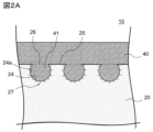
- FIG. 2A is a schematic enlarged cross-sectional view of the laminated structure taken along the line XX in FIG.
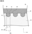
- FIG. 2B is a schematic enlarged cross-sectional view of the laminated structure taken along the line XX in FIG.
- FIG. 3 is a schematic enlarged cross-sectional view of a resin substrate included in the laminated structure of FIG. 2A.
- FIG. 4A is a schematic enlarged cross-sectional view of a portion enclosed by a dashed line in FIG. 3, and shows a schematic diagram of fine grooves formed on the inner surface of the recess.
- FIG. 4A is a schematic enlarged cross-sectional view of a portion enclosed by a dashed line in FIG. 3, and shows a schematic diagram of fine grooves formed on the inner surface of the recess.
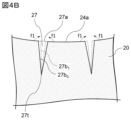
- FIG. 4B is a schematic enlarged cross-sectional view for explaining the change in shape of the narrow groove shown in FIG. 4A when a bending stress F1 is applied to the laminated structure shown in FIG.
- FIG. 4C is a schematic enlarged cross-sectional view for explaining a change in shape of the narrow groove shown in FIG. 4A when a bending stress F2 is applied to the laminated structure shown in FIG.
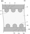
- FIG. 5 is a schematic diagram of an SEM image taken from the top surface direction of the resin substrate included in the laminate structure according to the first embodiment.
- FIG. 6A is a schematic enlarged cross-sectional view for explaining a method for manufacturing a laminated structure according to embodiment 2-1.
- FIG. 6B is a schematic enlarged cross-sectional view for explaining the method for manufacturing the laminated structure according to embodiment 2-1.
- FIG. 6C is a schematic enlarged cross-sectional view for explaining the method for manufacturing the laminated structure according to embodiment 2-1.
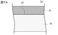
- FIG. 7A is a schematic enlarged cross-sectional view for explaining a method for manufacturing a laminated structure according to embodiment 2-2.
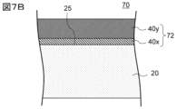
- FIG. 7B is a schematic enlarged cross-sectional view for explaining the method for manufacturing the laminated structure according to embodiment 2-2.
- FIG. 8A is a schematic enlarged cross-sectional view of a printed circuit board according to a third embodiment.
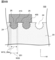
- FIG. 8B is a schematic enlarged cross-sectional view of the printed circuit board according to the third embodiment.
- FIG. 9 is a schematic enlarged cross-sectional view of a modified example of the laminated structure according to the first embodiment.
- FIG. 1 is a schematic perspective view of a laminated structure 10 according to an embodiment
- FIGS. 2A and 2B are schematic enlarged cross-sectional views of the laminated structure 10 in a cross-section along line X-X in FIG. 1 (a cross-section in the thickness direction of the resin substrate 20)
- FIG. 3 is a schematic enlarged cross-sectional view of the resin substrate 20 included in the laminated structure 10 in FIG. 2A.
- the laminated structure 10 includes a resin substrate 20 and a metal layer 40 provided on a first surface 25 of the resin substrate 20 .
- the resin substrate 20 has a recess 24 that opens to the first surface 25.
- a portion 41 of the metal layer 40 passes through the opening 26 of the recess 24 that opens to the first surface 25 and extends into the recess 24 of the resin substrate 20.
- the portion 41 of the metal layer 40 can function as an anchor that fixes the metal layer 40 to the resin substrate 20. In other words, the portion 41 of the metal layer 40 can improve the adhesion between the resin substrate 20 and the metal layer 40.
- the portion 41 of the metal layer 40 is usually filled with the metal material that constitutes the metal layer 40.
- air bubbles may be present inside the portion 41 of the metal layer 40. Air bubbles (or small cavities) may be present as long as the dimensions of the air bubbles (or small cavities) are sufficiently small compared to the dimensions of the portion 41 of the metal layer 40.
- width W1 of the part 41 of the metal layer 40 at the position of the first surface 25 of the resin substrate 20 is smaller than the maximum width W2 of the part 41 of the metal layer 40 inside the resin substrate 20.
- width W1 and “maximum width W2" each specify the dimensions measured in a direction (width direction: W direction) perpendicular to the thickness direction (T direction) of the resin substrate 20.
- the width W1 of the portion 41 of the metal layer 40 at the position of the first surface 25 is substantially equal to the width 26w of the opening 26 of the cavity 24 in the resin substrate 20 .
- the width W1 of the portion 41 of the metal layer 40 at the position of the first surface 25 is smaller than the maximum width W2 of the portion 41 of the metal layer 40 inside the resin substrate 20" has roughly the same meaning as the width 26w of the opening 26 of the cavity 24 being smaller than the maximum width W2 of the portion 41 of the metal layer 40.
- the portion 41 of the metal layer 40 can function as an anchor that fixes the metal layer 40 to the resin substrate 20. If the width 26w of the opening 26 is smaller than the maximum width W2 of the portion 41 of the metal layer 40 inside the resin substrate 20, the portion 41 of the metal layer 40 is unlikely to escape from the opening 26. In particular, if the width 26w is significantly smaller than the maximum width W2, the portion 41 of the metal layer 40 cannot escape from the opening 26. Therefore, the anchor effect of the portion 41 of the metal layer 40 is improved, and the adhesion between the resin substrate 20 and the metal layer 40 can be further improved.
- the laminated structure 10 according to the first embodiment has a stress relaxation structure on the inner surface 24a of the recess 24 in the resin substrate 20.
- the stress relaxation structure is, for example, a narrow groove 27 provided on the inner surface 24a of the recess 24 (see FIG. 4A).
- the term “narrow groove 27” refers to a narrow groove 27 having a length 27L of 0.05 ⁇ m or more in a top view (see FIG. 5) of the inner surface 24a of the recess 24, and a length 27L that is 20 times or more the width 27w of the narrow groove 27 (see FIG. 4A).
- the narrow groove 27 may not be linear in a top view.
- the length 27L of the narrow groove 27 refers to the maximum dimension of the continuous narrow groove 27 in a top view.
- the straight-line distance between both ends of the narrow groove 27i is the length 27L of the narrow groove 27i.
- the plurality of fine grooves 27ii are treated as a single unit.
- a region 27R in which the plurality of fine grooves 27ii exist is specified, and the maximum dimension of the plurality of fine grooves 27ii in the region 27R is set as the length 27L of the plurality of fine grooves 27ii.
- Fig. 4A is a schematic enlarged cross-sectional view of a portion surrounded by a dashed circle on the inner surface 24a of the recess 24 of the resin substrate 20 in Fig. 3.
- Fig. 4A shows a schematic view of a fine groove 27 formed on the inner surface 24a of the recess.
- narrow groove 27 has width 27w at opening 27a, and the width of narrow groove 27 from opening 27a to the deepest part of narrow groove 27 (referred to as innermost part 27t of narrow groove 27) is considered to be narrower than width 27w.
- innermost part 27t of narrow groove 27 is considered to be narrower than width 27w.
- narrow groove 27 may be a V-shaped groove whose width gradually narrows from opening 27a to innermost part 27t in a cross-sectional view.
- the inner surface 27b0 of the narrow groove 27 may be a flat surface, a curved surface, a rough surface, or the like.
- the narrow groove 27 may have a branch groove (not shown) provided on the inner surface 27b0 of the narrow groove 27.
- the branch groove is considered to have the widest opening width on the inner surface 27b0 , and the width of the branch groove from the opening to the innermost part of the branch groove is considered to be narrower than the opening width.
- the branch groove is usually smaller in length and opening width than the narrow groove 27.
- FIG. 3 is applied to the resin substrate 20 of the laminated structure 10 shown in Fig. 2A, the laminated structure 10 and the resin substrate 20 are curved in a downward convex direction, and a compressive stress is applied to the first surface 25 of the resin substrate 20.
- Fig. 4B shows the change in shape of the narrow groove 27 when the laminated structure 10 and the resin substrate 20 are subjected to the bending stress F1.
- a compressive stress f1 is applied to the narrow groove 27 (FIG. 3) provided on the inner surface 24a of the recess 24 that opens to the first surface 25 (FIG. 4B).
- the opening 27a of the narrow groove 27 is deformed so that its width becomes narrower.
- the inner surface of the narrow groove 27 is displaced from an inner surface 27b0 when no stress is applied to an inner surface 27b1 when compressive stress f1 is applied.
- Fig. 4C shows the change in shape of the narrow groove 27 when the laminated structure 10 and the resin substrate 20 are subjected to the bending stress F2.
- a tensile stress f2 is applied to the narrow groove 27.
- the opening 27a of the narrow groove 27 is deformed so as to widen.
- the inner surface of the narrow groove 27 is displaced from an inner surface 27b0 when no tensile stress f2 is applied to an inner surface 27b2 when a tensile stress is applied.
- the wiring-covered region 251 (the region where the first surface 25 is covered with the metal wiring 400) of the resin base material 20 also has a recess 24, and the inner surface 24a of the recess 24 has a stress relaxation structure (narrow groove 27).
- the stress relaxation structure (narrow groove 27) of the wiring-covered region 251 is less likely to deform than the stress relaxation structure (narrow groove 27) formed in the surface-exposed region 252.
- the wiring-covered region 251 of the first surface 25 is prevented from being deformed by bending stress, so that the metal wiring 400 formed on the surface of the wiring-covered region 251 can be effectively prevented from peeling off from the resin base material 20.
- the average width 27w of the narrow groove 27 on the inner surface 24a of the recess is preferably 0.1 nm to 100 nm, more preferably 0.1 nm to 10 nm.
- the average width of the narrow groove 27 refers to the arithmetic average value of the width 27w of the opening 27a of the narrow groove 27 measured at a plurality of positions. A detailed measurement method will be described below.
- the metal layer 40 is removed from the laminated structure 10 by etching or the like. Thereafter, the first surface 25 of the resin substrate 20 is pretreated in order to obtain an SEM image (for example, using JEC-3000FC manufactured by JEOL, pretreatment with Pt coat 20mA-30s).
- the inner surface 24a of the recess 24 is observed from the first surface 25 side (upper surface side) of the resin substrate 20 using a scanning electron microscope (for example, ultra-high resolution field emission scanning electron microscope SU8230 manufactured by Hitachi High-Tech Corporation).
- the conditions for SEM observation are an acceleration voltage of 3 kV and a magnification of 100,000 times.
- the obtained SEM image may be processed with image processing software (for example, image software built into the scanning electron microscope, or image processing software such as Photo 2019 manufactured by Microsoft) as necessary to adjust brightness, contrast, etc.
- image processing software for example, image software built into the scanning electron microscope, or image processing software such as Photo 2019 manufactured by Microsoft
- FIG. 5 is a schematic diagram of an SEM image of the inner surface 24a of the recess 24 of the resin substrate 20 included in the laminated structure 10 according to embodiment 1, taken from the first surface 25 side (top surface side).
- 3 to 5 narrow grooves 27 are selected, and the width of each narrow groove is measured at three locations. In other words, 9 to 15 pieces of width measurement data are obtained from one SEM image.
- SEM images are obtained at different positions on the first surface 25 of the resin substrate 20, and the width of the narrow grooves 27 is measured. Three or more SEM images are obtained, the width of the narrow grooves 27 is measured, and the obtained width measurements are arithmetically averaged. In this manner, the average width of the narrow grooves 27 is obtained.
- the depth 27d of the narrow groove 27 (see FIG. 4A) is considered to be approximately equal to the width 27w of the narrow groove 27 at the opening 27a.
- the narrow groove 27 is formed by the metal elements constituting the metal layer 40 (more precisely, the second metal layer 40y in FIG. 6C) diffusing (penetrating) from the first surface 25 of the resin substrate 20.
- the narrow groove 27 is considered to grow isotropically in the width direction and the depth direction, and it is presumed that the width 27w and the depth 27d of the narrow groove 27 are approximately equal.
- the depth 27d of the narrow groove 27 refers to the distance from the opening 27a of the narrow groove 27 to the innermost part 27t (FIG. 4A). Please note that FIG. 4A is a schematic diagram, and therefore the dimensional relationship between the depth 27d and the width 27w of the narrow groove 27 differs from the actual one.
- the average value (average depth) of the depth 27d of the fine grooves 27 is preferably 0.1 nm or more and 100 nm or less, and more preferably 0.1 nm or more and 10 nm or less, the same as the average width of the fine grooves 27. If it is in this range, it is expected that the strength of the resin substrate 20 can be maintained while effectively exerting the stress relaxation effect.
- the laminated structure 10 ⁇ may include metal layers 40, 40 ⁇ on both sides of the resin base material 20 (see FIG. 9).
- 9 includes a metal layer 40 on a first surface 25 of a resin substrate 20, as in the case of FIG. 1 and FIG. 2A, and further includes a second metal layer 40 ⁇ on a second surface 25 ⁇ opposite to the first surface 25.
- the resin substrate 20 has a second recess 24 ⁇ that opens to the second surface 25 ⁇ , and has a stress relaxation structure (narrow groove 27) on the inner surface of the second recess 24 ⁇ .
- a portion 41 ⁇ of the second metal layer 40 ⁇ extends into the second recess 24 ⁇ .
- the laminated structure 10 ⁇ is suitable for producing a printed circuit board having metal wiring on both sides.
- Embodiment 2 Manufacturing method of laminated structure 10.
- a method for manufacturing the laminated structure 10 (see FIGS. 1 and 2A) according to the embodiment 1 will be described.
- the method for manufacturing the laminated structure 10 is not limited to this, but two examples can be given. These manufacturing methods will be described in detail in each of the embodiments 2-1 and 2-2.
- the first method for manufacturing the laminated structure 10 includes the steps of: 1) modifying the surface of the first surface 25 of the resin substrate 20; 2) after the surface modification, a step of forming a metal precursor 62 containing a first metal element and a second metal element on the first surface 25 of the resin substrate 20 to prepare a precursor laminate 60; and 3) a step of heating the precursor laminate 60.
- the recess 24 in the resin substrate 20 is formed in step 3) by heating the precursor laminate 60.
- the narrow groove 27 on the inner surface 24a of the recess 24 is formed by modifying the surface of the first surface 25 of the resin substrate 20 in step 1) and then heating the precursor laminate 60 in step 3).
- Step 1) Step of surface-modifying the first surface 25 of the resin substrate 20
- a resin substrate 20 having no recesses 24 is prepared, and the first surface 25 is surface-modified.
- One example of the surface modification is ultraviolet irradiation (UV irradiation), in which the first surface 25 of the resin substrate 20 is modified by irradiating it with ultraviolet (UV) rays.
- UV irradiation ultraviolet irradiation
- step 3 When modifying the first surface 25 by UV irradiation, the UV reacts with oxygen in the air to generate ozone, which breaks some of the chemical bonds of the molecules of the resin material that makes up the resin substrate 20 on the surface of the first surface 25 (degradation of the molecules).
- step 3) described below, the metal elements that make up the second metal layer 40y are likely to thermally diffuse in the areas where the chemical bonds have been broken.
- cracks (narrow grooves 27) are formed on the first surface 25 of the resin substrate 20.
- the cracks (narrow grooves 27) caused by the diffusion of the metal elements extend toward the inside of the resin substrate 20 as the diffusion of the metal elements progresses further.
- step 3 recesses 24 are formed on the first surface 25 of the resin substrate 20, and the recesses 24 further expand into the resin substrate 20.
- the speed at which the narrow grooves 27 expand inward is greater than or equal to the speed at which the recesses 24 expand, so the narrow grooves 27 do not disappear and remain on the inner surface 24a of the recesses 24.
- the resin substrate 20 has recesses 24 that open to the first surface 25, and narrow grooves 27 formed on the inner surface 24a of the recesses 24.
- methods of surface modification include plasma treatment, corona treatment, electron beam irradiation, and treatment using chemicals such as oxidizers. All of these methods can modify the first surface 25 of the resin substrate 20 and break some of the chemical bonds of the molecules of the resin material that constitutes the resin substrate 20.
- the depth of modification is preferably a certain degree of depth.
- the modification depth corresponds to the thickness of the modified layer obtained after modification.
- the thickness of the modified layer can be, for example, about 0.001 ⁇ m to 1 ⁇ m.
- the modification treatment by UV irradiation is irradiation with a low pressure mercury lamp (MHU-110BK manufactured by Multiply Corporation, dominant wavelength: 254 nm) at an illuminance of 9.54 mW/cm 2 ⁇ 10 minutes.
- the metal precursor 62 has a two-layer structure including a first metal layer (referred to as "barrier film 40x") containing a first metal element disposed on the resin substrate 20, and a second metal layer 40y containing a second metal element disposed on the barrier film 40x.
- the barrier film 40x and the second metal layer 40y are collectively referred to as the "metal layer 40".
- the metal precursor 62 is formed by sequentially laminating a barrier film 40x and a second metal layer 40y on the resin base material 20.
- the barrier film 40x is formed by forming a film of a metal material containing a first metal element on the first surface 25 of the resin base material 20 by, for example, electroless plating, sputtering, etc.
- the second metal layer 40y is formed by forming a film of a metal material containing a second metal element on the surface 40xb of the barrier film 40x by, for example, electroless plating, sputtering, etc.
- the barrier film 40x is formed on the resin substrate 20 by electroless plating, it is preferable to pretreat the first surface 25 of the resin substrate 20 by a known pretreatment method such as providing a catalyst.
- the first metal element contained in the barrier film 40x and the second metal element contained in the second metal layer 40y have different diffusion coefficients in the resin base material 20, and that the diffusion coefficient of the first metal element in the resin base material 20 is smaller than the diffusion coefficient of the second metal element. Since the second metal element has a relatively large diffusion coefficient in the resin substrate 20, the second metal layer 40y containing the second metal element preferentially diffuses into the resin substrate 20 by the heating process. Thus, the extension portion 44 (see FIG. 6C ) can be easily formed from the second metal layer 40y. The extension portion 44 corresponds to the part 41 (see FIG. 2A ) of the metal layer 40 in the first embodiment.
- the barrier film 40x containing the first metal element is less likely to diffuse into the resin substrate 20 even during the heating process, and the shape of the film is easily maintained. In other words, even after process 3), the barrier film 40x is likely to remain between the resin substrate 20 and the second metal layer 40y. In other words, the barrier film 40x allows a portion 41 of the second metal layer 40y to diffuse into the resin substrate 20, but prevents the entire second metal layer 40y from diffusing into the resin substrate 20. In this way, the small diffusion coefficient of the first metal element makes it possible to form a barrier film 40x with high barrier function.
- the first metal element is preferably one or more selected from the group consisting of Fe, V, Ni, Ti, Ca, Ag, Zn, Al, Mg, Rh, Pt, Au, and Pd
- the second metal element is preferably one or more selected from the group consisting of Co, Mn, and Cu.
- the material for forming the barrier film 40x may consist of only the first metal element, or may further contain other elements in addition to the first metal element as long as the barrier function of the barrier film 40x is not impaired.
- the material for forming the second metal layer 40y may consist only of the second metal element, or may further contain other elements in addition to the second metal element as long as the formation of the narrow groove 27 and the extension portion 44 is not hindered.
- the average thickness of the barrier film 40x before step 3 i.e., the average thickness when the barrier film 40x is formed, is not particularly limited, but can be, for example, 10 nm or more and 100 nm or less. If the thickness of the barrier film 40x is 10 nm or more, the barrier function of the barrier film 40x can be fully exerted. If the thickness is 100 nm or less, the through-hole 32 penetrating the barrier film 40x can be easily formed in step 3).
- the average thickness of the barrier film 40x after step 3 i.e., the average thickness of the barrier film 40x in the laminated structure 10, is more preferably 0.005 ⁇ m or more and 1 ⁇ m or less, and particularly preferably 0.01 ⁇ m or more and 0.1 ⁇ m or less.
- the thickness of the barrier film 40x is measured at any five points, and the arithmetic mean value of the measured values is taken as the average thickness of the barrier film 40x.
- the resin substrate 20 may be, for example, acrylonitrile butadiene styrene (ABS), polycarbonate/acrylonitrile butadiene styrene (PC/ABS), acrylonitrile styrene acrylate (ASA), silicone-based composite rubber-acrylonitrile-styrene (SAS), Noryl, polypropylene, polycarbonate (PC), polycarbonate-based alloy, acrylonitrile styrene, polyacetate, polylactic acid, polystyrene, polyamide, aromatic polyamide, polyethylene, polyether ketone, polyethylene terephthalate, polybutene, polypropylene ...
- ABS acrylonitrile butadiene styrene
- PC/ABS polycarbonate/acrylonitrile butadiene styrene
- AS acrylonitrile styrene acrylate
- Noryl polypropylene
- PC polycarbonate
- PC polycarbonate-based
- the polymer may include one or more selected from the group consisting of ethylene terephthalate, polysulfone, polyether ether sulfone, polyetherimide, modified polyphenylene ether, polyphenylene sulfide, polyphenylene oxide, polyamide, polyimide, modified polyimide, epoxy resin, cycloolefin polymer, polynorbornene, perfluoroalkoxy fluorine polymer, polytetrafluoroethylene, vinylidene fluoride, vinyl resin, phenol resin, polyacetal, nylon, liquid crystal polymer, etc., and copolymers of each of the above polymers.
- Step 3 Heating the precursor laminate 60
- a part of the second metal layer 40y penetrates the barrier film 40x, which was a continuous film, and further diffuses into the resin substrate 20. At this time, the diffusion occurs while forming cracks (narrow grooves 27) in the resin substrate 20.
- a part of the second metal layer 40y diffuses further into the resin substrate 20, and can form an extension portion 44 as shown in Fig. 6C.
- step 3 the first metal element contained in the barrier film 40x and the second metal element contained in the second metal layer 40y are mutually thermally diffused, and through holes 32 are formed in the barrier film 40x.
- the formation of the through holes 32 is presumably influenced by structural defects in the barrier film 40x, variations in the size of the crystal grains forming the barrier film 40x, and co-deposition of contamination in the barrier film 40x (these are referred to as "structural defects in the barrier film 40x").
- structural defects in the barrier film 40x In the portion of the barrier film 40x where structural defects exist, the diffusion speed of the metal elements between the first metal element and the second metal element is expected to be faster than in the portion where no structural defects exist.
- the diffusion of the metal elements is locally promoted, so that the barrier film 40x becomes locally thin, and finally the through holes 32 are formed. Since the structural defects in the barrier film 40x occur randomly in the barrier film 40x, the through holes 32 are also randomly formed at positions corresponding to the positions of the structural defects.
- the through-hole 32 When the through-hole 32 is formed in the barrier film 40x, a part of the second metal layer 40y contacts the first surface 25 of the resin substrate 20 through the through-hole 32.
- the metal elements constituting the second metal layer 40y start to diffuse into the first surface 25 of the resin substrate 20 softened by heating (FIG. 6B), and a narrow groove 27 is formed on the first surface 25.
- the diffusion of the metal elements progresses with the heating time, and a part of the second metal layer 40y extends into the resin substrate 20.
- a part of the second metal layer 40y further spreads into the resin substrate 20 while pushing out the resin material constituting the resin substrate 20, forming an extension part 44 (FIG. 6C).
- an extension part 44 On the surface of the extension part 44, a wedge-shaped protrusion penetrating into the narrow groove 27 may be present. It is presumed that such a mechanism results in the laminated structure 10 shown in FIG. 6C.
- the heating conditions for step 3) are, for example, a heating temperature greater than (Tm-30)°C and less than Tm°C, and a heating time greater than or equal to 1 minute and less than or equal to 120 minutes.
- Tm (°C) is the melting point of the resin material used in the resin substrate 20.
- the melting point of the mixed material is measured or calculated and used as Tm.
- the resin substrate 20 is formed by laminating multiple resin sheets made of different resin materials, the melting point of the resin material of the resin sheet in contact with the metal precursor 62 is used as Tm.
- the heating conditions can affect the dimensions of the through-holes 32 in the barrier film 40x and the dimensions and shape of the recesses 24 in the resin substrate 20 (i.e., the dimensions and shape of the extensions 44 of the second metal layer 40y).
- the extensions 44 can be made to have dimensions and shapes suitable for functioning as an anchor that fixes the second metal layer 40y to the resin substrate 20.
- the heating temperature is excessively high or the heating time is excessively long, there is a risk that the barrier film 40x will disappear entirely. Without the barrier film 40x, the entire second metal layer 40y will diffuse into the resin substrate 20, and a structure having an anchor function (extension portion 44 in FIG. 6C) will not be formed, and there is a risk that the effect of improving the adhesion between the resin substrate 20 and the second metal layer 40y will not be obtained.
- the laminated structure 10 shown in Figures 2A and 6C is obtained by the first manufacturing method.
- Embodiment 2-2 Second manufacturing method of laminated structure 10.
- the second manufacturing method of the laminated structure 10 mainly differs from the first manufacturing method in the structure and formation method of the metal precursor formed in step 2). The rest is the same as the first manufacturing method.
- the second manufacturing method described in embodiment 2-2 will be described mainly with respect to the differences from the first manufacturing method, and the description of the same matters as the first manufacturing method (e.g., step 1)) may be omitted.
- FIG. 7A and 7B are schematic enlarged cross-sectional views for explaining a second manufacturing method of the laminated structure 10.
- the second manufacturing method of the laminated structure 10 includes, in step 2), a step of heating a precursor laminate 70 including the resin substrate 20 after the first surface 25 has been surface-modified and a metal precursor 72 including a first metal element and a second metal element located on the first surface 25 of the resin substrate 20.
- the metal precursor 72 formed in step 2) is a single plating layer disposed on the resin substrate 20. This plating layer includes a first metal element and a second metal element.
- the metal precursor 72 consisting of a single plating layer can be formed by electroless plating. Known plating solutions, plating conditions, etc. used in the electroless plating can be applied. Before electroless plating, it is preferable to pretreat the first surface 25 of the resin substrate 20 by a known pretreatment method such as providing a catalyst.
- the precursor laminate 70 obtained by forming a metal precursor 72 consisting of a single plating layer on the first surface 25 of the resin substrate 20 is subjected to step 3) under the same conditions as in the first manufacturing step.
- the metal precursor 72 becomes a two-layer structure consisting of a barrier film 40x containing a first metal element located on the resin substrate 20, and a second metal layer 40y containing a second metal element located on the barrier film 40x (see FIG. 7B).
- the two-layer structure of the barrier film 40x and the second metal layer 40y can be achieved by the phenomenon in which the first metal element in the metal precursor 72 segregates to the first surface 25 of the resin substrate 20. Although the mechanism of this segregation phenomenon is unclear, it is presumed that the first metal element in the metal precursor 72 diffuses in all directions upon heating, and is fixed to the first surface 25 when it reaches the first surface 25 of the resin substrate 20. As a result, the first metal element segregates to the first surface 25 of the resin substrate 20, becoming the barrier film 40x.
- a through hole 32 is formed in the barrier film 40x, which was a continuous film, as in the first manufacturing method of embodiment 2-1, and a part of the second metal layer 40y can extend through the through hole 32 into the inside of the resin substrate 20 to form an extension portion 44 ( Figures 6B and 6C).
- the heating step in step 3) may be divided into two stages (preheating and main heating).
- a preheating step is performed in which the metal precursor 72 consisting of a single plating layer is heated at 190° C. or more and 210° C. or less in order to form the metal precursor 72 into a two-layer structure consisting of the barrier film 40x and the second metal layer 40y, and then main heating is performed under the same heating conditions as in step 3) in the first manufacturing method described in embodiment 2-1.
- the preheating time is arbitrary, but may be, for example, 30 minutes or more and 90 minutes or less.
- the preferred heating conditions (heating temperature and heating time) in step 3), the preferred relationship between the diffusion coefficients of the first metal element and the second metal element, the types of metal elements suitable for the first metal element and the second metal element, the type of resin material suitable for the resin substrate 20, etc. are the same as those in the first manufacturing method described in embodiment 2-1.
- the laminated structure 10 shown in Figures 2A and 6C is obtained by the second manufacturing method.
- the printed circuit board 100 includes a resin base material 20 and a metal wiring 400 provided on a first surface 25 of the resin base material 20.
- the resin base material 20 has a recess 24 that opens on the first surface 25.
- the resin base material 20 includes a wiring-covered region 251 in which the first surface 25 is covered with the metal wiring 400, and a surface-exposed region 252 in which the metal wiring 400 is removed and the first surface 25 is exposed from the metal wiring 400. In the wiring-covered region 251, a part 410 of the metal wiring 400 extends into the recess 24 through the opening 26.
- the inner surface 24a of the recess 24 is exposed, and a stress relaxation structure (narrow groove 27) is formed on the inner surface 24a. Note that the stress relaxation structure (narrow groove 27) may also be present on the inner surface 24a of the recess 24 in the wiring-covered region 251.
- the stress relaxation structure can relax bending stress generated in the laminated structure 10.
- the stress relaxation structure (narrow groove 27) of the inner surface 24a of the recess 24 in the surface exposed region 252 is preferentially deformed to relieve the bending stress applied to the printed circuit board 100.
- the inner surface 24a of the recess 24 is in contact with a part 410 of the metal wiring 400, and therefore is less likely to deform than the stress relaxation structure (narrow groove 27) of the recess 24 formed in the surface exposed region 252.
- the stress relaxation structure (narrow groove 27) of the recess 24 formed in the surface exposed region 252 is preferentially deformed to relieve stress. Since the metal wiring 400 is not present in the surface exposed region 252, even if the stress relaxation structure (narrow groove 27) is deformed, this is unlikely to cause peeling of the metal wiring 400. On the other hand, the stress relaxation structure (narrow groove 27) of the recess 24 formed in the wiring covering region 251 is not easily subjected to bending stress (i.e., the stress relaxation structure (narrow groove 27) is not easily deformed), so peeling of the metal wiring 400 can be suppressed.
- the printed circuit board 100 of the third embodiment may have branched grooves on the inner surface of the narrow groove 27, similar to the laminated structure 10 of the first embodiment.
- the shape, average width, average depth, etc. of the fine groove 27 and the branch grooves are similar to those of the fine groove 27 and the branch grooves described in the first embodiment, and therefore detailed description is omitted.
- the width W10 (substantially equal to the width 26w of the opening 26) of the portion 410 of the metal wiring 400 at the position of the first surface 25 of the resin substrate 20 is smaller than the maximum width W20 of the portion 410 of the metal wiring 400 inside the resin substrate 20.
- the width W10 (corresponding to the width 26w of the opening 26) of the portion 410 of the metal wiring 400 is smaller than the maximum width W20 of the portion 410 of the metal wiring 400 inside the resin base material 20, the portion 410 of the metal wiring 400 is unlikely to escape from the opening 26.
- the width 26w is significantly smaller than the maximum width W20, the portion 410 of the metal wiring 400 cannot escape from the opening 26. Therefore, the anchor effect of the portion 410 of the metal wiring 400 is improved, and the adhesion between the resin base material 20 and the metal wiring 400 can be improved.
- a portion 410 of the metal wiring 400 of the printed circuit board 100 corresponds to a portion 41 of the metal layer 40 of the laminated structure 10
- the width W10 and maximum width W20 of the portion 410 of the metal wiring 400 correspond to the width W1 and maximum width W2 of the portion 41 of the metal layer 40, respectively.
- air bubbles or small cavities may be present inside the portion 410 of the metal wiring 400 .
- the printed circuit board using the laminated structure 10 ⁇ may include metal wiring 400 on both the first surface 25 and the second surface 25 ⁇ of the resin base material 20. That is, the resin base material 20 includes a second metal wiring on the second surface 25 ⁇ facing the first surface 25 of the resin base material 200, and the resin base material 20 has a second recess 24 ⁇ opening on the second surface 25 ⁇ , and in the second wiring covered region of the second surface 25 ⁇ covered with the second metal wiring, a part of the second metal wiring extends into the second recess 24 ⁇ , and in the second surface exposed region exposed from the second metal wiring, the inner surface of the second recess 24 ⁇ may have a stress relaxation structure (narrow groove 27).
- Such a printed circuit board includes metal wiring on both sides, and the metal wiring is unlikely to peel off from the resin base material 20 on either side.
- the printed circuit board 100 of embodiment 3 can be manufactured by using the laminated structure 10 of embodiment 1 and patterning the metal layer 40 by a conventionally known method (e.g., photolithography) to produce the metal wiring 400.
- a conventionally known method e.g., photolithography
- MHU-110BK low pressure mercury lamp
- pretreatment of the resin substrate 20 before producing the metal precursor 72 (treatment Nos. 1 to 5) and electroless plating (treatment No. 6) for producing the metal precursor 72 were performed to produce 10 samples of the precursor laminate 70.
- the obtained sample of the precursor laminate 70 was preheated at 200° C. for 60 minutes (treatment No. 7), and further heated at 300° C. for 10 minutes (treatment No. 8).
- the metal layer 40 was removed from the obtained laminated structure 10, and the inner surface 24a of the recess 24 was observed with an SEM from the first surface 25 side of the resin substrate 20.
- the conditions for the SEM observation were as follows. Pretreatment: JEOL JEC-3000FC, pretreatment with Pt coat 20mA-30s Scanning electron microscope (SEM)/energy dispersive X-ray fluorescence analyzer (EDX): Hitachi High-Tech Corporation, ultra-high resolution field emission scanning electron microscope SU8230, accelerating voltage 3kV, magnification 100,000x (x100k)/Bruker A.X. Co., Ltd. EDX for SEM XFlash 5060FQ
- the width of the narrow grooves 27 was measured using the length measurement function of the imaging software (Hitachi SU8200 Scanning Electron Microscope) built into the scanning electron microscope. In cases where the narrow grooves 27 on the inner surface 24a of the recesses 24 were difficult to see, the brightness, contrast, etc. were adjusted using the imaging software mentioned above or another image processing software (for example, Photo 2019 manufactured by Microsoft). A schematic diagram of one of the obtained SEM images is shown in Figure 5.
- a plurality of crack-like narrow grooves 27 were found on the inner surface 24a of the recess 24. These narrow grooves 27 had an average width of about 1.25 nm. It is believed that forming a printed circuit board 100 from this laminated structure 10 will have a high stress relaxation ability and will be able to sufficiently prevent peeling of the metal wiring.
- Comparative Example 1 As Comparative Example 1, a commercially available copper-clad laminate (former Panasonic Electric Works Co., Ltd., glass epoxy copper-clad laminate R1705) was prepared. After removing the copper foil from the copper-clad laminate, the surface of the glass epoxy substrate was observed with an SEM. The conditions for SEM observation were the same as those for Example 1.
- the recesses were roughly divided into three types based on their dimensions. The three sizes of recesses are considered to correspond to the recesses formed by primary particles (largest particles), secondary particles (medium-sized particles), and tertiary particles (smallest particles) attached to the roughened surface of the copper foil.
- each of the three recesses were as follows: Diameter of the largest recess (corresponding to the primary particle): Approximately 3.0 ⁇ m Diameter of medium-sized recesses (corresponding to secondary particles): Approximately 1.0 to 1.5 ⁇ m Diameter of the smallest recess (corresponding to a tertiary particle): Approximately 25 to 50 nm
- each recess was circular, and there was no recess corresponding to the "narrow groove 27" of the present invention. Therefore, when a printed circuit board was formed, it is believed that the stress relaxation ability was low and peeling of the metal wiring could not be sufficiently suppressed.
- ⁇ 2> The laminated structure according to ⁇ 1>, wherein the stress relaxation structure is a narrow groove provided on an inner surface of the recess.
- ⁇ 4> a second metal layer on a second surface of the resin substrate opposite to the first surface, the resin substrate has a second recess that opens on the second surface, and a stress relaxation structure on an inner surface of the second recess;
- the laminated structure according to any one of ⁇ 1> to ⁇ 3>, wherein a portion of the second metal layer extends into the second recess.
- ⁇ 5> ⁇ 4> The laminated structure according to any one of ⁇ 1> to ⁇ 4>, wherein, in a cross-sectional view in a thickness direction of the resin substrate, a width of a portion of the metal layer at the position of the first surface of the resin substrate is smaller than a maximum width of the portion of the metal layer inside the resin substrate.
- a resin substrate and a metal wiring provided on a first surface of the resin substrate the resin substrate has a recess that opens on the first surface, Of the first aspect, In the wiring covered region covered with the metal wiring, a part of the metal wiring extends into the recess, The printed circuit board has a stress relaxation structure on the inner surface of the recess in the surface exposed area exposed from the metal wiring.
- a part of the second metal wiring extends into the second recess,
- a width of a portion of the metal wiring at the position of the first surface of the resin base material is smaller than a maximum width of a portion of the metal wiring inside the resin base material.
Landscapes
- Engineering & Computer Science (AREA)
- Manufacturing & Machinery (AREA)
- Microelectronics & Electronic Packaging (AREA)
- Laminated Bodies (AREA)
Priority Applications (2)
| Application Number | Priority Date | Filing Date | Title |
|---|---|---|---|
| JP2025509710A JPWO2024202254A1 (https=) | 2023-03-31 | 2023-12-04 | |
| CN202380096736.0A CN121038955A (zh) | 2023-03-31 | 2023-12-04 | 层叠结构体和印刷基板 |
Applications Claiming Priority (2)
| Application Number | Priority Date | Filing Date | Title |
|---|---|---|---|
| JP2023058789 | 2023-03-31 | ||
| JP2023-058789 | 2023-03-31 |
Publications (1)
| Publication Number | Publication Date |
|---|---|
| WO2024202254A1 true WO2024202254A1 (ja) | 2024-10-03 |
Family
ID=92903883
Family Applications (1)
| Application Number | Title | Priority Date | Filing Date |
|---|---|---|---|
| PCT/JP2023/043300 Ceased WO2024202254A1 (ja) | 2023-03-31 | 2023-12-04 | 積層構造体およびプリント基板 |
Country Status (3)
| Country | Link |
|---|---|
| JP (1) | JPWO2024202254A1 (https=) |
| CN (1) | CN121038955A (https=) |
| WO (1) | WO2024202254A1 (https=) |
Citations (6)
| Publication number | Priority date | Publication date | Assignee | Title |
|---|---|---|---|---|
| JPH06143491A (ja) * | 1992-11-06 | 1994-05-24 | Mitsubishi Shindoh Co Ltd | 導電性積層フィルムおよびその製造方法 |
| US5599592A (en) * | 1994-01-31 | 1997-02-04 | Laude; Lucien D. | Process for the metallization of plastic materials and products thereto obtained |
| JP2004307980A (ja) * | 2003-04-10 | 2004-11-04 | Toray Eng Co Ltd | 金属張り液晶ポリエステル基材の製造方法 |
| JP2006135179A (ja) * | 2004-11-08 | 2006-05-25 | Hitachi Maxell Ltd | 配線基板用フィルム基材の作製方法及びフレキシブルプリント基板 |
| JP2006351646A (ja) * | 2005-06-14 | 2006-12-28 | Tokai Rubber Ind Ltd | 回路基板およびその製造方法 |
| JP2008221488A (ja) * | 2007-03-08 | 2008-09-25 | Kanto Gakuin Univ Surface Engineering Research Institute | 液晶ポリマーフィルム金属張積層板 |
-
2023
- 2023-12-04 JP JP2025509710A patent/JPWO2024202254A1/ja active Pending
- 2023-12-04 WO PCT/JP2023/043300 patent/WO2024202254A1/ja not_active Ceased
- 2023-12-04 CN CN202380096736.0A patent/CN121038955A/zh active Pending
Patent Citations (6)
| Publication number | Priority date | Publication date | Assignee | Title |
|---|---|---|---|---|
| JPH06143491A (ja) * | 1992-11-06 | 1994-05-24 | Mitsubishi Shindoh Co Ltd | 導電性積層フィルムおよびその製造方法 |
| US5599592A (en) * | 1994-01-31 | 1997-02-04 | Laude; Lucien D. | Process for the metallization of plastic materials and products thereto obtained |
| JP2004307980A (ja) * | 2003-04-10 | 2004-11-04 | Toray Eng Co Ltd | 金属張り液晶ポリエステル基材の製造方法 |
| JP2006135179A (ja) * | 2004-11-08 | 2006-05-25 | Hitachi Maxell Ltd | 配線基板用フィルム基材の作製方法及びフレキシブルプリント基板 |
| JP2006351646A (ja) * | 2005-06-14 | 2006-12-28 | Tokai Rubber Ind Ltd | 回路基板およびその製造方法 |
| JP2008221488A (ja) * | 2007-03-08 | 2008-09-25 | Kanto Gakuin Univ Surface Engineering Research Institute | 液晶ポリマーフィルム金属張積層板 |
Also Published As
| Publication number | Publication date |
|---|---|
| JPWO2024202254A1 (https=) | 2024-10-03 |
| CN121038955A (zh) | 2025-11-28 |
Similar Documents
| Publication | Publication Date | Title |
|---|---|---|
| JP5629002B2 (ja) | 印刷回路基板及びその製造方法 | |
| US9894765B2 (en) | Printed wiring board and method for producing printed wiring board | |
| CN1929721A (zh) | 用于在绝缘树脂层上形成配线的方法 | |
| WO2001074585A1 (en) | Metallized polyimide film | |
| KR101133488B1 (ko) | 무접착제 플렉시블 라미네이트 및 그 제조 방법 | |
| JP2003309355A (ja) | 印刷回路構造および回路基板を積層する方法 | |
| KR20110003267A (ko) | 플렉서블 동박 적층판 및 cof용 플렉서블 프린트 배선판, 그리고 이들의 제조 방법 | |
| WO2016063757A1 (ja) | 樹脂フィルム、プリント配線板用カバーレイ、プリント配線板用基板及びプリント配線板 | |
| JP2023030040A (ja) | プリント配線板の製造方法 | |
| CN1612678A (zh) | 多层印刷电路板及其制造方法 | |
| WO2024202254A1 (ja) | 積層構造体およびプリント基板 | |
| WO2009122589A1 (ja) | 2枚合わせ片面金属箔張積層板およびその製造方法、ならびに、片面プリント配線板およびその製造方法 | |
| US20200315002A1 (en) | Wiring substrate | |
| US7807066B2 (en) | Method of manufacturing a porous resin substrate having perforations and method of making a porous resin substrate including perforations having electrically conductive wall faces | |
| JP2018195599A (ja) | 配線板及びその製造方法 | |
| CN1836472A (zh) | 印刷布线板及其制造方法 | |
| TW201116181A (en) | Trench substrate and method of fabricating the same | |
| US12532413B2 (en) | Printed wiring board | |
| JP7201405B2 (ja) | 多層配線板の製造方法 | |
| TW200930201A (en) | Printed circuit board and method for manufacturing the same | |
| CN118339021A (zh) | 层叠结构体及其制造方法 | |
| US20120145447A1 (en) | Via structure, method for forming the via structure, and circuit board with the via structure and method for manufacturing the circuit board | |
| TW202135608A (zh) | 硬式電路板的製造方法 | |
| WO2025115840A1 (ja) | 表面処理銅箔、キャリア付き銅箔、銅張積層板、およびプリント配線基板 | |
| WO2022264378A1 (ja) | 配線基板の製造方法及び積層板 |
Legal Events
| Date | Code | Title | Description |
|---|---|---|---|
| 121 | Ep: the epo has been informed by wipo that ep was designated in this application |
Ref document number: 23930879 Country of ref document: EP Kind code of ref document: A1 |
|
| ENP | Entry into the national phase |
Ref document number: 2025509710 Country of ref document: JP Kind code of ref document: A |
|
| WWE | Wipo information: entry into national phase |
Ref document number: 2025509710 Country of ref document: JP |
|
| NENP | Non-entry into the national phase |
Ref country code: DE |
|
| 122 | Ep: pct application non-entry in european phase |
Ref document number: 23930879 Country of ref document: EP Kind code of ref document: A1 |