WO2024201833A1 - ショートバー、実装構造部およびユニット - Google Patents
ショートバー、実装構造部およびユニット Download PDFInfo
- Publication number
- WO2024201833A1 WO2024201833A1 PCT/JP2023/012940 JP2023012940W WO2024201833A1 WO 2024201833 A1 WO2024201833 A1 WO 2024201833A1 JP 2023012940 W JP2023012940 W JP 2023012940W WO 2024201833 A1 WO2024201833 A1 WO 2024201833A1
- Authority
- WO
- WIPO (PCT)
- Prior art keywords
- short bar
- lead
- component
- printed circuit
- circuit board
- Prior art date
- Legal status (The legal status is an assumption and is not a legal conclusion. Google has not performed a legal analysis and makes no representation as to the accuracy of the status listed.)
- Ceased
Links
Images












Classifications
-
- H—ELECTRICITY
- H01—ELECTRIC ELEMENTS
- H01R—ELECTRICALLY-CONDUCTIVE CONNECTIONS; STRUCTURAL ASSOCIATIONS OF A PLURALITY OF MUTUALLY-INSULATED ELECTRICAL CONNECTING ELEMENTS; COUPLING DEVICES; CURRENT COLLECTORS
- H01R12/00—Structural associations of a plurality of mutually-insulated electrical connecting elements, specially adapted for printed circuits, e.g. printed circuit boards [PCB], flat or ribbon cables, or like generally planar structures, e.g. terminal strips, terminal blocks; Coupling devices specially adapted for printed circuits, flat or ribbon cables, or like generally planar structures; Terminals specially adapted for contact with, or insertion into, printed circuits, flat or ribbon cables, or like generally planar structures
- H01R12/70—Coupling devices
- H01R12/7076—Coupling devices for connection between PCB and component, e.g. display
-
- H—ELECTRICITY
- H01—ELECTRIC ELEMENTS
- H01R—ELECTRICALLY-CONDUCTIVE CONNECTIONS; STRUCTURAL ASSOCIATIONS OF A PLURALITY OF MUTUALLY-INSULATED ELECTRICAL CONNECTING ELEMENTS; COUPLING DEVICES; CURRENT COLLECTORS
- H01R12/00—Structural associations of a plurality of mutually-insulated electrical connecting elements, specially adapted for printed circuits, e.g. printed circuit boards [PCB], flat or ribbon cables, or like generally planar structures, e.g. terminal strips, terminal blocks; Coupling devices specially adapted for printed circuits, flat or ribbon cables, or like generally planar structures; Terminals specially adapted for contact with, or insertion into, printed circuits, flat or ribbon cables, or like generally planar structures
- H01R12/70—Coupling devices
- H01R12/7088—Arrangements for power supply
-
- H—ELECTRICITY
- H01—ELECTRIC ELEMENTS
- H01R—ELECTRICALLY-CONDUCTIVE CONNECTIONS; STRUCTURAL ASSOCIATIONS OF A PLURALITY OF MUTUALLY-INSULATED ELECTRICAL CONNECTING ELEMENTS; COUPLING DEVICES; CURRENT COLLECTORS
- H01R12/00—Structural associations of a plurality of mutually-insulated electrical connecting elements, specially adapted for printed circuits, e.g. printed circuit boards [PCB], flat or ribbon cables, or like generally planar structures, e.g. terminal strips, terminal blocks; Coupling devices specially adapted for printed circuits, flat or ribbon cables, or like generally planar structures; Terminals specially adapted for contact with, or insertion into, printed circuits, flat or ribbon cables, or like generally planar structures
- H01R12/70—Coupling devices
- H01R12/7005—Guiding, mounting, polarizing or locking means; Extractors
- H01R12/7011—Locking or fixing a connector to a PCB
- H01R12/707—Soldering or welding
-
- H—ELECTRICITY
- H01—ELECTRIC ELEMENTS
- H01R—ELECTRICALLY-CONDUCTIVE CONNECTIONS; STRUCTURAL ASSOCIATIONS OF A PLURALITY OF MUTUALLY-INSULATED ELECTRICAL CONNECTING ELEMENTS; COUPLING DEVICES; CURRENT COLLECTORS
- H01R12/00—Structural associations of a plurality of mutually-insulated electrical connecting elements, specially adapted for printed circuits, e.g. printed circuit boards [PCB], flat or ribbon cables, or like generally planar structures, e.g. terminal strips, terminal blocks; Coupling devices specially adapted for printed circuits, flat or ribbon cables, or like generally planar structures; Terminals specially adapted for contact with, or insertion into, printed circuits, flat or ribbon cables, or like generally planar structures
- H01R12/70—Coupling devices
- H01R12/7082—Coupling device supported only by cooperation with PCB
-
- H—ELECTRICITY
- H01—ELECTRIC ELEMENTS
- H01R—ELECTRICALLY-CONDUCTIVE CONNECTIONS; STRUCTURAL ASSOCIATIONS OF A PLURALITY OF MUTUALLY-INSULATED ELECTRICAL CONNECTING ELEMENTS; COUPLING DEVICES; CURRENT COLLECTORS
- H01R12/00—Structural associations of a plurality of mutually-insulated electrical connecting elements, specially adapted for printed circuits, e.g. printed circuit boards [PCB], flat or ribbon cables, or like generally planar structures, e.g. terminal strips, terminal blocks; Coupling devices specially adapted for printed circuits, flat or ribbon cables, or like generally planar structures; Terminals specially adapted for contact with, or insertion into, printed circuits, flat or ribbon cables, or like generally planar structures
- H01R12/70—Coupling devices
- H01R12/71—Coupling devices for rigid printing circuits or like structures
- H01R12/712—Coupling devices for rigid printing circuits or like structures co-operating with the surface of the printed circuit or with a coupling device exclusively provided on the surface of the printed circuit
- H01R12/716—Coupling device provided on the PCB
-
- H—ELECTRICITY
- H01—ELECTRIC ELEMENTS
- H01R—ELECTRICALLY-CONDUCTIVE CONNECTIONS; STRUCTURAL ASSOCIATIONS OF A PLURALITY OF MUTUALLY-INSULATED ELECTRICAL CONNECTING ELEMENTS; COUPLING DEVICES; CURRENT COLLECTORS
- H01R13/00—Details of coupling devices of the kinds covered by groups H01R12/70 or H01R24/00 - H01R33/00
- H01R13/02—Contact members
- H01R13/10—Sockets for co-operation with pins or blades
-
- H—ELECTRICITY
- H05—ELECTRIC TECHNIQUES NOT OTHERWISE PROVIDED FOR
- H05K—PRINTED CIRCUITS; CASINGS OR CONSTRUCTIONAL DETAILS OF ELECTRIC APPARATUS; MANUFACTURE OF ASSEMBLAGES OF ELECTRICAL COMPONENTS
- H05K1/00—Printed circuits
- H05K1/18—Printed circuits structurally associated with non-printed electric components
-
- H—ELECTRICITY
- H05—ELECTRIC TECHNIQUES NOT OTHERWISE PROVIDED FOR
- H05K—PRINTED CIRCUITS; CASINGS OR CONSTRUCTIONAL DETAILS OF ELECTRIC APPARATUS; MANUFACTURE OF ASSEMBLAGES OF ELECTRICAL COMPONENTS
- H05K7/00—Constructional details common to different types of electric apparatus
- H05K7/02—Arrangements of circuit components or wiring on supporting structure
- H05K7/06—Arrangements of circuit components or wiring on supporting structure on insulating boards, e.g. wiring harnesses
-
- H—ELECTRICITY
- H01—ELECTRIC ELEMENTS
- H01R—ELECTRICALLY-CONDUCTIVE CONNECTIONS; STRUCTURAL ASSOCIATIONS OF A PLURALITY OF MUTUALLY-INSULATED ELECTRICAL CONNECTING ELEMENTS; COUPLING DEVICES; CURRENT COLLECTORS
- H01R12/00—Structural associations of a plurality of mutually-insulated electrical connecting elements, specially adapted for printed circuits, e.g. printed circuit boards [PCB], flat or ribbon cables, or like generally planar structures, e.g. terminal strips, terminal blocks; Coupling devices specially adapted for printed circuits, flat or ribbon cables, or like generally planar structures; Terminals specially adapted for contact with, or insertion into, printed circuits, flat or ribbon cables, or like generally planar structures
- H01R12/50—Fixed connections
- H01R12/51—Fixed connections for rigid printed circuits or like structures
- H01R12/55—Fixed connections for rigid printed circuits or like structures characterised by the terminals
- H01R12/58—Fixed connections for rigid printed circuits or like structures characterised by the terminals terminals for insertion into holes
Definitions
- This disclosure relates to short bars, mounting structures and units.
- Printed circuit boards are made by etching copper foil. Since there is an upper limit to the thickness of the copper foil, printed circuit boards are not suitable for use with large currents, but are suitable for use with small currents.
- JP Patent Publication No. 63-271996, JP Patent Publication No. 04-345082 When it is necessary to pass a large current through a printed circuit board, a short bar made of a conductor is used (JP Patent Publication No. 63-271996, JP Patent Publication No. 04-345082).
- a short bar is provided that is electrically connected to a lead component and has an engaged portion that is to be engaged with the lead of the lead component.
- FIG. 1 is a perspective view of a mounting structure including a short bar according to a first embodiment.
- FIG. FIG. 1 is a perspective view of a mounting structure including a short bar according to the prior art
- FIG. 2 is a perspective view of a short bar and the like based on the first embodiment.
- FIG. 3B is a bottom view of FIG. 3A.
- FIG. 11 is a perspective view of a short bar according to a second embodiment.
- FIG. 5 is a diagram showing a first modified example of the short bar shown in FIG. 4 .
- FIG. 5 is a diagram showing a second modified example of the short bar shown in FIG. 4 .
- FIG. 5 is a diagram showing a third modified example of the short bar shown in FIG. 4 .
- FIG. 5 is a diagram showing a first modified example of the socket shown in FIG. 4 .
- FIG. 5 shows a second modified example of the socket shown in FIG. 4 .
- FIG. 5 is a diagram showing a fourth modified example of the short bar shown in FIG. 4 .
- FIG. 5 is a diagram showing a fifth modified example of the short bar shown in FIG. 4 .
- FIG. 7 is a diagram showing a sixth modified example of the short bar shown in FIG. 4 .
- FIG. 11 is a first perspective view showing a mounting structure according to a third embodiment.
- FIG. 8B is a second perspective view showing the mounting structure shown in FIG. 8A.
- FIG. 8C is a side view of FIG. 8B.
- FIG. 13 is a first perspective view of a unit according to the fourth embodiment.
- FIG. 13 is a first perspective view of a unit according to the fourth embodiment.
- FIG. 13 is a second perspective view of the unit according to the fourth embodiment.
- FIG. 13 is an exploded view of a unit according to the fifth embodiment.
- FIG. 13 is a perspective view of a unit according to a fifth embodiment.
- FIG. 13 is a first perspective view of a unit according to a sixth embodiment.
- FIG. 13 is a second perspective view of the unit according to the sixth embodiment.
- FIG. 13 is a first perspective view of a unit according to a seventh embodiment.
- FIG. 13 is a second perspective view of the unit according to the seventh embodiment.
- FIG. 13 is a third perspective view of the unit according to the seventh embodiment.
- FIG. 13 is a fourth perspective view of the unit according to the seventh embodiment.
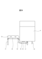
- Fig. 1 is a perspective view of a mounting structure including a short bar according to a first embodiment.
- a short bar S1 and a component P are mounted on the surface of a printed circuit board C.
- the component P may be a lead component having at least two leads L1, L2.
- the short bar S1 is an integral member made of a conductor, for example a conductive metal.
- the short bar S1 mainly includes two rising portions 11, 13 that rise relative to the surface of the printed circuit board C, a first extension portion 12 that connects the rising portions 11, 13 at a position spaced apart from the surface of the printed circuit board C, and a second extension portion 14 that extends from the rising portion 13 along the surface of the printed circuit board C.
- the base end of the rising portion 11 and the terminal end 16 of the second extension portion 14 extend to the back side through corresponding through holes in the printed circuit board C.
- the configuration of the short bar S1 is not limited to that shown in FIG. 1, and the short bar S1 only needs to include at least the rising portion 11 and the portion corresponding to the second extension portion 14.
- the second extension portion 14 has an engaged portion 15 that is to be engaged with the lead L1 of the component P.
- the engaged portion 15 shown in FIG. 1 can be a through hole formed in the second extension portion 14. It is preferable that the engaged portion 15 has a dimension that allows it to fit into the lead L1.
- the short bar S1 when a current is passed through the short bar S1 from the rising portion 11 side, the current passes through the first extension portion 12, the rising portion 13, and the second extension portion 14, and is transmitted to the lead L1 via the engaged portion 15. At this time, the current does not pass through the circuit pattern (not shown) on the back side of the printed circuit board C, so heat generation in the printed circuit board C is suppressed. Furthermore, the resistance value of the short bar S1 is lower than the resistance value of the circuit pattern (not shown) of the printed circuit board C. For this reason, even when a relatively large current is passed through the short bar S1, heat generation can be kept relatively small. The same is true for the component P.
- FIG. 2 is a perspective view of a mounting structure including a short bar based on the prior art.
- the prior art short bar S0 shown in FIG. 2 has two rising portions 11, 13 and a first extension portion 12 similar to those described above.
- the base ends of the rising portions 11, 13 extend to the rear surface side of the printed circuit board C as described above.
- the prior art short bar S0 does not have a second extension portion 14 equipped with an engaged portion 15.
- a large current can be transmitted from the rising portion 11 of the short bar S1 to the component P without passing through the circuit pattern of the printed circuit board C. This prevents the circuit pattern of the printed circuit board C itself from generating heat, and thus avoids the problems mentioned above.
- FIG. 3A is a perspective view of a short bar etc. based on the first embodiment.
- the engaged portion 15 of the short bar S1 and the lead L1 of the component P are engaged with each other as described above.
- FIG. 3B is a bottom view of FIG. 3A.
- the region including the engaged portion 15 and the lead L1 may be electrically connected by solder or solder flow.
- the structure of the short bar S1 can be simple, and the short bar S1 can be produced inexpensively.
- the base end of the rising portion 11 and the end portion 16 of the second extension portion 14 are soldered to a circuit pattern (not shown) formed on the back side of the printed circuit board C.
- a circuit pattern (not shown) formed on the back side of the printed circuit board C. The same is true for the leads L1 and L2 of the component P.
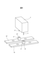
- FIG. 4 is a perspective view of a short bar based on the second embodiment.
- two short bars S2, S2' and a component P similar to that described above are shown.
- Sockets 21, 21' are provided on the short bars S2, S2', respectively.
- Holes 22, 22' that can be electrically connected to the short bars S2, S2' are formed on the sockets 21, 21'.
- component P when it becomes necessary to replace component P due to a malfunction or the like, component P can be easily removed by simply pulling out the leads L1, L2 of component P from the sockets 21, 21'. Furthermore, a new component P can be easily attached by simply inserting the leads L1, L2 of a new component P into the holes 22, 22' of the sockets 21, 21'.
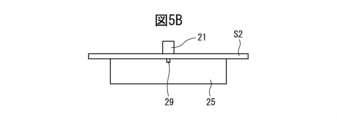
- FIGS. 5A to 5C are diagrams showing modified examples of the short bar shown in FIG. 4.
- through holes 24, 24' are formed in the positions of the short bars S2, S2' where the sockets 21, 21' should be provided.
- fasteners 23, 23' made of a conductor, such as screws or bolts are passed through the through holes 24, 24' of the short bars S2, S2' and screwed into the openings on the undersides of the sockets 21, 21'. This allows the sockets 21, 21' to be fixed to the short bars S2, S2', respectively.
- FIG. 5C one end of a rod 27, 27' made of a conductor is pressed into a through hole 26, 26' formed in the short bar S2, S2'.
- the other end of the rod 27, 27' is similarly pressed into a hole in the bottom surface of the socket 21, 21'.
- the configuration shown in FIG. 4 can be created by using any of FIG. 5A to FIG. 5C.
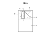
- FIGs. 6A and 6B are diagrams showing modified versions of the socket shown in Fig. 4 etc. Although these figures show socket 21, the same applies to socket 22.
- a hole 31 is formed in the top surface of socket 21 shown in Fig. 6A, and a plate portion 32 is provided in hole 31 that is rotatable around axis O perpendicular to the insertion direction of lead L1. Plate portion 32 is biased by leaf spring 33 in a direction that closes hole 31.
- lead L1 of component P when lead L1 of component P is inserted into hole 31, lead L1 presses against plate portion 32 against leaf spring 33.
- lead L1 In hole 31, lead L1 is sandwiched between the inner wall of hole 31 and plate portion 32.
- the inner wall of hole 31 is formed of a conductor.
- a through hole 34 is formed in the inner wall of the hole 31. Then, when the lead L1 of the component P is inserted into the hole 31, a fastener 35 made of a conductor is inserted into the through hole 34, and the lead L1 is pressed against an additional wall portion 38 or a leaf spring inside the hole 31 to fix it.
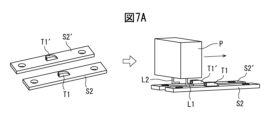
- FIGS. 7A to 7C are diagrams showing modified examples of the short bar shown in FIG. 4.
- tunnels T1 and T1' are formed in the short bars S2 and S2', respectively.
- Tunnels T1 and T1' are raised portions formed by raising a portion of the bottom surface of the short bars S2 and S2' toward the top surface, and at least one entrance is formed in the tunnels T1 and T1'.
- portions of the leads L1, L2 of component P are curved so as to be parallel to the surfaces of the short bars S2, S2'.
- the aforementioned portions of the leads L1, L2 are parallel to each other and extend in the same direction.
- the component P is slid along the surfaces of the short bars S2, S2', thereby inserting the leads L1, L2 into the tunnels T1, T1' from their entrances.
- the tunnels T1, T1' are pressed so as to crush them, thereby crimping the leads L1, L2 into the tunnels T1, T1', respectively.
- a portion of the leads L1, L2 of the component P is curved so as to be parallel to the surface of the short bars S2, S2'.
- the aforementioned portions of the leads L1, L2 extend in opposite directions on the same straight line.
- the ends 36, 36' of the short bars S2, S2' are at least partially curved upward.
- a through hole 37 is formed in the thickness portion of the short bar S2.
- the short bar S2' is formed in the thickness portion of the short bar S2.
- the tips of the curved leads L1 and L2 are inserted into the through holes 37 and 37' of the short bars S2 and S2', respectively.
- the surfaces of the short bars S2 and S2' corresponding to the through holes 37 and 37' are pressed to press the leads L1 and L2 into the through holes 37 and 37'.
- the leads L1, L2 and the short bars S2, S2' can be advantageously engaged without the need for additional parts, such as fasteners or adhesives, to electrically connect the leads L1, L2 and the short bars S2, S2'.
- FIGS. 8A and 8B are perspective views showing the mounting structure in the third embodiment
- FIG. 8C is a side view of FIG. 8B
- two short bars S3, S3' are mounted on the surface of the printed circuit board C.
- These short bars S3, S3' have engaged portions 15, 15', e.g. through holes, to be engaged with the leads L1, L2 of the component P, respectively.
- the component P has an additional lead L3 connected to the printed circuit board C.
- the leads L1 and L2 of the component P are engaged with the engaged portions 15 and 15' of the short bars S3 and S3', respectively. This causes the leads L1 and L2 to extend through the corresponding through holes formed in the printed circuit board C to the rear surface of the printed circuit board C.
- the back side of the printed circuit board C is processed with solder or solder flow 25.
- solder or solder flow 25 As a result, in the area shown by the dashed line in FIG. 8C, the leads L1 and L2, the short bars S3 and S3', and the printed circuit board C are electrically connected in a single process. Furthermore, in the same process, the lead L3 and the printed circuit board C are also electrically connected.
- leads L1, L2, short bars S3, S3', and printed circuit board C when processing lead L3, which requires soldering, leads L1, L2, short bars S3, S3', and printed circuit board C can also be processed simultaneously, reducing manufacturing man-hours. It can also be seen that in this process, lead L2, short bar S3', and printed circuit board C can also be processed simultaneously, further reducing manufacturing man-hours. Furthermore, in the third embodiment, it is not necessary to create separate electrical connection parts for short bars S3, S3' to printed circuit board C and electrical connection parts to component P. Therefore, it is also possible to miniaturize short bars S3, S3' and printed circuit board C.
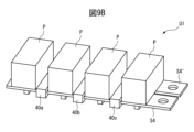
- FIGS. 9A and 9B are perspective views of a unit based on the fourth embodiment.
- the unit U1 shown in these figures includes at least two short bars S4, S4', a component P connected to the short bars S4, S4', and at least one insulating member 40a-40c that fixes the short bars S4, S4' in a spaced-apart state.
- Each of the short bars S4, S4' has at least one engaged portion 15. Therefore, as shown in FIG. 9B, at least one part P can be engaged therewith.
- the insulating members 40a to 40c are preferably made of a hard resin.
- the insulating members 40a to 40c can prevent the multiple short bars S4, S4' from shorting out with each other. Furthermore, the presence of the insulating members 40a to 40c can strengthen the engagement between the short bars S4, S4' and between the short bars S4, S4' and the leads L1, L2. This provides a unit U1 that is robust against external forces. Furthermore, the insulating members 40a to 40c also serve as positioning members that position the component P when it is mounted and when a servo amplifier (not shown) is attached.
- FIGS. 10A and 10B are diagrams showing a unit based on the fifth embodiment.
- Unit U2 includes a short bar S5 similar to that described above, and an insulating coating portion 41 that at least partially covers the surface of the short bar S5.
- the insulating coating portion 41 is preferably made of resin.
- the short bar S5 has at least one engaged portion 15.
- the insulating coating portion 41 has at least one notch 42 that generally corresponds to the at least one engaged portion 15.
- the insulating coating portion 43 is then moved laterally to attach the insulating coating portion 43 to the short bar S5.
- the insulating covering portion 41 insulates and covers the area of the short bar S5 other than at least one of the engaged portions 15.
- the insulating covering portion 41 may be configured to cover only one side of the short bar S5, or may be a bag-like structure that covers both sides of the short bar S5. *In this case, it can be attached by moving it laterally.
- the insulating coating portion 41 serves as an insulator between the short bar S5 and the component P (not shown in Figures 10A and 10B). Furthermore, by adjusting the thickness of the insulating coating portion 41, the insulating distance between the short bar S5 and the component P can be ensured.
- the insulating coating 41 fills the gap between the short bar S5 and the component P. Therefore, even if the short bar S5 is used in a machine (not shown) that vibrates a lot during use, the strength of the machine against vibrations can be increased.
- the unit U3 in the sixth embodiment mainly includes at least one short bar S6, S6' having an engaged portion 15, 15' (not shown in Figs. 11A and 11B) similar to that described above, an insulating coating portion 43, 43' similar to that described above that at least partially covers the surface of the short bar S6, S6', and a part P having a substantially rectangular parallelepiped shape.
- Each of the insulating coating parts 43, 43' has a positioning part 44, 44' that positions the component P. It is preferable that the insulating coating parts 43, 43' and the positioning parts 44, 44' are each formed integrally. Note that the insulating coating parts 43, 43' are attached to the short bars S6, S6', respectively, in the same manner as described with reference to Figures 10A and 10B.
- the component P when the leads L1, L2 of component P are to be engaged with the engaged portions 15, 15' of the short bars S6, S6', the component P is moved into the area formed by the two positioning portions 44, 44'. As described above, the positioning portions 44, 44' are provided at positions corresponding to the engaged portions 15, 15'. Therefore, by moving the component P so that the side portions of the component P slide along the walls of the positioning portions 44, 44', the leads L1, L2 of the component P can be easily engaged with the engaged portions 15, 15'.
- the positioning portions 44, 44' are provided in the insulating coating portions 43, 43' at positions corresponding to the engaged portions 15, 15'.
- the positioning portions 44, 44' include a wall portion that extends perpendicular to the insulating coating portions 43, 43'. It is preferable that the height of the wall portion is greater than half the height of the component P excluding the leads L1, L2.
- the positioning portions 44, 44' have a shape that corresponds to at least a portion of the side of the part P.
- the positioning portions 44, 44' can support at least a portion of the side of the part P, and therefore the vibration resistance of the unit U3 can be improved.
- the part P When the generally rectangular parallelepiped part P is viewed from above, the part P includes four corners.
- Each of the positioning portions 44, 44' shown in Figures 11A and 11B has a shape corresponding to two of the four corners.
- each of the positioning portions 44, 44' may have a shape corresponding to one of the four corners. In this case, it is preferable that the corner of the part P corresponding to the positioning portion 44 is not adjacent to the corner of the part P corresponding to the positioning portion 44'.
- each of the positioning portions 44, 44' may have a shape corresponding to half of the side of the component P.
- the positioning portions 44, 44' can cover the entire side of the component P, thereby improving the vibration resistance of the unit U3 and protecting the entire side of the component P.
- scope of this disclosure also includes cases where a single positioning portion 44 has a wall portion corresponding to the entire side of part P, and cases where a single positioning portion 44 has wall portions corresponding to three or more of the four corners of part P.
- the component P has leads L1, L2 that are longer than those described above.
- the positioning portions 44, 44' have spacers 48, 48' on the inside of their walls (spacers 48 are not shown).
- the spacers 48, 48' adjust the length of the leads L1, L2 so that only a portion of the tip of the leads L1, L2 engages with the corresponding engaged portion 15, 15'.
- the spacers 48, 48' are formed with slits 49, 49' through which the leads L1, L2 can pass (slits 49 are not shown).
- the bottom surface of the component P is seated on the upper end of the spacers 48, 48'. In such a case, even if the leads L1, L2 of the component P are long, only a portion of the tip of the leads L1, L2 can be engaged with the engaged portion 15, 15'.
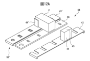
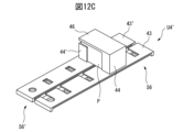
- FIGS. 12A to 12D are perspective views of a unit based on the seventh embodiment.
- the unit U4 in the seventh embodiment mainly includes at least one short bar S6, S6' having an engaged portion 15, 15' (not shown in FIG. 12A, etc.) similar to that described above, an insulating coating portion 43, 43' similar to that described above that at least partially covers the surface of the short bar S6, S6', and a part P having a substantially rectangular parallelepiped shape.
- Each of the insulating coating portions 43, 43' includes a positioning portion 44, 44' that positions the component P. Furthermore, at least one of the insulating coating portions 43 includes a closing portion 45 that at least partially closes the upper surface of the component P. As shown in FIG. 12A, the closing portion 45 is connected to the positioning portion 44. Therefore, it is preferable that the insulating coating portion 43, the positioning portion 44, and the closing portion 45 are integrally formed. Note that the height of the wall portion of the positioning portion 44 in the seventh embodiment is approximately equal to the height of the component P excluding the leads L1, L2.
- the insulating coating portion 43 which includes the positioning portion 44 and the closing portion 45, is moved laterally to attach the insulating coating portion 43 to the short bar S6. Since the insulating coating portion 43 has a notch 42 formed at a position corresponding to the engaged portion 15, the insulating coating portion 43 does not interfere with the lead L1 of the component P when it is attached. As a result, a portion of the component P is positioned in the space defined by the positioning portions 44, 44' and the closing portion 45. In this case, the side and part of the top surface of the component P are fixed, further improving vibration resistance.
- the effect of at least one of the embodiments described above is that the short bar and the lead of the lead component are directly engaged by the engaged portion. Since the resistance of the short bar is lower than that of the printed circuit board, heat generation in the short bar can be suppressed even when a large current is passed through it. Furthermore, there is no need to draw large patterns on the printed circuit board, which allows the printed circuit board to be made smaller. Also, since there is no need to increase the thickness of the copper foil on the printed circuit board, it is possible to reduce manufacturing costs.
- (Appendix 8) A plurality of short bars according to any one of appendices 1 to 4; and at least one insulating member that fixes the plurality of short bars in a spaced-apart state.
- (Appendix 9) A short bar according to any one of appendices 1 to 4; and an insulating covering portion that insulates and covers an area of the short bar other than the engaged portion.
- (Appendix 10) The unit described in claim 9, wherein the insulating coating portion includes a positioning portion that positions the lead component.
- the positioning portion further includes a closing portion that at least partially closes an upper surface of the lead component.
- (Appendix 12) 11 The unit of claim 10, wherein the closure portion has an additional positioning portion formed therein.
Landscapes
- Engineering & Computer Science (AREA)
- Microelectronics & Electronic Packaging (AREA)
- Coupling Device And Connection With Printed Circuit (AREA)
- Structures For Mounting Electric Components On Printed Circuit Boards (AREA)
Abstract
Description
図1は第一の実施形態に基づくショートバーを含む実装構造部の斜視図である。図1においては、プリント基板Cの表面に、少なくとも一つのショートバーS1と部品Pとが実装されている。部品Pは少なくとも二つのリードL1、L2を備えたリード部品でありうる。
(付記1)
リード部品に電気的に接続されるショートバーにおいて、
前記リード部品のリードに係合されるべき被係合部を備えたショートバー。
(付記2)
前記被係合部は前記リード部品の前記リードを受容するソケットである、付記1に記載のショートバー。
(付記3)
前記被係合部は前記リード部品の前記リードを圧着する圧着部分である、付記1に記載のショートバー。
(付記4)
前記リードと前記被係合部とが半田または半田フローにより電気的に接続される、付記1または2に記載のショートバー。
(付記5)
プリント基板と、
該プリント基板に実装されていて付記1に記載のショートバーと、を含んでおり、
前記ショートバーの前記被係合部に係合する前記リード部品の前記リードは前記ショートバーを越えて前記プリント基板の貫通孔を貫通するようにした、実装構造部。
(付記6)
前記リードと前記被係合部とが半田または半田フローにより電気的に接続される、付記5に記載の実装構造部。
(付記7)
付記1から4のいずれかに記載のショートバーと、
該ショートバーに実装されたプリント基板とを含んでおり、
前記リード部品の前記リードは前記プリント基板の貫通孔を貫通して前記ショートバーの前記被係合部に係合するようにした、実装構造部。
(付記8)
付記1から4のいずれかに記載される複数のショートバーと、
該複数のショートバーを互いに離間した状態で固定する少なくとも一つの絶縁部材とを含む、ユニット。
(付記9)
付記1から4のいずれかに記載されるショートバーと、
該ショートバーの前記被係合部以外の領域を絶縁して被覆する絶縁被覆部とを含む、ユニット。
(付記10)
前記絶縁被覆部は、前記リード部品を位置決めする位置決め部を含む、付記9に記載のユニット。
(付記11)
前記位置決め部は、さらに、前記リード部品の上面を少なくとも部分的に閉鎖する閉鎖部を含む、付記10に記載のユニット。
(付記12)
前記閉鎖部には、追加位置決め部が形成されている、付記10に記載のユニット。
12 第一延長部
14 第二延長部
15、15’ 被係合部
21、21’ ソケット
22、22’ 孔
24、24’ 貫通孔
25 半田フロー
27、27’ 棒体
32 板部
33 板バネ
35 留め具
36、36’ 端部
37、37’ 貫通孔
38 追加壁部、板バネ
40a~40c 絶縁部材
41 絶縁被覆部
42 切欠
43、43’ 絶縁被覆部
44、44’ 位置決め部
45、46 閉鎖部
47 追加位置決め部
48、48’ スペーサ
49、49’ スリット
C プリント基板
L1、L2 リード
P 部品
S1、S2、S2’、S3、S3’、S4、S4’、S5、S6、S6’ ショートバー
T1、T1’ トンネル
U1、U2、U3、U3’、U4、U4’ ユニット
Claims (12)
- リード部品に電気的に接続されるショートバーにおいて、
前記リード部品のリードに係合されるべき被係合部を備えたショートバー。 - 前記被係合部は前記リード部品の前記リードを受容するソケットである、請求項1に記載のショートバー。
- 前記被係合部は前記リード部品の前記リードを圧着する圧着部分である、請求項1に記載のショートバー。
- 前記リードと前記被係合部とが半田または半田フローにより電気的に接続される、請求項1に記載のショートバー。
- プリント基板と、
該プリント基板に実装されていて請求項1に記載のショートバーと、を含んでおり、
前記ショートバーの前記被係合部に係合する前記リード部品の前記リードは前記ショートバーを越えて前記プリント基板の貫通孔を貫通するようにした、実装構造部。 - 前記リードと前記被係合部とが半田または半田フローにより電気的に接続される、請求項5に記載の実装構造部。
- 請求項1に記載のショートバーと、
該ショートバーに実装されたプリント基板とを含んでおり、
前記リード部品の前記リードは前記プリント基板の貫通孔を貫通して前記ショートバーの前記被係合部に係合するようにした、実装構造部。 - 請求項1に記載される複数のショートバーと、
該複数のショートバーを互いに離間した状態で固定する少なくとも一つの絶縁部材とを含む、ユニット。 - 請求項1に記載されるショートバーと、
該ショートバーの前記被係合部以外の領域を絶縁して被覆する絶縁被覆部とを含む、ユニット。 - 前記絶縁被覆部は、前記リード部品を位置決めする位置決め部を含む、請求項9に記載のユニット。
- 前記位置決め部は、さらに、前記リード部品の上面を少なくとも部分的に閉鎖する閉鎖部を含む、請求項10に記載のユニット。
- 前記閉鎖部には、追加位置決め部が形成されている、請求項10に記載のユニット。
Priority Applications (5)
| Application Number | Priority Date | Filing Date | Title |
|---|---|---|---|
| CN202380095694.9A CN120858654A (zh) | 2023-03-29 | 2023-03-29 | 短路棒、安装构造部以及单元 |
| DE112023005637.4T DE112023005637T5 (de) | 2023-03-29 | 2023-03-29 | Kurzschlussleiste, befestigungsstruktur und einheit |
| JP2025509446A JPWO2024201833A1 (ja) | 2023-03-29 | 2023-03-29 | |
| PCT/JP2023/012940 WO2024201833A1 (ja) | 2023-03-29 | 2023-03-29 | ショートバー、実装構造部およびユニット |
| US19/195,113 US20250260186A1 (en) | 2023-03-29 | 2025-04-30 | Shorting bar, mounting structure, and unit |
Applications Claiming Priority (1)
| Application Number | Priority Date | Filing Date | Title |
|---|---|---|---|
| PCT/JP2023/012940 WO2024201833A1 (ja) | 2023-03-29 | 2023-03-29 | ショートバー、実装構造部およびユニット |
Related Child Applications (1)
| Application Number | Title | Priority Date | Filing Date |
|---|---|---|---|
| US19/195,113 Continuation US20250260186A1 (en) | 2023-03-29 | 2025-04-30 | Shorting bar, mounting structure, and unit |
Publications (1)
| Publication Number | Publication Date |
|---|---|
| WO2024201833A1 true WO2024201833A1 (ja) | 2024-10-03 |
Family
ID=92903651
Family Applications (1)
| Application Number | Title | Priority Date | Filing Date |
|---|---|---|---|
| PCT/JP2023/012940 Ceased WO2024201833A1 (ja) | 2023-03-29 | 2023-03-29 | ショートバー、実装構造部およびユニット |
Country Status (5)
| Country | Link |
|---|---|
| US (1) | US20250260186A1 (ja) |
| JP (1) | JPWO2024201833A1 (ja) |
| CN (1) | CN120858654A (ja) |
| DE (1) | DE112023005637T5 (ja) |
| WO (1) | WO2024201833A1 (ja) |
Citations (7)
| Publication number | Priority date | Publication date | Assignee | Title |
|---|---|---|---|---|
| JPH0245666U (ja) * | 1988-09-22 | 1990-03-29 | ||
| JP2000232281A (ja) * | 1999-02-09 | 2000-08-22 | Matsushita Electric Ind Co Ltd | 成形回路基板及び部品保持具 |
| JP2001035562A (ja) * | 1999-07-07 | 2001-02-09 | Molex Inc | 3dモールド回路板 |
| JP2006173427A (ja) * | 2004-12-17 | 2006-06-29 | Union Machinery Co Ltd | 打ち抜き金属板製のバスバーへの電気素子の圧着固定方法。 |
| JP2008048516A (ja) * | 2006-08-11 | 2008-02-28 | Sumitomo Wiring Syst Ltd | 電気接続箱に収容する回路材および該回路材を収容する車載用の電気接続箱 |
| JP2020181929A (ja) * | 2019-04-26 | 2020-11-05 | 住友電装株式会社 | 基板、部品実装基板、電気接続箱及び基板の製造方法 |
| CN212381599U (zh) * | 2020-07-07 | 2021-01-19 | 锦浪科技股份有限公司 | 一种基于汇流条的散热系统 |
-
2023
- 2023-03-29 WO PCT/JP2023/012940 patent/WO2024201833A1/ja not_active Ceased
- 2023-03-29 DE DE112023005637.4T patent/DE112023005637T5/de active Pending
- 2023-03-29 JP JP2025509446A patent/JPWO2024201833A1/ja active Pending
- 2023-03-29 CN CN202380095694.9A patent/CN120858654A/zh active Pending
-
2025
- 2025-04-30 US US19/195,113 patent/US20250260186A1/en active Pending
Patent Citations (7)
| Publication number | Priority date | Publication date | Assignee | Title |
|---|---|---|---|---|
| JPH0245666U (ja) * | 1988-09-22 | 1990-03-29 | ||
| JP2000232281A (ja) * | 1999-02-09 | 2000-08-22 | Matsushita Electric Ind Co Ltd | 成形回路基板及び部品保持具 |
| JP2001035562A (ja) * | 1999-07-07 | 2001-02-09 | Molex Inc | 3dモールド回路板 |
| JP2006173427A (ja) * | 2004-12-17 | 2006-06-29 | Union Machinery Co Ltd | 打ち抜き金属板製のバスバーへの電気素子の圧着固定方法。 |
| JP2008048516A (ja) * | 2006-08-11 | 2008-02-28 | Sumitomo Wiring Syst Ltd | 電気接続箱に収容する回路材および該回路材を収容する車載用の電気接続箱 |
| JP2020181929A (ja) * | 2019-04-26 | 2020-11-05 | 住友電装株式会社 | 基板、部品実装基板、電気接続箱及び基板の製造方法 |
| CN212381599U (zh) * | 2020-07-07 | 2021-01-19 | 锦浪科技股份有限公司 | 一种基于汇流条的散热系统 |
Also Published As
| Publication number | Publication date |
|---|---|
| JPWO2024201833A1 (ja) | 2024-10-03 |
| US20250260186A1 (en) | 2025-08-14 |
| CN120858654A (zh) | 2025-10-28 |
| DE112023005637T5 (de) | 2025-11-20 |
Similar Documents
| Publication | Publication Date | Title |
|---|---|---|
| CN102334389B (zh) | 连接单元 | |
| JP2010087044A (ja) | 電子機器 | |
| JP6330690B2 (ja) | 基板ユニット | |
| JP2017098332A (ja) | 電子回路装置 | |
| WO2024201833A1 (ja) | ショートバー、実装構造部およびユニット | |
| JP2010086071A (ja) | 電子機器 | |
| JP2018137267A (ja) | 電子部品 | |
| JP3870769B2 (ja) | コネクタ搭載構造 | |
| JP2021061700A (ja) | 電気接続箱 | |
| JP2008125190A (ja) | 電気接続箱 | |
| JP2011181468A (ja) | バスバー付基板用端子 | |
| JP5080326B2 (ja) | 電子部品の端子接続構造及び電動パワーステアリング装置のコントロールユニット構造並びに電子部品の端子接続方法 | |
| JP6986380B2 (ja) | コネクタの取付構造およびコネクタシールド | |
| CN111567154A (zh) | 汇流条以及汇流条固定结构 | |
| JP5381617B2 (ja) | 電気接続箱 | |
| JP4760097B2 (ja) | キャパシタバンク用電極板及びキャパシタバンク | |
| JP4869419B2 (ja) | 電子機器 | |
| JP4692085B2 (ja) | 電子部品 | |
| JP3610493B2 (ja) | ジャンパ線の配線構造 | |
| JP7294386B2 (ja) | バスバー位置決め構造及び電気機器 | |
| JP5973342B2 (ja) | 回路基板と接続端子の接続構造 | |
| JP2002208794A (ja) | 電磁波障害防止用部品 | |
| JP5397196B2 (ja) | 基板端子用台座 | |
| JP6010819B2 (ja) | コネクタの基板固定構造 | |
| JP2011182611A (ja) | 接続端子付きプリント基板 |
Legal Events
| Date | Code | Title | Description |
|---|---|---|---|
| 121 | Ep: the epo has been informed by wipo that ep was designated in this application |
Ref document number: 23930471 Country of ref document: EP Kind code of ref document: A1 |
|
| WWE | Wipo information: entry into national phase |
Ref document number: 2025509446 Country of ref document: JP |
|
| WWE | Wipo information: entry into national phase |
Ref document number: 202380095694.9 Country of ref document: CN |
|
| WWE | Wipo information: entry into national phase |
Ref document number: 112023005637 Country of ref document: DE |
|
| WWP | Wipo information: published in national office |
Ref document number: 202380095694.9 Country of ref document: CN |
|
| 122 | Ep: pct application non-entry in european phase |
Ref document number: 23930471 Country of ref document: EP Kind code of ref document: A1 |