WO2024195468A1 - 電子部品および電子部品の製造方法 - Google Patents
電子部品および電子部品の製造方法 Download PDFInfo
- Publication number
- WO2024195468A1 WO2024195468A1 PCT/JP2024/007527 JP2024007527W WO2024195468A1 WO 2024195468 A1 WO2024195468 A1 WO 2024195468A1 JP 2024007527 W JP2024007527 W JP 2024007527W WO 2024195468 A1 WO2024195468 A1 WO 2024195468A1
- Authority
- WO
- WIPO (PCT)
- Prior art keywords
- seed layer
- insulating
- layer
- wiring
- electronic component
- Prior art date
- Legal status (The legal status is an assumption and is not a legal conclusion. Google has not performed a legal analysis and makes no representation as to the accuracy of the status listed.)
- Ceased
Links
Images













Classifications
-
- H—ELECTRICITY
- H05—ELECTRIC TECHNIQUES NOT OTHERWISE PROVIDED FOR
- H05K—PRINTED CIRCUITS; CASINGS OR CONSTRUCTIONAL DETAILS OF ELECTRIC APPARATUS; MANUFACTURE OF ASSEMBLAGES OF ELECTRICAL COMPONENTS
- H05K3/00—Apparatus or processes for manufacturing printed circuits
- H05K3/10—Apparatus or processes for manufacturing printed circuits in which conductive material is applied to the insulating support in such a manner as to form the desired conductive pattern
- H05K3/18—Apparatus or processes for manufacturing printed circuits in which conductive material is applied to the insulating support in such a manner as to form the desired conductive pattern using precipitation techniques to apply the conductive material
-
- H—ELECTRICITY
- H05—ELECTRIC TECHNIQUES NOT OTHERWISE PROVIDED FOR
- H05K—PRINTED CIRCUITS; CASINGS OR CONSTRUCTIONAL DETAILS OF ELECTRIC APPARATUS; MANUFACTURE OF ASSEMBLAGES OF ELECTRICAL COMPONENTS
- H05K3/00—Apparatus or processes for manufacturing printed circuits
- H05K3/46—Manufacturing multilayer circuits
-
- H—ELECTRICITY
- H10—SEMICONDUCTOR DEVICES; ELECTRIC SOLID-STATE DEVICES NOT OTHERWISE PROVIDED FOR
- H10W—GENERIC PACKAGES, INTERCONNECTIONS, CONNECTORS OR OTHER CONSTRUCTIONAL DETAILS OF DEVICES COVERED BY CLASS H10
- H10W70/00—Package substrates; Interposers; Redistribution layers [RDL]
- H10W70/60—Insulating or insulated package substrates; Interposers; Redistribution layers
Definitions
- This disclosure relates to electronic components and methods for manufacturing electronic components.
- the redistribution layer is formed using a method such as plating. For example, when forming the redistribution layer using electroless plating, it is necessary to form a seed layer made of a conductor using sputtering or the like on an insulating layer made of resin or the like. This makes manufacturing complicated.
- An object of the present disclosure is to provide electronic components and methods for manufacturing electronic components that are improved over conventional ones.
- an object of the present disclosure is to provide electronic components and methods for manufacturing electronic components that can be manufactured more easily.
- the electronic component provided by the first aspect of the present disclosure includes a first functional element, a first insulating seed layer laminated on one side in the thickness direction of the first functional element, and a first wiring layer laminated on the one side in the thickness direction of the first insulating seed layer.
- the above configuration makes it possible to provide electronic components that can be manufactured more easily and a method for manufacturing electronic components.
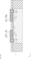
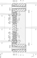
- FIG. 1 is a plan view showing an electronic component according to a first embodiment of the present disclosure.
- FIG. 2 is a cross-sectional view taken along line II-II in FIG.
- FIG. 3 is a cross-sectional view showing an example of a method for manufacturing an electronic component according to the first embodiment of the present disclosure.
- FIG. 4 is a cross-sectional view showing an example of a method for manufacturing an electronic component according to the first embodiment of the present disclosure.
- FIG. 5 is a cross-sectional view showing an example of a method for manufacturing an electronic component according to the first embodiment of the present disclosure.
- FIG. 6 is a cross-sectional view showing an example of a method for manufacturing an electronic component according to the first embodiment of the present disclosure.
- FIG. 1 is a plan view showing an electronic component according to a first embodiment of the present disclosure.
- FIG. 2 is a cross-sectional view taken along line II-II in FIG.
- FIG. 3 is a cross-sectional view showing an example of a method
- FIG. 7 is a cross-sectional view showing an example of a method for manufacturing an electronic component according to the first embodiment of the present disclosure.
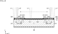
- FIG. 8 is a cross-sectional view showing an example of a method for manufacturing an electronic component according to the first embodiment of the present disclosure.
- FIG. 9 is a partially enlarged cross-sectional view showing a first modified example of the electronic component according to the first embodiment of the present disclosure.
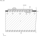
- FIG. 10 is a partially enlarged cross-sectional view showing a manufacturing method for a first modified example of the electronic component according to the first embodiment of the present disclosure.
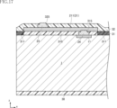
- FIG. 11 is a partially enlarged cross-sectional view showing a manufacturing method for a first modified example of the electronic component according to the first embodiment of the present disclosure.
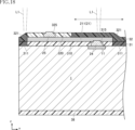
- FIG. 12 is a partially enlarged cross-sectional view showing a manufacturing method for a first modified example of the electronic component according to the first embodiment of the present disclosure.
- FIG. 13 is a partially enlarged cross-sectional view showing a manufacturing method for a first modified example of the electronic component according to the first embodiment of the present disclosure.
- FIG. 14 is a partially enlarged cross-sectional view showing a manufacturing method for a first modified example of the electronic component according to the first embodiment of the present disclosure.
- FIG. 15 is a partially enlarged cross-sectional view showing a manufacturing method for a first modified example of the electronic component according to the first embodiment of the present disclosure.
- FIG. 16 is a partially enlarged cross-sectional view showing a manufacturing method for a first modified example of the electronic component according to the first embodiment of the present disclosure.
- FIG. 17 is a partially enlarged cross-sectional view showing a manufacturing method for a first modified example of the electronic component according to the first embodiment of the present disclosure.
- FIG. 18 is a partially enlarged cross-sectional view showing a manufacturing method for a first modified example of the electronic component according to the first embodiment of the present disclosure.
- FIG. 19 is a cross-sectional view showing a second modified example of the electronic component according to the first embodiment of the present disclosure.
- FIG. 20 is a plan view showing an electronic component according to a second embodiment of the present disclosure.
- FIG. 21 is a cross-sectional view taken along line XXI-XXI in FIG.
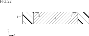
- FIG. 22 is a cross-sectional view showing an example of a method for manufacturing an electronic component according to the second embodiment of the present disclosure.
- FIG. 23 is a cross-sectional view showing an example of a method for manufacturing an electronic component according to the second embodiment of the present disclosure.
- FIG. 24 is a cross-sectional view showing an example of a method for manufacturing an electronic component according to the second embodiment of the present disclosure.
- FIG. 25 is a cross-sectional view showing an example of a method for manufacturing an electronic component according to the second embodiment of the present disclosure.
- FIG. 26 is a cross-sectional view showing an example of a method for manufacturing an electronic component according to the second embodiment of the present disclosure.
- FIG. 27 is a partially enlarged cross-sectional view showing a specific example of an electronic component according to a second embodiment of the present disclosure.
- FIG. 28 is a partially enlarged cross-sectional view showing another specific example of the electronic component according to the second embodiment of the present disclosure.
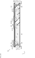
- FIG. 29 is a cross-sectional view showing a first modified example of the electronic component according to the second embodiment of the present disclosure.
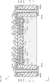
- FIG. 30 is a cross-sectional view showing an electronic component according to a third embodiment of the present disclosure.
- FIG. 31 is a cross-sectional view showing an example of a method for manufacturing an electronic component according to the third embodiment of the present disclosure.
- FIG. 32 is a cross-sectional view showing an example of a method for manufacturing an electronic component according to the third embodiment of the present disclosure.
- FIG. 33 is a cross-sectional view showing an example of a method for manufacturing an electronic component according to the third embodiment of the present disclosure.
- FIG. 34 is a cross-sectional view showing an example of a method for manufacturing an electronic component according to the third embodiment of the present disclosure.
- FIG. 35 is a cross-sectional view showing an example of a method for manufacturing an electronic component according to the third embodiment of the present disclosure.
- FIG. 36 is a cross-sectional view showing an example of a method for manufacturing an electronic component according to the third embodiment of the present disclosure.
- FIG. 37 is a cross-sectional view showing an example of a method for manufacturing an electronic component according to the third embodiment of the present disclosure.
- FIG. 38 is a cross-sectional view showing an example of a method for manufacturing an electronic component according to the third embodiment of the present disclosure.
- FIG. 39 is a cross-sectional view showing an example of a method for manufacturing an electronic component according to the third embodiment of the present disclosure.
- FIG. 40 is a cross-sectional view showing an example of a method for manufacturing an electronic component according to the third embodiment of the present disclosure.
- FIG. 41 is a cross-sectional view showing an example of a method for manufacturing an electronic component according to the third embodiment of the present disclosure.
- FIG. 42 is a cross-sectional view showing an example of a method for manufacturing an electronic component according to the third embodiment of the present disclosure.
- FIG. 43 is a cross-sectional view showing an example of a method for manufacturing an electronic component according to the third embodiment of the present disclosure.
- FIG. 44 is a cross-sectional view showing an example of a method for manufacturing an electronic component according to the third embodiment of the present disclosure.
- FIG. 45 is a cross-sectional view showing an example of a method for manufacturing an electronic component according to the third embodiment of the present disclosure.
- an object A is formed on an object B" and “an object A is formed on an object B” include “an object A is formed directly on an object B” and “an object A is formed on an object B with another object interposed between the object A and the object B” unless otherwise specified.
- an object A is disposed on an object B” and “an object A is disposed on an object B” include “an object A is disposed directly on an object B” and “an object A is disposed on an object B with another object interposed between the object A and the object B" unless otherwise specified.
- an object A is located on an object B includes “an object A is located on an object B in contact with an object B” and “an object A is located on an object B with another object interposed between the object A and the object B” unless otherwise specified.
- an object A overlaps an object B when viewed in a certain direction includes “an object A overlaps the entire object B” and “an object A overlaps a part of an object B.”
- a surface A faces in direction B is not limited to the case where the angle of surface A with respect to direction B is 90 degrees, but also includes the case where surface A is tilted with respect to direction B.
- First embodiment: 1 and 2 show an electronic component according to a first embodiment of the present disclosure.
- the electronic component A1 of this embodiment includes a first functional element 1, a first wiring layer 21, a second wiring layer 22, a first insulating seed layer 31, a second insulating seed layer 32, and a back surface insulating seed layer 38.
- the electronic component A1 is mounted on, for example, a circuit board (not shown) using the second wiring layer 22.
- the use and specific functions of the electronic component A1 are not limited in any way.
- the z direction is an example of the "thickness direction.”
- An example of a direction perpendicular to the z direction is defined as the x direction.
- the direction perpendicular to the z direction and the x direction is defined as the y direction.
- the first functional element 1 is an element that performs the main electronic function of the electronic component A1.
- the specific configuration of the first functional element 1 is not limited in any way.
- Examples of the first functional element 1 include semiconductor elements and various passive elements. Examples of the semiconductor elements include LSIs (Large Scale Integration) and ICs (Integrated Circuits). Examples of the passive elements include inductors.
- the first functional element 1 of this embodiment has a plurality of electrodes 11.
- the plurality of electrodes 11 are for electrically connecting the first functional element 1 to the outside.
- the electrodes 11 include metals such as Cu (copper), Al (aluminum), Au (gold), Ni (nickel), etc., and alloys thereof.
- the electrodes 11 may also be formed with a plating layer or the like (not shown). In the illustrated example, the plurality of electrodes 11 are arranged on one side of the first functional element 1 in the z direction.
- First insulating seed layer 31, second insulating seed layer 32, back insulating seed layer 38 The first insulating seed layer 31, the second insulating seed layer 32, and the back insulating seed layer 38 are laminated together with the first functional element 1. They are layers that function as seed layers for electroless plating to form the first insulating seed layer 31, the second insulating seed layer 32, and the back insulating seed layer 38, and have insulating properties. Specific examples of the first insulating seed layer 31, the second insulating seed layer 32, and the back insulating seed layer 38 are not limited in any way, and for example, a plating primer "Metalloid" (registered trademark) manufactured by IOX Corporation can be used as an example.
- a plating primer "Metalloid" registered trademark
- the thicknesses of the first insulating seed layer 31, the second insulating seed layer 32, and the back insulating seed layer 38 are not limited in any way. Specific examples of the thicknesses of the first insulating seed layer 31, the second insulating seed layer 32, and the back insulating seed layer 38 are, for example, 50 nm or more and 3000 nm or less, for example, about 270 nm.
- the first insulating seed layer 31 is laminated on one side in the z direction relative to the first functional element 1.
- the second insulating seed layer 32 is laminated on one side in the z direction relative to the first insulating seed layer 31.
- the back surface insulating seed layer 38 is laminated on the other side in the z direction relative to the first functional element 1. Note that the electronic component according to the present disclosure may be configured without the second insulating seed layer 32 and the back surface insulating seed layer 38.
- the first insulating seed layer 31 includes a first activated region 310 and a first inactivated region 311.
- the first activated region 310 is a region that functions as a seed layer for forming electroless plating.
- the first inactivated region 311 is a region in which the function as a seed layer for forming electroless plating is inactivated.
- the first insulating seed layer 31 has a plurality of through holes 315.
- the through holes 315 penetrate the first insulating seed layer 31 in the z direction.
- the through holes 315 are provided in the first activated region 310. Furthermore, the plurality of through holes 315 individually overlap with the plurality of electrodes 11 when viewed in the z direction.
- the second insulating seed layer 32 includes a second activated region 320 and a second inactivated region 321.
- the second activated region 320 is a region that functions as a seed layer for forming electroless plating, or electroless plating and electroplating.
- the second inactivated region 321 is a region in which the function as a seed layer for forming electroless plating, or electroless plating and electroplating, is inactivated.
- the second insulating seed layer 32 has a through hole 325.
- the through hole 325 penetrates the second insulating seed layer 32 in the z-direction.
- the through hole 325 is provided in the second activated region 320.
- First wiring layer 21, second wiring layer 22, first through wiring section 24, second through wiring section 25 The first wiring layer 21, the second wiring layer 22, the first through wiring portion 24, and the second through wiring portion 25 form a conductive path for realizing the function of the electronic component A1.
- the materials of the second wiring layer 22, the first through wiring portion 24 and the second through wiring portion 25 are not limited in any way, and are preferably, for example, a material containing Cu (copper) or a Cu (copper) alloy.
- the first wiring layer 21 includes a plurality of first wiring portions 211.
- the plurality of first wiring portions 211 are separated from each other when viewed in the z direction.
- the plurality of first wiring portions 211 overlap with the plurality of electrodes 11 individually when viewed in the z direction.
- the plurality of first wiring portions 211 overlap with the plurality of through holes 315 individually when viewed in the z direction.
- the second wiring layer 22 is laminated on one side of the second insulating seed layer 32 in the z direction.
- the second wiring layer 22 is located between the second insulating seed layer 32 and the second insulating seed layer 32.
- the second wiring layer 22 is in direct contact with the second insulating seed layer 32.
- the second wiring layer 22 is in direct contact with the second insulating seed layer 32.
- No seed layer made of a metal such as Ti (titanium) is provided between the second wiring layer 22 and the second insulating seed layer 32.
- the thickness of the second wiring layer 22 is not limited in any way, and is specifically 100 nm or more and 4000 nm or less, for example, about 270 nm.
- the second wiring layer 22 includes a plurality of terminal portions 222.
- the terminal portions 222 are separated from each other when viewed in the z direction. When viewed in the z direction, the plurality of terminal portions 222 overlap with the plurality of through holes 325 individually.
- the plurality of terminal portions 222 are used, for example, to mount the electronic component A1 on a circuit board (not shown) or the like.
- the surface of the terminal portion 222 may be provided with a plating layer (not shown) that improves the wettability of the solder, or may be provided with a solder ball (not shown).
- the multiple first through wiring parts 24 penetrate the first insulating seed layer 31 in the z-direction.
- the multiple first through wiring parts 24 are individually housed in multiple through holes 315.
- the multiple first through wiring parts 24 are in direct contact with the first insulating seed layer 31.
- No seed layer made of a metal such as Ti (titanium) is provided between the multiple first through wiring parts 24 and the first insulating seed layer 31.
- the multiple first through wiring parts 24 are individually connected to the multiple electrodes 11 and the multiple first wiring parts 211, and individually conduct the multiple electrodes 11 and the multiple first wiring parts 211.
- the second through wiring portions 25 penetrate the second insulating seed layer 32 in the z-direction.
- the second through wiring portions 25 are individually housed in the through holes 325.
- the second through wiring portions 25 are in direct contact with the second insulating seed layer 32.
- No seed layer made of a metal such as Ti (titanium) is provided between the second through wiring portions 25 and the second insulating seed layer 32.
- the second through wiring portions 25 are individually connected to the first wiring portions 211 and the terminal portions 222, and individually conduct the first wiring portions 211 and the terminal portions 222.
- the first insulating seed layer 31 and the back insulating seed layer 38 are laminated.
- This step is performed, for example, by applying a liquid material, which is the material of the first insulating seed layer 31 and the back insulating seed layer 38, to the first functional element 1.
- a liquid material which is the material of the first insulating seed layer 31 and the back insulating seed layer 38
- the liquid material is applied from one side and the other side of the first functional element 1 in the z direction, so that the liquid material adheres to both sides of the first functional element 1.
- the first insulating seed layer 31 and the back insulating seed layer 38 are obtained by appropriately hardening this liquid material.
- There are no specific limitations on the specific method for applying the liquid material and various methods such as spraying, spin coating, bar coating, dipping, and inkjet printing can be used.
- the first insulating seed layer 31 is irradiated with laser light L1 and laser light L2.
- the region irradiated with laser light L1 is a region of the first insulating seed layer 31 where the first wiring layer 21 is not formed (first activation region 310).
- the irradiation with laser light L1 is performed on a region that avoids the region where the first wiring layer 21 is formed.
- a first inactivation region 311 is formed in the first insulating seed layer 31 by the irradiation with laser light L1.
- the region of the first insulating seed layer 31 where the laser light L1 is not irradiated is the first activation region 310.
- the laser light L1 is irradiated in such a manner that the function of the first insulating seed layer 31 as a seed layer is inactivated by irradiating the laser light L1.
- the position where the laser light L2 is irradiated is the position where a plurality of through holes 315 should be formed.
- a plurality of through holes 315 are formed in the first insulating seed layer 31.
- the laser light L2 is irradiated in such a manner that the through holes 315 are formed in the first insulating seed layer 31 by irradiating the laser light L2.
- Laser light L2 is a laser light with a wavelength, output, irradiation time, etc. that can penetrate the first insulating seed layer 31.
- Laser light L1 and laser light L2 may be irradiated using different laser devices. Alternatively, the same laser device may be used to irradiate laser light L1 and laser light L2 by appropriately adjusting the wavelength, output, irradiation time, etc.
- the first wiring layer 21 and the multiple first through wiring parts 24 are formed.
- the first wiring layer 21 and the multiple first through wiring parts 24 are formed by electroless plating, or electroless plating and electroplating, using the first activation region 310 of the first insulating seed layer 31 as a seed layer.
- a plating layer containing, for example, Cu (copper) or a Cu (copper) alloy grows on the first activation region 310.
- This plating layer becomes the first wiring layer 21 and the multiple first through wiring parts 24.
- no plating layer grows on the first inactivated region 311 because its function as a seed layer is inactivated.
- the first wiring layer 21 is formed by growing a plating layer on one surface of the first activation region 310 in the z direction.
- a plurality of first wiring parts 211 are formed corresponding to the plurality of first activation regions 310.
- the plurality of first through wiring parts 24 are formed, for example, by growing a plating layer on the inner surface of a plurality of through holes 315. Also, a portion of each of the plurality of first through wiring parts 24 may be formed by growing a plating layer on the surfaces of a plurality of electrodes 11. According to the manufacturing method of the illustrated example, the first wiring part 211 and the first through wiring part 24 are formed integrally.
- the second insulating seed layer 32 is laminated.
- the second insulating seed layer 32 is formed, for example, in the same manner as the formation of the first insulating seed layer 31 and the back surface insulating seed layer 38, by applying a liquid material and then curing the applied liquid material.
- the second insulating seed layer 32 is irradiated with laser light L1 and laser light L2.
- the area of the second insulating seed layer 32 irradiated with the laser light L1 becomes the second inactivated area 321, and the area not irradiated with the laser light L1 becomes the second activated area 320.
- a plurality of through holes 325 are formed in the third wiring layer 23.
- electroless plating or electroless plating and electroplating are performed using the second activation region 320 of the second insulating seed layer 32 as a seed layer to form the second wiring layer 22 and the multiple second through wiring portions 25 shown in FIG. 2.
- the second wiring layer 22 is formed by growing a plating layer on one surface of the second activation region 320 in the z direction.
- a plurality of terminal portions 222 are formed corresponding to the plurality of second activation regions 320.
- the plurality of second through wiring portions 25 are formed, for example, by growing a plating layer on the inner surface of a plurality of through holes 325. Also, a portion of each of the plurality of second through wiring portions 25 may be formed by growing a plating layer on the surface of a portion of the plurality of first wiring portions 211 surrounded by the through holes 325. According to the manufacturing method of the illustrated example, the terminal portion 222 and the second through wiring portion 25 are formed integrally. Through the above steps, the electronic component A1 is obtained.
- a first insulating seed layer 31 is interposed between the first functional element 1 and the first wiring layer 21.
- the first insulating seed layer 31 has insulating properties and can properly insulate the first functional element 1 from the first wiring layer 21.
- the first wiring layer 21 is also laminated on the first insulating seed layer 31.
- the first activation region 310 functions as a seed layer in electroless plating. For this reason, there is no need to form a dedicated seed layer for forming the first wiring layer 21. This makes it easier to manufacture the electronic component A1.
- a first inactivated region 311 is formed in the first insulating seed layer 31.
- the first inactivated region 311 by irradiating the laser light L1, it is possible to form the first wiring layer 21 in a finer and more accurate shape.
- no through holes are formed in the first insulating seed layer 31 by inactivation with the laser light L1. Therefore, it is possible to maintain the function of the first insulating seed layer 31 as an insulating layer.
- the through holes 315 in the first insulating seed layer 31 it is possible to perform electroless plating, or electroless plating and electroplating, to simultaneously form the first wiring layer 21 and the multiple first through wiring portions 24, as shown in FIG. 6. This is preferable for improving the manufacturing efficiency of the electronic component A1.
- the second insulating seed layer 32 has insulating properties and can properly insulate the first wiring layer 21 and the second wiring layer 22.
- the second wiring layer 22 is laminated on the second insulating seed layer 32.
- the second activation region 320 functions as a seed layer in electroless plating. Therefore, there is no need to form a dedicated seed layer for forming the second wiring layer 22. Therefore, the electronic component A1 can be manufactured more easily.
- a second inactivated region 321 is formed in the second insulating seed layer 32 prior to electroless plating.
- the second inactivated region 321 by irradiating the laser light L1, it is possible to form the second wiring layer 22 in a finer and more accurate shape.
- no through holes are formed in the second insulating seed layer 32 by inactivation with the laser light L1. Therefore, it is possible to maintain the function of the second insulating seed layer 32 as an insulating layer.
- FIGS. 9 to 45 show modified examples and other embodiments of the present disclosure.
- elements that are the same as or similar to those in the above-described embodiment are given the same reference numerals as in the above-described embodiment.
- the configurations of the various parts in each modified example and each embodiment can be combined with each other as appropriate to the extent that no technical contradictions arise.
- First Modification of First Embodiment 9 shows a first modified example of the electronic component A1.
- the electronic component A11 of this modification is different from the electronic component A1 mainly in the configurations of the first through wiring portion 24 and the second through wiring portion 25.
- the first through wiring portion 24 and the second through wiring portion 25 are formed of a metal lump.
- Specific examples of the metal lump are not limited in any way, and may be, for example, a configuration corresponding to a first bonding portion in a wire bonding technique.
- the tip of the molten wire material W is applied by the capillary Cp onto the electrode 11 of the first functional element 1.
- the capillary Cp is moved to one side in the z direction.
- the tip of the wire material W remains on the electrode 11, and the first through wiring portion 24 shown in FIG. 11 is formed.
- a first insulating seed layer 31 and a back surface insulating seed layer 38 are formed.
- the first insulating seed layer 31 is formed using the above-mentioned method or the like, it is expected that the tip of the first through wiring portion 24 will be exposed from the first insulating seed layer 31.
- the first through wiring portion 24 may be exposed from the first insulating seed layer 31 by removing a portion of the first insulating seed layer 31.
- a plurality of first inactivated regions 311 are formed by irradiating the first insulating seed layer 31 with laser light L1.
- the region of the first insulating seed layer 31 surrounding the first through wiring portion 24 becomes the first activated region 310.
- the process of forming through holes in the first insulating seed layer 31 is not essential.
- the first wiring layer 21 is formed by electroless plating, or electroless plating and electroplating.
- the first activation region 310 is used as a seed layer.
- a plating layer may grow on the surface of the first through wiring portion 24 to form a part of the first wiring portion 211.
- the tip portion of the molten wire material W is deposited on the first wiring portion 211 by the capillary Cp.
- the capillary Cp is moved to one side in the z direction.
- the tip of the wire material W remains on the first wiring portion 211, and the second through wiring portion 25 shown in FIG. 16 is formed.
- a second insulating seed layer 32 is formed.
- the second insulating seed layer 32 is formed using the above-mentioned method or the like, it is expected that the tip of the second through wiring portion 25 will be exposed from the second insulating seed layer 32.
- the second through wiring portion 25 may be exposed from the second insulating seed layer 32 by removing a portion of the second insulating seed layer 32.
- a plurality of second inactivated regions 321 are formed by irradiating the second insulating seed layer 32 with laser light L1.
- the region of the second insulating seed layer 32 surrounding the second through wiring portion 25 becomes the second activated region 320.
- the process of forming through holes in the second insulating seed layer 32 is not essential.
- the second wiring layer 22 shown in FIG. 9 is formed by electroless plating, or electroless plating and electroplating.
- the second activation region 320 is used as a seed layer.
- a plating layer may grow on the surface of the second through wiring portion 25 to form part of the terminal portion 222.
- This modified example also makes it easier to manufacture electronic component A11. Furthermore, by forming first through-hole wiring portion 24 and second through-hole wiring portion 25 by a wire bonding technique, it is possible to more reliably achieve electrical continuity in the z-direction. As can be seen from this modified example, the method for forming first through-hole wiring portion 24 and second through-hole wiring portion 25 is not limited in any way.
- Second Modification of First Embodiment 19 shows a second modification of the electronic component A1.
- the electronic component A12 of this modification further includes a third wiring layer 23, a third penetrating wiring portion 26, and a third insulating seed layer 33.
- the third insulating seed layer 33 is laminated on the second insulating seed layer 32.
- the specific configuration of the third insulating seed layer 33 is not limited in any way, and may be the same as the first insulating seed layer 31 and the second insulating seed layer 32, for example.
- the third insulating seed layer 33 includes a third activation region 330 and a third inactivation region 331.
- the third inactivation region 331 is a region in which the function as a seed layer is inactivated, for example, by irradiating the third insulating seed layer 33 with laser light.
- the third insulating seed layer 33 also has a plurality of through holes 335. The plurality of through holes 335 penetrate the third activation region 330 in the z direction.
- the second wiring layer 22 in this modified example is disposed between the second insulating seed layer 32 and the third insulating seed layer 33.
- the second wiring layer 22 has a second wiring portion 221.
- the second wiring portion 221 is laminated on the second activation region 320.
- the third wiring layer 23 is laminated on the third insulating seed layer 33.
- the third wiring layer 23 is formed, for example, by performing electroless plating, or electroless plating and electroplating, using the third activation region 330 of the third insulating seed layer 33 as a seed layer.
- the third wiring layer 23 includes a plurality of terminal portions 232.
- the plurality of terminal portions 232 are used, for example, to mount the electronic component A12 on a circuit board (not shown) or the like.
- the surface of the terminal portion 222 may be provided with a plating layer (not shown) that improves the wettability of the solder, or may be provided with a solder ball (not shown).
- the third through wiring parts 26 are individually housed in the through holes 335.
- the third through wiring parts 26 are in direct contact with the third insulating seed layer 33.
- No seed layer made of a metal such as Ti (titanium) is provided between the third through wiring parts 26 and the third insulating seed layer 33.
- the third through wiring parts 26 are individually connected to the second wiring parts 221 and the terminal parts 232, and individually conduct the second wiring parts 221 and the terminal parts 232.
- This modified example also makes it easier to manufacture electronic component A12.
- the electronic component disclosed herein is not limited to a configuration including only the first insulating seed layer 31 and the first wiring layer 21, but may further include multiple insulating seed layers and multiple wiring layers.
- Second embodiment 20 and 21 show an electronic component according to a second embodiment of the present disclosure.
- the electronic component A2 of this embodiment differs from the above-described embodiment mainly in that it includes a sealing resin 5, an interconnect through wiring portion 27, a back surface wiring layer 28, and an interconnect insulating seed layer 39.
- the sealing resin 5 has a through hole 51.
- the through hole 51 penetrates the sealing resin 5 in the z direction.
- the interconnecting insulating seed layer 39 is made of, for example, the same material as the first insulating seed layer 31 and the back insulating seed layer 38.
- the back insulating seed layer 38 is laminated on the inner surface of the through hole 51.
- the interconnecting insulating seed layer 39 is connected to the first activation region 310 of the first insulating seed layer 31 and the back activation region 380 of the back insulating seed layer 38.
- the multiple interconnecting through wiring parts 27 are individually housed in the multiple through holes 315.
- the interconnecting through wiring parts 27 are laminated on the interconnecting insulating seed layer 39.
- the interconnecting through wiring parts 27 are in direct contact with the interconnecting insulating seed layer 39.
- No seed layer made of a metal such as Ti (titanium) is provided between the interconnecting through wiring parts 27 and the interconnecting insulating seed layer 39.
- the multiple interconnecting through wiring parts 27 are individually connected to the multiple first wiring parts 211 and the multiple terminal parts 282, and individually conduct the multiple first wiring parts 211 and the multiple terminal parts 282.
- the first functional element 1 is prepared.
- a sealing resin 5 is formed to surround the first functional element 1.
- a compression molding method is used. In compression molding, a plate-shaped resin material is pressed against the first functional element 1, thereby deforming the resin material to fit the first functional element 1.
- the first insulating seed layer 31, the back insulating seed layer 38, and the interconnect insulating seed layer 39 are formed.
- This process is performed, for example, by applying a liquid material, which is the material of the first insulating seed layer 31, the back insulating seed layer 38, and the interconnect insulating seed layer 39, to the first functional element 1 and the sealing resin 5.
- a liquid material which is the material of the first insulating seed layer 31, the back insulating seed layer 38, and the interconnect insulating seed layer 39
- the first insulating seed layer 31, the back insulating seed layer 38, and the interconnect insulating seed layer 39 are obtained.
- the specific method of applying the liquid material there are no specific limitations on the specific method of applying the liquid material, and the above-mentioned methods are appropriately adopted.
- the first insulating seed layer 31 and the back surface insulating seed layer 38 are irradiated with laser light L1 to form the first passivation region 311 and the back surface passivation region 381.
- the first insulating seed layer 31 is irradiated with laser light L2 to form a plurality of through holes 315.
- first wiring portions 211, the terminal portions 282, and the interconnect through wiring portions 27 shown in FIG. 26 are integrally formed.
- the electronic component A2 is obtained by forming the second insulating seed layer 32 shown in FIG. 21.
- the interconnecting through wiring portion 27 and 28 mainly show specific examples of the interconnecting through wiring portion 27.
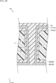
- the interconnecting through wiring portion 27 is formed so as to fill the space surrounded by the interconnecting insulating seed layer 39, and has a so-called solid configuration.
- the interconnecting through wiring portion 27 is tubular and laminated on the interconnecting insulating seed layer 39.
- a sixth insulating seed layer 36 is formed. The sixth insulating seed layer 36 is formed, for example, in the same process as forming the second insulating seed layer 32.
- This embodiment also makes it easier to manufacture electronic component A2. Furthermore, this embodiment makes it possible to protect the first functional element 1 with the sealing resin 5. Furthermore, by providing multiple interconnecting through-wiring portions 27, electronic component A2 can be mounted on a circuit board (not shown) or the like using terminal portions 282 located on the opposite side of electrode 11 in the z direction.
- First modified example of the second embodiment 29 shows a first modified example of the electronic component A2.
- the electronic component A21 of this modified example differs from the above-described embodiment mainly in that it includes a first functional element 1A and a second functional element 1B.
- the first functional element 1A and the second functional element 1B are elements that each perform a desired electrical function.
- the first functional element 1A and the second functional element 1B may have the same configuration or different configurations.
- the first functional element 1A and the second functional element 1B are arranged side by side in a direction perpendicular to the z direction (the x direction in the illustrated example) and are spaced apart from each other.
- the first functional element 1A and the second functional element 1B are surrounded by sealing resin 5.
- the first functional element 1A is exposed from the sealing resin 5 on both sides in the z direction.
- the second functional element 1B is covered by the sealing resin 5 on the other side in the z direction.
- the configuration of the first functional element 1A, the second functional element 1B, and the sealing resin 5 is not limited to the illustrated example.
- the first wiring layer 21 has a plurality of first wiring sections 211.
- the plurality of first wiring sections 211 are individually connected to the plurality of electrodes 11 of the first functional element 1A and the plurality of electrodes 11 of the second functional element 1B by a plurality of first through wiring sections 24.
- the second wiring layer 22 of this embodiment includes a second wiring portion 221 that provides electrical continuity between the electrode 11 of the first functional element 1A and the terminal portion 282.
- This second wiring portion 221 is connected to one first wiring portion 211 and one interconnecting through wiring portion 27.
- this second wiring portion 221 overlaps with the second functional element 1B, and reaches the through hole 51 from one first wiring portion 211, passing through the second functional element 1B in the x direction.
- This modified example also makes it easier to manufacture the electronic component A21. It also makes it easier to manufacture the electronic component A21 that incorporates multiple first functional elements 1A and second functional elements 1B together.
- Third embodiment 30 illustrates an electronic component according to a third embodiment of the present disclosure.
- An electronic component A3 according to this embodiment differs from the above-described embodiments mainly in that the electronic component A3 includes a first insulating layer 41, a second insulating layer 42, a third insulating layer 43, and a fourth insulating layer 44.
- the first insulating layer 41, the second insulating layer 42, the third insulating layer 43 and the fourth insulating layer 44 are each made of an insulating material containing, for example, epoxy resin.
- the first insulating layer 41 is interposed between the first functional element 1 and the first insulating seed layer 31.
- the first insulating layer 41 has a plurality of through holes 415. Each through hole 415 penetrates the first insulating layer 41 in the z direction and overlaps with one of the plurality of through holes 315 when viewed from the z direction.
- the first insulating layer 41 is also formed on the sealing resin 5.
- the first insulating layer 41 also has a plurality of through holes 416. The plurality of through holes 416 penetrate the first insulating layer 41 in the z direction and individually coincide with the plurality of through holes 51.
- the second insulating layer 42 is interposed between the first wiring portion 211 and the second insulating seed layer 32.
- the second insulating layer 42 is laminated on the first wiring layer 21 and the first insulating layer 41.
- the second insulating layer 42 has a plurality of through holes 425. Each through hole 425 overlaps with one of the plurality of through holes 325 when viewed from the z direction.
- the second insulating layer 42 also has a plurality of through holes 426. The plurality of through holes 426 penetrate the second insulating layer 42 in the z direction and individually coincide with the plurality of through holes 416.
- the third insulating layer 43 is interposed between the second wiring portion 221 and the third insulating seed layer 33.
- the third insulating layer 43 is laminated on the second wiring layer 22 and the second insulating layer 42.
- the third insulating layer 43 has a plurality of through holes 435. Each through hole 435 overlaps with one of the plurality of through holes 335 when viewed from the z direction.
- the third insulating layer 43 also has a plurality of through holes 436. The plurality of through holes 436 penetrate the third insulating layer 43 in the z direction and individually coincide with the plurality of through holes 426.
- the fourth insulating layer 44 is laminated on the third wiring layer 23 and the third insulating layer 43.
- the first insulating seed layer 31 of this embodiment includes a first activated region 310 and does not include the first inactivated region 311 described above.
- the first insulating seed layer 31 covers the inner surface of the through hole 415.
- the second insulating seed layer 32 of this embodiment includes a second activated region 320 and does not include the second inactivated region 321 described above.
- the second insulating seed layer 32 covers the inner surface of the through hole 425.
- the third insulating seed layer 33 of this embodiment includes a third activated region 330 and does not include the third inactivated region 331 described above.
- the third insulating seed layer 33 covers the inner surface of the through hole 435.
- the multiple first through wiring parts 24 are individually accommodated in the multiple through holes 315.
- the first through wiring parts 24 are in direct contact with the first activation region 310.
- No seed layer made of a metal such as Ti (titanium) is provided between the first through wiring parts 24 and the first activation region 310.
- the second through wiring parts 25 are individually housed in the through holes 325.
- the second through wiring parts 25 are in direct contact with the second activation region 320.
- No seed layer made of a metal such as Ti (titanium) is provided between the second through wiring parts 25 and the second activation region 320.
- the multiple third through wiring parts 26 are individually housed in the multiple through holes 335.
- the third through wiring parts 26 are in direct contact with the third activation region 330.
- No seed layer made of a metal such as Ti (titanium) is provided between the third through wiring parts 26 and the third activation region 330.
- the first functional element 1 is prepared and the sealing resin 5 is formed.
- the sealing resin 5 and the first insulating layer 41 are formed together using, for example, a compression molding technique.
- a plurality of through holes 415 are formed by irradiating the first insulating layer 41 with laser light L0.
- a first insulating seed layer 31 is formed.
- the multiple through holes 415 are filled with the first insulating seed layer 31.
- the first insulating seed layer 31 is irradiated with laser light L2. Desired portions of the first insulating seed layer 31 are removed with the laser light L2, and the remaining portions become a plurality of first activation regions 310. In addition, the laser light L2 is irradiated to portions of the first insulating seed layer 31 that will fill the through holes 415. As a result, a plurality of through holes 315 are formed.
- the first wiring layer 21 and the first through wiring parts 24 shown in FIG. 35 are formed by electroless plating or electroless plating and electroplating using the first activation regions 310 as a seed layer.
- the first wiring layer 21 includes the first wiring parts 211.
- the first through wiring parts 24 are formed in the through holes 315 and are in contact with the electrodes 11.
- the second insulating layer 42 is formed as shown in FIG. 36.
- the second insulating layer 42 is formed, for example, by a compression molding technique.
- the second insulating layer 42 is irradiated with laser light L0 to form a plurality of through holes 425.
- the plurality of through holes 425 overlap with the plurality of first wiring portions 211 when viewed in the z direction.
- a second insulating seed layer 32 is formed.
- the multiple through holes 425 are filled with the second insulating seed layer 32.
- the second insulating seed layer 32 is irradiated with laser light L2.
- the desired portions of the second insulating seed layer 32 are removed with the laser light L2, and the remaining portions become a plurality of second activation regions 320.
- the laser light L2 is irradiated to the portions of the second insulating seed layer 32 that will fill the through holes 425. As a result, a plurality of through holes 325 are formed.
- the second wiring layer 22 and the multiple second through wiring parts 25 shown in FIG. 40 are formed by electroless plating or electroless plating and electroplating using the multiple second activation regions 320 as a seed layer.
- the second wiring layer 22 includes multiple second wiring parts 221.
- the second through wiring parts 25 are formed in the through holes 325 and are in contact with the first wiring parts 211.
- the third insulating layer 43 is formed as shown in FIG. 31.
- the third insulating layer 43 is formed, for example, by a compression molding technique.
- a plurality of through holes 435 are formed by irradiating the third insulating layer 43 with laser light L0.
- the plurality of through holes 435 overlap with the plurality of second wiring portions 221 when viewed in the z direction.
- Laser light L0 is also irradiated to positions of the third insulating layer 43 that do not overlap with the first functional element 1 when viewed from the z direction.
- This irradiation of laser light L0 forms a through hole 436 in the third insulating layer 43, a through hole 426 in the second insulating layer 42, a through hole 416 in the first insulating layer 41, and a through hole 51 in the sealing resin 5.
- a third insulating seed layer 33, a back surface insulating seed layer 38 and a contact insulating seed layer 39 are formed.
- the third insulating seed layer 33 is irradiated with laser light L2 to form a plurality of third activation regions 330.
- the rear surface insulating seed layer 38 is irradiated with laser light L2 to form a plurality of rear surface activation regions 380.
- the first insulating seed layer 31, the second insulating seed layer 32, the third insulating seed layer 33 and the rear surface insulating seed layer 38 may be layers obtained by applying a polypyrrole dispersion liquid used in a polypyrrole plating method, for example.
- electroless plating or electroless plating and electroplating are performed using the multiple third activation regions 330, multiple backside activation regions 380, and multiple interconnect insulating seed layers 39 as seed layers to form the third wiring layer 23, backside wiring layer 28, and multiple interconnect through wiring parts 27 shown in FIG. 45.
- 44 shown in FIG. 30 is formed by, for example, a compression molding technique.
- This embodiment also makes it easier to manufacture electronic component A3. Furthermore, by providing first insulating layer 41, second insulating layer 42, third insulating layer 43, and fourth insulating layer 44, the insulation state of the parts of electronic component A3 that should be insulated can be maintained better.
- the first insulating layer 41, the second insulating layer 42, and the third insulating layer 43 it is possible to remove a portion of each of the first insulating seed layer 31, the second insulating seed layer 32, and the third insulating seed layer 33 with the laser light L, while avoiding the formation of unintended penetrations.
- the electronic components and methods for manufacturing electronic components according to the present disclosure are not limited to the above-described embodiments.
- the specific configurations of the electronic components and methods for manufacturing electronic components according to the present disclosure can be freely designed in various ways.
- the present disclosure includes the embodiments described in the following appendix.
- Appendix 1 A first functional element; a first insulating seed layer laminated on one side in a thickness direction of the first functional element; a first wiring layer laminated on the one side in the thickness direction of the first insulating seed layer.
- Appendix 2. The electronic component of claim 1, wherein the first insulating seed layer includes a first activated region in contact with the first wiring layer, and a first inactivated region away from the first wiring layer and in which the function as a seed layer to enable electroless plating has been inactivated.
- Appendix 3. 2.
- Appendix 4. the first insulating seed layer covers a portion of the first insulating layer; 4.
- Appendix 5. The electronic component according to claim 1, further comprising a first through wiring portion that penetrates the first insulating seed layer and is electrically connected to the first functional element and the first wiring layer.
- Appendix 6. The electronic component according to claim 5, wherein the first through wiring portion is integrally formed with the first wiring layer.
- the electronic component according to claim 5, wherein the first through wiring portion is formed of a conductive member separate from the first wiring layer.
- Appendix 8. a second insulating seed layer laminated on the one side of the first wiring layer in the thickness direction; 8.
- Appendix 9. The electronic component of claim 8, further comprising a second insulating layer interposed between the first wiring layer and the first insulating seed layer.
- Appendix 10. The electronic component according to claim 8 or 9, further comprising a second through wiring portion that penetrates the second insulating seed layer and is electrically connected to the first wiring layer and the second wiring layer.
- Appendix 12. 12 The electronic component according to claim 11, further comprising an interconnection through wiring portion that penetrates the sealing resin in the thickness direction.
- Appendix 13 The electronic component of claim 12, further comprising an interconnect insulating seed layer interposed between the sealing resin and the interconnect through wiring portion. Appendix 14. 14. The electronic component according to claim 11, further comprising a second functional element surrounded by the sealing resin as viewed in the thickness direction. Appendix 15. providing a first functional element; laminating a first insulating seed layer on one side of the first functional element in a thickness direction; forming a first wiring layer on the first insulating seed layer by electroless plating or by electroless plating and electroplating; A method for manufacturing an electronic component comprising the steps of: Appendix 16.
- Appendix 17. The method further includes a step of laminating a first insulating layer on the one side in the thickness direction of the first functional element before the step of laminating the first insulating seed layer, 17.
- the method for manufacturing an electronic component described in Appendix 16 wherein in the step of stacking the first insulating seed layer, the first insulating layer is interposed between the first functional element and the first insulating seed layer.
- Appendix 18 The method for manufacturing an electronic component described in Appendix 17, further comprising, after the step of stacking the first insulating seed layer and before the step of forming the first wiring layer, a step of removing a portion of the first insulating seed layer by irradiating with laser light.
- A1, A11, A12, A2, A21, A3 Electronic component 1, 1A: First functional element 1B: Second functional element 5: Sealing resin 11: Electrode 21: First wiring layer 22: Second wiring layer 23: Third wiring layer 24: First through wiring portion 25: Second through wiring portion 26: Third through wiring portion 27: Interconnecting through wiring portion 28: Back wiring layer 31: First insulating seed layer 32: Second insulating seed layer 33: Third insulating seed layer 36: Sixth insulating seed layer 38: Back insulating seed layer 39: Interconnecting insulating seed layer 41: First insulating layer 42: Second insulating layer 43: Third insulating layer 44: Fourth insulating layer 51: Through hole 211: First wiring portion 221: Second wiring portion 222: Terminal portion 232: Terminal portion 282: Terminal portion 310: First activated region 311: First inactivated region 315: Through hole 320: Second activated region 321: Second inactivated region 325: Through hole 330: Third activated region 331: Third inactivated region 335: Through
Landscapes
- Engineering & Computer Science (AREA)
- Manufacturing & Machinery (AREA)
- Microelectronics & Electronic Packaging (AREA)
- Production Of Multi-Layered Print Wiring Board (AREA)
Priority Applications (1)
| Application Number | Priority Date | Filing Date | Title |
|---|---|---|---|
| JP2025508267A JPWO2024195468A1 (https=) | 2023-03-20 | 2024-02-29 |
Applications Claiming Priority (2)
| Application Number | Priority Date | Filing Date | Title |
|---|---|---|---|
| JP2023-044198 | 2023-03-20 | ||
| JP2023044198 | 2023-03-20 |
Publications (1)
| Publication Number | Publication Date |
|---|---|
| WO2024195468A1 true WO2024195468A1 (ja) | 2024-09-26 |
Family
ID=92841906
Family Applications (1)
| Application Number | Title | Priority Date | Filing Date |
|---|---|---|---|
| PCT/JP2024/007527 Ceased WO2024195468A1 (ja) | 2023-03-20 | 2024-02-29 | 電子部品および電子部品の製造方法 |
Country Status (2)
| Country | Link |
|---|---|
| JP (1) | JPWO2024195468A1 (https=) |
| WO (1) | WO2024195468A1 (https=) |
Citations (7)
| Publication number | Priority date | Publication date | Assignee | Title |
|---|---|---|---|---|
| JPS616892A (ja) * | 1984-06-20 | 1986-01-13 | キヤノン株式会社 | プリント回路の製造方法 |
| JP2007525835A (ja) * | 2004-02-10 | 2007-09-06 | プラスティック ロジック リミテッド | 金属被着 |
| JP2012039090A (ja) * | 2010-07-15 | 2012-02-23 | Shinko Electric Ind Co Ltd | 半導体装置及びその製造方法 |
| JP2017028079A (ja) * | 2015-07-22 | 2017-02-02 | イビデン株式会社 | プリント配線板の製造方法およびプリント配線板 |
| JP2018037637A (ja) * | 2016-08-31 | 2018-03-08 | 株式会社東芝 | 半導体装置、及び半導体装置の製造方法 |
| WO2021193679A1 (ja) * | 2020-03-25 | 2021-09-30 | 株式会社イオックス | パターン形状の無電解めっき層を有するめっき物 |
| WO2023026363A1 (ja) * | 2021-08-24 | 2023-03-02 | 昭和電工マテリアルズ株式会社 | 電子部品装置を製造する方法、及び電子部品装置 |
-
2024
- 2024-02-29 JP JP2025508267A patent/JPWO2024195468A1/ja active Pending
- 2024-02-29 WO PCT/JP2024/007527 patent/WO2024195468A1/ja not_active Ceased
Patent Citations (7)
| Publication number | Priority date | Publication date | Assignee | Title |
|---|---|---|---|---|
| JPS616892A (ja) * | 1984-06-20 | 1986-01-13 | キヤノン株式会社 | プリント回路の製造方法 |
| JP2007525835A (ja) * | 2004-02-10 | 2007-09-06 | プラスティック ロジック リミテッド | 金属被着 |
| JP2012039090A (ja) * | 2010-07-15 | 2012-02-23 | Shinko Electric Ind Co Ltd | 半導体装置及びその製造方法 |
| JP2017028079A (ja) * | 2015-07-22 | 2017-02-02 | イビデン株式会社 | プリント配線板の製造方法およびプリント配線板 |
| JP2018037637A (ja) * | 2016-08-31 | 2018-03-08 | 株式会社東芝 | 半導体装置、及び半導体装置の製造方法 |
| WO2021193679A1 (ja) * | 2020-03-25 | 2021-09-30 | 株式会社イオックス | パターン形状の無電解めっき層を有するめっき物 |
| WO2023026363A1 (ja) * | 2021-08-24 | 2023-03-02 | 昭和電工マテリアルズ株式会社 | 電子部品装置を製造する方法、及び電子部品装置 |
Also Published As
| Publication number | Publication date |
|---|---|
| JPWO2024195468A1 (https=) | 2024-09-26 |
Similar Documents
| Publication | Publication Date | Title |
|---|---|---|
| US6489687B1 (en) | Semiconductor device and method of manufacturing the same, manufacturing device, circuit board, and electronic equipment | |
| US7102219B2 (en) | Semiconductor device, method of fabricating the same, stack-type semiconductor device, circuit board and electronic instrument | |
| US6744122B1 (en) | Semiconductor device, method of manufacture thereof, circuit board, and electronic device | |
| KR102151047B1 (ko) | 전력 오버레이 구조 및 그 제조 방법 | |
| US6395582B1 (en) | Methods for forming ground vias in semiconductor packages | |
| US20070080447A1 (en) | Electronic apparatus | |
| WO2005043622A1 (ja) | 半導体装置及びその製造方法 | |
| US20040135243A1 (en) | Semiconductor device, its manufacturing method and electronic device | |
| JP2011501410A (ja) | 頑健な多層配線要素および埋設された超小型電子素子とのアセンブリ | |
| CN1239588A (zh) | 带有通孔从焊球键合位置侧向偏移的tab带球栅阵列封装 | |
| US9338886B2 (en) | Substrate for mounting semiconductor, semiconductor device and method for manufacturing semiconductor device | |
| JP2002513510A (ja) | 電子デバイス用インターフェース構造 | |
| JP2001319992A (ja) | 配線基板、半導体装置及びそれらの製造方法 | |
| KR20020046966A (ko) | 반도체장치 및 그 제조방법 | |
| JP7154913B2 (ja) | 半導体装置及びその製造方法 | |
| US11862600B2 (en) | Method of forming a chip package and chip package | |
| JP4930204B2 (ja) | 半導体装置及びその製造方法 | |
| US20090045444A1 (en) | Integrated device and circuit system | |
| WO2024195468A1 (ja) | 電子部品および電子部品の製造方法 | |
| KR20230019926A (ko) | 반도체 장치 및 반도체 장치의 제조 방법 | |
| TW200933831A (en) | Integrated circuit package and the method for fabricating thereof | |
| US7696080B2 (en) | Method for manufacturing SIP semiconductor device | |
| JP6990029B2 (ja) | 電子機器および電子機器の製造方法 | |
| TW200901419A (en) | Packaging substrate surface structure and method for fabricating the same | |
| JP2024134092A (ja) | 回路部品、電子装置および回路部品の製造方法 |
Legal Events
| Date | Code | Title | Description |
|---|---|---|---|
| 121 | Ep: the epo has been informed by wipo that ep was designated in this application |
Ref document number: 24774613 Country of ref document: EP Kind code of ref document: A1 |
|
| ENP | Entry into the national phase |
Ref document number: 2025508267 Country of ref document: JP Kind code of ref document: A |
|
| WWE | Wipo information: entry into national phase |
Ref document number: 2025508267 Country of ref document: JP |
|
| NENP | Non-entry into the national phase |
Ref country code: DE |
|
| 122 | Ep: pct application non-entry in european phase |
Ref document number: 24774613 Country of ref document: EP Kind code of ref document: A1 |