WO2024190116A1 - 半導体装置及びその製造方法 - Google Patents
半導体装置及びその製造方法 Download PDFInfo
- Publication number
- WO2024190116A1 WO2024190116A1 PCT/JP2024/002595 JP2024002595W WO2024190116A1 WO 2024190116 A1 WO2024190116 A1 WO 2024190116A1 JP 2024002595 W JP2024002595 W JP 2024002595W WO 2024190116 A1 WO2024190116 A1 WO 2024190116A1
- Authority
- WO
- WIPO (PCT)
- Prior art keywords
- insulating layer
- oxide
- region
- layer
- oxide semiconductor
- Prior art date
- Legal status (The legal status is an assumption and is not a legal conclusion. Google has not performed a legal analysis and makes no representation as to the accuracy of the status listed.)
- Ceased
Links
Images










Classifications
-
- H—ELECTRICITY
- H10—SEMICONDUCTOR DEVICES; ELECTRIC SOLID-STATE DEVICES NOT OTHERWISE PROVIDED FOR
- H10D—INORGANIC ELECTRIC SEMICONDUCTOR DEVICES
- H10D30/00—Field-effect transistors [FET]
- H10D30/60—Insulated-gate field-effect transistors [IGFET]
- H10D30/67—Thin-film transistors [TFT]
- H10D30/674—Thin-film transistors [TFT] characterised by the active materials
- H10D30/6755—Oxide semiconductors, e.g. zinc oxide, copper aluminium oxide or cadmium stannate
-
- H—ELECTRICITY
- H10—SEMICONDUCTOR DEVICES; ELECTRIC SOLID-STATE DEVICES NOT OTHERWISE PROVIDED FOR
- H10D—INORGANIC ELECTRIC SEMICONDUCTOR DEVICES
- H10D30/00—Field-effect transistors [FET]
- H10D30/01—Manufacture or treatment
- H10D30/021—Manufacture or treatment of FETs having insulated gates [IGFET]
- H10D30/031—Manufacture or treatment of FETs having insulated gates [IGFET] of thin-film transistors [TFT]
- H10D30/0312—Manufacture or treatment of FETs having insulated gates [IGFET] of thin-film transistors [TFT] characterised by the gate electrodes
- H10D30/0314—Manufacture or treatment of FETs having insulated gates [IGFET] of thin-film transistors [TFT] characterised by the gate electrodes of lateral top-gate TFTs comprising only a single gate
-
- H—ELECTRICITY
- H10—SEMICONDUCTOR DEVICES; ELECTRIC SOLID-STATE DEVICES NOT OTHERWISE PROVIDED FOR
- H10D—INORGANIC ELECTRIC SEMICONDUCTOR DEVICES
- H10D30/00—Field-effect transistors [FET]
- H10D30/60—Insulated-gate field-effect transistors [IGFET]
- H10D30/67—Thin-film transistors [TFT]
- H10D30/6704—Thin-film transistors [TFT] having supplementary regions or layers in the thin films or in the insulated bulk substrates for controlling properties of the device
- H10D30/6723—Thin-film transistors [TFT] having supplementary regions or layers in the thin films or in the insulated bulk substrates for controlling properties of the device having light shields
-
- H—ELECTRICITY
- H10—SEMICONDUCTOR DEVICES; ELECTRIC SOLID-STATE DEVICES NOT OTHERWISE PROVIDED FOR
- H10D—INORGANIC ELECTRIC SEMICONDUCTOR DEVICES
- H10D30/00—Field-effect transistors [FET]
- H10D30/60—Insulated-gate field-effect transistors [IGFET]
- H10D30/67—Thin-film transistors [TFT]
- H10D30/6729—Thin-film transistors [TFT] characterised by the electrodes
- H10D30/673—Thin-film transistors [TFT] characterised by the electrodes characterised by the shapes, relative sizes or dispositions of the gate electrodes
- H10D30/6731—Top-gate only TFTs
-
- H—ELECTRICITY
- H10—SEMICONDUCTOR DEVICES; ELECTRIC SOLID-STATE DEVICES NOT OTHERWISE PROVIDED FOR
- H10D—INORGANIC ELECTRIC SEMICONDUCTOR DEVICES
- H10D62/00—Semiconductor bodies, or regions thereof, of devices having potential barriers
- H10D62/60—Impurity distributions or concentrations
Definitions
- One embodiment of the present invention relates to a semiconductor device that uses an oxide semiconductor as a channel and a method for manufacturing the same.
- semiconductor devices that use oxide semiconductor films as channels instead of silicon semiconductor films made of amorphous silicon, low-temperature polysilicon, and single crystal silicon have been developed (see, for example, Patent Documents 1 to 6).
- Semiconductor devices that include such oxide semiconductor films can be manufactured using a simple structure and low-temperature process, similar to thin-film transistors that include amorphous silicon films.
- semiconductor devices that include oxide semiconductor films are known to have higher field-effect mobility than semiconductor devices that include amorphous silicon films.
- oxide semiconductors carriers are generated when hydrogen is bonded to oxygen defects.
- oxygen defects are formed in an oxide semiconductor layer in a semiconductor device, and hydrogen is supplied to the oxygen defects to form source and drain regions, which are low-resistance regions.
- hydrogen diffuses into the channel region of the oxide semiconductor layer, its function as a channel of the semiconductor device is reduced.
- the diffusion of hydrogen into the channel region changes the threshold voltage in the electrical characteristics of the semiconductor device, increasing the variation in threshold voltage and reducing the manufacturing yield of the semiconductor device. Therefore, by using an oxide layer containing excess oxygen capable of trapping hydrogen as an insulating layer in contact with the oxide semiconductor layer, the intrusion of hydrogen into the channel region is suppressed.
- an oxide layer containing excess oxygen functions as an electron trap, and therefore the reliability of a semiconductor device containing such an oxide layer is significantly reduced. Therefore, there is a need for a semiconductor device that can suppress the decrease in reliability, supply hydrogen to the source and drain regions of the oxide semiconductor layer, and suppress the intrusion of hydrogen into the channel region of the oxide semiconductor layer.
- one embodiment of the present invention aims to provide a semiconductor device that includes a hydrogen trapping region that prevents hydrogen from entering the channel region.
- a semiconductor device includes an oxide insulating layer, an oxide semiconductor layer on the oxide insulating layer, a gate insulating layer on the oxide semiconductor layer, and a gate electrode on the gate insulating layer.
- the gate electrode contains impurities and does not contain the gate electrode.
- the oxide insulating layer, the oxide semiconductor layer, and the gate insulating layer contain impurities and do not contain the gate electrode and the oxide semiconductor layer.
- the oxide insulating layer and the gate insulating layer contain impurities.
- the concentration profile of the impurities includes a first peak and a second peak.
- a semiconductor device includes an oxide insulating layer, an oxide semiconductor layer on the oxide insulating layer, a gate insulating layer on the oxide semiconductor layer, and a gate electrode on the gate insulating layer.
- the gate electrode contains impurities and does not contain the gate electrode.
- the oxide semiconductor layer and the gate insulating layer contain impurities and do not contain the gate electrode and the oxide semiconductor layer.
- the oxide insulating layer and the gate insulating layer contain impurities, and the impurity concentration profile in the stacking direction in the third region includes a first peak and a second peak.
- a method for manufacturing a semiconductor device includes forming an oxide insulating layer, forming a mask layer having a first pattern on the oxide insulating layer, injecting a first impurity into the oxide insulating layer using the mask layer as a mask, forming an oxide semiconductor layer having a second pattern on the oxide insulating layer, covering the oxide semiconductor layer, forming a gate insulating layer on the oxide insulating layer and the oxide semiconductor layer, forming a gate electrode having a third pattern on the gate insulating layer, and injecting a second impurity into the oxide semiconductor layer using the gate electrode as a mask.
- a method for manufacturing a semiconductor device includes forming an oxide insulating layer, forming an oxide semiconductor layer having a first pattern on the oxide insulating layer, injecting a first impurity into the oxide insulating layer using a resist having the first pattern on which the oxide semiconductor layer is formed as a mask, covering the oxide semiconductor layer, forming a gate insulating layer on the oxide insulating layer and the oxide semiconductor layer, forming a gate electrode having a second pattern on the gate insulating layer, and injecting a second impurity into the oxide semiconductor layer using the gate electrode as a mask.
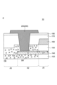
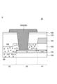
- 1 is a cross-sectional view showing an overview of a semiconductor device according to an embodiment of the present invention
- 1 is a plan view showing an overview of a semiconductor device according to an embodiment of the present invention
- 1 is a schematic enlarged partial cross-sectional view showing a configuration of a semiconductor device according to an embodiment of the present invention
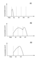
- 4 is a graph showing profiles of impurity concentrations in first to third regions in a semiconductor device according to one embodiment of the present invention.
- 4 is a graph showing profiles of impurity concentrations in first to third regions in a semiconductor device according to one embodiment of the present invention.
- 1 is a sequence diagram showing a method for manufacturing a semiconductor device according to an embodiment of the present invention
- 1A to 1C are cross-sectional views showing a method for manufacturing a semiconductor device according to an embodiment of the present invention.
- 1A to 1C are cross-sectional views showing a method for manufacturing a semiconductor device according to an embodiment of the present invention.
- 1A to 1C are cross-sectional views showing a method for manufacturing a semiconductor device according to an embodiment of the present invention.
- 1A to 1C are cross-sectional views showing a method for manufacturing a semiconductor device according to an embodiment of the present invention.
- 1A to 1C are cross-sectional views showing a method for manufacturing a semiconductor device according to an embodiment of the present invention.
- 1A to 1C are cross-sectional views showing a method for manufacturing a semiconductor device according to an embodiment of the present invention.
- 1A to 1C are cross-sectional views showing a method for manufacturing a semiconductor device according to an embodiment of the present invention.
- 1A to 1C are cross-sectional views showing a method for manufacturing a semiconductor device according to an embodiment of the present invention.
- 1A to 1C are cross-sectional views showing a method for manufacturing a semiconductor device according to an embodiment of the present invention.
- 1A to 1C are cross-sectional views showing a method for manufacturing a semiconductor device according to an embodiment of the present invention.
- 1A to 1C are cross-sectional views showing a method for manufacturing a semiconductor device according to an embodiment of the present invention.
- FIG. 1A to 1C are cross-sectional views showing a method for manufacturing a semiconductor device according to an embodiment of the present invention.
- 4 is a schematic cross-sectional view illustrating hydrogen trapping regions in a second region and a third region in a semiconductor device according to an embodiment of the present invention.
- FIG. 4 is a schematic cross-sectional view illustrating hydrogen trapping regions in a second region and a third region in a semiconductor device according to an embodiment of the present invention.
- FIG. 1 is a schematic enlarged partial cross-sectional view showing a configuration of a semiconductor device according to an embodiment of the present invention; 4 is a graph showing profiles of impurity concentrations in first to third regions in a semiconductor device according to one embodiment of the present invention.
- 1 is a sequence diagram showing a method for manufacturing a semiconductor device according to an embodiment of the present invention
- 1A to 1C are cross-sectional views showing a method for manufacturing a semiconductor device according to an embodiment of the present invention.
- 1A to 1C are cross-sectional views showing a method for manufacturing a semiconductor device according to an embodiment of the present invention.
- the direction from the substrate toward the oxide semiconductor layer is referred to as "up” or “upper”. Conversely, the direction from the oxide semiconductor layer toward the substrate is referred to as “down” or “downper”.
- up or downper are used in the explanation, but for example, the substrate and the oxide semiconductor layer may be arranged so that their hierarchical relationship is reversed from that shown in the figure.
- the expression "oxide semiconductor layer on a substrate” merely describes the hierarchical relationship between the substrate and the oxide semiconductor layer as described above, and other members may be arranged between the substrate and the oxide semiconductor layer.
- Up or “downper” refers to the order of stacking in a structure in which multiple layers are stacked, and when a pixel electrode is expressed above a transistor, the transistor and the pixel electrode may not overlap in a planar view. On the other hand, when a pixel electrode is expressed vertically above a transistor, it refers to a positional relationship in which the transistor and the pixel electrode overlap in a planar view.
- film and “layer” may be used interchangeably in some cases.
- the term “display device” refers to a structure that displays an image using an electro-optical layer.
- the term display device may refer to a display panel that includes an electro-optical layer, or may refer to a structure in which other optical components (e.g., polarizing components, backlights, touch panels, etc.) are attached to a display cell.
- the "electro-optical layer” may include a liquid crystal layer, an electroluminescent (EL) layer, an electrochromic (EC) layer, and an electrophoretic layer, unless technically inconsistent.
- a semiconductor device 10 according to an embodiment of the present invention will be described with reference to Figures 1 to 20.
- the semiconductor device 10 according to the embodiment described below may be used in an integrated circuit (IC) such as a microprocessor (Micro-Processing Unit: MPU) or a memory circuit, in addition to a transistor used in a display device.
- IC integrated circuit
- MPU Micro-Processing Unit
- MPU Memory-Processing Unit
- Figure 1 is a cross-sectional view showing an overview of the semiconductor device 10 according to one embodiment of the present invention.
- Figure 2 is a plan view showing an overview of the semiconductor device 10 according to one embodiment of the present invention.
- Figure 1 is a cross-sectional view taken along line AA' in Figure 2.
- the semiconductor device 10 is provided above a substrate 100.
- the semiconductor device 10 includes a light-shielding layer 105, a nitride insulating layer 110, an oxide insulating layer 120, an oxide semiconductor layer 140, a gate insulating layer 150, a gate electrode 160, insulating layers 170 and 180, a source electrode 201, and a drain electrode 203.
- the source electrode 201 and the drain electrode 203 are not particularly distinguished from each other, they may be collectively referred to as the source-drain electrodes 200.
- the light-shielding layer 105 is provided on the substrate 100.
- the nitride insulating layer 110 and the oxide insulating layer 120 are provided on the substrate 100 and the light-shielding layer 105.
- the nitride insulating layer 110 covers the upper surface and edges of the light-shielding layer 105.
- the oxide semiconductor layer 140 is provided on the oxide insulating layer 120.
- the oxide semiconductor layer 140 is patterned. A portion of the oxide insulating layer 120 extends beyond the edges of the oxide semiconductor layer 140 and outside the pattern of the oxide semiconductor layer 140.
- a configuration in which the oxide insulating layer 120 and the oxide semiconductor layer 140 are in contact with each other is illustrated, but the present invention is not limited to this configuration.
- a metal oxide layer may be provided between the oxide insulating layer 120 and the oxide semiconductor layer 140.
- a metal oxide containing aluminum as a main component may be used as the metal oxide layer.
- aluminum oxide may be used as the metal oxide layer.
- the gate insulating layer 150 covers the upper surface 141 and the side surface 143 of the oxide semiconductor layer 140 and is provided on the oxide semiconductor layer 140. That is, the upper surface 141 and the side surface 143 of the oxide semiconductor layer 140 are in contact with the gate insulating layer 150, and the lower surface 142 of the oxide semiconductor layer 140 is in contact with the oxide insulating layer 120.
- the gate electrode 160 is provided on the gate insulating layer 150 so as to face the oxide semiconductor layer 140.
- the insulating layer 170 is provided on the gate insulating layer 150 and the gate electrode 160.
- the insulating layer 170 covers the gate electrode 160.
- the insulating layer 180 is provided on the insulating layer 170.
- the insulating layers 170 and 180 are provided with openings 171 and 173 that reach the oxide semiconductor layer 140.
- the source electrode 201 is provided inside the opening 171.
- the source electrode 201 contacts the oxide semiconductor layer 140 at the bottom of the opening 171.
- the drain electrode 203 is provided inside the opening 173.
- the drain electrode 203 contacts the oxide semiconductor layer 140 at the bottom of the opening 173.
- the light-shielding layer 105 functions to block light incident on the oxide semiconductor layer 140 from the substrate 100 side.
- the nitride insulating layer 110 functions as a barrier film that blocks impurities diffusing from the substrate 100 toward the oxide semiconductor layer 140.
- the light-shielding layer 105 may also function as a bottom gate of the semiconductor device 10. In this case, the nitride insulating layer 110 and the oxide insulating layer 120 function as gate insulating layers for the bottom gate.
- the operation of the semiconductor device 10 is mainly controlled by the voltage supplied to the gate electrode 160.
- the light-shielding layer 105 functions as a bottom gate, an auxiliary voltage is supplied to the light-shielding layer 105.
- the same voltage as the gate electrode 160 may be supplied to the light-shielding layer 105.
- the light-shielding layer 105 is simply used as a light-shielding film, no specific voltage may be supplied to the light-shielding layer 105, and the potential of the light-shielding layer 105 may be floating.
- the light-shielding layer 105 may be an insulator.
- the semiconductor device 10 is divided into a first region A1, a second region A2, and a third region A3 based on the patterns of the gate electrode 160 and the oxide semiconductor layer 140.
- the first region A1 is a region that overlaps with the gate electrode 160 in a planar view.
- the oxide insulating layer 120, the oxide semiconductor layer 140, the gate insulating layer 150, and the gate electrode 160 are stacked in this order.
- the second region A2 is a region that does not overlap with the gate electrode 160 in a planar view, but overlaps with the oxide semiconductor layer 140.
- the oxide insulating layer 120, the oxide semiconductor layer 140, and the gate insulating layer 150 are stacked in this order.
- the third region A3 is a region that does not overlap with both the gate electrode 160 and the oxide semiconductor layer 140 in a planar view. In the third region A3, the oxide insulating layer 120 and the gate insulating layer 150 are stacked in this order.
- the thickness of the gate insulating layer 150 is, for example, 100 nm or more.
- the thickness of the gate insulating layer 150 may be 250 nm or more, or 300 nm or more.
- the oxide semiconductor layer 140 is divided into a source region S, a drain region D, and a channel region CH based on the pattern of the gate electrode 160.
- the source region S and the drain region D belong to the second region A2.
- the channel region CH belongs to the first region A1. In a plan view, the end of the channel region CH coincides with the end of the gate electrode 160.
- the oxide semiconductor layer 140 in the channel region CH has semiconductor properties.
- the oxide semiconductor layer 140 in each of the source region S and the drain region D has conductor properties. That is, the carrier concentration of the oxide semiconductor layer 140 in the source region S and the drain region D is higher than the carrier concentration of the oxide semiconductor layer 140 in the channel region CH.
- the source electrode 201 and the drain electrode 203 are in contact with the source region S and the drain region D, respectively, and are electrically connected to the oxide semiconductor layer 140.
- the oxide semiconductor layer 140 may have a single-layer structure or a multilayer structure.
- the semiconductor device 10 is exemplified by a top-gate transistor in which the gate electrode 160 is provided above the oxide semiconductor layer 140, but the present invention is not limited to this configuration.
- the semiconductor device 10 may be a dual-gate transistor in which the light-shielding layer 105 functions as a gate in addition to the gate electrode 160.
- the semiconductor device 10 may be a bottom-gate transistor in which the light-shielding layer 105 mainly functions as a gate.
- the above configuration is merely one embodiment, and the present invention is not limited to the above configuration.
- the width of the light-shielding layer 105 is greater than the width of the gate electrode 160.
- the D1 direction is the direction connecting the source electrode 201 and the drain electrode 203, and is the direction indicating the channel length L of the semiconductor device 10. Specifically, the length in the D1 direction in the region (channel region CH) where the oxide semiconductor layer 140 and the gate electrode 160 overlap is the channel length L, and the width in the D2 direction in the channel region CH is the channel width W.
- the light-shielding layer 105 and the gate electrode 160 extend in the D2 direction.
- FIG. 2 a configuration is illustrated in which the source/drain electrodes 200 do not overlap the light-shielding layer 105 and the gate electrode 160 in a plan view, but the present invention is not limited to this configuration.
- the source/drain electrodes 200 may overlap at least one of the light-shielding layer 105 and the gate electrode 160 in a plan view.
- the above configuration is merely one embodiment, and the present invention is not limited to the above configuration.
- a rigid substrate having light transmissivity such as a glass substrate, a quartz substrate, and a sapphire substrate
- a substrate containing a resin such as a polyimide substrate, an acrylic substrate, a siloxane substrate, or a fluororesin substrate
- impurities may be introduced into the resin in order to improve the heat resistance of the substrate 100.
- the substrate 100 does not need to be transparent, and therefore impurities that deteriorate the transparency of the substrate 100 may be used.
- a non-light transmissive substrate such as a semiconductor substrate such as a silicon substrate, a silicon carbide substrate, or a compound semiconductor substrate, or a conductive substrate such as a stainless steel substrate, is used as the substrate 100.
- General metal materials are used for the light-shielding layer 105, the gate electrode 160, and the source/drain electrodes 200.
- aluminum (Al), titanium (Ti), chromium (Cr), cobalt (Co), nickel (Ni), molybdenum (Mo), hafnium (Hf), tantalum (Ta), tungsten (W), bismuth (Bi), silver (Ag), copper (Cu), or alloys or compounds thereof are used for these members.
- the above materials may be used as a single layer or a laminated layer for the light-shielding layer 105, the gate electrode 160, and the source/drain electrodes 200.
- the light-shielding layer 105 may have a single-layer structure or a laminated structure.
- the light-shielding layer 105 may have a laminated structure of a red color filter, a green color filter, and a blue color filter.
- a general insulating material is used for the nitride insulating layer 110, the oxide insulating layer 120, and the insulating layers 170 and 180.
- an inorganic insulating layer such as silicon oxide (SiO x ), silicon oxynitride (SiO x N y ), aluminum oxide (AlO x ), or aluminum oxynitride (AlO x N y ) is used for the oxide insulating layer 120 and the insulating layer 180.
- An inorganic insulating layer such as silicon nitride (SiN x ), silicon nitride oxide (SiN x O y ), aluminum nitride (AlN x ), or aluminum nitride oxide (AlN x O y ) is used for the nitride insulating layer 110 and the insulating layer 170.
- an inorganic insulating layer such as silicon oxide (SiO x ), silicon oxynitride (SiO x N y ), aluminum oxide (AlO x ), or aluminum oxynitride (AlO x N y ) may be used for the insulating layer 170.
- an inorganic insulating layer such as silicon nitride (SiN x ), silicon oxynitride (SiN x O y ), aluminum nitride (AlN x ), or aluminum oxynitride (AlN x O y ) may be used.
- an insulating layer containing oxygen is used as the gate insulating layer 150.
- an inorganic insulating layer such as silicon oxide (SiO x ), silicon oxynitride (SiO x N y ), aluminum oxide (AlO x ), or aluminum oxynitride (AlO x N y ) is used as the gate insulating layer 150.
- an insulating layer having a function of releasing oxygen by heat treatment is used as the oxide insulating layer 120. That is, as the oxide insulating layer 120, an oxide insulating layer containing excess oxygen is used.
- the temperature of the heat treatment at which the oxide insulating layer 120 releases oxygen is, for example, 600°C or less, 500°C or less, 450°C or less, or 400°C or less. That is, the oxide insulating layer 120 releases oxygen at the heat treatment temperature performed in the manufacturing process of the semiconductor device 10 when a glass substrate is used as the substrate 100.
- At least one of the insulating layers 170 and 180 may be an insulating layer having a function of releasing oxygen by heat treatment, similar to the oxide insulating layer 120.
- an insulating layer with few defects is used as the gate insulating layer 150.
- the oxygen composition ratio in the gate insulating layer 150 is closer to the stoichiometric ratio for the insulating layer than the oxygen composition ratio in the other insulating layer.
- the oxygen composition ratio in the silicon oxide used as the gate insulating layer 150 is closer to the stoichiometric ratio of silicon oxide than the oxygen composition ratio in the silicon oxide used as the insulating layer 180.
- a layer in which no defects are observed when evaluated by electron spin resonance (ESR) may be used as the gate insulating layer 150.
- SiOxNy and AlOxNy are silicon compounds and aluminum compounds containing a smaller ratio ( x > y ) of nitrogen (N) than oxygen (O).
- SiNxOy and AlNxOy are silicon compounds and aluminum compounds containing a smaller ratio (x>y) of oxygen than nitrogen.
- a metal oxide having semiconductor properties can be used as the oxide semiconductor layer 140.
- an oxide semiconductor containing indium (In), gallium (Ga), zinc (Zn), and oxygen (O) can be used as the oxide semiconductor layer 140.
- the oxide semiconductor containing In, Ga, Zn, and O used in this embodiment is not limited to the above composition, and an oxide semiconductor having a different composition from the above may be used.
- an oxide semiconductor layer having a higher In ratio than the above may be used to improve mobility.
- an oxide semiconductor layer having a higher Ga ratio than the above may be used to increase the band gap and reduce the effect of light irradiation.
- an oxide semiconductor containing two or more metals including indium (In) may be used as the oxide semiconductor layer 140 having a ratio of In larger than the above.
- the ratio of indium to all metal elements in the oxide semiconductor layer 140 may be 50% or more in atomic ratio.
- gallium (Ga), zinc (Zn), aluminum (Al), hafnium (Hf), yttrium (Y), zirconia (Zr), and lanthanides may be used as the oxide semiconductor layer 140.
- Metal elements other than those listed above may also be used as the oxide semiconductor layer 140.
- oxide semiconductor layer 140 other elements may be added to an oxide semiconductor containing In, Ga, Zn, and O, for example, metal elements such as Al and Sn may be added.
- oxide semiconductors containing In and Ga IGO
- oxide semiconductors containing In and Zn IZO
- oxide semiconductors containing In, Sn, and Zn IGO
- oxide semiconductors containing In, Sn, and Zn IGO
- oxide semiconductors containing In, Sn, and Zn oxide semiconductors containing In and W
- oxide semiconductors containing In and W may also be used as the oxide semiconductor layer 140.
- the oxide semiconductor layer 140 When the ratio of indium is large, the oxide semiconductor layer 140 is likely to crystallize. As described above, by using a material in which the ratio of indium to all metal elements is 50% or more in the oxide semiconductor layer 140, it is possible to obtain an oxide semiconductor layer 140 having a polycrystalline structure. It is preferable to contain gallium as a metal element other than indium. Gallium belongs to the same Group 13 element as indium. Therefore, the crystallinity of the oxide semiconductor layer 140 is not inhibited by gallium, and the oxide semiconductor layer 140 has a polycrystalline structure.
- the oxide semiconductor layer 140 can be formed by a sputtering method.
- the composition of the oxide semiconductor layer 140 formed by the sputtering method depends on the composition of the sputtering target. Even if the oxide semiconductor layer 140 has a polycrystalline structure, the composition of the sputtering target and the composition of the oxide semiconductor layer 140 are approximately the same. In this case, the composition of the metal elements of the oxide semiconductor layer 140 can be determined based on the composition of the metal elements of the sputtering target.
- the composition of the oxide semiconductor layer may be identified using X-ray diffraction (XRD). Specifically, the composition of the metal elements in the oxide semiconductor layer can be identified based on the crystal structure and lattice constant of the oxide semiconductor layer obtained by XRD. Furthermore, the composition of the metal elements in the oxide semiconductor layer 140 can also be identified using X-ray fluorescence analysis or Electron Probe Micro Analyzer (EPMA) analysis. However, this is not the only possible method, since the oxygen contained in the oxide semiconductor layer 140 changes depending on the process conditions of sputtering, etc.
- XRD X-ray diffraction
- EPMA Electron Probe Micro Analyzer
- the oxide semiconductor layer 140 may have an amorphous structure or a polycrystalline structure.
- An oxide semiconductor having a polycrystalline structure can be manufactured using Poly-OS (Poly-crystalline Oxide Semiconductor) technology.
- Poly-OS Poly-crystalline Oxide Semiconductor
- an oxide semiconductor having a polycrystalline structure may be described as Poly-OS to distinguish it from an oxide semiconductor having an amorphous structure.
- the hydrogen trapping region is formed in the oxide insulating layer 120 and the gate insulating layer 150.
- the configuration of the hydrogen trapping region formed in the oxide insulating layer 120 and the gate insulating layer 150 will now be described with reference to FIGS.
- the source region S and drain region D of the oxide semiconductor layer 140 are formed by ion implantation of impurities using the gate electrode 160 as a mask, as described in detail below.
- impurities that can be used include boron (B), phosphorus (P), argon (Ar), and nitrogen (N).
- B boron
- P phosphorus
- Ar argon
- N nitrogen
- Si nitride contains more hydrogen than silicon oxide, so for example, by using silicon nitride as the insulating layer 170, hydrogen is diffused from the insulating layer 170, and the resistance of the source region S and drain region D can be reduced.
- the gate electrode 160 is used as a mask for the ion implantation of impurities, but the ion implantation of impurities is performed through the gate insulating layer 150 into the oxide semiconductor layer 140. Therefore, impurities are also introduced into the gate insulating layer 150 in the second region A2 and the third region A3, and a dangling bond defect DB is formed in the gate insulating layer 150. In addition, in the second region A2 and the third region A3, the impurities may pass through the oxide semiconductor layer 140 and the gate insulating layer 150 and be introduced into the oxide insulating layer 120.
- the ion implantation of impurities is performed into the oxide insulating layer 120 in addition to the ion implantation of the impurities described above.
- the dangling bond defects DB formed in the oxide insulating layer 120 and the gate insulating layer 150 trap hydrogen. That is, hydrogen trapping regions are formed in the oxide insulating layer 120 and the gate insulating layer 150 in the second region A2 and the third region A3. Therefore, for example, hydrogen diffused from the insulating layer 170 during the formation of the insulating layer 170 is trapped in the hydrogen trapping regions of the oxide insulating layer 120 and the gate insulating layer 150 in the second region A2 and the third region A3, so that the intrusion of hydrogen into the channel region CH can be suppressed.
- FIGS. 4 and 5 are graphs showing impurity concentration profiles in the first region A1 to the third region A3 in a semiconductor device according to one embodiment of the present invention.
- the vertical axis of each of the three concentration profiles shown in each of FIGS. 4 and 5 indicates the impurity concentration per unit volume (Concentration [/cm 3 ]), and the horizontal axis indicates the name of the layer in the stacking direction (film thickness direction).
- “UC” on the horizontal axis corresponds to the oxide insulating layer 120 and the nitride insulating layer 110.
- “OS” corresponds to the oxide semiconductor layer 140.
- GI corresponds to the gate insulating layer 150.
- GL corresponds to the gate electrode 160.
- PAS corresponds to the insulating layer 170.
- the impurity concentration profile has peaks in the oxide insulating layer 120 (UC) and the oxide semiconductor layer 140 (OS). That is, the second region A2 includes two peaks. In the stacking direction in the second region A2, the impurity concentration at the peak position of the oxide insulating layer 120 and the impurity concentration at the peak position of the oxide semiconductor layer 140 are greater than the impurity concentration contained in the gate insulating layer 150. Since the purpose of introducing the impurity in the second region A2 is to form the source region S and the drain region D, it is preferable, but not limited to, that the ion implantation conditions be set so as to obtain the above-mentioned concentration profile.
- the impurity concentration profile in the second region A2 may have peaks in the oxide insulating layer 120 (UC) and the gate insulating layer 150 (GI) (see FIG. 5).
- the impurity concentration at the peak position of the oxide insulating layer 120 and the impurity concentration at the peak position of the gate insulating layer 150 may be greater than the impurity concentration contained in the oxide semiconductor layer 140.
- the impurity concentration profile has a peak in the oxide insulating layer 120 (UC). That is, the third region A3 includes one peak. In the stacking direction in the third region A3, the impurity concentration at the peak position of the oxide insulating layer 120 may be greater than the impurity concentration contained in the gate insulating layer 150.
- the impurity concentration profile of the gate insulating layer 150 in the third region A3 is substantially the same as the impurity concentration profile of the gate insulating layer 150 in the second region A2. Therefore, the impurity concentration profile in the third region A3 shown in FIG. 5 may have peaks in the oxide insulating layer 120 (UC) and the gate insulating layer 150 (GI). In this case, the third region A3 includes two peaks.
- the impurity ion implantations are performed.
- the impurity is introduced into the oxide insulating layer 120 in the second region A2 and the third region A3.
- the impurity is introduced into the oxide insulating layer 120 in the second region A2 and the third region A3 via the gate insulating layer 150. Therefore, in the oxide insulating layer 120 in the first region A1, the second region A2, and the third region A3, the impurity concentration may increase in the order of the first region A1, the second region, and the third region.
- the concentration of the impurity contained at a predetermined position in the oxide insulating layer 120 in the stacking direction in the third region A3 is 1 ⁇ 10 16 /cm 3 or more, 1 ⁇ 10 17 /cm 3 or more, or 1 ⁇ 10 18 /cm 3 or more.
- the predetermined position may be a peak position of the concentration profile, or may be a position corresponding to the interface between the oxide insulating layer 120 and the gate insulating layer 150.
- the predetermined position may be a position shifted a predetermined depth in the direction of the oxide insulating layer 120 from a position corresponding to the interface.
- the channel region CH belongs to the first region A1, the source region S and the drain region D belong to the second region A2, and the regions other than the channel region CH, the source region S, and the drain region D belong to the third region A3. That is, the channel region CH is sandwiched between the second region A2 and surrounded by the third region A3. Therefore, for example, hydrogen diffused from the insulating layer 170 during the formation of the insulating layer 170 is trapped by the hydrogen trapping regions formed in the oxide insulating layer 120 and the gate insulating layer 150 in the second region A2 and the third region A3 located around the channel region CH. As a result, the hydrogen can be prevented from entering the channel region CH.
- FIG. 6 is a sequence diagram showing a method for manufacturing a semiconductor device according to an embodiment of the present invention.
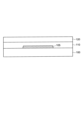
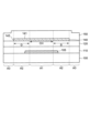
- Figs. 7 to 15 are cross-sectional views showing a method for manufacturing a semiconductor device according to an embodiment of the present invention.
- a light-shielding layer 105 is formed on a substrate 100, and a nitride insulating layer 110 and an oxide insulating layer 120 are formed on the light-shielding layer 105 (step S1010 "Insulating layer/light-shielding layer formation" in FIG. 6).
- silicon nitride is formed as the nitride insulating layer 110.
- silicon oxide is formed as the oxide insulating layer 120.
- the nitride insulating layer 110 and the oxide insulating layer 120 are formed by a chemical vapor deposition (CVD) method.
- the thickness of the nitride insulating layer 110 is 50 nm or more and 500 nm or less, or 150 nm or more and 300 nm or less.
- the thickness of the oxide insulating layer 120 is 50 nm or more and 500 nm or less, or 150 nm or more and 300 nm or less.
- the nitride insulating layer 110 can block impurities that diffuse from the substrate 100 toward the oxide semiconductor layer 140.
- the silicon oxide used as the oxide insulating layer 120 is silicon oxide that has the physical property of releasing oxygen by heat treatment.
- an oxide semiconductor layer 140 is formed on the oxide insulating layer 120 (step S1020 "OS film formation" in FIG. 6).
- the oxide semiconductor layer 140 is formed by sputtering or atomic layer deposition (ALD).
- the metal oxide layer is also formed by sputtering or atomic layer deposition in the same manner as described above.
- the thickness of the oxide semiconductor layer 140 is, for example, 10 nm to 100 nm, 15 nm to 70 nm, or 20 nm to 40 nm. In this embodiment, the thickness of the oxide semiconductor layer 140 is 30 nm. Before the heat treatment (OS annealing) described later, the oxide semiconductor layer 140 is amorphous.
- the oxide semiconductor layer 140 may contain microcrystals immediately after the film formation, which may hinder crystallization by subsequent OS annealing.
- the object to be formed can be formed while being cooled.
- the object to be formed can be cooled from the surface opposite to the surface to be formed so that the temperature of the surface to be formed of the object to be formed (hereinafter referred to as the "film formation temperature") is 100°C or less, 70°C or less, 50°C or less, or 30°C or less.
- the oxide semiconductor layer 140 having fewer crystalline components immediately after the film formation can be formed.
- the oxygen partial pressure in the film formation conditions for the oxide semiconductor layer 140 is 2% or more and 20% or less, 3% or more and 15% or less, or 3% or more and 10% or less.
- a pattern of the oxide semiconductor layer 140 is formed ("OS pattern formation" in step S1030 in FIG. 6).
- a resist mask is formed on the oxide semiconductor layer 140, and the oxide semiconductor layer 140 is etched using the resist mask.
- Wet etching or dry etching may be used for etching the oxide semiconductor layer 140.
- etching can be performed using an acidic etchant.
- oxalic acid, PAN, sulfuric acid, hydrogen peroxide solution, or hydrofluoric acid can be used as the etchant. Since the oxide semiconductor layer 140 in step S1020 is amorphous, the oxide semiconductor layer 140 can be easily patterned into a predetermined shape by wet etching.
- a heat treatment is performed on the oxide semiconductor layer 140 ("OS annealing" in step S1040 in FIG. 6).
- OS annealing the oxide semiconductor layer 140 is held at a predetermined temperature for a predetermined time.
- the predetermined temperature is 300° C. or higher and 500° C. or lower, or 350° C. or higher and 450° C. or lower.
- the holding time at the temperature is 15 minutes or higher and 120 minutes or lower, or 30 minutes or higher and 60 minutes or lower.
- the oxide semiconductor layer 140 is crystallized by this OS annealing. However, it is not necessary that the oxide semiconductor layer 140 is crystallized by the OS annealing.
- a mask layer 300 having a predetermined pattern is formed on the oxide semiconductor layer 140 (step S1050 "Formation of mask layer" in FIG. 6).
- the mask layer 300 may be formed using a resist or a metal.
- the mask layer 300 is patterned through a photolithography process.
- the predetermined pattern of the mask layer 300 may be substantially the same as the pattern of the gate electrode 160, or may be different.
- the mask layer 300 is formed so that the width of the mask layer 300 substantially matches the width of the gate electrode 160 in a cross-sectional view.
- impurity ions are implanted into the oxide insulating layer 120 using the mask layer 300 as a mask ("first ion implantation" in step S1060 in FIG. 6).
- first ion implantation for example, boron (B), phosphorus (P), argon (Ar), or nitrogen (N) is used as the impurity.
- impurities such as boron (B), phosphorus (P), argon (Ar), or nitrogen (N) are introduced into the oxide insulating layer 120.
- the impurities introduced into the oxide insulating layer 120 form dangling bond defects DB.
- the region of the oxide insulating layer 120 where the dangling bond defects DB are formed can function as a hydrogen trapping region.
- the first ion implantation in step S1060 it is important to form a dangling bond defect DB in the oxide insulating layer 120 while not forming a dangling bond defect DB in the nitride insulating layer 110. Therefore, in the first ion implantation, impurity ions are implanted so as to have a concentration profile with a peak in the oxide insulating layer 120.
- the position of the peak and the amount of impurity can be controlled by adjusting the process parameters of the ion implantation (e.g., dose, acceleration voltage, plasma power, etc.).
- the dose is 1 ⁇ 10 14 /cm 2 or more, 5 ⁇ 10 14 /cm 2 , or 1 ⁇ 10 15 /cm 2 or more.
- the acceleration voltage is more than 10 keV, 15 keV or more, or 20 keV or more.
- step S1060 impurities are also introduced into the oxide semiconductor layer 140. Therefore, oxygen defects are formed in the oxide semiconductor layer 140, and the source region S and the drain region D are formed. However, in step S1060, it is not necessary that sufficient oxygen defects are formed in the oxide semiconductor layer 140.
- the gate insulating layer 150 is formed (step S1070 "GI formation" in FIG. 6).
- silicon oxide is formed as the gate insulating layer 150.
- the gate insulating layer 150 is formed by a CVD method.
- the gate insulating layer 150 may be formed at a film formation temperature of 350° C. or higher.
- the thickness of the gate insulating layer 150 is, for example, 100 nm to 500 nm, 200 nm to 400 nm, or 250 nm to 350 nm.
- a process of implanting oxygen into the upper part of the gate insulating layer 150 may be performed.
- a configuration in which a metal oxide layer is formed on the gate insulating layer 150 by a sputtering method may be performed.
- a heat treatment is performed to supply oxygen to the oxide semiconductor layer 140 (step S1080 "oxidation anneal" in FIG. 6).
- oxidation anneal oxygen released from the oxide insulating layer 120 and the gate insulating layer 150 is supplied to the oxide semiconductor layer 140, and the oxygen vacancies are repaired.
- the oxidation anneal may be performed in a state where an insulating layer that releases oxygen by heat treatment is formed on the gate insulating layer 150.
- a metal oxide layer mainly composed of aluminum may be formed on the gate insulating layer 150 by a sputtering method, and oxidation annealing may be performed in this state.
- aluminum oxide which has high barrier properties against gas, as this metal oxide layer, it is possible to suppress outward diffusion of oxygen implanted into the gate insulating layer 150 during oxidation annealing.
- the oxygen implanted into the gate insulating layer 150 is efficiently supplied to the oxide semiconductor layer 140.
- the gate electrode 160 is formed and patterned (step S1090 "GE formation" in FIG. 6).
- the gate electrode 160 is formed by sputtering or atomic layer deposition.
- the gate electrode 160 is patterned through a photolithography process.
- impurity ions are implanted into the oxide semiconductor layer 140 using the gate electrode 160 as a mask ("second ion implantation" in step S1100 in FIG. 6).
- second ion implantation for example, boron (B), phosphorus (P), argon (Ar), or nitrogen (N) is used as the impurity.
- the impurity in the second ion implantation in step S1090 may be the same as or different from the impurity in the first ion implantation in step S1060.
- boron (B), phosphorus (P), argon (Ar), nitrogen (N), or the like is introduced into the oxide semiconductor layer 140.
- the gate electrode 160 is used as a mask. Therefore, impurities are introduced into the oxide semiconductor layer 140 in the region that does not overlap with the gate electrode 160, and oxygen defects are formed. Hydrogen is bonded to the generated oxygen defects, and the resistance of the oxide semiconductor layer 140 decreases. That is, a source region S and a drain region D are formed in the oxide semiconductor layer 140. On the other hand, impurities are not introduced into the region of the oxide semiconductor layer 140 that overlaps with the gate electrode 160, and no oxygen defects are formed. That is, a channel region CH is formed in the oxide semiconductor layer 140. Note that impurities are introduced into the gate electrode 160 used as a mask.
- impurities are also introduced into the gate insulating layer 150 and the oxide insulating layer 120.
- the impurities introduced into the gate insulating layer 150 and the oxide insulating layer 120 form dangling bond defects DB.
- the regions of the gate insulating layer 150 and the oxide insulating layer 120 where the dangling bond defects DB are formed can function as hydrogen trapping regions.
- the first ion implantation in step S1060 and the second ion implantation in step S1100 form a first region A1, a second region A2, and a third region A3.
- the gate electrode 160 contains impurities.
- the oxide insulating layer 120, the oxide semiconductor layer 140, and the gate insulating layer 150 contain impurities.
- the oxide semiconductor layer 140 in the second region A2 functions as a source region or a drain region.
- the oxide insulating layer 120 and the gate insulating layer 150 in the second region A2 function as a hydrogen trapping region.
- the oxide insulating layer 120 and the gate insulating layer 150 contain impurities.
- the oxide insulating layer 120 and the gate insulating layer 150 in the third region A3 function as a hydrogen trapping region.
- impurity ions are implanted so as to have a concentration profile having a peak in one of the oxide semiconductor layer 140 and the gate insulating layer 150 in the second region A2.
- the position of the peak and the amount of impurity can be controlled by adjusting the process parameters of the ion implantation (e.g., dose, acceleration voltage, plasma power, etc.).
- the dose is 1 ⁇ 10 14 /cm 2 or more, 5 ⁇ 10 14 /cm 2 , or 1 ⁇ 10 15 /cm 2 or more.
- the acceleration voltage is more than 10 keV, 15 keV or more, or 20 keV or more.
- Hydrogen is introduced into the oxygen defects in the source region S and drain region D to reduce their resistance.
- the channel region CH also becomes less resistant, causing humps or depression, and thus deteriorating the electrical characteristics of the semiconductor device. Therefore, it is necessary to form a hydrogen trapping region that suppresses hydrogen from penetrating into the channel region CH.
- a hydrogen trapping region is formed not only in the gate insulating layer 150 but also in the oxide insulating layer 120.
- a first ion implantation is performed in step S1060 to form a hydrogen trapping region in the oxide insulating layer 120.
- the thickness of the gate insulating layer 150 is large (for example, when the thickness of the gate insulating layer 150 is 200 nm or more), sufficient impurities can be ion-implanted into the oxide insulating layer 120 to form dangling bond defects DB, thereby forming a hydrogen trapping region.
- insulating layers 170, 180 are formed as interlayer films on the gate insulating layer 150 and the gate electrode 160 (step S1110 "Interlayer film formation" in Figure 6).
- the insulating layers 170, 180 are formed by a CVD method.
- a silicon nitride layer is formed as the insulating layer 170
- a silicon oxide layer is formed as the insulating layer 180.
- the materials used for the insulating layers 170, 180 are not limited to the above.
- the thickness of the insulating layer 170 is 50 nm or more and 500 nm or less.
- the thickness of the insulating layer 180 is 50 nm or more and 500 nm or less.
- openings 171, 173 are formed in insulating layers 170, 180 ("contact hole” in step S1120 in Figure 6).
- the source region S is exposed through opening 171.
- the drain region D is exposed through opening 173.
- source/drain electrodes 200 are formed on the source region S and drain region D exposed through openings 171, 173 and on insulating layer 180 ("SD formation" in step S1130 in Figure 6), the semiconductor device 10 shown in Figure 1 is completed.
- steps S1050 and S1060 may be performed after step S1010.
- a mask layer 300 having a predetermined pattern is formed on the oxide insulating layer 120 (see FIG. 17).
- impurity ions are implanted into the oxide insulating layer 120 using the mask layer 300 as a mask (see FIG. 18).
- steps S1020 to S1040 and steps S1070 to S1130 are performed in order.
- Hydrogen traps in dangling bond defects DB] 19 and 20 are schematic cross-sectional views illustrating hydrogen trapping regions in the second and third regions in a semiconductor device according to one embodiment of the present invention.
- impurities are introduced into the oxide insulating layer 120 and the gate insulating layer 150 in the second region A2 and the third region A3 by the first ion implantation in step S1060 and the second ion implantation in step S1100, and dangling bond defects DB are formed in the oxide insulating layer 120 and the gate insulating layer 150 in the second region A2 and the third region A3.
- the insulating layer 170 In order for the insulating layer 170 to have the function of blocking impurities diffused from above, it is preferable that the insulating layer 170 is a dense film with few defects. In order to obtain such an insulating layer 170, it is necessary to form the insulating layer 170 at a high temperature. For example, when a silicon nitride layer is formed as the insulating layer 170, the insulating layer 170 contains a large amount of hydrogen, and a large amount of hydrogen diffuses from the insulating layer 170 to the oxide insulating layer 120, the oxide semiconductor layer 140, and the gate insulating layer 150 due to the film formation temperature.
- step S1110 hydrogen H diffused from the insulating layer 170 during or after the formation can be prevented from penetrating into the channel region CH.
- the insulating layer 170 since a film containing a large amount of hydrogen can be used as the insulating layer 170, an insulating layer 170 having a high impurity blocking function can be realized. Furthermore, the resistance of the oxide semiconductor layer 140 in the source region S and the drain region D can be sufficiently reduced.
- the amount of trapped hydrogen H may increase in the order of the oxide insulating layer 120 in the first region A1, the oxide insulating layer 120 in the second region A2, and the oxide insulating layer 120 in the third region A3.
- the hydrogen trapping region is formed in the oxide insulating layer 120 and the gate insulating layer 150.
- the configuration of the hydrogen trapping region formed in the oxide insulating layer 120 and the gate insulating layer 150 will now be described with reference to FIGS.
- FIG. 21 is a schematic partially enlarged cross-sectional view showing the configuration of a semiconductor device according to one embodiment of the present invention. Specifically, FIG. 21 is an enlarged cross-sectional view of region P in FIG. 1. Region P shown in FIG. 21 is a region near the drain region D, but the region near the source region S also has a similar configuration to region P.
- the gate electrode 160 is used as a mask for the ion implantation of impurities to form the source region S and the drain region D, but the ion implantation of impurities is performed through the gate insulating layer 150 into the oxide semiconductor layer 140. Therefore, impurities are also introduced into the gate insulating layer 150 in the second region A2 and the third region A3, and dangling bond defects DB are formed in the gate insulating layer 150. In addition, in the second region A2 and the third region A3, the impurities may pass through the oxide semiconductor layer 140 and the gate insulating layer 150 and be introduced into the oxide insulating layer 120.
- impurity ions are implanted into the oxide insulating layer 120 separately from the ion implantation of the impurities described above.
- a dangling bond defect DB is formed in the gate insulating layer 150
- a dangling bond defect DB is formed in the oxide insulating layer 120 and the gate insulating layer 150.
- silicon oxide is used for each of the oxide insulating layer 120 and the gate insulating layer 150
- a silicon dangling bond defect DB is formed in the oxide insulating layer 120 and the gate insulating layer 150.
- FIGS. 22 and 23 are graphs showing impurity concentration profiles in the first region A1 to the third region A3 in a semiconductor device according to one embodiment of the present invention.
- the vertical axis of each of the three concentration profiles shown in each of FIGS. 22 and 23 indicates the impurity concentration per unit volume (Concentration [/cm 3 ]), and the horizontal axis indicates the name of the layer in the stacking direction (film thickness direction).
- “UC” on the horizontal axis corresponds to the oxide insulating layer 120 and the nitride insulating layer 110.
- “OS” corresponds to the oxide semiconductor layer 140.
- GI corresponds to the gate insulating layer 150.
- GL corresponds to the gate electrode 160.
- PAS corresponds to the insulating layer 170.
- the concentration profile of the impurity has a peak in the gate electrode 160 (GL). That is, the first region A1 includes one peak.
- Metallic materials have a high blocking ability for impurities introduced by ion implantation. When a metallic material is used as the gate electrode 160, the impurities are blocked by the gate electrode 160 and do not reach the gate insulating layer 150 (GI). Therefore, dangling bond defects DB due to the introduction of impurities are not formed in the gate insulating layer 150 in the first region A1. However, the impurities may reach the gate insulating layer 150 as long as they do not affect the electrical characteristics of the semiconductor device 10.
- the impurity concentration profile has a peak in the oxide semiconductor layer 140 (OS). That is, the second region A2 includes one peak. In the stacking direction in the second region A2, the impurity concentration at the peak position of the oxide semiconductor layer 140 is greater than the impurity concentration contained in the gate insulating layer 150. Since the purpose of introducing the impurity in the second region A2 is to form the source region S and the drain region D, it is preferable, but not limited to, that the ion implantation conditions be set so as to obtain the above-mentioned concentration profile.
- the impurity concentration profile in the second region A2 may have a peak in the gate insulating layer 150 (GI) (see FIG. 23). In this case, in the stacking direction in the second region A2, the impurity concentration at the peak position of the gate insulating layer 150 is greater than the impurity concentration contained in the oxide semiconductor layer 140.
- GI gate insulating layer 150
- the impurity concentration profile has a peak in the oxide insulating layer 120 (UC). That is, the third region A3 includes one peak. In the stacking direction in the third region A3, the impurity concentration at the peak position of the oxide insulating layer 120 is greater than the impurity concentration contained in the gate insulating layer 150.
- the impurity concentration profile of the gate insulating layer 150 in the third region A3 is substantially the same as the impurity concentration profile of the gate insulating layer 150 in the second region A2. Therefore, the impurity concentration profile in the third region A3 shown in FIG. 23 may have peaks in the oxide insulating layer 120 (UC) and the gate insulating layer 150 (GI). In this case, the third region A3 includes two peaks.
- the impurity ion implantations are performed.
- the impurity is introduced into the oxide insulating layer 120 in the third region A3.
- the impurity is introduced into the oxide insulating layer 120 in the second region A2 and the third region A3 through the gate insulating layer 150.
- the impurity may be introduced into the oxide insulating layer 120. Therefore, in the oxide insulating layer 120 in the first region A1, the second region A2, and the third region A3, the impurity concentration may increase in the order of the first region A1, the second region A2, and the third region A3.
- the impurity concentration of the oxide insulating layer 120 in the second region A2 is less than 1 ⁇ 10 16 /cm 3 .
- the concentration of the impurity contained at a predetermined position in the oxide insulating layer 120 in the stacking direction in the third region A3 is 1 ⁇ 10 16 /cm 3 or more, 1 ⁇ 10 17 /cm 3 or more, or 1 ⁇ 10 18 /cm 3 or more.
- the predetermined position may be a peak position of the concentration profile, or may be a position corresponding to the interface between the oxide insulating layer 120 and the gate insulating layer 150.
- the predetermined position may be a position shifted a predetermined depth in the direction of the oxide insulating layer 120 from a position corresponding to the interface.
- the channel region CH belongs to the first region A1, the source region S and the drain region D belong to the second region A2, and the regions other than the channel region CH, the source region S, and the drain region D belong to the third region A3. That is, the channel region CH is sandwiched between the second region A2 and surrounded by the third region A3. Therefore, for example, hydrogen diffused from the insulating layer 170 during the formation of the insulating layer 170 is trapped by the hydrogen trapping regions formed in the gate insulating layer 150 in the second region A2 and the third region A3 located around the channel region CH and in the oxide insulating layer 120 in the third region A3. As a result, the hydrogen can be prevented from entering the channel region CH.
- FIG. 24 is a sequence diagram showing a method for manufacturing a semiconductor device according to an embodiment of the present invention.
- Figs. 25 and 26 are cross-sectional views showing a method for manufacturing a semiconductor device according to an embodiment of the present invention.
- Steps S2010 to S2030 shown in FIG. 24 are similar to steps S1010 to S1030 shown in FIG. 5. However, in step S2030, as shown in FIG. 25, the resist mask 310 used in patterning the oxide semiconductor layer 140 is not removed but is left as it is.
- impurity ions are implanted into the oxide insulating layer 120 using the resist mask 310 as a mask ("first ion implantation" in step S2040 in FIG. 24).
- first ion implantation for example, boron (B), phosphorus (P), argon (Ar), or nitrogen (N) is used as the impurity.
- impurities such as boron (B), phosphorus (P), argon (Ar), or nitrogen (N) are introduced into the oxide insulating layer 120.
- the impurities introduced into the oxide insulating layer 120 form dangling bond defects DB.
- the region of the oxide insulating layer 120 where the dangling bond defects DB are formed can function as a hydrogen trapping region.
- the first ion implantation in step S2040 it is important to form a dangling bond defect DB in the oxide insulating layer 120 while not forming a dangling bond defect DB in the nitride insulating layer 110. Therefore, in the first ion implantation, impurity ions are implanted so as to have a concentration profile with a peak in the oxide insulating layer 120.
- the position of the peak and the amount of impurity can be controlled by adjusting the process parameters of the ion implantation (e.g., dose, acceleration voltage, plasma power, etc.).
- the dose is 1 ⁇ 10 14 /cm 2 or more, 5 ⁇ 10 14 /cm 2 , or 1 ⁇ 10 15 /cm 2 or more.
- the acceleration voltage is more than 10 keV, 15 keV or more, or 20 keV or more.
- the resist mask 310 is removed.
- step S2040 After the first ion implantation in step S2040, a heat treatment (OS anneal) is performed on the oxide semiconductor layer 140 ("OS anneal" in step S2050 in FIG. 24). Step S2040 is similar to step S1050.
- Steps S2060 to S2120 shown in FIG. 24 are similar to steps S1070 to S1130 shown in FIG. 5.
- the amount of trapped hydrogen H may increase in the order of the oxide insulating layer 120 in the first region A1, the oxide insulating layer 120 in the second region A2, and the oxide insulating layer 120 in the third region A3.
Landscapes
- Thin Film Transistor (AREA)
Priority Applications (3)
| Application Number | Priority Date | Filing Date | Title |
|---|---|---|---|
| CN202480014051.1A CN120753017A (zh) | 2023-03-16 | 2024-01-29 | 半导体装置及其制造方法 |
| JP2025506537A JPWO2024190116A1 (https=) | 2023-03-16 | 2024-01-29 | |
| US19/322,823 US20260006828A1 (en) | 2023-03-16 | 2025-09-09 | Semiconductor device and manufacturing method thereof |
Applications Claiming Priority (2)
| Application Number | Priority Date | Filing Date | Title |
|---|---|---|---|
| JP2023-041930 | 2023-03-16 | ||
| JP2023041930 | 2023-03-16 |
Related Child Applications (1)
| Application Number | Title | Priority Date | Filing Date |
|---|---|---|---|
| US19/322,823 Continuation US20260006828A1 (en) | 2023-03-16 | 2025-09-09 | Semiconductor device and manufacturing method thereof |
Publications (1)
| Publication Number | Publication Date |
|---|---|
| WO2024190116A1 true WO2024190116A1 (ja) | 2024-09-19 |
Family
ID=92754751
Family Applications (1)
| Application Number | Title | Priority Date | Filing Date |
|---|---|---|---|
| PCT/JP2024/002595 Ceased WO2024190116A1 (ja) | 2023-03-16 | 2024-01-29 | 半導体装置及びその製造方法 |
Country Status (4)
| Country | Link |
|---|---|
| US (1) | US20260006828A1 (https=) |
| JP (1) | JPWO2024190116A1 (https=) |
| CN (1) | CN120753017A (https=) |
| WO (1) | WO2024190116A1 (https=) |
Citations (10)
| Publication number | Priority date | Publication date | Assignee | Title |
|---|---|---|---|---|
| JP2003031587A (ja) * | 2001-07-17 | 2003-01-31 | Semiconductor Energy Lab Co Ltd | 半導体装置およびその作製方法 |
| JP2007294491A (ja) * | 2006-04-20 | 2007-11-08 | Mitsubishi Electric Corp | 薄膜トランジスタ、及びその製造方法、並びに、アクティブマトリクス型表示装置及びその製造方法 |
| WO2009011084A1 (ja) * | 2007-07-17 | 2009-01-22 | Sharp Kabushiki Kaisha | 薄膜トランジスタを備えた半導体装置およびその製造方法 |
| JP2009123732A (ja) * | 2007-11-12 | 2009-06-04 | Seiko Epson Corp | 半導体装置の製造方法、電気光学装置の製造方法 |
| JP2009135448A (ja) * | 2007-11-01 | 2009-06-18 | Semiconductor Energy Lab Co Ltd | 半導体基板の作製方法及び半導体装置の作製方法 |
| JP2011258939A (ja) * | 2010-05-14 | 2011-12-22 | Semiconductor Energy Lab Co Ltd | 半導体装置の作製方法 |
| JP2012238851A (ja) * | 2011-04-27 | 2012-12-06 | Semiconductor Energy Lab Co Ltd | 半導体装置の作製方法 |
| JP2015144258A (ja) * | 2013-12-26 | 2015-08-06 | 株式会社半導体エネルギー研究所 | 半導体装置 |
| JP2017107913A (ja) * | 2015-12-07 | 2017-06-15 | 株式会社ジャパンディスプレイ | 薄膜トランジスタ及び薄膜トランジスタの製造方法 |
| WO2019166906A1 (ja) * | 2018-02-28 | 2019-09-06 | 株式会社半導体エネルギー研究所 | 半導体装置、および半導体装置の作製方法 |
-
2024
- 2024-01-29 JP JP2025506537A patent/JPWO2024190116A1/ja active Pending
- 2024-01-29 CN CN202480014051.1A patent/CN120753017A/zh active Pending
- 2024-01-29 WO PCT/JP2024/002595 patent/WO2024190116A1/ja not_active Ceased
-
2025
- 2025-09-09 US US19/322,823 patent/US20260006828A1/en active Pending
Patent Citations (10)
| Publication number | Priority date | Publication date | Assignee | Title |
|---|---|---|---|---|
| JP2003031587A (ja) * | 2001-07-17 | 2003-01-31 | Semiconductor Energy Lab Co Ltd | 半導体装置およびその作製方法 |
| JP2007294491A (ja) * | 2006-04-20 | 2007-11-08 | Mitsubishi Electric Corp | 薄膜トランジスタ、及びその製造方法、並びに、アクティブマトリクス型表示装置及びその製造方法 |
| WO2009011084A1 (ja) * | 2007-07-17 | 2009-01-22 | Sharp Kabushiki Kaisha | 薄膜トランジスタを備えた半導体装置およびその製造方法 |
| JP2009135448A (ja) * | 2007-11-01 | 2009-06-18 | Semiconductor Energy Lab Co Ltd | 半導体基板の作製方法及び半導体装置の作製方法 |
| JP2009123732A (ja) * | 2007-11-12 | 2009-06-04 | Seiko Epson Corp | 半導体装置の製造方法、電気光学装置の製造方法 |
| JP2011258939A (ja) * | 2010-05-14 | 2011-12-22 | Semiconductor Energy Lab Co Ltd | 半導体装置の作製方法 |
| JP2012238851A (ja) * | 2011-04-27 | 2012-12-06 | Semiconductor Energy Lab Co Ltd | 半導体装置の作製方法 |
| JP2015144258A (ja) * | 2013-12-26 | 2015-08-06 | 株式会社半導体エネルギー研究所 | 半導体装置 |
| JP2017107913A (ja) * | 2015-12-07 | 2017-06-15 | 株式会社ジャパンディスプレイ | 薄膜トランジスタ及び薄膜トランジスタの製造方法 |
| WO2019166906A1 (ja) * | 2018-02-28 | 2019-09-06 | 株式会社半導体エネルギー研究所 | 半導体装置、および半導体装置の作製方法 |
Also Published As
| Publication number | Publication date |
|---|---|
| CN120753017A (zh) | 2025-10-03 |
| US20260006828A1 (en) | 2026-01-01 |
| JPWO2024190116A1 (https=) | 2024-09-19 |
Similar Documents
| Publication | Publication Date | Title |
|---|---|---|
| US20240113227A1 (en) | Semiconductor device | |
| JP2024051551A5 (https=) | ||
| WO2024190116A1 (ja) | 半導体装置及びその製造方法 | |
| WO2024190115A1 (ja) | 半導体装置及びその製造方法 | |
| JPWO2024190116A5 (https=) | ||
| JPWO2024190115A5 (https=) | ||
| US20240113228A1 (en) | Semiconductor device and method for manufacturing semiconductor device | |
| TWI902041B (zh) | 半導體裝置 | |
| JP2025128517A (ja) | 半導体装置 | |
| TWI857754B (zh) | 半導體裝置 | |
| JP2024053987A5 (https=) | ||
| US20250113543A1 (en) | Semiconductor device | |
| US20250113546A1 (en) | Semiconductor device | |
| JP2025140590A (ja) | 半導体装置 | |
| JP2025060044A (ja) | 半導体装置 | |
| JP2024039361A5 (https=) | ||
| JP2025059498A (ja) | 半導体装置 | |
| TW202435432A (zh) | 半導體裝置 | |
| TW202410447A (zh) | 氧化物半導體膜、薄膜電晶體、及電子機器 | |
| JP2025058431A (ja) | 半導体装置およびその製造方法 |
Legal Events
| Date | Code | Title | Description |
|---|---|---|---|
| 121 | Ep: the epo has been informed by wipo that ep was designated in this application |
Ref document number: 24770236 Country of ref document: EP Kind code of ref document: A1 |
|
| ENP | Entry into the national phase |
Ref document number: 2025506537 Country of ref document: JP Kind code of ref document: A |
|
| WWE | Wipo information: entry into national phase |
Ref document number: 2025506537 Country of ref document: JP |
|
| WWE | Wipo information: entry into national phase |
Ref document number: 202480014051.1 Country of ref document: CN |
|
| WWP | Wipo information: published in national office |
Ref document number: 202480014051.1 Country of ref document: CN |
|
| NENP | Non-entry into the national phase |
Ref country code: DE |
|
| 122 | Ep: pct application non-entry in european phase |
Ref document number: 24770236 Country of ref document: EP Kind code of ref document: A1 |