WO2024181322A1 - 配線基板および配線基板を用いた光モジュール - Google Patents
配線基板および配線基板を用いた光モジュール Download PDFInfo
- Publication number
- WO2024181322A1 WO2024181322A1 PCT/JP2024/006627 JP2024006627W WO2024181322A1 WO 2024181322 A1 WO2024181322 A1 WO 2024181322A1 JP 2024006627 W JP2024006627 W JP 2024006627W WO 2024181322 A1 WO2024181322 A1 WO 2024181322A1
- Authority
- WO
- WIPO (PCT)
- Prior art keywords
- layer
- substrate layer
- organic resin
- wiring board
- board according
- Prior art date
- Legal status (The legal status is an assumption and is not a legal conclusion. Google has not performed a legal analysis and makes no representation as to the accuracy of the status listed.)
- Ceased
Links
Images


Classifications
-
- H—ELECTRICITY
- H01—ELECTRIC ELEMENTS
- H01S—DEVICES USING THE PROCESS OF LIGHT AMPLIFICATION BY STIMULATED EMISSION OF RADIATION [LASER] TO AMPLIFY OR GENERATE LIGHT; DEVICES USING STIMULATED EMISSION OF ELECTROMAGNETIC RADIATION IN WAVE RANGES OTHER THAN OPTICAL
- H01S5/00—Semiconductor lasers
- H01S5/02—Structural details or components not essential to laser action
- H01S5/022—Mountings; Housings
- H01S5/02208—Mountings; Housings characterised by the shape of the housings
- H01S5/02216—Butterfly-type, i.e. with electrode pins extending horizontally from the housings
-
- H—ELECTRICITY
- H01—ELECTRIC ELEMENTS
- H01S—DEVICES USING THE PROCESS OF LIGHT AMPLIFICATION BY STIMULATED EMISSION OF RADIATION [LASER] TO AMPLIFY OR GENERATE LIGHT; DEVICES USING STIMULATED EMISSION OF ELECTROMAGNETIC RADIATION IN WAVE RANGES OTHER THAN OPTICAL
- H01S5/00—Semiconductor lasers
- H01S5/02—Structural details or components not essential to laser action
- H01S5/022—Mountings; Housings
- H01S5/0225—Out-coupling of light
-
- H—ELECTRICITY
- H05—ELECTRIC TECHNIQUES NOT OTHERWISE PROVIDED FOR
- H05K—PRINTED CIRCUITS; CASINGS OR CONSTRUCTIONAL DETAILS OF ELECTRIC APPARATUS; MANUFACTURE OF ASSEMBLAGES OF ELECTRICAL COMPONENTS
- H05K1/00—Printed circuits
- H05K1/02—Details
- H05K1/14—Structural association of two or more printed circuits
-
- H—ELECTRICITY
- H05—ELECTRIC TECHNIQUES NOT OTHERWISE PROVIDED FOR
- H05K—PRINTED CIRCUITS; CASINGS OR CONSTRUCTIONAL DETAILS OF ELECTRIC APPARATUS; MANUFACTURE OF ASSEMBLAGES OF ELECTRICAL COMPONENTS
- H05K3/00—Apparatus or processes for manufacturing printed circuits
- H05K3/46—Manufacturing multilayer circuits
-
- H—ELECTRICITY
- H10—SEMICONDUCTOR DEVICES; ELECTRIC SOLID-STATE DEVICES NOT OTHERWISE PROVIDED FOR
- H10W—GENERIC PACKAGES, INTERCONNECTIONS, CONNECTORS OR OTHER CONSTRUCTIONAL DETAILS OF DEVICES COVERED BY CLASS H10
- H10W70/00—Package substrates; Interposers; Redistribution layers [RDL]
- H10W70/60—Insulating or insulated package substrates; Interposers; Redistribution layers
- H10W70/67—Insulating or insulated package substrates; Interposers; Redistribution layers characterised by their insulating layers or insulating parts
- H10W70/68—Shapes or dispositions thereof
Definitions
- This disclosure relates to a wiring board and an optical module using the wiring board.
- Patent Document 1 A conventional high-frequency substrate is described, for example, in Patent Document 1.
- a wiring board includes a laminate and a flexible wiring layer.
- the laminate includes a ceramic substrate layer and an organic resin substrate layer.
- the organic resin substrate layer is located on the ceramic substrate layer.
- the flexible wiring layer is located on or within the organic resin substrate layer.
- the flexible wiring layer has a first portion located within the organic resin substrate layer and a second portion exposed from the organic resin substrate layer.
- the organic resin base layer has a first side and a second side opposite the first side.
- the flexible wiring layer extends from the first side toward the second side.
- the flexible wiring layer protrudes from the second side in a plan view.
- the thermal conductivity of the ceramic substrate layer is greater than the thermal conductivity of the organic resin substrate layer.
- the thickness of the ceramic substrate layer is greater than the thickness of the organic resin substrate layer in a cross-sectional view.
- the organic resin base layer has a first upper surface that connects to the first side surface and the second side surface.
- the flexible wiring layer has a second upper surface that is exposed from the organic resin base layer.
- the first upper surface has a portion that is flush with the second upper surface.
- the flexible wiring layer has a line conductor located on the second upper surface.
- the flexible wiring layer has a third side.
- the first side and the third side are flush with each other.
- the organic resin substrate layer has a lower layer portion that contacts the ceramic substrate layer and an upper layer portion that is located above the lower layer portion.
- the flexible wiring layer is located between the upper layer portion and the lower layer portion.
- the organic resin base layer has a first conductor layer in the form of a film.
- the flexible wiring layer has a second conductor layer in the form of a film. The first conductor layer and the second conductor layer are in surface contact.
- the wiring board described in (1) to (10) above further includes one or more first penetrating conductors that penetrate the laminate in the vertical direction.
- the wiring board described in (7) above further includes a second penetrating conductor that penetrates the laminate and the flexible wiring layer in the vertical direction.
- the second penetrating conductor is electrically connected to the line conductor.
- the ceramic substrate layer has a fourth side surface facing in the same direction as the first side surface, a pedestal portion, and a first intermediate surface.
- the pedestal portion protrudes from the fourth side surface.
- the pedestal portion has a first pedestal surface from which the ceramic substrate layer is exposed in a plan view.
- the first intermediate surface overlaps the organic resin substrate layer in a plan view, and is in contact with the organic resin substrate layer in a cross-sectional view. In a cross-sectional view, the first pedestal surface is located above the first intermediate surface.
- the ceramic substrate layer has a fourth side surface facing in the same direction as the first side surface, and a shelf portion protruding from the fourth side surface.
- the shelf portion has a third upper surface.
- An electrode is located on the third upper surface.
- the wiring board described in (1) to (14) above further includes a metal plate bonded to the ceramic substrate layer.
- the metal plate has an element mounting area.
- the wiring board described in (1) to (15) above has lead terminals electrically connected to the ceramic substrate layer.
- the wiring board described in (3) to (16) above further includes a pair of differential signal lines.
- the pair of differential signal lines are located on the flexible wiring layer.
- the organic resin base layer has a first upper surface and a first recess.
- the first upper surface is connected to the first side surface and the second side surface.
- the first recess is open to the first upper surface. In a plan view, the first recess is located between the pair of differential signal lines.
- the optical module includes the wiring board described above in (1) to (17) and an optical semiconductor element electrically connected to the flexible wiring layer.
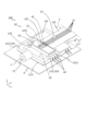
- FIG. 1 is a perspective view showing a wiring board according to an embodiment. 1 is a perspective view showing a wiring board and an optical module according to an embodiment;
- FIG. 3 is a plan view of the wiring board shown in FIG. 2 . 3 is a cross-sectional view of the wiring board shown in FIG. 2 taken along line III-III.
- 4 is a cross-sectional view taken along line IV-IV of the wiring board shown in FIG. 2.
- 4 is a cross-sectional view of a modified example of the wiring board shown in FIG. 2 taken along line IV-IV.
- FIG. 5 is an enlarged view of a main part A shown in FIG. 4 . 5 is an enlarged view of a modified example of the main part A shown in FIG. 4.
- FIG. 5 is an enlarged view of a main part B shown in FIG. 4 .
- 10A and 10B are diagrams showing modified examples of the organic resin substrate layer 12.
- FIG. 13 is a perspective view of a wiring board and an optical module according to another embodiment.
- 12 is a perspective view showing the wiring board and the optical module shown in FIG. 11 mounted on a printed circuit board.
- a wiring board in which a flexible wiring board is connected to a printed wiring board that uses an organic resin as a material there is known a wiring board in which a flexible wiring board is connected to a printed wiring board that uses an organic resin as a material, as in the invention described in Patent Document 1.
- Printed wiring boards and flexible wiring boards have a relatively low relative dielectric constant and are excellent in transmitting high-frequency signals.
- a semiconductor element that easily generates heat when driven such as a laser diode (LD) or a large scale integration (LSI)
- LSI large scale integration
- the printed wiring board may be mechanically or thermally deformed when it receives heat generated by the semiconductor element or receives an external impact.
- the printed wiring board may collide with the semiconductor element, causing damage to the semiconductor element.
- any direction of the wiring board may be the upper or lower direction, for convenience, an orthogonal coordinate system xyz is defined, and the positive side of the z direction is the upper direction.
- a plan view is a concept including a planar perspective view.
- the length, width, and thickness can be the dimension in the x direction, the dimension in the y direction, and the dimension in the z direction, respectively.
- a wiring board 10 includes a laminate 1 and a flexible wiring layer 2 .
- the laminate 1 has a ceramic substrate layer 11 and an organic resin substrate layer 12.
- the organic resin substrate layer 12 is located on the ceramic substrate layer 11.
- the material for the ceramic substrate layer 11 can be ceramics whose main component is at least one selected from the group consisting of aluminum oxide, silicon oxide, zirconium oxide, silicon carbide, silicon nitride, and aluminum nitride, or ceramics whose main component is a composite oxide such as mullite, zircon, steatite, enstatite, glass ceramics, and glass.
- the ceramic substrate layer 11 may be a single layer or may be a laminate of multiple layers.
- the ceramic substrate layer 11 is rectangular in plan view, with dimensions of 4 mm x 4 mm to 50 mm x 50 mm and a thickness of 0.01 mm to 10 mm.
- the outer shape of the ceramic substrate layer 11 may be the same as or different from the outer shape of the organic resin substrate layer 12.
- the ceramic substrate layer 11 may have a conductor located on the surface or inside.
- the material of the conductor include metal materials such as gold, silver, copper, nickel, tungsten, molybdenum, and manganese.
- the conductor may be formed by sintering a metal paste on the first intermediate surface 11s described later, or may be formed using a thin film formation technique such as a vapor deposition method or a sputtering method.
- the ceramic substrate layer 11 and the organic resin substrate layer 12 described below may be produced by additive manufacturing (AM) using a 3D printer. As shown in FIG. 9, the ceramic substrate layer 11 may have one or more protrusions 115 and/or depressions 116 at the interface with the organic resin substrate layer 12 .
- the organic resin substrate layer 12 is a portion mainly made of organic resin. Conductors such as vias and through holes may be located in the organic resin substrate layer 12.
- “mainly” refers to a state in which the volume ratio is 60% or more.
- the organic resin substrate layer 12 may contain a thermoplastic resin. In this case, an acrylic resin can be used as the thermoplastic resin.
- the proportion of the thermoplastic resin contained in the organic resin substrate layer 12 is preferably 1% by mass or more and 10% by mass or less. If the proportion of the thermoplastic resin contained in the organic resin substrate layer 12 is 1% by mass or more, the adhesiveness can be increased. If the proportion of the thermoplastic resin contained in the organic resin substrate layer 12 is 10% by mass or less, the possibility of deformation can be reduced.
- the organic resin substrate layer 12 may also contain an inorganic filler in addition to the organic resin.
- an inorganic filler in the organic resin substrate layer 12 By including an inorganic filler in the organic resin substrate layer 12, the mechanical strength of the organic resin substrate layer 12 can be increased.
- the thermal expansion coefficient of the organic resin substrate layer 12 can be reduced. When the thermal expansion coefficient of the organic resin substrate layer 12 is reduced, the difference in the thermal expansion coefficient between the organic resin of the organic resin substrate layer 12 and the conductor can be reduced. The stress generated at and near the interface between the organic resin and the conductor due to changes in the thermal expansion coefficient and Young's modulus can be reduced.
- the possibility of the ceramic substrate layer 11 and the organic resin substrate layer 12 peeling off due to the difference in thermal expansion coefficient can be reduced. This can improve the durability of the wiring board 10.
- organic resin one selected from the group consisting of epoxy resin, phenolic resin, unsaturated polyester resin, polytetrafluoroethylene resin, urea resin, melamine resin, thermosetting polyimide resin, etc. can be used.
- the protrusions 115 may penetrate into the organic resin substrate layer 12, or the organic resin substrate layer 12 may penetrate into the recesses 116. This can increase the bonding strength between the ceramic substrate layer 11 and the organic resin substrate layer 12. This state can also be expressed as the ceramic substrate layer 11 and the organic resin substrate layer 12 being bonded together.
- the flexible wiring layer 2 is located on or in the organic resin substrate layer 12. This state may be rephrased as the flexible wiring layer 2 being bonded to the organic resin substrate layer 12. A conductive bonding material such as solder may not be located between the flexible wiring layer 2 and the organic resin substrate layer 12.
- the ceramic substrate layer 11, which has higher rigidity than the organic resin substrate layer 12 is used, so that the mechanical and thermal deformation of the organic resin substrate layer 12 bonded to the flexible wiring layer 2 can be reduced. Therefore, when the first electronic component 51 is an optical semiconductor element such as a laser diode or a photodiode, the deviation of the optical axis can be reduced.
- the laminate 1 is less susceptible to mechanical damage caused by deformation of the entire laminate 1, even with the recent developments in large area and three-dimensional stacking. Furthermore, since the relative dielectric constants of the flexible wiring layer 2 and the organic resin base layer 12 are lower than that of the ceramic base layer 11, when transmitting a high-frequency signal in the wiring of the flexible wiring layer 2 (for example, the line conductor 21 described later), by moving the ceramic base layer 11 away from the wiring of the flexible wiring layer 2, the possibility of a decrease in the impedance value can be reduced. Therefore, it is possible to obtain a wiring board 10 that can efficiently transmit high-frequency signals.
- the flexible wiring layer 2 has flexibility. Note that, although FIG. 4 shows a case in which the flexible wiring layer 2 is partially exposed from the organic resin substrate layer 12, the entire flexible wiring layer 2 may be located within the organic resin substrate layer 12.
- the flexible wiring layer 2 may have an insulator 24, and a second conductor layer 22 and a line conductor 21 located on the surface of the insulator 24.
- the insulator 24 may have a second upper surface 22t.
- a resin film containing a resin material such as polyimide can be used as the insulator 24.
- the flexible wiring layer 2 may have a first portion 201 located within the organic resin substrate layer 12, and a second portion 202 exposed from the organic resin substrate layer 12. In other words, at least a portion of the flexible wiring layer 2 may be embedded within the organic resin substrate layer 12. This reduces the possibility that the flexible wiring layer 2 will be deformed and damaged. Note that, as shown in FIG. 8, when the flexible wiring layer 2 is embedded within the organic resin substrate layer 12, the second portion 202 may not be present.
- the organic resin base layer 12 may have a first side surface 121s and a second side surface 122s opposite to the first side surface 121s.
- the flexible wiring layer 2 may extend from the first side surface 121s toward the second side surface 122s.
- the flexible wiring layer 2 may also protrude from the second side surface 122s in a planar view.
- the flexible wiring layer 2 may extend in the positive direction of the x-axis.
- the first side surface 121s can be defined as the surface located on the side of the element mounting area 33 on which the first electronic component 51 is mounted. With this configuration, the flexible wiring layer 2 can be electrically connected to other electric circuits or electronic elements while reducing the possibility that the flexible wiring layer 2 will fall off, break, or bend on the side close to the first electronic component 51.
- the thermal conductivity of the ceramic substrate layer 11 may be greater than that of the organic resin substrate layer 12.
- the organic resin substrate layer 12 can efficiently transfer heat received from the first electronic component 51, such as a laser diode, to the ceramic substrate layer 11. This reduces the possibility of the wiring board 10 being damaged.
- the thermal conductivity of the organic resin substrate layer 12 may be greater than that of the flexible wiring layer 2. With this configuration, the heat received by the flexible wiring layer 2 can be efficiently transferred to the organic resin substrate layer 12, and then the heat received by the organic resin substrate layer 12 can be further transferred to the ceramic substrate layer 11.
- the thickness D11 of the ceramic substrate layer 11 may be greater than the thickness D12 of the organic resin substrate layer 12.
- This configuration can reduce the possibility of the organic resin substrate layer 12 deforming.
- the thermal conductivity of the ceramic substrate layer 11 is greater than the thermal conductivity of the organic resin substrate layer 12, the above configuration can efficiently diffuse heat, further reducing the possibility of damage to the wiring board 10.
- the thickness D2 of the flexible wiring layer 2 may be less than the thickness D12 of the organic resin substrate layer 12.
- the organic resin base layer 12 may have a fillet portion 12f.
- the fillet portion 12f is located from the second side surface 122s to the underside of the flexible wiring layer 2. This can improve the bonding strength between the flexible wiring layer 2 and the organic resin base layer 12.
- the fillet portion 12f may have a curved shape that is convex in the positive direction of the x-axis, or a curved shape that is convex in the negative direction of the x-axis.
- the organic resin base layer 12 may have a first upper surface 12t that is connected to the first side surface 121s and the second side surface 122s.
- the flexible wiring layer 2 may have a second upper surface 22t that is exposed from the organic resin base layer 12.
- the first upper surface 12t may have a portion that is flush with the second upper surface 22t. Therefore, compared to when the flexible wiring layer 2 is mounted on the organic resin base layer 12 by solder or the like, the amount of protrusion of the flexible wiring layer 2 in the z direction can be reduced, and the wiring board 10 can be made low-profile.
- the height of the flexible wiring layer 2 and the first electronic component 51 can be easily adjusted in the thickness direction (i.e., the z direction).
- the flexible wiring layer 2 may have a fourth side surface 24s that connects to the second upper surface 22t.
- the organic resin base material layer 12 may cover at least a portion of the fourth side surface 24s in a cross-sectional view.
- the bonding strength between the organic resin base material layer 12 and the flexible wiring layer 2 can be further increased.
- the anchor effect of the organic resin base material layer 12 on the flexible wiring layer 2 can be increased.
- the fourth side surface 24s may have a curved shape that is convex in the width direction of the flexible wiring layer 2 in a cross-sectional view.
- the line conductor 21 may be coated with an insulating material.
- a second electronic component 52 may be connected to the line conductor 21, for example, as shown in FIG. 2 or FIG. 21.
- the second electronic component 52 may be, for example, an electric circuit element such as a capacitor, an inductor, a resistor, a noise reduction filter, or a chip bead, or may be an integrated circuit (IC).
- IC integrated circuit
- the flexible wiring layer 2 may have a third side surface 23s.
- the first side surface 121s and the third side surface 23s may be flush with each other. This allows the flexible wiring layer 2 to be supported by the organic resin base layer 12 up to the end.
- the flexible wiring layer 2 can be brought as close as possible to the element mounting area 33 or the first electronic component 51.
- the line conductor 21 of the flexible wiring layer 2 and the first electronic component 51 are electrically connected by a wire 41, the length of the wire 41 can be shortened by adopting the above configuration. Therefore, high-frequency signals can be stably transmitted in the flexible wiring layer 2.
- the third side surface 23s can be defined as the surface of the flexible wiring layer 2 that faces the element mounting area 33 or the first electronic component 51.
- the organic resin substrate layer 12 may have a film-like first conductor layer 121.
- the flexible wiring layer 2 may have a film-like second conductor layer 22.
- the first conductor layer 121 and the second conductor layer 22 may be in surface contact. With this configuration, the first conductor layer 121 and the second conductor layer 22 are in contact with each other at their film surfaces, and the two layers are restrained by each other. This reduces the possibility that the organic resin substrate layer 12 and the flexible wiring layer 2 may be deformed. More specifically, the first conductor layer 121 and the second conductor layer 22 may each have unevenness on their surfaces, and the unevenness formed on the first conductor layer 121 and the second conductor layer 22 may fit together and be in contact with each other.
- the first penetrating conductor 431 is exposed from the first upper surface 12t.
- the first penetrating conductor 431 may be electrically connected to the first electronic component 51 and/or the second electronic component 52.
- the first penetrating conductor 431 may be used as a conductor for passing a low-frequency AC signal or a DC signal, or may be used as a grounding conductor.
- the first penetrating conductor 431 may be spaced from the flexible wiring layer 2. This configuration reduces the possibility that the first penetrating conductor 431 will be distorted or broken when the flexible wiring layer 2 is bonded to the organic resin base material layer 12. Furthermore, the first penetrating conductor 431 may be partially exposed on the side surface of the laminate 1.
- the wiring board 10 may further include a second penetrating conductor 432 that penetrates the laminate 1 and the flexible wiring layer 2 in the z-direction.
- the second penetrating conductor 432 may be electrically connected to any of the line conductors 21.
- the second penetrating conductor 432 may be electrically connected to the first electronic component 51 and/or the second electronic component 52.
- the second penetrating conductor 432 may also be used as a conductor for passing a low-frequency AC signal or DC signal, or as a conductor for grounding.
- the wiring board 10 may further have a pedestal portion 110.
- the pedestal portion 110 may be a member that supports the first electronic component 51, and may be a separate body from the laminate 1.
- the pedestal portion 110 may be, for example, a thermoelectric cooler (TEC: ThermoElectric Cooler) such as a Peltier element, or may be a laminate of a metal material or a ceramic material.
- TEC thermoelectric cooler
- the first electronic component 51 can be mounted directly or indirectly on the pedestal portion 110.
- the pedestal portion 110 may be integral with the ceramic substrate layer 11. That is, the ceramic substrate layer 11 may have the pedestal portion 110. In this case, the pedestal portion 110 may protrude from the fourth side surface 14s. This state may be rephrased as the pedestal portion 110 being connected to the fourth side surface 14s.
- the pedestal portion 110 has a first pedestal surface 110s on which the ceramic substrate layer 11 is exposed in a planar view.
- the first electronic component 51 can be mounted directly or indirectly on the first pedestal surface 110s.
- the ceramic substrate layer 11 may also have a first intermediate surface 11s.
- the first intermediate surface 11s is a surface that overlaps with the organic resin substrate layer 12 in a planar view and is in contact with the organic resin substrate layer 12 in a cross-sectional view.
- the first pedestal surface 110s may be located above the first intermediate surface 11s (i.e., in the positive direction in the x-axis direction).
- This configuration allows the first seat surface 110s to be closer to the second upper surface 22t, so that, for example, when connecting the flexible wiring layer 2 and the first electronic component 51 mounted on the first seat surface 110s with a wire 41, the length of the wire 41 can be shortened. This reduces the possibility that the impedance value will fluctuate in the flexible wiring layer 2, for example, when transmitting a high-frequency signal.
- the ceramic substrate layer 11 may have a shelf portion 112 protruding from the fourth side surface 14s.
- the shelf portion 112 has a third upper surface 112t.
- An electrode 1121 may be located on the third upper surface 112t.
- the electrode 1121 may be used as a conductor for passing a low-frequency AC signal or a DC signal, or may be used as a grounding conductor.
- the material 1121 of the electrode may be, for example, a metal material such as gold, silver, copper, nickel, tungsten, molybdenum, or manganese. Since the electrode 1121 is located around the element mounting area 33, the distance between the first electronic component 51 mounted on the element mounting area 33 and the electrode 1121 can be shortened. This allows the wiring board 10 to be miniaturized.
- the electrode 1121 may extend through the ceramic substrate layer 11 to the lower surface of the ceramic substrate layer 11.
- the shelf portion 112 may protrude from a position on the fourth side surface 14s that is different from the pedestal portion 110. Furthermore, the shelf portion 112 may be shaped to surround the element mounting area 33 in a plan view. In other words, the area surrounded by the shelf portion 112 can be defined as the element mounting area 33.
- the wiring board 10 may further include a substrate 3 bonded to the ceramic substrate layer 11.
- the substrate 3 may be integrally formed with the ceramic substrate layer 11.
- the material of the substrate 3 may be ceramic.
- the substrate 3 may be a metal plate 31 having a metal material. That is, the wiring board 10 may further include a metal plate 31 bonded to the ceramic substrate layer 11.
- the metal plate 31 may have an element mounting area 33.
- the first electronic component 51 can be mounted or mounted directly or indirectly in the element mounting area 33. With the above configuration, heat generated by the first electronic component 51 can be efficiently dissipated by the metal plate 31.
- the wiring board 10 may have one or more lead terminals 42 electrically connected to the ceramic substrate layer 11. By having the lead terminals 42, it is possible to electrically connect to wiring of the printed circuit board 6 described later.
- the lead terminals 42 may be bonded to the side of the ceramic substrate layer 11 or to the bottom surface of the ceramic substrate layer 11.
- the wiring board 10 may have solder balls bonded to the bottom surface of the ceramic substrate layer 11. In this case, the wiring board 10 can be connected in a so-called BGA (Ball Grid Array) manner.
- the wiring board 10 may further include a pair of differential signal lines 21p.
- the pair of differential signal lines 21p is located on at least one of the flexible wiring layers 2.
- the organic resin base layer 12 may have a first upper surface 12t and a first recess 12o.
- the first upper surface 12t is connected to the first side surface 121s and the second side surface 122s.
- the first recess 12o may open to the first upper surface 12t. In a plan view, the first recess 12o may be located between the pair of differential signal lines 21p.
- the first recess 12o is filled with at least one of a dielectric material such as air, a resin material, or a glass material, and has a lower dielectric constant than the organic resin base layer 12. Therefore, the possibility of a decrease in the characteristic impedance of the pair of differential signal lines 21p when transmitting a high-frequency signal can be reduced.
- the first recess 12o may extend to the first side surface 121s.
- the ceramic substrate layer 11 may also have a second recess 11o.
- the second recess 11o may be located between the pair of differential signal lines 21p.
- the second recess 11o may overlap the first recess 12o.
- the second recess 11o is also filled with at least one dielectric material such as a resin material or a glass material, and has a lower dielectric constant than the ceramic substrate layer 11. This reduces the possibility that the characteristic impedance of the pair of differential signal lines 21p will decrease when transmitting a high-frequency signal.
- the second recess 11o may extend to the fourth side surface 14s.
- the ceramic substrate layer 11 may be in the form of an unfired green sheet or in the form after firing.
- the ceramic substrate layer 11 may have a protrusion 115 or a depression 116 formed in advance on the first intermediate surface 11s under predetermined conditions.
- Sandblasting and etching can be used as a method for forming the protrusion 115 or the depression 116 on the first intermediate surface 11s.
- alkaline etching as an etching condition, it becomes easier to form the protrusion 115 or the depression 116 on the first intermediate surface 11s.
- the first through conductor 431 and the second through conductor 432 may be formed in the ceramic substrate layer 11 by forming a through hole in the ceramic substrate layer 11 in advance and filling the through hole with a conductive paste.
- an uncured layer of the organic resin substrate layer 12 is prepared by forming a conductor (which may include a first through conductor 431 and a second through conductor 432) in a resin material.
- a conductor which may include a first through conductor 431 and a second through conductor 432
- through holes are formed at predetermined positions in the resin insulation layers. The through holes are formed by punching or laser processing.
- conductors are formed in the through holes.
- the through conductors are formed by a conductive paste or plating.
- wiring may be formed on the surface of the organic resin substrate layer 12 (the surface facing the first upper surface 12t and/or the first intermediate surface 11s). This wiring can also be formed by a conductive paste or plating.
- the flexible wiring layer 2 is pressed against the organic resin base layer 12. If the flexible wiring layer 2 is to be embedded in the organic resin base layer 12, a resin insulating layer may be further laminated on the flexible wiring layer 2.
- the unfired laminate 1 is pressurized and heated under specified conditions to produce a fired laminate 1.
- the wiring board 10 can be obtained by dicing or other processes into a specified shape.
- the optical module 100 includes a wiring board 10 and one or more first electronic components 51 electrically connected to the flexible wiring layer 2.
- the first electronic components 51 is an optical semiconductor element.
- the optical semiconductor element may be, for example, a laser diode (LD), a photodiode (PD), a vertical cavity surface emitting laser (VCSEL), or an LED that emits near-infrared light, visible light, or ultraviolet light.
- the first electronic components 51 may be a transimpedance amplifier (TIA: Transimpedance Amplifier). Also, when one of the first electronic components 51 is a photodiode, the transimpedance amplifier may be electrically connected to the photodiode, and the flexible wiring layer 2 may be electrically connected to the transimpedance amplifier.
- TIA Transimpedance Amplifier
- the first electronic component 51 may be located in the element mounting area 33. In one embodiment, when the ceramic substrate layer 11 has a shelf portion 112 as shown in Figures 2 and 3, the first electronic component 51 is surrounded by the shelf portion 112.
- the first electronic component 51 is mounted directly or indirectly on the element mounting area 33.
- the first electronic component 51 may be located on the base 110 and/or the submount 32.
- the wiring pattern 321 may be located on the submount 32.
- the line conductor 21 and the wiring pattern 321 are connected by a wire 41.
- the wiring pattern 321 may be connected to the first electronic component 51 (optical semiconductor element) by a bonding wire.
- the wiring pattern 321 may extend to below the first electronic component 51 (optical semiconductor element), in which case the first electronic component 51 may be mounted on the wiring pattern 321 by a conductive paste such as solder.
- the optical module 100 may be mounted on a printed circuit board 6. Wiring is formed on the printed circuit board 6, and for example, the lead terminals 42 described above may be electrically connected to the wiring on the printed circuit board 6.
- the printed circuit board 6 may be a PCB (Printed Circuit Board).
- the optical module 100 may further include an optical component 7.
- the optical component 7 may have, for example, a lens or an optical fiber.
- the optical component 7 may have a first light-transmitting portion 71.
- the first light-transmitting portion 71 is a through-hole that passes through the optical component 7, and a lens or glass may be fixed inside the first light-transmitting portion 71.
- An optical fiber may be inserted into the first light-transmitting portion 71.
- the optical component 7 may be attached to the ceramic substrate layer 11, more specifically, to the shelf portion 112.
- the optical module 100 can be used as an optical communication module.
- the optical module 100 can also be used for LiDAR (Light Detection and Ranging).
- the ceramic substrate layer 11 may further include a wall portion 113 protruding from the ceramic substrate layer 11 in the z-direction and a connection pad 1131 located on the wall portion 113.
- the surface on which the connection pad 1131 is located may be located above the first upper surface 12t (in the positive direction of the z-axis) in a cross-sectional view.
- the material of the connection pad 1131 may be, for example, a metal material such as gold, silver, copper, nickel, tungsten, molybdenum, and manganese.
- the connection pad 1131 may be electrically connected to the wiring, the first through conductor 431, and the second through conductor 432 located in the ceramic substrate layer 11.
- the connection pad 1131 may also be electrically connected to the first electronic component 51 and/or the second electronic component 52.
- a frame body 8 may be attached to the wall portion 113.
- the material of the frame body 8 may be, for example, a ceramic material or a metal material.
- the frame body 8 may be made of the same material as the wall portion 113, in which case the wall portion 113 and the frame body 8 may be integrally formed.
- the area surrounded by the frame body 8 and the ceramic substrate layer 11 may be defined as the element mounting area 33.
- the wall portion 113 may be located on the printed circuit board 6.
- the connection pad 1131 may be electrically connected to the printed circuit board 6.
- the printed circuit board 6 is located above the ceramic substrate layer 11, not below it.
- the first electronic component 51 and the second electronic component 52 are covered by the wiring board 10 including the ceramic substrate layer 11 and the printed circuit board 6. This reduces the possibility that the first electronic component 51 and/or the second electronic component 52, such as an optical semiconductor element, will be damaged by external factors.
- a metal plate 31 may be located on the underside (negative direction of the z-axis) of the ceramic substrate layer 11. In the wiring board 10 and optical module 100 according to other embodiments shown in Figures 21 and 22, by positioning the metal plate 31 as described above, heat dissipation can be improved.
- This disclosure can be used as a wiring board and an optical module using the wiring board.
Landscapes
- Physics & Mathematics (AREA)
- Engineering & Computer Science (AREA)
- Microelectronics & Electronic Packaging (AREA)
- Condensed Matter Physics & Semiconductors (AREA)
- General Physics & Mathematics (AREA)
- Electromagnetism (AREA)
- Optics & Photonics (AREA)
- Manufacturing & Machinery (AREA)
- Structure Of Printed Boards (AREA)
Priority Applications (1)
| Application Number | Priority Date | Filing Date | Title |
|---|---|---|---|
| JP2025503850A JPWO2024181322A1 (https=) | 2023-02-27 | 2024-02-22 |
Applications Claiming Priority (2)
| Application Number | Priority Date | Filing Date | Title |
|---|---|---|---|
| JP2023028599 | 2023-02-27 | ||
| JP2023-028599 | 2023-02-27 |
Publications (1)
| Publication Number | Publication Date |
|---|---|
| WO2024181322A1 true WO2024181322A1 (ja) | 2024-09-06 |
Family
ID=92590538
Family Applications (1)
| Application Number | Title | Priority Date | Filing Date |
|---|---|---|---|
| PCT/JP2024/006627 Ceased WO2024181322A1 (ja) | 2023-02-27 | 2024-02-22 | 配線基板および配線基板を用いた光モジュール |
Country Status (2)
| Country | Link |
|---|---|
| JP (1) | JPWO2024181322A1 (https=) |
| WO (1) | WO2024181322A1 (https=) |
Citations (6)
| Publication number | Priority date | Publication date | Assignee | Title |
|---|---|---|---|---|
| JP2000340917A (ja) * | 1999-05-26 | 2000-12-08 | Fujitsu Ltd | 複合モジュール及びプリント回路基板ユニット |
| JP2009105204A (ja) * | 2007-10-23 | 2009-05-14 | Sony Chemical & Information Device Corp | 配線基板の受台及びこれを用いた配線基板の接続装置、接続方法 |
| JP2011155091A (ja) * | 2010-01-27 | 2011-08-11 | Opnext Japan Inc | 光モジュール |
| JP2013149692A (ja) * | 2012-01-18 | 2013-08-01 | Nec Corp | シリコンインターポーザ及びそれを用いる半導体装置 |
| JP2021036592A (ja) * | 2017-09-11 | 2021-03-04 | Ngkエレクトロデバイス株式会社 | 配線基板とフレキシブル基板の接続構造および電子部品収納用パッケージ |
| JP2022168758A (ja) * | 2021-04-26 | 2022-11-08 | キヤノン株式会社 | フレキシブル配線板、モジュール、及び電子機器 |
-
2024
- 2024-02-22 WO PCT/JP2024/006627 patent/WO2024181322A1/ja not_active Ceased
- 2024-02-22 JP JP2025503850A patent/JPWO2024181322A1/ja active Pending
Patent Citations (6)
| Publication number | Priority date | Publication date | Assignee | Title |
|---|---|---|---|---|
| JP2000340917A (ja) * | 1999-05-26 | 2000-12-08 | Fujitsu Ltd | 複合モジュール及びプリント回路基板ユニット |
| JP2009105204A (ja) * | 2007-10-23 | 2009-05-14 | Sony Chemical & Information Device Corp | 配線基板の受台及びこれを用いた配線基板の接続装置、接続方法 |
| JP2011155091A (ja) * | 2010-01-27 | 2011-08-11 | Opnext Japan Inc | 光モジュール |
| JP2013149692A (ja) * | 2012-01-18 | 2013-08-01 | Nec Corp | シリコンインターポーザ及びそれを用いる半導体装置 |
| JP2021036592A (ja) * | 2017-09-11 | 2021-03-04 | Ngkエレクトロデバイス株式会社 | 配線基板とフレキシブル基板の接続構造および電子部品収納用パッケージ |
| JP2022168758A (ja) * | 2021-04-26 | 2022-11-08 | キヤノン株式会社 | フレキシブル配線板、モジュール、及び電子機器 |
Also Published As
| Publication number | Publication date |
|---|---|
| JPWO2024181322A1 (https=) | 2024-09-06 |
Similar Documents
| Publication | Publication Date | Title |
|---|---|---|
| CN101447541A (zh) | 半导体器件 | |
| CN102077372A (zh) | 发光器件封装及其制造方法 | |
| CN105359632B (zh) | 布线基板以及电子装置 | |
| TWI605280B (zh) | Electronic module | |
| CN1630069B (zh) | 装载光学元件用组件及其制造方法 | |
| CN104126224B (zh) | 元件收纳用封装件 | |
| CN115117727A (zh) | 光模块 | |
| KR20150046235A (ko) | 전기 소자 어셈블리 | |
| CN101835343A (zh) | 印刷布线板、包含其的印刷集成电路板及其制造方法 | |
| CN110140205A (zh) | 半导体装置 | |
| JP2004288937A (ja) | 発光素子収納用パッケージおよび発光装置 | |
| US7816690B2 (en) | Light-emitting device | |
| JP7545349B2 (ja) | 光モジュール | |
| WO2020175626A1 (ja) | 電子素子搭載用パッケージ及び電子装置 | |
| JP3320932B2 (ja) | チップパッケージ実装体、及びチップパッケージが実装される回路基板、並びに回路基板の形成方法 | |
| WO2024181322A1 (ja) | 配線基板および配線基板を用いた光モジュール | |
| JP6626735B2 (ja) | 電子部品搭載用基板、電子装置および電子モジュール | |
| JP7753380B2 (ja) | 電子素子実装用基板、電子装置、および電子モジュール | |
| CN113690729A (zh) | 一种封装结构及光模块 | |
| JP5302177B2 (ja) | 光導波路基板および光電気混載装置 | |
| KR20040063784A (ko) | 반도체장치 | |
| US7417292B2 (en) | Arrangement for connecting the terminal contacts of an optoelectronic component to a printed circuit board | |
| JP2007287767A (ja) | 光サブアセンブリ | |
| JPH10173083A (ja) | 電子部品搭載用配線基板とその製造方法 | |
| WO2021006344A1 (ja) | アレイアンテナ装置 |
Legal Events
| Date | Code | Title | Description |
|---|---|---|---|
| 121 | Ep: the epo has been informed by wipo that ep was designated in this application |
Ref document number: 24763802 Country of ref document: EP Kind code of ref document: A1 |
|
| ENP | Entry into the national phase |
Ref document number: 2025503850 Country of ref document: JP Kind code of ref document: A |
|
| WWE | Wipo information: entry into national phase |
Ref document number: 2025503850 Country of ref document: JP |
|
| NENP | Non-entry into the national phase |
Ref country code: DE |
|
| 122 | Ep: pct application non-entry in european phase |
Ref document number: 24763802 Country of ref document: EP Kind code of ref document: A1 |