WO2024166256A1 - 画像転送システムおよび画像転送方法 - Google Patents
画像転送システムおよび画像転送方法 Download PDFInfo
- Publication number
- WO2024166256A1 WO2024166256A1 PCT/JP2023/004197 JP2023004197W WO2024166256A1 WO 2024166256 A1 WO2024166256 A1 WO 2024166256A1 JP 2023004197 W JP2023004197 W JP 2023004197W WO 2024166256 A1 WO2024166256 A1 WO 2024166256A1
- Authority
- WO
- WIPO (PCT)
- Prior art keywords
- image
- area
- data
- image data
- necessary
- Prior art date
- Legal status (The legal status is an assumption and is not a legal conclusion. Google has not performed a legal analysis and makes no representation as to the accuracy of the status listed.)
- Ceased
Links
Images




Classifications
-
- G—PHYSICS
- G01—MEASURING; TESTING
- G01B—MEASURING LENGTH, THICKNESS OR SIMILAR LINEAR DIMENSIONS; MEASURING ANGLES; MEASURING AREAS; MEASURING IRREGULARITIES OF SURFACES OR CONTOURS
- G01B11/00—Measuring arrangements characterised by the use of optical techniques
- G01B11/24—Measuring arrangements characterised by the use of optical techniques for measuring contours or curvatures
-
- G—PHYSICS
- G01—MEASURING; TESTING
- G01B—MEASURING LENGTH, THICKNESS OR SIMILAR LINEAR DIMENSIONS; MEASURING ANGLES; MEASURING AREAS; MEASURING IRREGULARITIES OF SURFACES OR CONTOURS
- G01B11/00—Measuring arrangements characterised by the use of optical techniques
- G01B11/24—Measuring arrangements characterised by the use of optical techniques for measuring contours or curvatures
- G01B11/25—Measuring arrangements characterised by the use of optical techniques for measuring contours or curvatures by projecting a pattern, e.g. one or more lines, moiré fringes on the object
-
- H—ELECTRICITY
- H04—ELECTRIC COMMUNICATION TECHNIQUE
- H04N—PICTORIAL COMMUNICATION, e.g. TELEVISION
- H04N13/00—Stereoscopic video systems; Multi-view video systems; Details thereof
- H04N13/20—Image signal generators
- H04N13/204—Image signal generators using stereoscopic image cameras
- H04N13/254—Image signal generators using stereoscopic image cameras in combination with electromagnetic radiation sources for illuminating objects
-
- H—ELECTRICITY
- H04—ELECTRIC COMMUNICATION TECHNIQUE
- H04N—PICTORIAL COMMUNICATION, e.g. TELEVISION
- H04N7/00—Television systems
- H04N7/18—Closed-circuit television [CCTV] systems, i.e. systems in which the video signal is not broadcast
Definitions
- the present invention relates to an image transfer system and method for transferring image data from an imaging device that captures an image of a workpiece illuminated with a line of light to an image processing device.
- a line of light may be irradiated onto a workpiece and its image captured.
- a line of light is irradiated onto the workpiece while it is moved relative to the measurement optical system, and an image is then captured, and the workpiece height is determined from the captured image using the principles of triangulation.
- Patent Document 1 discloses a device that appropriately sets the ROI (Region of Interest) that determines the pixel readout range of the image sensor, thereby preventing the capture of images from areas that are not useful for measurement and reducing the size of the image data being transferred.
- the ROI area is made, the smaller the measurement range of the height measurement becomes.
- the only way to expand the measurement range is to make the ROI area larger, and in the end, the size of the image data cannot be significantly reduced.
- the object of the present invention is to provide an image transfer system and method that can reduce the size of image data as much as possible when transferring the image data from an imaging device that captures an image of a workpiece illuminated with a line of light to an image processing device.
- An image transfer system includes a light source that irradiates a line light onto a workpiece moving relatively in a predetermined feed direction, an imaging device that captures an image of the workpiece and its surroundings irradiated with the line light, an image processing device that performs required image processing on image data captured by the imaging device, and a transfer device that transfers the image data to the image processing device through an interface, and the transfer device executes a process of detecting an illuminated area in the image data where reflected light of the line light is observed, and a process of distinguishing between an area of a predetermined width including the illuminated area as a necessary area and an area other than the necessary area as an unnecessary area, and transfers the image data of the necessary area to the image processing device.
- An image transfer method is an image transfer method in which a line light is irradiated onto a workpiece while the workpiece is moved relatively in a predetermined feed direction, and an image of the workpiece and its surroundings irradiated with the line light is captured, and the image data obtained is transferred to an external device through an interface.
- an irradiated area in which reflected light of the line light is observed is detected, an area of a predetermined width including the irradiated area is determined as a necessary area, and areas other than the necessary area are clearly distinguished as unnecessary areas, and the image data of the necessary area is transferred to the external device.
- FIG. 1 is a schematic diagram showing in a simplified manner the hardware configuration of an image transfer system according to an embodiment of the present invention.
- 2A to 2C are schematic diagrams showing a method for measuring the height of a part (workpiece) by the light-section method.
- FIG. 3 is a flowchart showing an image transfer method according to a comparative example.
- FIG. 4 is a schematic diagram for explaining the problem with the image transfer method of the comparative example.
- FIG. 5 is a schematic diagram for explaining the image transfer method of the present invention.
- FIG. 6A is a diagram showing an example of an image acquired by the light section method
- FIG. 6B is a diagram for explaining an unnecessary region of the image.
- FIG. 7 is a flowchart showing an image transfer method according to an embodiment of the present invention.
- FIG. 8A to 8C are diagrams showing examples of reduction in image data to be transferred.
- FIG. 9 is a block diagram showing the functional configuration of the image transfer system.
- FIG. 10 is a schematic diagram showing a first embodiment of the process for distinguishing between necessary and unnecessary areas in a pixel line.
- FIG. 11 is a schematic diagram showing a second embodiment of the process for distinguishing between necessary and unnecessary areas in a pixel line.
- FIG. 12 is a schematic diagram showing a third embodiment of the process for distinguishing between necessary and unnecessary areas in a pixel line.
- FIG. 13 is a diagram showing an example of processing when a plurality of candidates for line light are detected.
- 14A and 14B are diagrams showing another example of processing when a plurality of candidates for line light are detected.
- FIG. 15 is a diagram showing another example of processing when a plurality of candidates for line light are detected.
- FIG. 16 is a diagram showing an example of processing when the line of light does not fit within the number of pixels of the extraction area.
- the image transfer system and image transfer method according to the present invention can be applied to various devices that capture images of various workpieces, such as various industrial products, semi-finished products, machine parts, electronic parts, food, and agricultural products, by irradiating them with a line of light for the purpose of measurement, etc., and perform the required image processing on the captured image.
- various workpieces such as various industrial products, semi-finished products, machine parts, electronic parts, food, and agricultural products, by irradiating them with a line of light for the purpose of measurement, etc., and perform the required image processing on the captured image.
- one preferred application of the present invention is to measure the height of a component mounted on a board using the light section method as the workpiece.
- a measurement device that measures the height of a component using the light section method will be assumed and described.
- the measurement device is, for example, an appearance inspection machine that is incorporated into a mounting board production line where electronic components are mounted on printed circuit boards, and that inspects whether the electronic components are mounted on the printed circuit board
- [Device configuration] 1 is a schematic diagram showing a simplified hardware configuration of an image transfer system 1 according to this embodiment.
- the image transfer system 1 includes a camera unit 2, an image processing device 3, and a transmission cable 4 (interface).
- the camera unit 2 captures an image of a part C as a workpiece, and transfers the acquired image data to the image processing device 3.
- the image processing device 3 performs required image processing on the transferred image data.
- the transmission cable 4 connects the camera unit 2 and the image processing device 3 so that they can communicate electrically.
- a Camera Link cable that realizes image data transfer in accordance with the Camera Link standard (Note: Camera Link is a registered trademark of the AIA) can be used.
- the camera unit 2 includes a line light source 21 (light source), a camera 22 (imaging device), and a transfer device 23.
- the line light source 21 irradiates a line light SL onto the part C.
- the line light SL is light that extends linearly in one direction.
- the line light source 21 can be a light source device including a laser light source and an optical component that converts the laser light emitted by the laser light source into slit light that spreads in a fan shape.
- the part C is moved relatively in a predetermined scanning direction F (predetermined feed direction) by a moving mechanism (not shown). Therefore, the line light source 21 irradiates a line light SL onto the part C moving in the scanning direction F.
- the camera 22 captures an image of the component C illuminated with the line light SL and its surroundings. That is, the camera 22 captures a partial image of the component C including the reflected light RL of the line light SL.
- the imaging optical axis of the camera 22 is vertical, while the projection axis of the line light SL emitted from the line light source 21 is set in an oblique direction. These axial arrangements are arranged for measuring the three-dimensional shape of the component C by the light-section method.
- the camera 22 includes an imaging lens 24 and an imaging sensor 25.
- the imaging lens 24 forms an optical image including the reflected light RL on the light receiving surface of the imaging sensor 25.
- the imaging sensor 25 is a solid-state imaging element such as a CMOS sensor or a CCD sensor, and photoelectrically converts the optical image into image data.
- the transfer device 23 transfers the image data acquired by the camera 22 to the image processing device 3 via the transmission cable 4.
- an image signal including a synchronization signal and image data is transferred using a fixed amount (e.g., 28 bits) of binary signal synchronized with a reference clock.
- the transfer device 23 does not transfer all of the image data acquired by the camera 22, but deletes unnecessary areas of the image data before transferring it.
- the image processing device 3 executes image processing to obtain height data of the part C by the light section method based on the image data of the part C acquired by the camera unit 2.
- FIG. 1 an example is shown in which two camera units 2 are connected to the image processing device 3. There may be one camera unit 2, or three or more.
- the transmission cable 4 connecting the camera unit 2 and the image processing device 3 transmits image signals, for example, by the LVDS (Low Voltage Differential Signaling) transmission method.
- LVDS Low Voltage Differential Signaling
- the measurement target here is, as shown in FIG. 2(A), a component C (workpiece) mounted on the surface PS of a substrate P.
- the camera 22 of the camera unit 2 has an imaging optical axis AX that extends in a direction perpendicular to the surface PS, and captures an image of the component C.
- the line light source 21 has a projection optical axis that has a predetermined intersection angle ⁇ with the imaging optical axis AX, and emits a line light SL along the projection optical axis.
- the line light SL is irradiated onto the component C that is the measurement target.
- Figure 2 (B) shows an image IM captured by camera 22 at a certain scan position SC1 where a line light SL is irradiated onto component C.
- camera 22 captures reflected light RL1 from surface PS of substrate P around component C and reflected light RL2 from the top surface of component C.
- reflected light RL1 and RL2 are observed at different X coordinate positions on image IM. Specifically, reflected light RL1 appears at coordinate x11, and reflected light RL2 appears at coordinate x12, which is downstream in the scanning direction from coordinate x11.
- the three-dimensional shape data of part C can be obtained by integrating multiple height data acquired by scanning.
- the height data acquired at one scan position SC1, SC2, SC3 is based on the result of reflected light RL1, RL2 being irradiated at different X coordinate positions. For this reason, when integrating the data, a height table is created that matches, for example, the height data at coordinate x12 obtained in the area of part C at scan position SC1 with the height data at coordinate x12 obtained in the area of surface PS at the subsequent scan position.
- [Description of Comparative Example] 3 is a flowchart showing an image transfer process by the image transfer system 1 according to the comparative example.
- the camera 22 of the camera unit 2 performs an operation of capturing an image of a component C as an object to be captured (step S1).
- This image capturing operation includes irradiating the component C with a line light SL from the line light source 21 and capturing an optical image including reflected light RL from the surface PS of the substrate P around the component C by the image capturing sensor 25.
- the image data (brightness data) photoelectrically converted by the image capturing sensor 25 is swept out to the transfer device 23 at a predetermined frame rate (fps: Frames Per Second) (step S2).
- the frame rate is an index that determines the image capturing speed of the camera 22.
- the image data is output from the transfer device 23 to the image processing device 3 (step S3).
- the transfer device 23 In data transfer conforming to the Camera Link standard, the transfer device 23 generates transmission data for an image signal including a synchronization signal and image data, and transmits the image signal via the transmission cable 4 using the LVDS transmission method.
- the image signal is received by the image input circuit of the image processing device 3 (step S4).
- the image processing device 3 uses the principles previously described in Figures 2(B) and (C), the image processing device 3 performs the required image processing on the transferred image signal to obtain height data of the component C (step S5).
- the image processing device 3 identifies the reflected light RL1, RL2 of the line light SL1, SL2 as exemplified in Figure 2(B) on the image data, and derives the height data of the component C by referring to the coordinate values of the reflected light RL1, RL2.
- the transfer speed of the transmission cable 4 which is the interface between the camera unit 2 and the image processing device 3, may not be able to keep up with the increased frame rate of the image sensor 25.
- the transfer speed of the transmission cable 4 becomes a bottleneck, preventing the performance of the image sensor 25 from being fully utilized, and as a result, there are cases where it is not possible to increase the speed of height measurement.
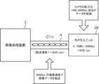
- FIG. 4 is a schematic diagram for explaining the problems with the image transfer method of the comparative example.
- FIG. 4 shows an example in which a first camera unit 2A and a second camera unit 2B are connected to an image processing device 3 via a transmission cable 4 with a transfer speed of 1.0 GB/sec.
- the image sensor 25 provided in the first camera unit 2A has the ability to output a 1 MB size frame image at 1000 fps per second. In other words, the first camera unit 2A can output image data at 1.0 GB/sec.
- the image sensor 25 provided in the second camera unit 2B has the ability to output a 1 MB size frame image at 2000 fps per second, and can output image data at 2.0 GB/sec.
- the transmission cable 4 can keep up with the output rate (1.0 GB/sec) from the first camera unit 2A, but cannot keep up with the output rate (2.0 GB/sec) of the second camera unit 2B.
- the second camera unit 2B has an imaging speed of 1 MB/2000 fps
- the transfer speed limit of the transmission cable 4 causes a problem in which it can only transfer at 1 MB/1000 fps.
- FIG. 5 is a schematic diagram outlining the image transfer method of this embodiment. Shown here are the second camera unit 2B, image processing device 3, and transmission cable 4 shown in FIG. 4. As described above, the second camera unit 2B has an imaging speed of 1MB/2000fps. In this embodiment, the image data size is reduced in the transfer device 23 to match the transfer speed of the transmission cable 4 while maintaining the imaging speed of the second camera unit 2B.
- the transfer device 23 executes a process to reduce the data size of a frame image obtained from one image capture by the second camera unit 2B from 1 MB to 0.5 MB.
- the image data to be reduced is the image data of the unnecessary area mentioned above.
- the second camera unit 2B is utilized as an imaging device that outputs 0.5 MB size frame images at 2000 fps per second. This makes the output rate of the second camera unit 2B 1.0 GB/sec, which can match the transfer rate of the transmission cable 4. Therefore, the imaging speed capability of the second camera unit 2B of "2000 fps" can be effectively utilized, contributing to faster processing.
- Fig. 6(A) is a diagram showing image 5 of one frame acquired during height measurement using the light section method. This image 5 corresponds to image IM previously shown in Fig. 2(B).
- Image 5 consists of an illuminated area 51 where reflected light RL of the line light SL is observed, and a dark area 52 where reflected light RL is not observed.
- Illuminated area 51 is a rectangular area that is long in the X direction, which is the extension direction of the line light SL.
- illuminated area 51 is observed at a position corresponding to reflected light RL1 from the periphery of part C and reflected light RL2 from the top surface of part C.
- FIG. 6(B) is a diagram for explaining the unnecessary area 53 of image 5.
- image 5 what is necessary for height measurement using the light-section method is the irradiation area 51 of the line light SL and its adjacent areas, and the remaining areas are not used for height measurement.
- the necessary area used for height measurement is the area of image 5 with the minimum Y-direction width that allows one and the other ends of the Y-direction width of the irradiation area 51 (the upper and lower ends in FIG. 6) to be determined.
- the area of image 5 other than the necessary area becomes the unnecessary area 53.
- the position information (coordinate values) of the irradiation area 51 or the necessary area in image 5 is specified, the area of image 5 other than the necessary area can be treated as the unnecessary area 53 that is not used.
- the transfer device 23 Since image data corresponding to the unnecessary area 53 will not actually be used even if it is transferred to the image processing device 3, the transfer itself may be omitted. Therefore, by having the transfer device 23 transfer only the image data of the necessary area to the image processing device 3 and discarding the image data of the unnecessary area 53, it is possible to suppress the size of the image data to be transferred to the minimum necessary.
- FIG. 7 is a flowchart showing an example of an image transfer method according to this embodiment.
- the processes in steps S1, S2, S3, S4, and S5 are similar to steps S1 to S5 in the comparative example described above based on the flowchart in FIG. 3.
- the difference from the comparative example is that between step S2, in which image data is discharged from the imaging sensor 25, and step S3, in which an image signal is output from the transfer device 23, the transfer device 23 executes a process of reducing the amount of image data to be transferred (step S10).
- the transfer device 23 executes a process of detecting the illuminated area 51 where the reflected light RL of the line light SL is observed in the image data output from the imaging sensor 25 in step S2 (step S11), and a process of distinguishing between a region of a predetermined width including the illuminated area 51 as a necessary area and an unnecessary area 53 outside the necessary area (step S12). In the following step S3, the transfer device 23 transfers only the image data of the necessary area to the image processing device 3.
- FIGS. 8(A) to (C) are diagrams showing an example of the process of reducing the amount of image data to be transferred.
- Image 5 shown in FIG. 8(A) uses image 5 previously shown in FIG. 6(B).
- step S11 the luminance value of each pixel is evaluated for each pixel line in image 5 in the Y direction perpendicular to the extension direction of irradiation area 51 of line light SL, thereby obtaining position information on irradiation area 51 on image 5, i.e., coordinate values.
- coordinate values Several specific examples of how to evaluate the luminance value are given below.
- an area of a predetermined width in the Y direction of image 5 including the illuminated area 51 detected in step S11 is identified as the necessary area A1.
- the necessary area A1 is typically set to include the illuminated area 51 and adjacent areas of a predetermined width in the Y direction that sandwich the illuminated area 51.
- an image in which the illuminated area 51 is sandwiched between a pair of adjacent areas in the Y direction becomes the image of the necessary area A1.
- Such an image of the necessary area A1 has the advantage that it becomes easier to accurately determine the position information of the illuminated area 51 based on the brightness contrast between the illuminated area 51, which is a bright area, and the adjacent areas, which are dark areas.
- the unnecessary area 53 is set above and below the necessary area A1.
- the width in the XY direction of the unnecessary area 53 depends on the XY position of the irradiation area 51. For example, in the part of the irradiation area 51 observed in the center of the Y direction of the image 5, the upper unnecessary area 53 has a narrow width in the Y direction, and the lower unnecessary area 53 has a relatively wide width in the Y direction.
- the irradiation area 51 in the center of the Y direction is observed as an arc shape in the image 5.
- the upper and lower unnecessary areas 53 are not rectangular as in FIG. 8(A), but the upper unnecessary area 53 has an arc-shaped depression, and the lower unnecessary area 53 has an arc-shaped bulge.
- FIG. 8(B) shows a schematic diagram of an image transferred from the transfer device 23 to the image processing device 3.
- the transferred image is only the image corresponding to the necessary area A1 of the entire image 5.
- the size of the image data to be transferred can be reduced to approximately 1/10.
- the coordinate values of the irradiation area 51 of the line light SL or the necessary area A1 are attached to the necessary area A1 as data indicating the positional information of the necessary area A1. These coordinate values are used by the image processing device 3 as information indicating the position in the Y direction of the image 5 from which the necessary area A1 was cut out.
- FIG. 8(C) is a diagram showing a schematic diagram of the image signal D transferred from the transfer device 23 to the image processing device 3 after the processing of steps S11 and S12.
- the image signal D includes brightness data d1 to d5 of the pixels constituting the image of the necessary area A1 as image data da, and coordinate data D1 indicating the coordinate values of the illumination area 51 or the necessary area A1.
- the coordinate data D1 is data in which the coordinate values are replaced with brightness data selected from 0 to 255. For example, 1 to 4 pixel bits are allocated to the transfer of the coordinate data D1.
- the position information of the irradiation area 51 or the necessary area A1 can be transferred using the bits of the channel that transfers the image data da, so there is no need to secure a separate channel or interface for transferring the position information.
- [Image transfer system configuration] 9 is a block diagram showing the configuration of an image transfer system 1 applied to the height measurement of a part C.
- the image transfer system 1 includes a camera unit 2 including a line light source 21, a camera 22, and a transfer device 23, and an image processing device 3.
- the transfer device 23 and the image processing device 3 are electrically connected to each other via a transmission cable 4.
- a Camera Link cable is used as the transmission cable 4, and both are connected to each other so as to be able to perform LVDS communication.
- an interface based on a data transfer standard other than the Camera Link standard for example, CoaXPress or USB 3.0, may be adopted.
- an example is shown in which the transfer device 23 transfers data based on the Camera Link standard.
- the camera 22 captures an image of the part C moving relatively in the scanning direction F under the illumination of the line light SL emitted by the line light source 21.
- the transfer device 23 has a function of outputting an image signal including a synchronization signal and image data acquired by the camera 22, using a certain amount of binary signal synchronized with a reference clock.
- the transfer device 23 transfers the image signal to the image processing device 3 via the transmission cable 4.
- the transfer device 23 functionally includes an image input circuit 26, an irradiation area specification unit 27, a necessary area setting unit 28, and an image output circuit 29.
- the image input circuit 26 accepts image data output at a predetermined frame rate from the imaging sensor 25 (FIG. 1) of the camera 22.
- the image input circuit 26 also generates a synchronization signal based on the Camera Link standard, and places brightness data as image data in a predetermined number of data bits per reference clock period.
- the irradiation area identification unit 27 performs a predetermined process on the image data of the image 5 shown in FIG. 8A, and performs the process of detecting the irradiation area 51 shown in step S11 of FIG. 7. As shown in FIG. 8C, the coordinate values of the detected irradiation area 51 are converted into luminance data and incorporated into the vacant bits of the data bits in which the image data is arranged.
- the necessary area setting unit 28 executes the discrimination process shown in step S12.
- the necessary area setting unit 28 discriminates an area of a predetermined width including the irradiation area 51 as a necessary area A1 and the area other than the necessary area A1 as an unnecessary area 53, and performs a process of discarding the image data of the unnecessary area 53.
- the image output circuit 29 converts the synchronization signal and the image signal including the image data and coordinate value data corresponding to the necessary area A1 into a signal capable of LVDS communication and outputs it.
- the image processing device 3 comprises an image input circuit 31, an image memory 32, an image processing unit 33, and a height calculation unit 34.
- the image input circuit 31 is a deserializer circuit for LVDS communication, and receives a synchronization signal and an image signal transferred from the transfer device 23.
- the image memory 32 temporarily stores the transferred image signal.
- the image processing unit 33 accesses the image memory 32 at appropriate times, and performs processing to identify the position of the irradiation area 51 corresponding to the line light SL.
- the height calculation unit 34 executes processing to obtain height data of the component C by the light section method, based on the positional relationship of the multiple irradiation areas 51 identified on the image 5.
- First Example 10 is a schematic diagram showing a first embodiment of a process for distinguishing between a necessary area A1 and an unnecessary area 53 in one pixel line GL.
- This distinguishing process is also a process for detecting an irradiation area 51 of the line light SL included in an image 5, the majority of which is occupied by a dark area 52.
- the process for detecting the irradiation area 51 executed by the irradiation area specifying unit 27 is performed sequentially for each pixel line GL in the Y direction.
- the pixel line GL is a pixel line in a direction perpendicular to the extension direction (X direction) of the line light SL. This point is the same in the second and third embodiments described later.
- the pixel line GL includes a dark portion 52 with a relatively small luminance value and an illuminated area 51 consisting of a bright portion with a luminance value that is clearly greater than that of the dark portion 52.
- the line light SL is a long and narrow light extending in the X direction, and therefore usually appears in a narrow width at one point on one pixel line GL.
- an extraction area SA is set that is composed of N pixels and has a fixed extraction width that is narrower than the Y direction width of the pixel line GL. In the first embodiment, this extraction area SA determines the necessary area A1.
- the illuminated area specification unit 27 performs a calculation to determine the total value of the luminance data of the pixels present in the extraction area SA while shifting the extraction area SA along the pixel line GL.
- the range in which the extraction area SA is shifted is the range from the start to the end of the pixel line GL.
- the extraction area SA is shifted one pixel at a time from the top to the bottom of the pixel line GL, while processing is performed to find the total value of the luminance data of the pixels present within the extraction area SA. Then, the position of the illumination area 51 is detected based on the position on the pixel line GL of the extraction area SA where the total value is maximized.
- the extraction area SA does not include the illuminated area 51 and covers only the dark area 52, so the total value of the luminance data is a small value.
- the extraction area SA approaches part of the illuminated area 51. For this reason, the total value is larger at position (b) than at position (a).
- the extraction area SA includes all of the illuminated area 51.
- the total value of the luminance data at position (c) is larger than positions (a) and (b) and indicates the maximum value. From this result, it can be detected that the illuminated area 51 is present within the extraction area SA at position (c).
- position (c) is the position where the total value of the luminance data is maximum
- the illumination area 51 is detected by setting an extraction area SA equivalent to the Y-direction width of the necessary area A1. Therefore, once detection of the illumination area 51 is complete, the necessary area A1 is automatically identified. Therefore, the necessary area setting unit 28 extracts the extraction area SA at position (c) as the necessary area A1, and treats the area other than this necessary area A1 as the unnecessary area 53.
- Second Example 11 is a schematic diagram showing a second embodiment of the discrimination process.
- the position of the illumination region 51 is identified by detecting the position of maximum brightness for each pixel line GL. That is, the illumination region identification unit 27 checks the brightness values of the pixels constituting one pixel line GL, and detects the position of the maximum pixel where the brightness value is maximum.
- the line light SL does not have a uniform light intensity within its width in the Y direction, but has a light intensity with a Gaussian distribution. For this reason, the center of the irradiation area 51 in the Y direction is generally the brightest. Therefore, by detecting the position of the maximum pixel, the center position of the irradiation area 51 in the Y direction can be obtained, and as a result, the irradiation area 51 can be detected. Note that if multiple maximum pixels are detected consecutively in the Y direction, the center of those pixel rows in the Y direction can be treated as the center coordinate value of the irradiation area 51.
- the necessary area setting unit 28 specifies a predetermined width centered on the position of the maximum pixel as the necessary area A1. For example, N pixels corresponding to the Y direction width of the necessary area A1 are determined in advance, and an area of N pixels centered on the position of the maximum pixel is specified as the necessary area A1. Naturally, the width of N pixels is narrower than the Y direction width of the pixel line GL. This number of N pixels may be the same as the N pixels that define the extraction area SA in the first embodiment. A detailed example of setting the number of N pixels will be explained later.
- the necessary area setting unit 28 extracts the necessary area A1 identified above as the data area to be transferred, and treats the area other than the necessary area A1 as the unnecessary area 53.
- the upper end or lower end of the identified necessary area A1 is set as the coordinate data of the necessary area A1.
- the image data output from the image output circuit 29 is the brightness data of the illuminated area 51 and the dark area 52 in the necessary area A1, and the position data obtained by converting the coordinate data into brightness data.
- the coordinate data may be placed either on the start side (upper side in the figure) or the end side (lower side) of the image data of the necessary area A1.
- the position coordinates of the illuminated area 51 are identified by simply detecting the maximum value of the brightness data for each pixel line GL, so that the detection process of the illuminated area 51 can be simplified.
- ⁇ Third Example> 12 is a schematic diagram showing a third embodiment of the discrimination process.
- each pixel line GL is divided into a high luminance portion and a low luminance portion, and the position of the irradiation region 51 is specified based on the position of the maximum high luminance portion that has the maximum width along the pixel line GL among the observed high luminance portions.
- the irradiation area specifying unit 27 checks the luminance value of each pixel constituting the pixel line GL, and binarizes it into high luminance parts 51A, 51B and low luminance part 52A using a predetermined threshold. Depending on the degree of threshold setting or when light from other light sources enters, multiple high luminance parts 51A, 51B may be detected, as shown in FIG. 12. In anticipation of such a case, the irradiation area specifying unit 27 refers to the binarized area.
- the irradiation area specifying unit 27 specifies the area of the maximum high luminance part 51A, which has the largest Y-direction width along the pixel line GL, as the irradiation area 51. Furthermore, the necessary area setting unit 28 specifies the width of N pixels centered on the center position of the maximum high luminance part 51A in the Y direction as the necessary area A1.
- the necessary area setting unit 28 extracts the necessary area A1 identified above as the data area to be transferred, and performs processing to distinguish areas other than this necessary area A1 from the unnecessary area 53.
- the upper or lower end of the identified necessary area A1 is set as the coordinate data of the necessary area A1.
- the image data output from the image output circuit 29 is the luminance data of the illuminated area 51 and dark areas 52 within the necessary area A1, and position data obtained by converting the coordinate data into luminance data.
- the luminance data to be transferred is the data before being subjected to binarization processing.
- the illuminated area 51 can be accurately identified through the processes of binarization of high-luminance and low-luminance areas, evaluation of the Y-direction width of the high-luminance area, and identification of the position of the maximum high-luminance area.
- FIG. 13 is a diagram showing an example of manual selection and setting when multiple candidates for the irradiation area 51 of the line light SL are detected.
- FIG. 13(A) for example, assume that the execution of the discrimination process based on the luminance values in the first to third embodiments described above results in three line light candidates 51a, 51b, and 51c being detected on one pixel line GL, and the remaining part being a dark area 52.
- the starting point of the pixel line GL is the top of the figure, and the brightness values of the pixels are checked from the top to the bottom.
- the three line light candidates 51a, 51b, 51c are detected in the order of 51a ⁇ 51b ⁇ 51c.
- manual selection setting as shown in FIG. 13(B), it is set in advance that the first detected line light candidate 51a is selected as the illumination area 51.
- FIG. 13(C) it is set in advance that the last detected line light candidate 51c is selected as the illumination area 51.
- Such manual setting can simplify the selection process when multiple candidates for the illumination area 51 are detected.
- the multiple candidates for the illumination area 51 it is also possible to set the multiple candidates for the illumination area 51 to be easily detected.
- the first embodiment assuming that a position on the pixel line GL where the sum of the luminance data of the extraction area SA is the maximum value M1 is detected, other positions of the extraction area SA where the sum of the luminance data falls within the range of (maximum value M1 - coefficient R) are also included and are considered as candidates for the illumination area 51.
- the coefficient R is a value that is arbitrarily set by the user based on experience, etc., or a value that is set as a predetermined ratio to the maximum value M1.
- one illuminated area 51 is identified by applying the above-mentioned manual selection setting or the next-mentioned automatic selection setting method.
- the positions of other pixels where the luminance value falls within the range of (maximum value M2 - coefficient R) are also determined as candidates for the illuminated area 51.
- the positions of other high-luminance parts where the binarized area falls within the range of (maximum value M3 - coefficient R) are also determined as candidates for the illuminated area 51.
- FIGS. 14(A) and (B) are diagrams showing examples of automatic selection settings when multiple candidates for the irradiation area 51 of the line light SL are detected.
- FIG. 14(A) shows an example of referring to the results of pixel lines adjacent to the detection target of the irradiation area 51.
- FIG. 14(A) shows an example in which two line light candidates 51a and 51b are detected in the pixel line GL of the detection target. In this case, the identification result of the irradiation area 51 in the pixel line GLa adjacent to the pixel line GL in the same image is referred to. Then, of the two line light candidates 51a and 51b, the one closer to the irradiation area 51 of the adjacent pixel line GLa is automatically selected.
- the line light candidate 51b closer to the irradiation area 51 of the adjacent pixel line GLa is selected as the irradiation area 51.
- FIG. 14(B) shows an example where the results of the previous imaging, which are sequentially imaged by the light-section method, are referenced.
- FIG. 14(B) also shows an example where two line light candidates 51a, 51b are detected in the pixel line GL to be detected.
- the result of identifying the irradiation area 51 in the same pixel line GLb as the pixel line GL to be detected in the image acquired in the previous imaging is referenced.
- the two line light candidates 51a, 51b the one closer to the irradiation area 51 of the adjacent pixel line GLb is automatically selected.
- the line light candidate 51a closer to the irradiation area 51 of the adjacent pixel line GLb is selected as the irradiation area 51.
- Process B described above is a method for detecting the illumination area 51 of a pixel line GL using another discrimination process when multiple candidates for the illumination area 51 are detected for one pixel line GL using one discrimination process. Specifically, when multiple candidates are detected using any one of the algorithms of the first to third embodiments of the discrimination process for the necessary area A1 in one pixel line GL illustrated in Figures 10 to 12, a process for detecting the illumination area 51 is executed again using the algorithm of another embodiment.
- the process of detecting the illumination area 51 for that pixel line GL is executed again using the discrimination process using the second embodiment in FIG. 11 or the third embodiment in FIG. 12. If multiple candidates for the illumination area 51 are still detected in the second discrimination process, the above-mentioned manual selection setting or automatic selection setting method is applied to identify one illumination area 51.
- Process C described above is a method of transferring image data in which multiple illumination areas 51 have been detected to the image processing device 3 as is, and entrusting processing to the image processing device 3.
- (A) and (B) of FIG. 15 assume that two line light candidates 51a, 51b have been detected on one pixel line GL.
- the illumination area 51 and the necessary area A1 for that pixel line GL are not identified, that is, no data reduction processing is performed, and the image data of pixels of the full image width A2 is transferred as is.
- coordinate data 54 shows an example in which coordinate data 54 is placed at the start end of image data of full image width A2.
- Figure 15(B) shows an example in which coordinate data 54 is placed at the end end of image data of full image width A2.
- coordinate data 54 is placed next to image data for N pixels from the top end of pixel line GL.
- the number of pixels N (see Figures 10 to 12) that determines the Y-direction width of the necessary area A1 in the pixel line GL may be set arbitrarily by the user, or may be automatically set based on predetermined setting criteria.
- the transfer device 23 refers to the maximum frame rate of the imaging sensor 25 equipped in the camera 22 and the maximum transfer speed of the transmission cable 4 (interface). Then, the number of pixels that will make the size of the data to be transferred equal to or smaller than the transfer size determined by the maximum transfer speed is calculated, and this number of pixels is set as N pixels that determine the width of the necessary area A1.
- N pixels that determine the width of the necessary area A1.
- the transfer device 23 automatically measures the difference between the maximum frame rate of the image sensor 25 and the maximum transfer speed of the transmission cable 4, and performs a process of determining the optimal value of N.
- the above process can be performed by the following steps 1 to 4.
- ⁇ Step 1> The exposure time and ROI of the image sensor 25 of the camera 22 are set to conditions suitable for imaging the component C by the light section method.
- the width of the image determined by the setting of the ROI is W
- the height of the image is H. Note that H corresponds to the width of the pixel line GL in the Y direction.
- ⁇ Step 2> Calculate the maximum frame rate FPS of the image sensor 25 when the camera 22 captures an image under the conditions of step 1 above.
- ⁇ Step 3> Find the coefficient AN that makes the data size per second smaller than the transfer size Cs determined by the maximum transfer speed of the transmission cable 4 when imaging is performed at the FPS found in step 2. At this time, the number of data bits Da for arranging the coordinate data of the necessary area A1 is also taken into consideration.
- the judgment process can be performed by detecting the length of the shift position where the total brightness data value of the extraction area SA is V% of the maximum brightness data total value detected in the pixel line GL.
- the value of V is a threshold value set appropriately by the user. If the shift position of the extraction area SA where the total brightness data value is V% or more is observed continuously for N pixels or more, it is judged that the irradiation area 51 does not fall within the necessary area A1. In the case of the second embodiment (FIG. 11), if pixels having a brightness value of V% of the maximum brightness value are observed continuously for N pixels or more, it is judged that the irradiation area 51 does not fall within the necessary area A1. In the case of the third embodiment (FIG. 12), if the Y-direction width of the maximum high brightness part 51A exceeds N pixels, it is judged that the irradiation area 51 does not fall within the necessary area A1.
- FIG. 16 shows an example in which a line light candidate 51n having a width greater than N pixels has been detected in one pixel line GL.
- any luminance data is placed in the data bits A1n for the image data in the transferred data.
- luminance data with a luminance value of 0 or random luminance data is placed in the data bits A1n.
- unique data in which the error code has been converted into luminance data is placed as the coordinate data 54. In this way, by transferring the image data with an error code attached, it becomes possible for the image processing device 3 to perform appropriate post-processing.
- the transfer device 23 determines that the irradiation area 51 does not fall within the required area A1, it is desirable to have the transfer device 23 carry out appropriate countermeasures. For example, the transfer device 23 is caused to carry out a process to automatically expand the number of pixels (N) that defines the required area A1 from the next image capture. The number of pixels in the area with a value equal to or greater than V% detected in the above determination process may be set as a new N value. By carrying out such countermeasures, the relationship between the irradiation area 51 and the required area A1 can be optimized, and the position of the irradiation area 51 can be accurately identified.
- An image transfer system includes a light source that irradiates a line light onto a workpiece moving relatively in a predetermined feed direction, an imaging device that captures an image of the workpiece and its surroundings irradiated with the line light, an image processing device that performs required image processing on image data captured by the imaging device, and a transfer device that transfers the image data to the image processing device through an interface, and the transfer device executes a process of detecting an illuminated area in the image data where reflected light of the line light is observed, and a process of distinguishing between an area of a predetermined width including the illuminated area as a necessary area and an area other than the necessary area as an unnecessary area, and transfers the image data of the necessary area to the image processing device.
- An image transfer method is an image transfer method in which a line light is irradiated onto a workpiece while the workpiece is moved relatively in a predetermined feed direction, and an image of the workpiece and its surroundings irradiated with the line light is captured, and the image data obtained is transferred to an external device through an interface.
- an irradiated area in which reflected light of the line light is observed is detected, an area of a predetermined width including the irradiated area is determined as a necessary area, and areas other than the necessary area are clearly distinguished as unnecessary areas, and the image data of the necessary area is transferred to the external device.
- the illuminated area of the line light is detected in the acquired image data, and a clear distinction is made between a necessary area including the illuminated area and other unnecessary areas. Then, only the image data of the necessary area is transferred to the image processing device or external device. In other words, instead of restricting the imaging range from the beginning as with an ROI, the necessary area is identified and transferred for each acquired image data. As a result, image data essential for image processing for measurement, etc. is transferred to the image processing device, while image data for unnecessary areas is not transferred and is essentially discarded. Therefore, the image data size can be kept to a minimum, and high-speed transfer of required image data can be achieved even when it is not possible to increase the image data transfer speed of the interface.
- the image processing device performs image processing to obtain height data of the workpiece using a light section method.
- the necessary area is set to include the illuminated area and an adjacent area of a predetermined width that sandwiches the illuminated area.
- the image of the illuminated area sandwiched between the adjacent areas becomes the image of the required area.
- the transfer device transfers the luminance data of the pixels constituting the image of the required area as the image data, and replaces the position information of the illuminated area or the required area with the luminance data before transferring it.
- position information of the illuminated area or required area that is, information on which coordinate area on the image senses the line light
- position information of the illuminated area or required area can be transferred using the bits of a channel that transfers brightness data as image data, so there is no need to secure a separate channel or interface for transferring the position information.
- the process of detecting the illuminated area executed by the transfer device may include a process of setting a fixed extraction width narrower than the width of the pixel line in the direction perpendicular to the extension direction of the line light of the image data, executing a calculation to obtain the sum of the luminance data of the pixel group present within the extraction width while shifting the extraction width in the range from the start end to the end end of the pixel line, and identifying the position coordinates of the illuminated area based on the position on the pixel line of the extraction width where the sum is maximum.
- the total luminance data of the pixels within the extraction width is calculated while shifting the extraction width, so the position of the illuminated area can be reliably detected from the image data.
- the transfer device may detect the illumination area by detecting brightness data of pixels constituting a pixel line in a direction perpendicular to the extension direction of the line light of the image data, and identify the position coordinates of the illumination area based on the position of the maximum pixel where the brightness data value is maximum, and may identify a predetermined width centered on the maximum pixel as the required area as the discrimination process.
- the position coordinates of the illuminated area are identified by simply detecting the maximum value of the luminance data for each pixel line, which simplifies the process of identifying the illuminated area.
- the transfer device may perform the process of detecting the illuminated area by binarizing the brightness data of the pixels constituting a pixel line in a direction perpendicular to the extension direction of the line light of the image data into high brightness and low brightness areas using a predetermined threshold value, specifying the position coordinates of the illuminated area based on the position of the maximum high brightness area among the high brightness areas that has the maximum width along the pixel line, and performing the process of distinguishing between the two by specifying a predetermined width centered on the central position of the maximum high brightness area as the required area.
- the illuminated area can be accurately identified through the process of binarizing the high-luminance and low-luminance areas, evaluating the width of the high-luminance areas, and identifying the position of the maximum high-luminance area.
- the transfer device when multiple candidates for the irradiation area are detected on one pixel line, it is desirable for the transfer device to perform one of the following processes: select one of the irradiation areas using a predetermined selection process, re-execute the process of detecting the irradiation area, or transfer the image data in which multiple irradiation areas are detected as is.
- the line light is a single linear light, but in actual processing, multiple areas that meet the requirements for an irradiation area may be detected. According to the above aspect, when multiple irradiation areas are detected, it is possible to execute the appropriate next-stage processing.
- the transfer device may execute a process for determining whether the projection area of the image data is within the predetermined required area, and if the projection area is not within the required area, may attach an error code to the image data and transfer it to the image processing device.
- image data is transferred with an error code attached, allowing the image processing device to perform appropriate processing.
- the transfer device determines that the projection area does not fall within the required area, it is desirable to execute a process to expand the required area. This makes it possible to optimize the relationship between the projection area and the required area, and to accurately identify the position of the projection area.
- the transfer device may set the width of the required area by referring to the maximum frame rate of the imaging sensor of the imaging device and the maximum transfer speed of the interface, and determining the number of pixels that will make the size of the data to be transferred equal to or smaller than the transfer size determined by the maximum transfer speed.
- a necessary area having a number of pixels that allows high-speed transfer of image data can be set, taking into account the maximum frame rate of the image sensor and the maximum transfer speed of the interface.
Landscapes
- Physics & Mathematics (AREA)
- Engineering & Computer Science (AREA)
- Multimedia (AREA)
- Signal Processing (AREA)
- General Physics & Mathematics (AREA)
- Electromagnetism (AREA)
- Computer Vision & Pattern Recognition (AREA)
- Length Measuring Devices By Optical Means (AREA)
- Optical Communication System (AREA)
Priority Applications (5)
| Application Number | Priority Date | Filing Date | Title |
|---|---|---|---|
| CN202380093561.8A CN120641720A (zh) | 2023-02-08 | 2023-02-08 | 图像传输系统及图像传输方法 |
| PCT/JP2023/004197 WO2024166256A1 (ja) | 2023-02-08 | 2023-02-08 | 画像転送システムおよび画像転送方法 |
| KR1020257025545A KR20250130651A (ko) | 2023-02-08 | 2023-02-08 | 화상 전송 시스템 및 화상 전송 방법 |
| JP2024575953A JP7838130B2 (ja) | 2023-02-08 | 2023-02-08 | 画像転送システムおよび画像転送方法 |
| TW112130899A TWI860043B (zh) | 2023-02-08 | 2023-08-17 | 圖像傳送系統及圖像傳送方法 |
Applications Claiming Priority (1)
| Application Number | Priority Date | Filing Date | Title |
|---|---|---|---|
| PCT/JP2023/004197 WO2024166256A1 (ja) | 2023-02-08 | 2023-02-08 | 画像転送システムおよび画像転送方法 |
Publications (1)
| Publication Number | Publication Date |
|---|---|
| WO2024166256A1 true WO2024166256A1 (ja) | 2024-08-15 |
Family
ID=92262206
Family Applications (1)
| Application Number | Title | Priority Date | Filing Date |
|---|---|---|---|
| PCT/JP2023/004197 Ceased WO2024166256A1 (ja) | 2023-02-08 | 2023-02-08 | 画像転送システムおよび画像転送方法 |
Country Status (5)
| Country | Link |
|---|---|
| JP (1) | JP7838130B2 (https=) |
| KR (1) | KR20250130651A (https=) |
| CN (1) | CN120641720A (https=) |
| TW (1) | TWI860043B (https=) |
| WO (1) | WO2024166256A1 (https=) |
Citations (5)
| Publication number | Priority date | Publication date | Assignee | Title |
|---|---|---|---|---|
| JPS63149507A (ja) * | 1986-12-13 | 1988-06-22 | Kobe Steel Ltd | 作業線自動検出方法 |
| JP2001116528A (ja) * | 1999-08-10 | 2001-04-27 | Fuji Mach Mfg Co Ltd | 3次元データ取得方法および3次元データ取得装置 |
| JP2001188008A (ja) * | 1999-12-28 | 2001-07-10 | Yasunaga Corp | 高さ測定装置 |
| JP2012220473A (ja) * | 2011-04-14 | 2012-11-12 | Yaskawa Electric Corp | 3次元形状計測装置およびロボットシステム |
| WO2014057580A1 (ja) * | 2012-10-12 | 2014-04-17 | 株式会社ニレコ | 形状計測方法及び形状計測装置 |
Family Cites Families (6)
| Publication number | Priority date | Publication date | Assignee | Title |
|---|---|---|---|---|
| JP2000275024A (ja) | 1999-03-25 | 2000-10-06 | Minolta Co Ltd | 3次元入力装置 |
| JP6415454B2 (ja) * | 2013-01-25 | 2018-10-31 | テレダイン・イノバシオネス・ミクロエレクトロニカス・ソシエダッド・リミターダ・ユニパーソナルTeledyne Innovaciones Microelectronicas,Slu | 画像センサ用の高度の関心領域機能 |
| CN107923737B (zh) * | 2015-12-13 | 2019-12-17 | 富通尼奥有限责任公司 | 用于超像素调制和环境光抑制的方法和设备 |
| JP2019095376A (ja) * | 2017-11-27 | 2019-06-20 | 倉敷紡績株式会社 | 画像処理システム |
| JP7594539B2 (ja) * | 2019-09-26 | 2024-12-04 | 株式会社小糸製作所 | ゲーティングカメラ、自動車、車両用灯具、画像処理装置、画像処理方法 |
| CN114419011B (zh) * | 2022-01-24 | 2025-04-22 | 郑州轻工业大学 | 一种棉花异性纤维在线检测方法及系统 |
-
2023
- 2023-02-08 KR KR1020257025545A patent/KR20250130651A/ko active Pending
- 2023-02-08 WO PCT/JP2023/004197 patent/WO2024166256A1/ja not_active Ceased
- 2023-02-08 CN CN202380093561.8A patent/CN120641720A/zh active Pending
- 2023-02-08 JP JP2024575953A patent/JP7838130B2/ja active Active
- 2023-08-17 TW TW112130899A patent/TWI860043B/zh active
Patent Citations (5)
| Publication number | Priority date | Publication date | Assignee | Title |
|---|---|---|---|---|
| JPS63149507A (ja) * | 1986-12-13 | 1988-06-22 | Kobe Steel Ltd | 作業線自動検出方法 |
| JP2001116528A (ja) * | 1999-08-10 | 2001-04-27 | Fuji Mach Mfg Co Ltd | 3次元データ取得方法および3次元データ取得装置 |
| JP2001188008A (ja) * | 1999-12-28 | 2001-07-10 | Yasunaga Corp | 高さ測定装置 |
| JP2012220473A (ja) * | 2011-04-14 | 2012-11-12 | Yaskawa Electric Corp | 3次元形状計測装置およびロボットシステム |
| WO2014057580A1 (ja) * | 2012-10-12 | 2014-04-17 | 株式会社ニレコ | 形状計測方法及び形状計測装置 |
Also Published As
| Publication number | Publication date |
|---|---|
| TWI860043B (zh) | 2024-10-21 |
| TW202433011A (zh) | 2024-08-16 |
| JPWO2024166256A1 (https=) | 2024-08-15 |
| CN120641720A (zh) | 2025-09-12 |
| JP7838130B2 (ja) | 2026-03-31 |
| KR20250130651A (ko) | 2025-09-02 |
Similar Documents
| Publication | Publication Date | Title |
|---|---|---|
| JPH0572961B2 (https=) | ||
| US20100289891A1 (en) | Apparatus for inspecting object under inspection | |
| JP4434417B2 (ja) | プリント配線板の検査装置 | |
| KR20130141345A (ko) | 땜납 높이 검출 방법 및 땜납 높이 검출 장치 | |
| KR102798445B1 (ko) | 2d 이미지 데이터를 획득하고 광 삼각 측량으로부터의 3d 이미지 데이터와 관련시키기 위한 방법 및 배열체 | |
| JP3871944B2 (ja) | 外観検査装置 | |
| JP2007078540A (ja) | 外観検査方法及び外観検査装置 | |
| WO2024166256A1 (ja) | 画像転送システムおよび画像転送方法 | |
| KR20090121612A (ko) | 골판지 품질 불량 자동 검사 방법 및 장치 | |
| JPS63273047A (ja) | 凹凸状態検出装置 | |
| JP2003156451A (ja) | 欠陥検出装置 | |
| JP4549838B2 (ja) | 光沢度測定方法および装置 | |
| JP4821647B2 (ja) | 電子部品の端子位置検出方法 | |
| JP4967132B2 (ja) | 対象物表面の欠陥検査方法 | |
| JP2818347B2 (ja) | 外観検査装置 | |
| JP4613090B2 (ja) | 検査装置 | |
| JPH04104044A (ja) | 半田ペーストの印刷状態検査装置 | |
| JP4792314B2 (ja) | 基板検査装置および基板検査方法 | |
| KR100705643B1 (ko) | 반도체 소자의 검사 방법 | |
| JP5402182B2 (ja) | 外観検査方法及び外観検査装置 | |
| JPH0814546B2 (ja) | 光学式形状検査装置 | |
| JP2006078421A (ja) | パターン欠陥検出装置及びその方法 | |
| JP2019095238A (ja) | 画像処理システム、画像処理方法、及びプログラム | |
| JPH0618239A (ja) | クリーム半田印刷検査装置 | |
| JP2017181270A (ja) | 検査方法及び検査装置 |
Legal Events
| Date | Code | Title | Description |
|---|---|---|---|
| 121 | Ep: the epo has been informed by wipo that ep was designated in this application |
Ref document number: 23920299 Country of ref document: EP Kind code of ref document: A1 |
|
| WWE | Wipo information: entry into national phase |
Ref document number: 2024575953 Country of ref document: JP |
|
| ENP | Entry into the national phase |
Ref document number: 1020257025545 Country of ref document: KR Free format text: ST27 STATUS EVENT CODE: A-0-1-A10-A15-NAP-PA0105 (AS PROVIDED BY THE NATIONAL OFFICE) |
|
| WWE | Wipo information: entry into national phase |
Ref document number: 202380093561.8 Country of ref document: CN |
|
| NENP | Non-entry into the national phase |
Ref country code: DE |
|
| WWP | Wipo information: published in national office |
Ref document number: 202380093561.8 Country of ref document: CN |
|
| 122 | Ep: pct application non-entry in european phase |
Ref document number: 23920299 Country of ref document: EP Kind code of ref document: A1 |