WO2024150769A1 - 配線形成用部材、配線層の形成方法、及び、配線形成部材 - Google Patents
配線形成用部材、配線層の形成方法、及び、配線形成部材 Download PDFInfo
- Publication number
- WO2024150769A1 WO2024150769A1 PCT/JP2024/000316 JP2024000316W WO2024150769A1 WO 2024150769 A1 WO2024150769 A1 WO 2024150769A1 JP 2024000316 W JP2024000316 W JP 2024000316W WO 2024150769 A1 WO2024150769 A1 WO 2024150769A1
- Authority
- WO
- WIPO (PCT)
- Prior art keywords
- wiring
- adhesive layer
- layer
- conductive particles
- forming member
- Prior art date
- Legal status (The legal status is an assumption and is not a legal conclusion. Google has not performed a legal analysis and makes no representation as to the accuracy of the status listed.)
- Ceased
Links
Images





Classifications
-
- H—ELECTRICITY
- H05—ELECTRIC TECHNIQUES NOT OTHERWISE PROVIDED FOR
- H05K—PRINTED CIRCUITS; CASINGS OR CONSTRUCTIONAL DETAILS OF ELECTRIC APPARATUS; MANUFACTURE OF ASSEMBLAGES OF ELECTRICAL COMPONENTS
- H05K3/00—Apparatus or processes for manufacturing printed circuits
- H05K3/46—Manufacturing multilayer circuits
- H05K3/4644—Manufacturing multilayer circuits by building the multilayer layer by layer, i.e. build-up multilayer circuits
- H05K3/4652—Adding a circuit layer by laminating a metal foil or a preformed metal foil pattern
- H05K3/4655—Adding a circuit layer by laminating a metal foil or a preformed metal foil pattern by using a laminate characterized by the insulating layer
-
- C—CHEMISTRY; METALLURGY
- C09—DYES; PAINTS; POLISHES; NATURAL RESINS; ADHESIVES; COMPOSITIONS NOT OTHERWISE PROVIDED FOR; APPLICATIONS OF MATERIALS NOT OTHERWISE PROVIDED FOR
- C09J—ADHESIVES; NON-MECHANICAL ASPECTS OF ADHESIVE PROCESSES IN GENERAL; ADHESIVE PROCESSES NOT PROVIDED FOR ELSEWHERE; USE OF MATERIALS AS ADHESIVES
- C09J163/00—Adhesives based on epoxy resins; Adhesives based on derivatives of epoxy resins
-
- C—CHEMISTRY; METALLURGY
- C09—DYES; PAINTS; POLISHES; NATURAL RESINS; ADHESIVES; COMPOSITIONS NOT OTHERWISE PROVIDED FOR; APPLICATIONS OF MATERIALS NOT OTHERWISE PROVIDED FOR
- C09J—ADHESIVES; NON-MECHANICAL ASPECTS OF ADHESIVE PROCESSES IN GENERAL; ADHESIVE PROCESSES NOT PROVIDED FOR ELSEWHERE; USE OF MATERIALS AS ADHESIVES
- C09J7/00—Adhesives in the form of films or foils
- C09J7/30—Adhesives in the form of films or foils characterised by the adhesive composition
- C09J7/35—Heat-activated
-
- C—CHEMISTRY; METALLURGY
- C09—DYES; PAINTS; POLISHES; NATURAL RESINS; ADHESIVES; COMPOSITIONS NOT OTHERWISE PROVIDED FOR; APPLICATIONS OF MATERIALS NOT OTHERWISE PROVIDED FOR
- C09J—ADHESIVES; NON-MECHANICAL ASPECTS OF ADHESIVE PROCESSES IN GENERAL; ADHESIVE PROCESSES NOT PROVIDED FOR ELSEWHERE; USE OF MATERIALS AS ADHESIVES
- C09J9/00—Adhesives characterised by their physical nature or the effects produced, e.g. glue sticks
- C09J9/02—Electrically-conducting adhesives
-
- H—ELECTRICITY
- H05—ELECTRIC TECHNIQUES NOT OTHERWISE PROVIDED FOR
- H05K—PRINTED CIRCUITS; CASINGS OR CONSTRUCTIONAL DETAILS OF ELECTRIC APPARATUS; MANUFACTURE OF ASSEMBLAGES OF ELECTRICAL COMPONENTS
- H05K3/00—Apparatus or processes for manufacturing printed circuits
- H05K3/30—Assembling printed circuits with electric components, e.g. with resistors
- H05K3/32—Assembling printed circuits with electric components, e.g. with resistors electrically connecting electric components or wires to printed circuits
-
- H—ELECTRICITY
- H05—ELECTRIC TECHNIQUES NOT OTHERWISE PROVIDED FOR
- H05K—PRINTED CIRCUITS; CASINGS OR CONSTRUCTIONAL DETAILS OF ELECTRIC APPARATUS; MANUFACTURE OF ASSEMBLAGES OF ELECTRICAL COMPONENTS
- H05K3/00—Apparatus or processes for manufacturing printed circuits
- H05K3/46—Manufacturing multilayer circuits
Definitions
- This disclosure relates to a wiring forming member, a method for forming a wiring layer using the wiring forming member, and the wiring forming member.
- Patent Document 1 discloses a method for manufacturing a printed wiring board that incorporates electronic components such as IC chips.
- insulating resin layers 102 and 103 are formed on both sides of the stacking direction of an electronic component 101 provided with an electrode 101a. Then, as shown in (c) and (d) of FIG. 8, via electrodes 104 and 105 are formed in the insulating resin layers 102 and 103, which reach the electrodes 101a of the electronic component 101, by performing hole drilling with a laser, forming a plating layer, and forming electrodes by etching. Then, as shown in (a) to (c) of FIG.
- the component-embedded substrate 110 is formed by repeating the formation of further insulating resin layers 106 and 107, the formation of a via electrode 108 by hole drilling with a laser and forming a plating layer, and the formation of electrodes by etching.
- a manufacturing method of a component-embedded substrate many processes are performed to form one conductive layer (via electrode), and these processes must be repeated to form multiple conductive layers, making the manufacturing process very complicated.
- an adhesive having conductive particles and laminated with a metal layer such as a metal foil was investigated as a member for forming wiring.
- a member for forming wiring it is expected that a wiring layer connected to the wiring can be easily formed on the substrate on which the wiring is formed by going through the steps of placing the member for forming wiring on the substrate so that the adhesive layer faces the substrate, heat-pressing the member for forming wiring onto the substrate, and performing a patterning process on the metal layer.
- connection resistance between the wiring of the wiring formation member obtained by the above method was evaluated, it was found that the resistance between some of the wiring was too high. Such uneven resistance can lead to poor connections and reduce the yield in the manufacture of component-embedded boards.
- the present disclosure therefore aims to provide a wiring formation member that can simplify the process of forming a wiring layer that connects between wiring while sufficiently suppressing the occurrence of resistance unevenness, a method of forming a wiring layer using the wiring formation member, and the wiring formation member.
- a member for forming wiring comprising: a metal layer; and an adhesive layer disposed on the metal layer, the adhesive layer containing conductive particles and a thermosetting resin, the adhesive layer having a reaction rate of 90% or less when heated at 180°C for 5 minutes, and a ratio [Dp/T] of an average particle size Dp of the conductive particles to a thickness T of the adhesive layer being 0.56 to 1.2.
- the thermosetting resin contains an epoxy resin and a phenol resin.
- a wiring-forming member comprising an adhesive layer and a metal layer provided as separate bodies, the adhesive layer being capable of adhering to the metal layer during use, the adhesive layer comprising conductive particles and a thermosetting resin, the adhesive layer having a reaction rate of 90% or less when heated at 180° C. for 5 minutes, and a ratio [Dp/T] of an average particle size Dp of the conductive particles to a thickness T of the adhesive layer being 0.56 to 1.2.
- the thermosetting resin contains an epoxy resin and a phenol resin.
- a method for forming a wiring layer comprising the steps of: preparing a wiring-forming member according to any one of [1] to [11] above; preparing a base material on which wiring is formed; arranging the wiring-forming member on a surface of the base material on which wiring is formed so as to cover the wiring, with the adhesive layer facing the base material; heat-pressing the wiring-forming member to the base material; and performing a patterning process on the metal layer.
- a wiring-forming member comprising: a substrate having wiring; and a cured product of the adhesive layer of the wiring-forming member according to any one of [1] to [11] above, the cured product being disposed on the substrate so as to cover the wiring; wherein the wiring is electrically connected to the metal layer of the wiring-forming member or to another wiring formed from the metal layer.
- the wiring forming member described in [1] above can simplify the process of forming the wiring layer that connects the wiring, while sufficiently suppressing the occurrence of resistance unevenness. It is believed that this effect is achieved because the curing reaction of the adhesive layer proceeds over a long period of time, allowing for sufficient embedding and uniform curing, sufficiently suppressing the occurrence of air bubbles or peeling during wiring formation, and because the thickness of the adhesive layer is set within the above specific range, making it easier for conductive particles to be trapped between the wiring.
- the wiring forming member becomes easier to handle as a member, and the work efficiency when forming a wiring layer using the wiring forming member can be improved.
- this release film can be used by being placed on the surface of the adhesive layer opposite the metal layer.
- the wiring forming member described in [7] above can achieve the same effect as the wiring forming member described in [1] above. Furthermore, since the adhesive layer and the metal layer can be prepared separately (as a set of wiring forming members), it is possible to improve the degree of freedom in the work when fabricating the wiring layer using the wiring forming member, such as by selecting a wiring forming member with a more optimal material composition.
- the formation method described in [12] above allows the processing process to be significantly simplified compared to conventional methods.
- this formation method makes it possible to sufficiently suppress the occurrence of resistance unevenness in the wiring layer.
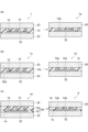
- FIG. 1 is a cross-sectional view showing a wiring formation member according to an embodiment of the present disclosure.
- 2(a) to 2(d) are diagrams for sequentially explaining a method for forming a wiring layer using the wiring forming member shown in FIG. 3A to 3C are cross-sectional views showing wiring-forming members according to another embodiment of the present disclosure and the state in which the wiring-forming members are pressure-bonded together.
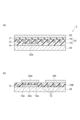
- FIG. 4 is a cross-sectional view showing a wiring formation member according to another embodiment of the present disclosure.
- 5A to 5D are diagrams for sequentially explaining a method for forming a wiring layer using the wiring formation member shown in FIG. 6A and 6B are cross-sectional views for explaining an example in which a wiring layer is formed using the wiring forming member shown in FIG.
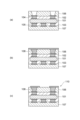
- FIG. 7A and 7B are cross-sectional views for explaining another example in which a wiring layer is formed using the wiring forming member shown in FIG. 8A to 8D are cross-sectional views for sequentially explaining a method for manufacturing a conventional component-embedded substrate.
- 9A to 9C are cross-sectional views for sequentially explaining a method for manufacturing a conventional component-embedded substrate, showing steps subsequent to those in FIG.
- the numerical ranges indicated using “ ⁇ ” include the numerical values before and after " ⁇ " as the minimum and maximum values, respectively.
- the upper or lower limit value described in one numerical range may be replaced with the upper or lower limit value of another numerical range described in stages.
- the upper or lower limit value of that numerical range may be replaced with a value shown in the examples.
- FIG. 1 is a cross-sectional view showing a wiring formation member according to one embodiment of the present disclosure.
- the wiring formation member 1 is configured to include an adhesive layer 10 and a metal layer 20.
- the wiring formation member 1 is a member that can be used, for example, when producing a redistribution layer, a build-up multilayer wiring board, a component-embedded board, and the like, but is not limited thereto.
- the wiring formation member 1 may also be used for EMI shielding, etc.
- the adhesive layer 10 includes conductive particles 12 and an insulating adhesive component 14 in which the conductive particles 12 are dispersed.
- the adhesive component 14 of the adhesive layer 10 is defined as solids other than the conductive particles 12.
- the adhesive layer 10 may be in a B-stage state, i.e., a semi-cured state, before the wiring layer is formed by the wiring forming member 1.
- the conductive particles 12 are substantially spherical particles having electrical conductivity, and are composed of metal particles made of metals such as Au, Ag, Ni, Cu, solder, or conductive carbon particles made of conductive carbon.
- the conductive particles 12 may be coated conductive particles having a core containing non-conductive glass, ceramic, plastic (polystyrene, etc.), and a coating layer containing the above metal or conductive carbon and coating the core.
- the conductive particles 12 may be metal particles formed of a heat-fusible metal, or coated conductive particles having a core containing plastic and a coating layer containing a metal or conductive carbon and coating the core.
- the conductive particles 12 may be copper particles from the viewpoint of making it difficult for a circuit to short circuit.
- the conductive particles 12 include a core made of a polymer particle (plastic particle) such as polystyrene, and a metal layer covering the core.
- the polymer particle may have substantially the entire surface covered with the metal layer, or a part of the surface of the polymer particle may be exposed without being covered with the metal layer, as long as the function as a connecting material is maintained.
- the polymer particle may be, for example, a particle containing a polymer containing at least one monomer selected from styrene and divinylbenzene as a monomer unit.
- the metal layer may be formed of various metals such as Ni, Ni/Au, Ni/Pd, Cu, NiB, Ag, Ru, etc.
- the metal layer may be an alloy layer made of an alloy of Ni and Au, an alloy of Ni and Pd, etc.
- the metal layer may have a multilayer structure made of multiple metal layers.
- the metal layer may be made of a Ni layer and an Au layer.
- the metal layer may be made by plating, vapor deposition, sputtering, soldering, etc.
- the metal layer may be a thin film (for example, a thin film formed by plating, vapor deposition, sputtering, etc.).
- the conductive particle 12 may have an insulating layer.
- an insulating layer may be provided on the outside of the coating layer to further cover the coating layer.
- the insulating layer may be the outermost layer located on the outermost surface of the conductive particle.
- the insulating layer may be a layer formed from an insulating material such as silica or acrylic resin.
- the average particle size Dp of the conductive particles 12 may be 1 ⁇ m or more, 2 ⁇ m or more, or 5 ⁇ m or more, from the viewpoint of excellent dispersibility and conductivity.
- the average particle size Dp of the conductive particles may be 50 ⁇ m or less, 30 ⁇ m or less, or 20 ⁇ m or less, from the viewpoint of excellent dispersibility and conductivity. From the above viewpoint, the average particle size Dp of the conductive particles may be 1 to 50 ⁇ m, 5 to 30 ⁇ m, 5 to 20 ⁇ m, or 2 to 20 ⁇ m.
- the maximum particle size of the conductive particles 12 may be smaller than the minimum spacing between electrodes in the wiring pattern (the shortest distance between adjacent electrodes). From the viewpoint of excellent dispersibility and conductivity, the maximum particle size of the conductive particles 12 may be 1 ⁇ m or more, 2 ⁇ m or more, or 5 ⁇ m or more. From the viewpoint of excellent dispersibility and conductivity, the maximum particle size of the conductive particles may be 50 ⁇ m or less, 30 ⁇ m or less, or 20 ⁇ m or less. From the above viewpoint, the maximum particle size of the conductive particles may be 1 to 50 ⁇ m, 2 to 30 ⁇ m, or 5 to 20 ⁇ m.
- the particle size of any 300 particles is measured by observation using a scanning electron microscope (SEM), the average particle size obtained is defined as the average particle size Dp, and the largest value obtained is defined as the maximum particle size of the particle. Note that if the particle has protrusions or is otherwise not spherical, the particle size is defined as the diameter of the circle circumscribing the particle in the SEM image.
- the content of the conductive particles 12 is determined according to the fineness of the electrodes to be connected.
- the amount of the conductive particles 12 is not particularly limited, but may be 0.1 volume % or more, 0.2 volume % or more, 1 volume % or more, 1.5 volume % or more, 2 volume % or more, 5 volume % or more, or 10 volume % or more based on the total volume of the adhesive components (components in the adhesive composition excluding the conductive particles). When the amount is within these ranges, resistance unevenness and low conductivity tend to be suppressed.
- the amount of the conductive particles 12 may be 30 volume % or less, 15 volume % or less, or 10 volume % or less based on the total volume of the adhesive components (components in the adhesive composition excluding the conductive particles 12). When the amount is within these ranges, short circuits tend to be less likely to occur.
- the "volume %" is determined based on the volume of each component before hardening at 23°C, but the volume of each component can be converted from weight to volume using specific gravity. Alternatively, the component can be poured into a measuring cylinder or other container filled with a suitable solvent (water, alcohol, etc.) that wets the component well without dissolving or swelling it, and the increased volume can be calculated as the volume of the component.
- the adhesive layer 10 may contain 0.1 to 10 volume %, 1 to 5 volume %, or 1 to 3 volume % copper particles as conductive particles.
- the adhesive component 14 constituting the adhesive layer 10 contains a thermosetting component.
- the thermosetting component includes a thermosetting resin, a curing agent, and a curing accelerator.
- Thermosetting resins are resins that are hardened by heat.
- thermosetting resins include epoxy resins, polyimide resins, triazine resins such as melamine resins, phenolic resins, and modified versions of these resins.
- epoxy resins are preferred from the viewpoint of adequately suppressing the occurrence of bubbles or peeling during wiring formation.
- the adhesive component can contain epoxy resin and phenol resin as thermosetting components to sufficiently suppress the occurrence of air bubbles or peeling during wiring formation and to make it difficult for uneven resistance to occur.
- the epoxy resin may be any compound having two or more epoxy groups in the molecule, and examples thereof include bisphenol A type epoxy resin, bisphenol F type epoxy resin, bisphenol S type epoxy resin, biphenyl type epoxy resin, biphenyl novolac type epoxy resin, phenol novolac type epoxy resin, cresol novolac type epoxy resin, bisphenol A novolac type epoxy resin, bisphenol F novolac type epoxy resin, dicyclopentadiene type epoxy resin, alicyclic epoxy resin, aliphatic linear epoxy resin, glycidyl ester type epoxy resin, isocyanurate type epoxy resin, hydantoin type epoxy resin, glycidyl ether compound of polyfunctional phenol, glycidyl ether compound of bifunctional alcohol, and hydrogenated products thereof.
- novolac type epoxy resins such as biphenyl novolac type epoxy resin, phenol novolac type epoxy resin, cresol novolac type epoxy resin, bisphenol A novolac type epoxy resin, or bisphenol F novolac type epoxy resin may be used from the viewpoint of ease of handling and availability.
- the epoxy resin may be used alone or in combination of two or more types.
- the adhesive component may contain, as an epoxy resin, a compound having three or more epoxy groups in one molecule, in order to ensure adhesive strength and heat resistance.
- the epoxy resin may have an epoxy equivalent of 100 to 1000 g/eq, 125 to 900 g/eq, or 150 to 800 g/eq.
- the epoxy equivalent is determined by a method standardized in the JIS standard (K7236:2001).
- the content of the epoxy resin in the adhesive component may be 5-95% by mass, 10-90% by mass, 15-85% by mass, or 40-60% by mass, based on the total amount of the adhesive component (total amount of solids other than the conductive particles 12 in the adhesive layer 10).
- Phenolic resins function as hardeners for epoxy resins.
- phenolic resins include novolac-type phenolic resins such as phenol novolac, cresol novolac, bisphenol A novolac, bisphenol F novolac, and catechol novolac, as well as those in which the aromatic rings are substituted with alkyl groups.
- One type of phenolic resin may be used alone, or two or more types may be used in combination.
- the adhesive component may contain, as a phenolic resin, a compound having three or more phenol groups or cresol groups in one molecule, from the viewpoint of ensuring adhesive strength and heat resistance.
- a phenolic resin a compound having three or more phenol groups or cresol groups in one molecule
- phenol novolac type phenolic resin cresol novolac type phenolic resin
- bisphenol A novolac type phenolic resin bisphenol F novolac type phenolic resin, etc.
- the hydroxyl group equivalent of the phenolic resin may be 300 g/eq or less, or 250 g/eq or less, from the viewpoint of suppressing the occurrence of bubbles or peeling during wiring formation and making it difficult for uneven resistance to occur, and may be 50 g/eq or more, or 100 g/eq or more, from the viewpoint of ease of handling and good reactivity.
- the hydroxyl equivalent of the phenol resin can be determined by the following measurement method. ⁇ Method for measuring hydroxyl equivalent> 1 g of sample is precisely weighed into a round-bottom flask, and 5 mL of acetic anhydride and pyridine test solution are precisely weighed. Next, an air condenser is attached to the flask, and the flask is heated at 100°C for 1 hour. After cooling the flask, 1 mL of water is added, and the flask is heated again at 100°C for 10 minutes. After cooling the flask again, the air condenser and the neck of the flask are washed with 5 mL of neutralized methanol, and 1 mL of phenolphthalein reagent is added.
- the solution thus obtained is titrated with a 0.1 mol/L potassium hydroxide-ethanol solution to determine the hydroxyl value. From the obtained hydroxyl value, the hydroxyl equivalent (g/eq) converted to the mass per 1 mol (1 eq) of hydroxyl is calculated.
- the amount of phenolic resin in the adhesive component can be set so that the number of hydroxyl groups in the phenolic resin is 0.5 to 2 per epoxy group in the epoxy resin.
- the adhesive component containing epoxy resin and phenolic resin may further contain a thermosetting resin other than epoxy resin, and may further contain a curing agent other than phenolic resin.
- a thermosetting resin other than epoxy resin polyimide resin, triazine resin such as melamine resin, and modified products of these resins can be used.
- a curing agent other than phenolic resin amines, amides, acid anhydrides, acids, imidazoles, etc. can be used.
- the adhesive component can further contain a maleimide compound from the viewpoint of sufficiently suppressing the occurrence of air bubbles or peeling during wiring formation.
- the adhesive component may contain an epoxy resin as a thermosetting resin.
- the content of the epoxy resin in the adhesive component may be 5 to 95 mass %, 10 to 90 mass %, 15 to 85 mass %, or 15 to 40 mass %, based on the total amount of the adhesive component (total amount of solids other than the conductive particles 12 in the adhesive layer 10).
- the maleimide compound is a compound having at least one N-substituted maleimide group in one molecular structure.
- the maleimide compound may contain at least one selected from the group consisting of a polymaleimide compound (m1) (hereinafter sometimes referred to as "(m1) component") having at least two N-substituted maleimide groups in one molecular structure and its derivatives.
- m1 polymaleimide compound
- derivatives include an addition reaction product between the polymaleimide compound (m1) and an amine compound such as a diamine compound described below. Since maleimide compounds have low reactivity, it is expected that the curing reaction will proceed slowly by including them in the adhesive component 14. The slow progress of the curing reaction ensures sufficient flow time, making it possible to sufficiently suppress the occurrence of bubbles or peeling during wiring formation.
- Examples of the (m1) component include N,N'-ethylene bismaleimide, N,N'-hexamethylene bismaleimide, N,N'-(1,3-phenylene) bismaleimide, N,N'-[1,3-(2-methylphenylene)] bismaleimide, N,N'-[1,3-(4-methylphenylene)] bismaleimide, N,N'-(1,4-phenylene) bismaleimide, bis(4-maleimidophenyl)methane, bis(3-methyl-4-maleimidophenyl)methane, 3,3-di Methyl-5,5-diethyl-4,4-diphenylmethane bismaleimide, bis(4-maleimidophenyl)ether, bis(4-maleimidophenyl)sulfone, bis(4-maleimidophenyl)sulfide, bis(4-maleimidophenyl)ketone, bis(4-maleimidocyclo
- maleimide compounds bis(4-maleimidophenyl)methane, bis(4-maleimidophenyl)sulfone, N,N'-(1,3-phenylene)bismaleimide, 2,2-bis(4-(4-maleimidophenoxy)phenyl)propane, or polyphenylmethanemaleimide are preferred, as they have a high reaction rate and can be made more heat resistant, and bis(4-maleimidophenyl)methane is particularly preferred in terms of solubility in solvents.
- the maleimide compound may contain a derivative of a polymaleimide compound (m1) from the viewpoints of solubility in organic solvents, compatibility, and adhesion to metal foils.
- the derivative of the polymaleimide compound (m1) may contain, for example, a modified polymaleimide compound (M) having a structural unit derived from the polymaleimide compound (m1) and a structural unit derived from an amine compound (m2) having an amino group (hereinafter sometimes referred to as "component (m2)").
- component (m2) a modified polymaleimide compound having a structural unit derived from the polymaleimide compound (m2) having an amino group
- component (m2) hereinafter sometimes referred to as "component (m2)"
- the modified polymaleimide compound (M) can also be said to be an addition reaction product of the component (m1) and the component (m2).
- the modified polymaleimide compound (M) may be a compound containing a structure represented by the following formula (1), which is formed by an addition reaction between a maleimide group in the (m1) component and an amino group in the (m2) component.
- formula (1) * indicates the bond position.
- the (m2) component is preferably an amine compound (polyamine compound) having at least two amino groups, and may be a diamine compound having two amino groups.
- Examples of the (m2) component include 4,4'-diaminodiphenylmethane, 4,4'-diamino-3,3'-dimethyldiphenylmethane, 3,3'-diethyl-4,4'-diaminodiphenylmethane, 4,4'-diaminodiphenyl ether, 4,4'-diaminodiphenyl sulfone, 3,3'-diaminodiphenyl sulfone, 4,4'-diaminodiphenyl ketone, 4,4'-diaminobiphenyl, 3,3'-dimethyl-4,4'- Diaminobiphenyl, 2,2'-dimethyl-4,4'-diaminobiphenyl, 3,3'-dihydroxybenzidine, 2,2-bis(
- the (m2) component may be an amine compound having a siloxane skeleton from the viewpoint of low thermal expansion.
- the modified polymaleimide compound (M) may have a structural unit derived from the polymaleimide compound (m1) and a structural unit derived from an amine compound having a siloxane skeleton.
- the (m2) component may be a compound represented by the following general formula (2):
- X b4 represents a divalent organic group.
- the component (m2) may contain an amine compound having a siloxane skeleton in which X b4 in the above general formula (2) has a structural unit represented by the following general formula (3): Furthermore, the component (m2) may contain an amine compound having a siloxane skeleton in which X b4 has a structural unit (or group) represented by the following general formula (4):
- R b16 and R b17 each independently represent an alkyl group having 1 to 5 carbon atoms, a phenyl group, or a substituted phenyl group. * indicates the bonding position.
- R b16 and R b17 have the same meaning as R b16 and R b17 in general formula (3), and a plurality of R b16 and R b17 may be the same or different.
- R b18 and R b19 each independently represent an alkyl group having 1 to 5 carbon atoms, a phenyl group, or a substituted phenyl group.
- X b9 and X b10 each independently represent a divalent organic group, and n b13 represents an integer of 2 to 100.
- Examples of the substituent in the substituted phenyl group represented by R b16 , R b17 , R b18 , and R b19 include an alkyl group having 1 to 5 carbon atoms, an alkenyl group having 2 to 5 carbon atoms, and an alkynyl group having 2 to 5 carbon atoms.
- Examples of the divalent organic group represented by X b9 and X b10 include an alkylene group, an alkenylene group, an alkynylene group, an arylene group, --O--, or a divalent linking group formed by combining these groups.
- the content of structural units derived from component (m1) in the modified polymaleimide compound (M) is not particularly limited, but may be 50 to 95% by mass, 70 to 92% by mass, or 75 to 90% by mass.
- the content of structural units derived from component (m2) in modified polymaleimide compound (M) is not particularly limited, but may be 5 to 50% by mass, 8 to 30% by mass, or 10 to 25% by mass.
- the total content of the structural units derived from the (m1) component and the structural units derived from the (m2) component in the modified polymaleimide compound (M) is not particularly limited, but may be 80% by mass or more, 90% by mass or more, 95% by mass or more, or 100% by mass (i.e., consisting only of the structural units derived from the (m1) component and the structural units derived from the (m2) component).
- the content of the maleimide compound in the adhesive component may be 5 to 95 mass %, 10 to 90 mass %, or 15 to 85 mass %, based on the total amount of the adhesive component (total amount of solids other than the conductive particles 12 in the adhesive layer 10).
- the curing accelerator examples include imidazole compounds, organic phosphorus compounds, tertiary amines, and quaternary ammonium salts.
- One type of curing accelerator may be used alone, or two or more types may be used in combination.
- the adhesive component may contain an imidazole compound as a curing accelerator, from the viewpoint of being able to freely adjust the temperature and time during use (for example, the heating temperature and heating time during heat-pressure bonding).
- the content of the curing accelerator in the adhesive component may be 0.001 to 10 mass % based on the total amount of the adhesive component.
- the adhesive component 14 may contain other components in addition to the thermosetting components described above.
- the other components may further include a filler, an antioxidant, a film-forming material, a softener, an anti-aging agent, a colorant, a flame retardant, a thixotropic agent, a coupling agent, etc.
- Fillers include inorganic fillers and organic fillers.
- Inorganic fillers include alumina, silica, titanium oxide, clay, calcium carbonate, aluminum carbonate, magnesium silicate, aluminum silicate, mica, short glass fibers, aluminum borate, silicon carbide, etc.
- Organic fillers include silicone particles, methacrylate-butadiene-styrene particles, acrylic-silicone particles, polyamide particles, polyimide particles, etc. Fillers may be used alone or in combination of two or more types.
- the adhesive component may contain silica particles as a filler to improve heat resistance, improve mechanical properties, and adjust flowability during use (e.g., during heat bonding).
- the maximum diameter of the filler may be less than the particle size of the conductive particles 12, and may be 0.001 to 10 ⁇ m.
- the filler content may be 5 to 60 parts by volume per 100 parts by volume of the adhesive component. When the filler content is 5 to 60 parts by volume, good connection reliability tends to be obtained.
- antioxidants examples include quinone derivatives such as benzoquinone and hydroquinone, phenol derivatives (hindered phenol derivatives) such as 4-methoxyphenol and 4-t-butylcatechol, aminoxyl derivatives such as 2,2,6,6-tetramethylpiperidine-1-oxyl and 4-hydroxy-2,2,6,6-tetramethylpiperidine-1-oxyl, and hindered amine derivatives such as tetramethylpiperidyl methacrylate.
- quinone derivatives such as benzoquinone and hydroquinone
- phenol derivatives hindered amine derivatives
- hindered amine derivatives such as tetramethylpiperidyl methacrylate.
- the content of the antioxidant may be 0.01% by mass to 5% by mass, or 0.1% by mass to 3% by mass, based on the total amount of the adhesive components.
- thermoplastic resin is preferably used, and examples thereof include phenoxy resin, polyvinyl formal resin, polystyrene resin, polyvinyl butyral resin, polyester resin, polyamide resin, xylene resin, polyurethane resin, polyacrylic resin, polyester urethane resin, and the like. Furthermore, these polymers may contain siloxane bonds or fluorine substituents. These resins may be used alone or in a mixture of two or more types. Among the above resins, phenoxy resin may be used from the viewpoints of adhesive strength, compatibility, heat resistance, and mechanical strength.
- the molecular weight of the thermoplastic resin may be 5,000 to 150,000, or 10,000 to 80,000, in terms of weight average molecular weight. By making the weight average molecular weight 5,000 or more, good film formability is easily obtained, and by making it 150,000 or less, good compatibility with other components is easily obtained.
- the weight average molecular weight refers to a value measured by gel permeation chromatography (GPC) using a calibration curve based on standard polystyrene under the following conditions.
- GPC gel permeation chromatography
- the content of the film-forming material may be 0.5 to 75% by mass, or 1 to 50% by mass, based on the total amount of the adhesive components.
- the adhesive component 14 may be substantially free of highly reactive radically polymerizable compounds such as acrylic compounds, methacrylic compounds, styrene compounds, and vinyl compounds. Note that “substantially free” means that the content is 1% by mass or less based on the total amount of the adhesive component.
- the content of the above compounds in the adhesive component may be 0.5% by mass or less, or may be 0% by mass, based on the total amount of the adhesive component.
- the adhesive layer 10 may have a reaction rate of 90% or less, 85% or less, 80% or less, or 70% or less when heated at 180°C for 5 minutes.
- the above reaction rate refers to a value determined by the following measurement method. [Measurement of reaction rate when heated at 180° C. for 5 minutes] A part of the adhesive layer is scraped off to obtain two 5 mg samples for evaluation before heating. Next, one of the samples for evaluation before heating is heated at 180°C for 5 minutes to obtain a sample for evaluation after heating. For each of the samples for evaluation before heating and the samples for evaluation after heating, a differential scanning calorimetry (DSC) device (product name DSC7, manufactured by PERKIN ELMER) is used to measure the DSC calorific value under a nitrogen gas flow at a measurement temperature range of 30°C to 250°C and a heating rate of 2°C/min.
- DSC differential scanning calorimetry
- reaction rate (Cx - Cy) x 100/Cx
- Cx represents the DSC calorific value (J/g) of the evaluation sample before heating
- Cy represents the DSC calorific value (J/g) of the evaluation sample after heating.
- the reaction rate of the adhesive layer when heated at 180°C for 5 minutes can be reduced by, for example, adding the above-mentioned phenolic resin or maleimide compound, not adding a curing accelerator, or selecting a curing accelerator with a high reaction initiation temperature.
- the ratio [Dp/T] of the average particle diameter Dp of the conductive particles to the thickness T of the adhesive layer may be 0.56 to 1.2, 0.6 to 1.15, or 0.65 to 1.1.
- the thickness of the adhesive layer may be 1 to 70 ⁇ m, 2 to 60 ⁇ m, or 3 to 50 ⁇ m.
- the surface roughness Rz of one surface of the metal layer 20 and the surface opposite thereto may be equal or different.
- the metal layer 20 has a thickness of, for example, 5 ⁇ m to 200 ⁇ m.
- the thickness of the metal layer here is a thickness including the surface roughness Rz.
- the metal layer 20 is, for example, copper foil, aluminum foil, nickel foil, stainless steel, titanium, or platinum.
- the adhesive layer 10 is disposed on the first surface 20a of the metal layer 20.
- the surface roughness Rz of the first surface 20a of the metal layer 20 may be 0.3 ⁇ m or more, 0.5 ⁇ m or more, or 1.0 ⁇ m or more.
- the surface roughness Rz of the first surface 20a of the metal layer 20 may be 50 ⁇ m or less, 40 ⁇ m or less, 30 ⁇ m or less, 20 ⁇ m or less, less than 20 ⁇ m, 17 ⁇ m or less, 10 ⁇ m or less, 8.0 ⁇ m or less, 5.0 ⁇ m or less, or 3.0 ⁇ m or less.
- the surface roughness Rz of the first surface 20a of the metal layer 20 may be, for example, 0.3 ⁇ m or more and 20 ⁇ m or less, 0.3 ⁇ m or more and less than 20 ⁇ m, or more specifically, 0.5 ⁇ m or more and 10 ⁇ m or less.
- the surface roughness Rz of the second surface 20b of the metal layer 20 may be, for example, 20 ⁇ m or more, may be rougher than the surface roughness Rz of the first surface 20a, may be the same surface roughness as the first surface 20a, or may not be rougher than the surface roughness Rz of the first surface 20a.
- the surface roughness Rz of the first surface 20a of the metal layer 20 is too smooth (for example, the surface roughness Rz is 0.2 ⁇ m), the adhesion between the metal layer 20 and the adhesive layer 10 may not be maintained for a long period of time and may peel off. For this reason, the surface roughness Rz of the first surface 20a of the metal layer 20 may be 0.3 ⁇ m or more. However, the surface roughness Rz of the first surface 20a of the metal layer 20 may be less than 0.3 ⁇ m by adopting a material or connection configuration that can ensure adhesion.
- Surface roughness Rz refers to the ten-point average roughness Rzjis measured in accordance with the method specified in the JIS standard (JIS B 0601-2001), and refers to the value measured using a commercially available surface roughness profile measuring instrument. For example, it can be measured using a nano search microscope (Shimadzu Corporation's "SFT-3500").
- the "surface roughness/average particle diameter" which is the ratio of the surface roughness Rz of the first surface 20a of the metal layer 20 to the average particle diameter Dp of the conductive particles 12 may be 0.03 or more, 0.04 or more, 0.05 or more, 0.06 or more, 0.1 or more, 0.2 or more, 0.3 or more, 0.5 or more, or 1 or more.
- the "surface roughness/average particle diameter" which is the ratio of the surface roughness Rz of the first surface 20a of the metal layer 20 to the average particle diameter Dp of the conductive particles 12 may be 3 or less, 2 or less, 1.7 or less, or 1.5 or less.
- the ratio of the surface roughness Rz of the first surface 20a of the metal layer 20 to the average particle diameter Dp of the conductive particles 12, "surface roughness/average particle diameter" may be, for example, 0.05 or more and 3 or less, and more specifically, 0.06 or more and 2 or less.
- the surface roughness Rz of the first surface 20a of the metal layer 20 and the average particle diameter Dp of the conductive particles 12 may be controlled so that the ratio of the surface roughness Rz of the first surface 20a of the metal layer 20 to the average particle diameter Dp of the conductive particles 12, "surface roughness/average particle diameter", is in the range of 0.05 to 3.
- the present disclosure relates to a method for forming a wiring layer using a wiring formation member.
- the method for forming a wiring layer using the wiring formation member 1 described above will be described with reference to FIG. 2.
- (a) to (d) of FIG. 2 are diagrams showing a method for forming a wiring layer using the wiring formation member shown in FIG. 1.
- a wiring forming member 1 as shown in FIG. 2(a). Then prepare a base material 30 on which wiring 32 is formed. Then, arrange the wiring forming member 1 so that the adhesive layer 10 side of the wiring forming member 1 faces the base material 30. After that, as shown in FIG. 2(b), laminate is performed so as to cover the wiring 32, and the wiring forming member 1 is attached onto the base material 30.
- a predetermined patterning process e.g., etching process
- the metal layer 20 may process it into a predetermined wiring pattern 20c (another wiring).
- the second surface 20b of the metal layer 20 may be processed to make it a smooth surface.
- the above-mentioned processes in FIG. 2(a) to (d) may be repeated a predetermined number of times to form a wiring layer.
- the method for forming a wiring layer using a wiring forming member includes the steps of preparing a wiring forming member, preparing a base material on which wiring is formed, placing the wiring forming member on the surface of the base material on which wiring is formed so that the adhesive layer side faces the substrate and covers the wiring, heating and pressing the wiring forming member to the base material, and performing a patterning process on the metal layer.
- the above steps form the wiring member 1b.
- the wiring member 1b includes a substrate 30 having wiring 32, and a cured product of the adhesive component 14 of the wiring member 1 (adhesive layer of the wiring member bonded by heating and pressing) that is placed on the substrate 30 so as to cover the wiring 32.
- the wiring 32 and the metal layer 20 of the wiring member 1 or the wiring 20c formed (e.g., by etching) from the metal layer 20 are electrically connected by the conductive particles 12a.
- the wiring member 1b may have a configuration having multiple wiring layers (layers that connect the above-mentioned wirings to each other).
- the method for forming a wiring layer using the wiring formation member 1 according to this embodiment can simplify the process for forming the wiring layer that connects the wirings, compared to conventional processes that involve laser processing and field plating.
- the formed wiring layer can be easily thinned.
- the adhesive layer 10 has the above-mentioned reaction rate and the ratio [Dp/T] of the average particle diameter Dp of the conductive particles 12 to the thickness T of the adhesive layer 10 is 0.56 to 1.2, a wiring layer with suppressed resistance unevenness can be formed.
- the present disclosure is not limited to the above embodiments and can be applied to various embodiments.
- the conductive particles 12 are randomly or evenly dispersed in the adhesive layer 10 in the wiring forming member 1, but as shown in (b) of FIG. 3, the conductive particles 12 may be arranged (distributed) on the metal layer 20 side.
- the conductive particles 12 are not exposed on the second surface 10b opposite to the metal layer 20, and the thickness of the adhesive layer 10 existing between the conductive particles 12 and the first surface 20a of the metal layer 20 may be greater than 0 ⁇ m or 0.1 ⁇ m and less than 1 ⁇ m.
- the conductive particles 12 are arranged on the metal layer 20 side, it is possible to more reliably crush the conductive particles 12 into a flat shape by the metal layer 20 in the wiring layer 1d.
- the capture rate of the conductive particles 12 to the wiring (electrode) or the like can be improved. That is, the conduction can be made more stable.
- the distance between the conductive particles 12 and the first surface 20a of the metal layer 20 (the thickness of the adhesive layer 10 between them) means the shortest distance from the surface of the metal layer 20 in contact with the adhesive layer 10 to the surface of the conductive particles 12, and is, for example, the average value at any 30 points.
- This distance is measured by sandwiching the wiring forming member between two pieces of glass (thickness: about 1 mm), casting it with a resin composition consisting of 100 g of bisphenol A type epoxy resin (product name: JER811, manufactured by Mitsubishi Chemical Corporation) and 10 g of a hardener (product name: Epomount Hardener, manufactured by Refine Tech Co., Ltd.), polishing the cross section with a polishing machine, and measuring it with a scanning electron microscope (SEM, product name: SE-8020, manufactured by Hitachi High-Tech Science Corporation).
- a resin composition consisting of 100 g of bisphenol A type epoxy resin (product name: JER811, manufactured by Mitsubishi Chemical Corporation) and 10 g of a hardener (product name: Epomount Hardener, manufactured by Refine Tech Co., Ltd.), polishing the cross section with a polishing machine, and measuring it with a scanning electron microscope (SEM, product name: SE-8020, manufactured by Hitachi High-Tech Science Corporation).
- the adhesive layer 10d may be divided into a first adhesive layer 10e and a second adhesive layer 10f.
- the adhesive components constituting the first adhesive layer 10e and the second adhesive layer 10f may be the same as the adhesive components constituting the adhesive layer 10 described above, but the difference is that the conductive particles 12 are not dispersed, i.e., are not included, in the second adhesive layer 10f.
- the adhesive layer 10d has the above-mentioned reaction rate and the ratio [Dp/T] of the average particle diameter Dp of the conductive particles 12 to the thickness T of the adhesive layer 10 is 0.56 to 1.2, a wiring layer with suppressed resistance unevenness can be formed.
- the conductive particles 12 are dispersed, i.e., included, in the first adhesive layer 10e.
- the conductive particles 12 are arranged on the metal layer 20 side, so that the conductive particles 12 can be more reliably crushed into a flat shape by the metal layer 20 in the wiring layer 1f.
- the capture rate of the conductive particles 12 in the wiring (electrodes) etc. can be improved. In other words, the conduction can be made more stable.
- the wiring forming member 1, 1c, 1e may further include a release film.
- the release film may be attached to the side of the adhesive layer 10, 10c, 10d opposite to the side to which the metal layer 20 is attached, or may be attached to the side of the metal layer 20 opposite to the side to which the adhesive layer 10, 10c, 10d is attached, or may be attached to both of these.
- the first surface 20a of the metal layer 20 may be attached to the adhesive layer 10, 10c, 10d. In this case, the wiring forming member becomes easier to handle, and the work efficiency can be improved when forming a wiring layer using the wiring forming member.
- the wiring-forming member is a member formed by bonding the adhesive layer 10 and the metal layer 20
- the wiring-forming member in this embodiment may be configured as a set in which the adhesive layer 10 and the metal layer 20 are provided separately and the adhesive layer 10 can be bonded to the first surface 20a of the metal layer 20 during use.
- the adhesive layer 10 and the metal layer 20 can be prepared separately (as a set of wiring-forming members), it is possible to improve the degree of freedom in the work when fabricating a wiring layer using the wiring-forming member, such as by selecting a wiring-forming member with a more optimal material composition.
- FIG. 4 is a cross-sectional view showing a wiring forming member according to another embodiment of the present disclosure.
- the wiring forming member 2 shown in FIG. 4 is configured to include an adhesive layer 10 containing conductive particles 12, and a metal layer 20.
- the adhesive layer 10 includes a first adhesive layer 15 containing conductive particles 12 and an adhesive component 14, and a second adhesive layer 16 containing an adhesive component 17.
- the first adhesive layer 15 contains conductive particles 12 and an insulating adhesive component 14 in which the conductive particles 12 are dispersed.
- the adhesive component 14 is the same as that described above.
- the second adhesive layer 16 includes an insulating adhesive component 17.
- the insulating adhesive component 17 in the second adhesive layer 16 may be the same as or different from the adhesive component 14.
- the adhesive component 17 in the second adhesive layer 16 is defined as a solid content other than conductive particles.
- the second adhesive layer 16 may be in a B-stage state, i.e., a semi-cured state, before the wiring layer is formed by the wiring forming member 2.
- the reactivity of the first adhesive layer 15 and the second adhesive layer 16 is adjusted so that the adhesive layer 10 has the above-mentioned reaction rate, and the average particle size of the conductive particles 12 and the thicknesses of the first adhesive layer 15 and the second adhesive layer 16 may be adjusted so that the ratio [Dp/T] of the average particle size Dp of the conductive particles 12 to the thickness T of the adhesive layer 10 is within the above-mentioned range.
- the thickness d1 of the first adhesive layer 15 may be 0.56 to 1.2 times, 0.56 to 1.0 times, or 0.56 to 0.80 times the average particle size Dp of the conductive particles 12.
- the thickness of the first adhesive layer 15 may be 1 to 70 ⁇ m, 1 to 60 ⁇ m, or 1 to 50 ⁇ m.
- the thickness of the second adhesive layer 16 may be 0 to 50 ⁇ m, 0 to 40 ⁇ m, or 0 to 30 ⁇ m.
- FIG. 5 are diagrams showing a method for forming a wiring layer using the wiring forming member shown in FIG. 4.
- a wiring forming member 2 is prepared. Furthermore, a base material 30 on which wiring 32 is formed is prepared. Then, the wiring forming member 2 is arranged so that the adhesive layer 10 side of the wiring forming member 2 faces the base material 30. After that, as shown in FIG. 5(b), lamination is performed so as to cover the wiring 32, and the wiring forming member 2 is attached onto the base material 30.
- the wiring forming member 2 is heated and pressurized to a predetermined degree, and is pressed against the substrate 30.
- the conductive particles 12 that need to ensure conductivity can be more reliably deformed into flat conductive particles 12a.
- the flattened conductive particles 12a (whereby the insulating layer is destroyed and the conductive portion is exposed) are arranged on the wiring 32, and good electrical conduction between the metal layer 20 and the wiring 32 is achieved.
- the adhesive layer 10 is also crushed to become a thinner adhesive layer 10B.
- the adhesive layer 10 includes the first adhesive layer 15 in which conductive particles are contained in the adhesive component, and the second adhesive layer 16, good insulation reliability is achieved in the thickness direction of the portion where electrical connection is not desired.
- a predetermined patterning process e.g., etching process
- the metal layer 20 may process it into a predetermined wiring pattern 20c (another wiring).
- the second surface 20b of the metal layer 20 may be processed to make it a smooth surface.
- the above-mentioned processes in FIG. 5(a) to (d) may be repeated a predetermined number of times to form a wiring layer.
- the method for forming a wiring layer using a wiring forming member includes the steps of preparing a wiring forming member, preparing a base material on which wiring is formed, placing the wiring forming member on the surface of the base material on which wiring is formed so that the adhesive layer side faces the substrate and covers the wiring, heating and pressing the wiring forming member to the base material, and performing a patterning process on the metal layer.
- the above steps form the wiring member 2b.
- the wiring member 2b includes a base material 30 having wiring 32, and a cured product (adhesive layer of the wiring member bonded by heating and pressing) of the first adhesive layer 15 and the second adhesive layer 16 of the wiring member 2 arranged on the base material 30 so as to cover the wiring 32.
- the wiring 32 and the metal layer 20 of the wiring member 2 or the wiring pattern 20c formed (e.g., by etching) from the metal layer 20 are electrically connected by the conductive particles 12a.
- the wiring member 2b may have a configuration having multiple wiring layers (layers connecting the above-mentioned wirings).
- the method of forming a wiring layer using the wiring formation member 2 according to this embodiment can simplify the process of forming the wiring layer that connects the wirings, compared to conventional processes that involve laser processing and field plating.
- the formed wiring layer can be easily thinned.
- the adhesive layer 10 has the above-mentioned reaction rate and the ratio [Dp/T] of the average particle diameter Dp of the conductive particles 12 to the thickness T of the adhesive layer 10 is 0.56 to 1.2, a wiring layer with suppressed resistance unevenness can be formed.
- the following effects can ensure sufficient freedom in designing the wiring pattern when forming the wiring layer.
- the adhesive layer 10 includes the second adhesive layer 16
- the conductive particles 12 are less likely to come into contact with parts other than the parts that are electrically connected, making it easier to suppress electrical transmission loss in the wiring due to contact of the conductive particles.
- FIG. 6 are cross-sectional views illustrating an example of a case where a wiring layer is formed using the wiring formation member 2 according to this embodiment.
- FIG. 6 shows a state in which a substrate 30 having wiring patterns 32a and 32b is prepared, and a wiring forming member 2 is placed on the surface of the substrate 30 on which the wiring patterns are formed so that the adhesive layer 10 side faces the substrate 30 to cover the wiring patterns 32a and 32b.
- a process of heat-pressing the wiring forming member 2 to the substrate 30 and a process of performing a patterning process on the metal layer 20 are performed, thereby obtaining a wiring forming member as shown in (b) in FIG. 6, in which a wiring pattern 20d that is conductively connected to the wiring pattern 32a and a wiring pattern 20e that is not intended to be conductively connected to the wiring pattern 32b are formed.
- the adhesive layer 10 of the wiring forming member 2 includes a first adhesive layer 15 containing conductive particles 12 and adhesive component 14, and a second adhesive layer 16 containing no conductive particles and containing adhesive component 17. This ensures good electrical continuity between the wiring patterns 20d and 32a via the conductive particles 12 when pressed together, while providing an adhesive layer 18a with a thickness that ensures a distance between the wiring patterns 20e and 32b that are not to be electrically connected, so that electrical continuity due to the conductive particles 12 is not generated. This ensures that the wiring patterns 20e and 32b are not electrically connected, and ensures insulation reliability in the thickness direction of the adhesive layer.
- FIG. 7 are cross-sectional views illustrating another example of forming a wiring layer using the wiring formation member 2 according to this embodiment.
- FIG. 7 shows a state in which a substrate 30 having a wiring pattern 32a is prepared, and a wiring forming member 2 is placed on the surface of the substrate 30 on which the wiring pattern is formed so that the adhesive layer 10 side faces the substrate 30 to cover the wiring pattern 32a.
- a process of heat-pressing the wiring forming member 2 to the substrate 30 and a process of performing a patterning process on the metal layer 20 are performed, and a wiring forming member is obtained in which a wiring pattern 20d that is conductively connected to the wiring pattern 32a and a wiring pattern 20f that is not conductively connected (or a portion of the wiring pattern that is not conductively connected) are formed, as shown in (b) in FIG. 7.
- the adhesive layer 10 of the wiring forming member 2 includes a first adhesive layer 15 containing conductive particles 12 and adhesive component 14, and a second adhesive layer 16 containing no conductive particles and containing adhesive component 17.
- the metal layer 20, the second adhesive layer 16, and the first adhesive layer 15 are laminated in this order, making it easy to prevent contact between the wiring pattern 20f and the conductive particles 12.
- the wiring pattern 20f may be formed by a process of performing a patterning process on the metal layer 20 and a process of forming rewiring.
- the conductive particles 12 are arranged locally, but the conductive particles 12 may be dispersed randomly or evenly within the adhesive component 14.
- the conductive particles 12 may be locally arranged on the second adhesive layer 16 side, or the conductive particles 12 may be locally arranged on the opposite side to the second adhesive layer 16 side (the second surface 10b side of the adhesive layer 10).
- the second adhesive layer 16 of the wiring forming member 2 does not contain conductive particles, but the second adhesive layer 16 may contain a portion of the particle body of the conductive particle 12 (in other words, it may not contain the entire particle body of the conductive particle 12).
- the adhesive layer 10 of the wiring forming member 2 may be composed of two layers, the first adhesive layer 15 and the second adhesive layer 16, or may be composed of three or more layers including a layer other than the first adhesive layer 15 and the second adhesive layer 16 (e.g., a third adhesive layer).
- the third adhesive layer may be a layer having a composition similar to the composition described above for the first adhesive layer 15 or the second adhesive layer 16, and may be a layer having a thickness similar to the thickness described above for the first adhesive layer 15 or the second adhesive layer 16.
- the wiring forming member 2 may be composed of a metal layer, a third adhesive layer, a second adhesive layer, and a first adhesive layer laminated in this order, or may be composed of a metal layer, a second adhesive layer, a first adhesive layer, and a third adhesive layer laminated in this order, but is not limited thereto.
- the wiring forming member 2 may further include a release film.
- the release film may be attached to the side of the adhesive layer 10 opposite to the side to which the metal layer 20 is attached (the second surface 10b side of the adhesive layer 10), or may be attached to the side of the metal layer 20 opposite to the side to which the adhesive layer 10 is attached (the first surface 20a of the metal layer) (the second surface 20b side of the metal layer 20), or may be attached to both of these.
- the wiring forming member becomes easier to handle, and the work efficiency can be improved when forming a wiring layer using the wiring forming member.
- the wiring-forming member 2 in this embodiment may be configured as a set in which the adhesive layer 10 and the metal layer 20 are provided separately and the adhesive layer 10 can be bonded to the first surface 20a of the metal layer 20 during use.
- the adhesive layer 10 and the metal layer 20 can be prepared separately (as a set of wiring-forming members), it is possible to improve the degree of freedom in the work when fabricating a wiring layer using the wiring-forming member, such as by selecting a wiring-forming member with a more optimal material composition.
- Synthesis Example 1 Synthesis of modified polymaleimide compound A 2 L reaction vessel equipped with a thermometer, a stirrer, and a moisture content meter with a reflux condenser and capable of being heated and cooled was charged with 100 g of a siloxane modified at both ends with diamines (manufactured by Shin-Etsu Chemical Co., Ltd., product name: X-22-161A, amino functional group equivalent: 800 g/mol), 450 g of 2,2-bis[4-(4-maleimidophenoxy)phenyl]propane, and 550 g of propylene glycol monomethyl ether, and reacted at 120° C. for 3 hours to obtain a solution containing a modified polymaleimide compound.
- the weight average molecular weight (Mw) of the obtained modified maleimide resin was 2500.
- thermosetting component epoxy resin A: NC-3000H (biphenyl novolac type epoxy resin, product name, manufactured by Nippon Kayaku Co., Ltd., epoxy equivalent: 289 g/eq)
- Epoxy resin B NC-7000L (naphthol aralkyl cresol copolymer epoxy resin, product name, manufactured by Nippon Kayaku Co., Ltd., epoxy equivalent: 230 g/eq)
- Phenolic resin A KA-1165 (cresol novolac type phenolic resin, product name, manufactured by DIC Corporation, hydroxyl equivalent: 119 g/eq)
- the hydroxyl equivalent of the phenolic resin was determined by the following measurement method.
- Maleimide compound A modified polymaleimide compound of Synthesis Example 1
- Curing accelerator A G-8009L (isocyanate masked imidazole, product name, manufactured by Daiichi Kogyo Seiyaku Co., Ltd.)
- Silica particles A SC-2050 (KC) (fused spherical silica, average particle size 0.5 ⁇ m, manufactured by Admatechs Co., Ltd., trade name)
- Antioxidant Antioxidant
- Antioxidant A Yoshinox BB (phenol derivative, product name, manufactured by Mitsubishi Chemical Corporation)
- the solution thus obtained was titrated with a 0.1 mol/L potassium hydroxide-ethanol solution to determine the hydroxyl value. From the obtained hydroxyl value, the hydroxyl equivalent (g/eq) converted to the mass per 1 mol (1 eq) of hydroxyl groups was calculated.
- conductive particles As the conductive particles 1, gold-plated resin particles (resin material: styrene-divinylbenzene copolymer), conductive particles having an average particle size of 20 ⁇ m and a specific gravity of 1.7 were prepared.
- Conductive Particles 2 As the conductive particles 2, Ni particles having an average particle size of 20 ⁇ m and a specific gravity of 8.9 were prepared.
- Conductive Particles 3 As the conductive particles 3, Cu particles having an average particle size of 20 ⁇ m and a specific gravity of 8.9 were prepared.
- Example 1 23.12 g of epoxy resin A, 9.52 g of phenolic resin A, and 0.065 g of curing accelerator A were dissolved in 13.05 g of methyl ethyl ketone (MEK), and then 12.56 g of silica particles A and 8.23 g of conductive particles 1 were added to prepare a coating liquid for forming an adhesive layer.
- MEK methyl ethyl ketone
- This coating solution was applied to one side (surface roughness Rz: 3.0 ⁇ m) of copper foil (manufactured by Mitsui Mining & Smelting, product name "3EC-M3-VLP", thickness: 12 ⁇ m) using a coating device (manufactured by Yasui Seiki Co., Ltd., product name: Precision Coater), and then dried with hot air at 160°C for 10 minutes to provide an adhesive layer 19 ⁇ m thick on the copper foil. In this way, the wiring formation member of Example 1 was produced.
- Example 2 Each of the wiring-forming members was produced in the same manner as in Example 1, except that the adhesive layer was provided to the thickness shown in Table 1 (24 ⁇ m, 32 ⁇ m, 20 ⁇ m).
- Example 5 A wiring-forming member was prepared in the same manner as in Example 1, except that the amount of conductive particles 1 was changed to 3.81 g and the adhesive layer was provided to the thickness (20 ⁇ m) shown in Table 1.
- Example 6 A wiring-forming member was prepared in the same manner as in Example 1, except that the amount of conductive particles 1 was changed to 2.49 g and the adhesive layer was provided to the thickness (20 ⁇ m) shown in Table 1.
- Example 7 A wiring forming member was prepared in the same manner as in Example 1, except that 1.76 g of conductive particles 2 was used instead of conductive particles 1, and the adhesive layer was provided to the thickness (18 ⁇ m) shown in Table 2.
- Example 8 Each wiring-forming member was produced in the same manner as in Example 7, except that the adhesive layer was provided to the thickness shown in Table 2 (20 ⁇ m, 25 ⁇ m, 30 ⁇ m).
- Example 11 A wiring forming member was prepared in the same manner as in Example 1, except that 3.22 g of conductive particles 3 was used instead of conductive particles 1, and the adhesive layer was provided to the thickness (20 ⁇ m) shown in Table 2.
- Example 12 A wiring-forming member was produced in the same manner as in Example 11, except that the amount of conductive particles 3 was changed to 1.57 g.
- Example 13 A wiring-forming member was produced in the same manner as in Example 11, except that the amount of conductive particles 3 was changed to 1.03 g.
- Example 14 A wiring-forming member was produced in the same manner as in Example 11, except that the adhesive layer was provided to a thickness (25 ⁇ m) shown in Table 3.
- Example 15 A wiring-forming member was produced in the same manner as in Example 12, except that the adhesive layer was provided to a thickness (25 ⁇ m) shown in Table 3.
- Example 16 A member for forming wiring was produced in the same manner as in Example 13, except that the adhesive layer was provided to a thickness (25 ⁇ m) shown in Table 3.
- Example 17 A wiring-forming member was produced in the same manner as in Example 11, except that the adhesive layer was provided to a thickness (30 ⁇ m) shown in Table 3.
- Example 18 A wiring-forming member was produced in the same manner as in Example 12, except that the adhesive layer was provided to a thickness (30 ⁇ m) shown in Table 3.
- Example 19 A wiring-forming member was produced in the same manner as in Example 11, except that the adhesive layer was provided to a thickness (35 ⁇ m) shown in Table 4.
- Example 20 A wiring forming member was prepared in the same manner as in Example 1, except that 3.22 g of conductive particles 4 was used instead of conductive particles 1, and the adhesive layer was provided to the thickness (16 ⁇ m) shown in Table 4.
- Example 21 A wiring-forming member was produced in the same manner as in Example 20, except that the amount of conductive particles 4 was changed to 1.57 g.
- Example 22 A wiring-forming member was produced in the same manner as in Example 20, except that the amount of conductive particles 4 was changed to 1.03 g.
- Example 23 14.61 g of epoxy resin B, 40.90 g of maleimide compound A, 0.17 g of curing accelerator A, and 0.080 g of antioxidant A were dissolved in 25.8 g of methyl ethyl ketone (MEK), and then 1.03 g of conductive particles 1 was added to prepare a coating liquid for forming an adhesive layer.
- MEK methyl ethyl ketone
- This coating solution was applied to one side (surface roughness Rz: 3.0 ⁇ m) of copper foil (3EC-M3-VLP, manufactured by Mitsui Mining & Smelting Co., Ltd., thickness: 12 ⁇ m) using a coating device (manufactured by Yasui Seiki Co., Ltd., product name: precision coater), and then dried with hot air at 160°C for 10 minutes to create an adhesive layer 20 ⁇ m thick on the copper foil. In this way, the wiring formation member of Example 23 was produced.
- Example 24 A wiring forming member was prepared in the same manner as in Example 23, except that 0.52 g of conductive particles 2 was used instead of conductive particles 1, and the adhesive layer was provided to the thickness (25 ⁇ m) shown in Table 4.
- Example 1 A wiring-forming member was produced in the same manner as in Example 1, except that the adhesive layer was provided to a thickness shown in Table 5 (37 ⁇ m).
- Example 2 A wiring-forming member was produced in the same manner as in Example 7, except that the adhesive layer was provided to a thickness (16 ⁇ m) shown in Table 5.
- the reaction rate of the adhesive layer prepared above was determined when it was heated at 180°C for 5 minutes according to the following method. A part of the adhesive layer was scraped off to obtain two 5 mg samples for evaluation before heating. Next, one of the samples for evaluation before heating was heated at 180°C for 5 minutes to obtain a sample for evaluation after heating.
- the DSC calorific value of each of the samples for evaluation before heating and the samples for evaluation after heating was measured under a nitrogen gas flow at a measurement temperature range of 30°C to 250°C and a heating rate of 10°C/min using a differential scanning calorimeter (DSC7, manufactured by PERKIN ELMER).
- reaction rate (Cx - Cy) x 100/Cx [In the formula, Cx represents the DSC calorific value (J/g) of the evaluation sample before heating, and Cy represents the DSC calorific value (J/g) of the evaluation sample after heating.]
- evaluation samples were prepared according to the following method, and their connection resistance values were measured. The connection resistance value and resistance unevenness were evaluated according to the following criteria.
- connection resistance value ⁇ Preparation of evaluation samples>
- the wiring forming member was attached to a circuit board (PWB) having three copper circuits with a line width of 1000 ⁇ m, a pitch of 10000 ⁇ m, and a thickness of 15 ⁇ m on a glass cloth-containing epoxy substrate. This was heated and pressed at 180° C. and 2 MPa for 60 minutes using a thermocompression bonding device (heating method: constant heat type, manufactured by Toray Engineering Co., Ltd.) to connect over a width of 2 mm, thereby producing a connection body. Note that the wiring forming members of Examples 23 and 24 were heated and pressed at 240° C. and 2 MPa for 90 minutes.
- the sample with the resist formed on the connector was immersed in an etching solution and rocked.
- the etching solution was adjusted to copper chloride: 100 g/L and hydrochloric acid: 100 ml/L.
- the sample was washed with pure water. The resist was then peeled off to obtain the desired evaluation sample.
Landscapes
- Chemical & Material Sciences (AREA)
- Organic Chemistry (AREA)
- Engineering & Computer Science (AREA)
- Manufacturing & Machinery (AREA)
- Microelectronics & Electronic Packaging (AREA)
- Adhesives Or Adhesive Processes (AREA)
- Laminated Bodies (AREA)
Priority Applications (3)
| Application Number | Priority Date | Filing Date | Title |
|---|---|---|---|
| CN202480002376.8A CN120435921A (zh) | 2023-01-10 | 2024-01-10 | 配线形成用部件、配线层的形成方法及配线形成部件 |
| JP2024570200A JPWO2024150769A1 (https=) | 2023-01-10 | 2024-01-10 | |
| KR1020257025244A KR20250135215A (ko) | 2023-01-10 | 2024-01-10 | 배선 형성용 부재, 배선층의 형성 방법, 및, 배선 형성 부재 |
Applications Claiming Priority (2)
| Application Number | Priority Date | Filing Date | Title |
|---|---|---|---|
| JP2023-001504 | 2023-01-10 | ||
| JP2023001504 | 2023-01-10 |
Publications (1)
| Publication Number | Publication Date |
|---|---|
| WO2024150769A1 true WO2024150769A1 (ja) | 2024-07-18 |
Family
ID=91897001
Family Applications (1)
| Application Number | Title | Priority Date | Filing Date |
|---|---|---|---|
| PCT/JP2024/000316 Ceased WO2024150769A1 (ja) | 2023-01-10 | 2024-01-10 | 配線形成用部材、配線層の形成方法、及び、配線形成部材 |
Country Status (5)
| Country | Link |
|---|---|
| JP (1) | JPWO2024150769A1 (https=) |
| KR (1) | KR20250135215A (https=) |
| CN (3) | CN118696608A (https=) |
| TW (1) | TW202446185A (https=) |
| WO (1) | WO2024150769A1 (https=) |
Citations (8)
| Publication number | Priority date | Publication date | Assignee | Title |
|---|---|---|---|---|
| JPS62229714A (ja) * | 1986-03-31 | 1987-10-08 | 日東電工株式会社 | 異方導電性シ−ト |
| JPS63102110A (ja) * | 1986-10-17 | 1988-05-07 | 富士ゼロックス株式会社 | 異方導電体及びその製法 |
| JP2001326469A (ja) * | 2000-05-16 | 2001-11-22 | Toshiba Chem Corp | プリント配線板およびプリント配線板の製造方法 |
| WO2009069273A1 (ja) * | 2007-11-28 | 2009-06-04 | Panasonic Corporation | 導電性ペーストおよびこれを用いた電気電子機器 |
| WO2018003513A1 (ja) * | 2016-06-29 | 2018-01-04 | Dic株式会社 | フェノールノボラック樹脂、硬化性樹脂組成物及びその硬化物 |
| JP2018165338A (ja) * | 2017-03-28 | 2018-10-25 | 日立化成株式会社 | ビルドアップフィルム接着用熱硬化性樹脂組成物、熱硬化性樹脂組成物、プリプレグ、積層体、積層板、多層プリント配線板及び半導体パッケージ |
| JP2019087536A (ja) * | 2015-01-13 | 2019-06-06 | デクセリアルズ株式会社 | 異方導電性フィルム |
| WO2022030634A1 (ja) * | 2020-08-07 | 2022-02-10 | 昭和電工マテリアルズ株式会社 | 配線形成用部材、配線形成用部材を用いた配線層の形成方法、及び、配線形成部材 |
Family Cites Families (1)
| Publication number | Priority date | Publication date | Assignee | Title |
|---|---|---|---|---|
| US8745860B2 (en) | 2011-03-11 | 2014-06-10 | Ibiden Co., Ltd. | Method for manufacturing printed wiring board |
-
2023
- 2023-02-08 CN CN202380020683.4A patent/CN118696608A/zh active Pending
- 2023-02-08 CN CN202380020824.2A patent/CN118661476A/zh active Pending
-
2024
- 2024-01-10 CN CN202480002376.8A patent/CN120435921A/zh active Pending
- 2024-01-10 WO PCT/JP2024/000316 patent/WO2024150769A1/ja not_active Ceased
- 2024-01-10 JP JP2024570200A patent/JPWO2024150769A1/ja active Pending
- 2024-01-10 KR KR1020257025244A patent/KR20250135215A/ko active Pending
- 2024-01-10 TW TW113101104A patent/TW202446185A/zh unknown
Patent Citations (8)
| Publication number | Priority date | Publication date | Assignee | Title |
|---|---|---|---|---|
| JPS62229714A (ja) * | 1986-03-31 | 1987-10-08 | 日東電工株式会社 | 異方導電性シ−ト |
| JPS63102110A (ja) * | 1986-10-17 | 1988-05-07 | 富士ゼロックス株式会社 | 異方導電体及びその製法 |
| JP2001326469A (ja) * | 2000-05-16 | 2001-11-22 | Toshiba Chem Corp | プリント配線板およびプリント配線板の製造方法 |
| WO2009069273A1 (ja) * | 2007-11-28 | 2009-06-04 | Panasonic Corporation | 導電性ペーストおよびこれを用いた電気電子機器 |
| JP2019087536A (ja) * | 2015-01-13 | 2019-06-06 | デクセリアルズ株式会社 | 異方導電性フィルム |
| WO2018003513A1 (ja) * | 2016-06-29 | 2018-01-04 | Dic株式会社 | フェノールノボラック樹脂、硬化性樹脂組成物及びその硬化物 |
| JP2018165338A (ja) * | 2017-03-28 | 2018-10-25 | 日立化成株式会社 | ビルドアップフィルム接着用熱硬化性樹脂組成物、熱硬化性樹脂組成物、プリプレグ、積層体、積層板、多層プリント配線板及び半導体パッケージ |
| WO2022030634A1 (ja) * | 2020-08-07 | 2022-02-10 | 昭和電工マテリアルズ株式会社 | 配線形成用部材、配線形成用部材を用いた配線層の形成方法、及び、配線形成部材 |
Also Published As
| Publication number | Publication date |
|---|---|
| CN118661476A (zh) | 2024-09-17 |
| JPWO2024150769A1 (https=) | 2024-07-18 |
| KR20250135215A (ko) | 2025-09-12 |
| CN118696608A (zh) | 2024-09-24 |
| CN120435921A (zh) | 2025-08-05 |
| TW202446185A (zh) | 2024-11-16 |
Similar Documents
| Publication | Publication Date | Title |
|---|---|---|
| JP5522051B2 (ja) | 多層プリント配線板及び半導体装置 | |
| CN101983425B (zh) | 多层电路板、绝缘片和使用多层电路板的半导体封装件 | |
| JP5625422B2 (ja) | 熱硬化性絶縁樹脂組成物、並びにこれを用いた支持体付絶縁フィルム、プリプレグ、積層板及び多層プリント配線板 | |
| CN102474993B (zh) | 多层线路板和多层线路板的制造方法 | |
| JP7505526B2 (ja) | 樹脂シート、及び樹脂組成物 | |
| JP7578116B2 (ja) | 樹脂組成物 | |
| TW200904268A (en) | Metal foil plated laminated board and printed wiring board | |
| JP2008244091A (ja) | 多層配線基板用層間接続ボンディングシート | |
| JP2022138683A (ja) | 樹脂組成物、硬化物、樹脂シート、プリント配線板及び半導体装置 | |
| WO2024150769A1 (ja) | 配線形成用部材、配線層の形成方法、及び、配線形成部材 | |
| TW202122492A (zh) | 樹脂組成物 | |
| WO2025033356A1 (ja) | 接着剤フィルム、金属層付き接着剤フィルム、配線形成用部材、配線層の形成方法、及び、配線形成部材 | |
| WO2025033357A1 (ja) | 接着剤フィルム、金属層付き接着剤フィルム、配線形成用部材、配線層の形成方法、及び、配線形成部材 | |
| WO2023152838A1 (ja) | 配線形成用部材、配線形成用部材を用いた配線層の形成方法、及び、配線形成部材 | |
| WO2023153445A1 (ja) | 配線形成用部材、配線形成用部材を用いた配線層の形成方法、及び、配線形成部材 | |
| JP2011052183A (ja) | 熱硬化性絶縁樹脂組成物、並びにこれを用いた支持体付絶縁フィルム、プリプレグ、積層板及び多層プリント配線板 | |
| WO2023153443A1 (ja) | 配線形成用部材、配線形成用部材を用いた配線層の形成方法、及び、配線形成部材 | |
| WO2023152840A1 (ja) | 配線形成用部材、配線形成用部材を用いた配線層の形成方法、及び、配線形成部材 | |
| TW202327875A (zh) | 配線形成用構件、使用了配線形成用構件之配線層之形成方法及配線形成構件 | |
| JP2023067521A (ja) | 樹脂組成物 |
Legal Events
| Date | Code | Title | Description |
|---|---|---|---|
| 121 | Ep: the epo has been informed by wipo that ep was designated in this application |
Ref document number: 24741541 Country of ref document: EP Kind code of ref document: A1 |
|
| WWE | Wipo information: entry into national phase |
Ref document number: 18858162 Country of ref document: US |
|
| WWE | Wipo information: entry into national phase |
Ref document number: 202480002376.8 Country of ref document: CN |
|
| WWE | Wipo information: entry into national phase |
Ref document number: 2024570200 Country of ref document: JP |
|
| ENP | Entry into the national phase |
Ref document number: 1020257025244 Country of ref document: KR Free format text: ST27 STATUS EVENT CODE: A-0-1-A10-A15-NAP-PA0105 (AS PROVIDED BY THE NATIONAL OFFICE) |
|
| WWP | Wipo information: published in national office |
Ref document number: 202480002376.8 Country of ref document: CN |
|
| NENP | Non-entry into the national phase |
Ref country code: DE |
|
| 122 | Ep: pct application non-entry in european phase |
Ref document number: 24741541 Country of ref document: EP Kind code of ref document: A1 |