WO2024143520A1 - 配線回路基板、電気的要素実装基板、電子機器、配線回路基板の製造方法および電気的要素実装基板の製造方法 - Google Patents
配線回路基板、電気的要素実装基板、電子機器、配線回路基板の製造方法および電気的要素実装基板の製造方法 Download PDFInfo
- Publication number
- WO2024143520A1 WO2024143520A1 PCT/JP2023/047178 JP2023047178W WO2024143520A1 WO 2024143520 A1 WO2024143520 A1 WO 2024143520A1 JP 2023047178 W JP2023047178 W JP 2023047178W WO 2024143520 A1 WO2024143520 A1 WO 2024143520A1
- Authority
- WO
- WIPO (PCT)
- Prior art keywords
- circuit board
- insulating layer
- conductor
- layer
- layers
- Prior art date
- Legal status (The legal status is an assumption and is not a legal conclusion. Google has not performed a legal analysis and makes no representation as to the accuracy of the status listed.)
- Ceased
Links
Images











Classifications
-
- H—ELECTRICITY
- H05—ELECTRIC TECHNIQUES NOT OTHERWISE PROVIDED FOR
- H05K—PRINTED CIRCUITS; CASINGS OR CONSTRUCTIONAL DETAILS OF ELECTRIC APPARATUS; MANUFACTURE OF ASSEMBLAGES OF ELECTRICAL COMPONENTS
- H05K3/00—Apparatus or processes for manufacturing printed circuits
- H05K3/46—Manufacturing multilayer circuits
- H05K3/4644—Manufacturing multilayer circuits by building the multilayer layer by layer, i.e. build-up multilayer circuits
- H05K3/4652—Adding a circuit layer by laminating a metal foil or a preformed metal foil pattern
- H05K3/4655—Adding a circuit layer by laminating a metal foil or a preformed metal foil pattern by using a laminate characterized by the insulating layer
-
- H—ELECTRICITY
- H05—ELECTRIC TECHNIQUES NOT OTHERWISE PROVIDED FOR
- H05K—PRINTED CIRCUITS; CASINGS OR CONSTRUCTIONAL DETAILS OF ELECTRIC APPARATUS; MANUFACTURE OF ASSEMBLAGES OF ELECTRICAL COMPONENTS
- H05K1/00—Printed circuits
- H05K1/02—Details
- H05K1/11—Printed elements for providing electric connections to or between printed circuits
- H05K1/111—Pads for surface mounting, e.g. lay-out
-
- H—ELECTRICITY
- H05—ELECTRIC TECHNIQUES NOT OTHERWISE PROVIDED FOR
- H05K—PRINTED CIRCUITS; CASINGS OR CONSTRUCTIONAL DETAILS OF ELECTRIC APPARATUS; MANUFACTURE OF ASSEMBLAGES OF ELECTRICAL COMPONENTS
- H05K1/00—Printed circuits
- H05K1/18—Printed circuits structurally associated with non-printed electric components
- H05K1/181—Printed circuits structurally associated with non-printed electric components associated with surface mounted components
-
- H—ELECTRICITY
- H05—ELECTRIC TECHNIQUES NOT OTHERWISE PROVIDED FOR
- H05K—PRINTED CIRCUITS; CASINGS OR CONSTRUCTIONAL DETAILS OF ELECTRIC APPARATUS; MANUFACTURE OF ASSEMBLAGES OF ELECTRICAL COMPONENTS
- H05K3/00—Apparatus or processes for manufacturing printed circuits
- H05K3/46—Manufacturing multilayer circuits
-
- H—ELECTRICITY
- H10—SEMICONDUCTOR DEVICES; ELECTRIC SOLID-STATE DEVICES NOT OTHERWISE PROVIDED FOR
- H10W—GENERIC PACKAGES, INTERCONNECTIONS, CONNECTORS OR OTHER CONSTRUCTIONAL DETAILS OF DEVICES COVERED BY CLASS H10
- H10W20/00—Interconnections in chips, wafers or substrates
- H10W20/40—Interconnections external to wafers or substrates, e.g. back-end-of-line [BEOL] metallisations or vias connecting to gate electrodes
-
- H—ELECTRICITY
- H10—SEMICONDUCTOR DEVICES; ELECTRIC SOLID-STATE DEVICES NOT OTHERWISE PROVIDED FOR
- H10W—GENERIC PACKAGES, INTERCONNECTIONS, CONNECTORS OR OTHER CONSTRUCTIONAL DETAILS OF DEVICES COVERED BY CLASS H10
- H10W20/00—Interconnections in chips, wafers or substrates
- H10W20/40—Interconnections external to wafers or substrates, e.g. back-end-of-line [BEOL] metallisations or vias connecting to gate electrodes
- H10W20/41—Interconnections external to wafers or substrates, e.g. back-end-of-line [BEOL] metallisations or vias connecting to gate electrodes characterised by their conductive parts
- H10W20/42—Vias, e.g. via plugs
-
- H—ELECTRICITY
- H10—SEMICONDUCTOR DEVICES; ELECTRIC SOLID-STATE DEVICES NOT OTHERWISE PROVIDED FOR
- H10W—GENERIC PACKAGES, INTERCONNECTIONS, CONNECTORS OR OTHER CONSTRUCTIONAL DETAILS OF DEVICES COVERED BY CLASS H10
- H10W20/00—Interconnections in chips, wafers or substrates
- H10W20/40—Interconnections external to wafers or substrates, e.g. back-end-of-line [BEOL] metallisations or vias connecting to gate electrodes
- H10W20/41—Interconnections external to wafers or substrates, e.g. back-end-of-line [BEOL] metallisations or vias connecting to gate electrodes characterised by their conductive parts
- H10W20/435—Cross-sectional shapes or dispositions of interconnections
-
- H—ELECTRICITY
- H10—SEMICONDUCTOR DEVICES; ELECTRIC SOLID-STATE DEVICES NOT OTHERWISE PROVIDED FOR
- H10W—GENERIC PACKAGES, INTERCONNECTIONS, CONNECTORS OR OTHER CONSTRUCTIONAL DETAILS OF DEVICES COVERED BY CLASS H10
- H10W40/00—Arrangements for thermal protection or thermal control
- H10W40/10—Arrangements for heating
-
- H—ELECTRICITY
- H10—SEMICONDUCTOR DEVICES; ELECTRIC SOLID-STATE DEVICES NOT OTHERWISE PROVIDED FOR
- H10W—GENERIC PACKAGES, INTERCONNECTIONS, CONNECTORS OR OTHER CONSTRUCTIONAL DETAILS OF DEVICES COVERED BY CLASS H10
- H10W70/00—Package substrates; Interposers; Redistribution layers [RDL]
- H10W70/60—Insulating or insulated package substrates; Interposers; Redistribution layers
-
- H—ELECTRICITY
- H10—SEMICONDUCTOR DEVICES; ELECTRIC SOLID-STATE DEVICES NOT OTHERWISE PROVIDED FOR
- H10W—GENERIC PACKAGES, INTERCONNECTIONS, CONNECTORS OR OTHER CONSTRUCTIONAL DETAILS OF DEVICES COVERED BY CLASS H10
- H10W70/00—Package substrates; Interposers; Redistribution layers [RDL]
- H10W70/60—Insulating or insulated package substrates; Interposers; Redistribution layers
- H10W70/67—Insulating or insulated package substrates; Interposers; Redistribution layers characterised by their insulating layers or insulating parts
- H10W70/68—Shapes or dispositions thereof
Definitions
- the present invention relates to a wiring circuit board including multiple insulating layers and multiple conductor layers, an electrical component mounting board, an electronic device, a method for manufacturing a wiring circuit board, and a method for manufacturing an electrical component mounting board.
- a rewiring board may be inserted between a semiconductor chip and a rigid printed circuit board.
- the rewiring board serves to convert the pitch between the fine pattern of the semiconductor chip and the coarse pattern of the package substrate.
- the rewiring board is also called an interposer board.
- the rewiring board includes, for example, a conductor layer that forms wiring, such as the wiring circuit layer described in Patent Document 1.
- the rewiring board may also have a multi-layer structure in which multiple conductor layers that form wiring together with multiple insulating layers are stacked. Conventionally, such rewiring boards have had a thickness of about several hundred ⁇ m.
- a rewiring board When a rewiring board includes wiring, it is necessary to make the rewiring board thinner in order to reduce the impedance of the wiring and to improve the heat dissipation of the semiconductor chips mounted on the rewiring board.
- a semiconductor module has been proposed that is configured so that a semiconductor chip can be electrically connected to electrical elements such as other semiconductor chips or a wiring circuit board.
- the semiconductor module described in Patent Document 2 has a circuit configuration similar to the above-mentioned rewiring board, and is fabricated as follows.
- multiple sets of semiconductor chips are mounted on a support substrate via an adhesive.
- an encapsulating resin portion is formed on the adhesive so as to cover the multiple sets of semiconductor chips.
- the adhesive and support substrate are removed from the encapsulating resin portion. In this state, multiple insulating films and multiple wirings (rewirings) are formed and stacked on the surface of the encapsulating resin portion where one side of the semiconductor chips is exposed.
- the object of the present invention is to provide a wiring circuit board, an electrical element mounting board, an electronic device, a method for manufacturing a wiring circuit board, and a method for manufacturing an electrical element mounting board, which are capable of easily mounting electrical elements and which can reduce the impedance of the wiring and ensure the heat dissipation of the electrical elements.
- the wired circuit board has a first surface and a second surface facing in opposite directions in the thickness direction, and includes a plurality of insulating layers including a first insulating layer that are stacked in the thickness direction, a plurality of conductor layers formed on any of the insulating layers, and a first connected portion and a second connected portion configured to be able to connect a connection terminal of an electrical element, the first connected portion being formed on the first surface so as to be electrically connected to the plurality of conductor layers and exposed in the direction in which the first surface faces, the second connected portion being formed on the second surface so as to be electrically connected to the plurality of conductor layers and exposed in the direction in which the second surface faces, the plurality of conductor layers including a first conductor layer formed on the first insulating layer, and the sum of the thickness of the portion of the first insulating layer where the first conductor layer is formed and the thickness of the first conductor layer is 30 ⁇ m or less.
- An electrical element mounting board comprises the above-mentioned wired circuit board, an electrical element having a connection terminal and mounted on the first surface of the wired circuit board, and a joining member joining the connection terminal of the electrical element to the first connected portion or the second connected portion of the wired circuit board, the electrical element further having an opposing surface that faces the wired circuit board when mounted on the wired circuit board and a columnar joint formed to protrude a certain length from the opposing surface, and the connection terminal is formed by the tip of the columnar joint.
- An electronic device includes the above-mentioned electrical component mounting board.
- a method for manufacturing a wired circuit board is a method for manufacturing a wired circuit board having a first surface and a second surface facing in opposite directions in the thickness direction, and includes the steps of forming a plurality of insulating layers including a first insulating layer that are stacked in the thickness direction, forming a plurality of conductor layers on any of the insulating layers, forming a first connected portion on the first surface to which a connection terminal of an electrical element can be connected so as to be electrically connected to the plurality of conductor layers and exposed in the direction in which the first surface faces, and forming the second connected portion on the second surface to which a connection terminal of an electrical element can be connected so as to be electrically connected to the plurality of conductor layers and exposed in the direction in which the second surface faces, the plurality of conductor layers include a first conductor layer formed on the first insulating layer, and the sum of the thickness of the portion of the first insulating layer where the first conductor layer is formed and the thickness of
- FIG. 1 is a schematic cross-sectional view showing the configuration of a rewiring substrate according to an embodiment of the present invention.
- FIG. 2 is a schematic plan view of the rewiring substrate of FIG.
- FIG. 3 is a schematic bottom view of the rewiring substrate of FIG.
- FIG. 4 is a schematic side view showing an example of a roll-to-roll apparatus used in the manufacturing process of a rewiring substrate.
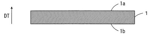
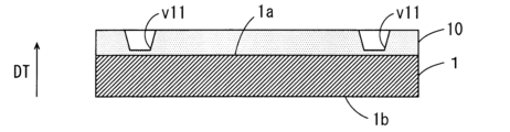
- FIG. 5 is a schematic cross-sectional view for explaining an example of a method for manufacturing the rewiring board of FIG.
- FIG. 6 is a schematic cross-sectional view for explaining an example of a method for manufacturing the rewiring board of FIG.
- FIG. 1 is a schematic cross-sectional view showing the configuration of a rewiring substrate according to an embodiment of the present invention.
- FIG. 2 is a schematic plan view of the rewiring substrate of FIG.
- FIG. 3 is a schematic bottom view of the rewiring substrate of FIG.
- FIG. 7 is a schematic cross-sectional view for explaining an example of a method for manufacturing the rewiring board of FIG.
- FIG. 8 is a schematic cross-sectional view for explaining an example of a method for manufacturing the rewiring board of FIG.
- FIG. 9 is a schematic cross-sectional view for explaining an example of a method for manufacturing the rewiring board of FIG.
- FIG. 10 is a schematic cross-sectional view for explaining an example of a method for manufacturing the rewiring board of FIG.
- FIG. 11 is a schematic cross-sectional view for explaining an example of a method for manufacturing the rewiring board of FIG.
- FIG. 12 is a schematic cross-sectional view for explaining an example of a method for manufacturing the rewiring board of FIG. FIG.
- FIG. 13 is a schematic cross-sectional view for explaining an example of a method for manufacturing the rewiring board of FIG.
- FIG. 14 is a schematic cross-sectional view of a rewiring board showing an example of a state in which an etching solution has entered the inside of the first conductor layer.
- FIG. 15 is a schematic cross-sectional view for explaining a method for manufacturing a rewiring substrate according to a first modified example.
- FIG. 16 is a schematic cross-sectional view for explaining a method for manufacturing a rewiring substrate according to a first modified example.
- FIG. 17 is a schematic cross-sectional view for explaining a method for manufacturing a rewiring substrate according to a first modified example.
- FIG. 18 is a schematic cross-sectional view for explaining a method for manufacturing a rewiring substrate according to a first modified example.
- FIG. 19 is a schematic cross-sectional view for explaining a method for manufacturing a rewiring substrate according to a first modified example.
- FIG. 20 is a diagram for explaining a method for manufacturing a rewiring substrate according to the second modified example.
- FIG. 21 is a diagram for explaining a method for manufacturing a rewiring substrate according to the second modified example.
- FIG. 22 is a diagram for explaining a method for manufacturing a rewiring substrate according to the second modified example.
- FIG. 23 is a diagram for explaining a method for manufacturing a rewiring substrate according to the second modified example.
- FIG. 24 is a schematic cross-sectional view showing the configuration of a rewiring substrate according to another embodiment.
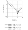
- FIG. 25 is a diagram showing the results of an impedance test on a rewiring board.
- FIG. 26 is a schematic cross-sectional view showing the structure of a mobile terminal used in a simulation for evaluating the heat dissipation property of a semiconductor element.
- FIG. 27 is a diagram showing the results of a number of simulations for evaluating the heat dissipation performance of a semiconductor element.
- a rewired board will be described as an example of a wired circuit board.
- a rewired board is disposed between an electronic component such as a semiconductor element and another wired circuit board such as a rigid printed wiring circuit board (hereinafter abbreviated as rigid board), and serves to convert the pitch between the fine patterns of the electronic components and the coarse patterns of the other wired circuit board.
- a rewired board is also called an interposer board.
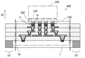
- FIG. 1 is a schematic cross-sectional view showing the configuration of a redistribution substrate according to an embodiment of the present invention.
- FIG. 2 is a schematic plan view of the redistribution substrate 100 of FIG. 1.
- FIG. 3 is a schematic bottom view of the redistribution substrate 100 of FIG. 1.
- FIG. 1 shows a cross section taken along line A-A in FIG. 2 and FIG. 3.
- the redistribution substrate 100 has a first surface (upper surface in this example) 101 and a second surface (lower surface in this example) 102 which face in opposite directions in the thickness direction DT of the redistribution substrate 100.
- the thickness direction DT of the redistribution substrate 100 is indicated by an arrow pointing from bottom to top.
- the rewiring substrate 100 is disposed between the semiconductor element 200 and the rigid substrate 300 in the thickness direction DT.
- a plurality of terminal portions T1 are formed on the first surface 101.
- the semiconductor element 200 is mounted on the first surface 101 of the rewiring substrate 100 to form a semiconductor element mounting substrate 400.
- the semiconductor element mounting substrate 400 is incorporated into an electronic device 800.
- the electronic device 800 is, for example, a mobile terminal such as a smartphone, a tablet terminal, or a wearable terminal.
- the electronic device 800 is, for example, a stationary or notebook personal computer.
- the rewiring substrate 100 generally has a configuration in which multiple conductor layers are formed inside multiple (four in this example) insulating layers arranged in a stacked manner.
- the multiple insulating layers are referred to as the first insulating layer 10, the second insulating layer 20, the third insulating layer 30, and the fourth insulating layer 40, respectively.
- the first insulating layer 10, the second insulating layer 20, the third insulating layer 30, and the fourth insulating layer 40 are arranged in this order in the thickness direction DT of the rewiring substrate 100.
- the via portion 21a is a portion formed inside a through hole h21 (FIG. 8) of the second insulating layer 20, which will be described later.
- the wiring portion 21b is a portion formed in a predetermined pattern on one surface (top surface) of the second insulating layer 20. At least one of the multiple wiring portions 21b is connected to the first conductor layer 11 through the via portion 21a.
- the via portion 31a is a portion formed inside a through hole h31 (FIG. 10) of the third insulating layer 30, which will be described later.
- the wiring portion 31b is a portion formed in a predetermined pattern on one surface (top surface) of the third insulating layer 30. At least one of the multiple wiring portions 31b is connected to the second conductor layer 21 through the via portion 31a.
- the fourth insulating layer 40 functions as a cover insulating layer for protecting the third conductor layer 31 formed on the third insulating layer 30, and one surface (top surface) is exposed to the outside of the rewiring substrate 100. This one surface of the fourth insulating layer 40 constitutes the first surface 101 of the rewiring substrate 100.
- each of the insulating layers (10, 20, 30, 40) is within the above-mentioned preferred range (3 ⁇ m or more and 15 ⁇ m or less) and the thickness of each of the wiring parts 11b, 21b, 31b is within the above-mentioned preferred range (3 ⁇ m or more and 15 ⁇ m or less).
- the sum of the thickness of the first insulating layer 10 and the thickness of the wiring part 11b of the first conductor layer 11 formed on the first insulating layer 10 is 6 ⁇ m or more and 30 ⁇ m or less (see arrow t11 in FIG. 1).
- the roll-to-roll device 500 includes an unwinding section 501, a winding section 502, and a number of processing sections 510, 520, ....
- a roll (unwinding roll) R1 on which a long metal support 1 is wound is prepared and set in the unwinding section 501 of the roll-to-roll device 500.
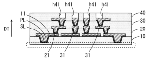
- a plating resist layer of a predetermined pattern is formed on the seed layer SL, and a plating layer PL (FIG. 7) is formed by electrolytic plating on the portions of the seed layer SL exposed through the openings in the plating resist layer.
- the plating resist layer is then removed by etching. Furthermore, the portions of the seed layer SL on which the plating layer PL is not formed are removed by etching.
- one or more first conductor layers 11 having via portions 11a in the through holes h11 and wiring portions 11b on the first insulating layer 10 are formed. Furthermore, one or more first conductor layers 11 having wiring portions 11b on the first insulating layer 10 are formed.
- a seed layer SL is formed on the portions of the second conductor layer 21 exposed inside the through holes h31, the inner circumferential surfaces of the through holes h31, and the third insulating layer 30 in the same manner as when the first conductor layer 11 was formed.
- a plating resist layer of a predetermined pattern is formed on the seed layer SL, and a plating layer PL is formed by electrolytic plating on the portions of the seed layer SL exposed through the openings of the plating resist layer.
- the plating resist layer is also removed by etching.
- the portions of the seed layer SL on which the plating layer PL is not formed are also removed by etching.
- one or more third conductor layers 31 having via portions 31a in the through holes h31 and wiring portions 31b on the third insulating layer 30 are formed.
- One or more third conductor layers 31 having wiring portions 31b on the third insulating layer 30 are also formed.
- a precursor of photosensitive polyimide is newly applied onto the third insulating layer 30 so as to cover the wiring portions 31b of the multiple third conductor layers 31.
- a fourth insulating layer 40 (FIG. 12) is formed on the third insulating layer 30 in the same procedure as that for forming the first insulating layer 10.
- the formed fourth insulating layer 40 is cured.
- multiple through holes h41 are formed in multiple predetermined portions of the fourth insulating layer 40, for example, by laser processing or etching.
- the multiple through holes h41 expose parts of the multiple third conductor layers 31 above the fourth insulating layer 40.
- the formation of the multiple through holes h41 may be performed simultaneously with the formation of the fourth insulating layer 40 on the third insulating layer 30 by using a photosensitive polyimide exposure technique, as in the example of the multiple through holes h11.
- the basic structure of the rewiring substrate 100 of FIG. 1 is completed on the upper surface 1a of the metal support 1.
- the metal support 1 of FIG. 12 on which multiple insulating layers (10, 20, 30, 40) and multiple conductor layers (11, 21, 31) are formed is wound up by the winding roll R2.
- the metal support 1 (laminate of the metal support 1 and the rewiring substrate 100) wound up by the winding roll R2 is set, for example, as a payout roll in another roll-to-roll device. Subsequent processing is performed on the laminate that is paid out from the set payout roll.
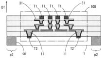
- the metal support 1 is removed from the first insulating layer 10 of the rewiring substrate 100 by wet etching, as shown in FIG. 13.
- the portions of the multiple third conductor layers 31 exposed on the first surface 101 of the rewiring substrate 100 are subjected to surface treatment (plating, etc.) as necessary, to form the multiple terminal portions T1 of FIG. 1.
- the portions of the multiple first conductor layers 11 exposed on the second surface 102 of the rewiring substrate 100 are subjected to surface treatment (plating, etc.) as necessary, to form the multiple terminal portions T2 of FIG. 1.
- the terminal portion T1 may be formed of a part of the third conductor layer 31.
- the terminal portion T2 may be formed of a part of the first conductor layer 11. In these cases, the above-mentioned surface treatment is not necessary for the exposed portions of the third conductor layer 31 and the exposed portions of the first conductor layer 11.
- the portion of the first insulating layer 10 located between the seed layer SL of the first conductor layer 11 and the metal support 1 is formed of photosensitive polyimide. Therefore, during the above-mentioned wet etching, the portion of the first insulating layer 10 located between the seed layer SL of the first conductor layer 11 and the metal support 1 functions as an etching stop layer against the etching solution of the metal support 1.
- the semiconductor element 200 is mounted on the rewiring substrate 100 while the rewiring substrate 100 is supported by the second portion p2 of the metal support 1.
- the rewiring substrate 100 is supported by the second portion p2 of the metal support 1, improving the handleability of the rewiring substrate 100 and stabilizing the mounting operation. As a result, the reliability of the semiconductor element mounting substrate 400 is improved.
- the outer edge portions of the multiple insulating layers (10, 20, 30, 40) are cut from the portion of the insulating layer (10, 20, 30, 40) located on the second portion p2 of the metal support 1. This makes it possible to separate the metal support 1 from the rewiring substrate 100 without using chemicals such as an etching solution that adversely affect the semiconductor element 200.
- the rewiring substrate 100 is manufactured on the metal support 1, which has a higher rigidity than resin or the like. This prevents the intermediate body of the rewiring substrate 100 from being excessively deformed during the manufacturing of the rewiring substrate 100. This improves the reliability of the manufacturing of the rewiring substrate 100.
- a rewiring substrate 100 having a large number of stacked conductor layers can be produced by simply repeating the steps of forming the insulating layer and the conductor layer.
- a plurality of first conductor layers 111 are formed on a portion of the outer surface of the metal support 110 via the coating layer 120.
- Each of the plurality of first conductor layers 111 includes a via portion 111a and wiring portions 111b and 111c.
- a plurality of terminal portions T2 are formed in a portion of the wiring portion 61b of the second conductor layer 61.
- the first insulating layer 50 has openings formed therein for exposing the plurality of terminal portions T2 in the direction in which the second surface 102 faces.
- Each terminal portion T2 may be configured from that portion of the second conductor layer 61, or may be formed by performing a surface treatment on that portion of the second conductor layer 61.
- the rewiring substrate 100 of FIG. 24 having the above configuration is generally fabricated as follows. First, a metal support 110 is prepared, and a plurality of through holes h111 are formed in a predetermined portion of the metal support 110. A coating layer 120 is formed over the entire outer surface of the metal support 110. After that, a first conductor layer 111 is formed on a predetermined portion of the outer surface of the metal support 110 via the coating layer 120.
- the metal support 110 has a higher thermal conductivity than the multiple insulating layers (50, 60, 70, 80). Therefore, when the semiconductor element 200 is mounted on the rewiring substrate 100, the metal support 110 is likely to receive heat generated by the semiconductor element 200. Therefore, the metal support 110 functions as a heat dissipation member for the semiconductor element 200.
- the linear expansion coefficient of the metal support 110 at temperatures from 25°C to 200°C is 0 ppm/K to 25 ppm/K.
- the metal support 110 is prevented from deforming significantly as the temperature of the rewiring substrate 100 changes. This improves the reliability of the rewiring substrate 100.
- a semiconductor element 200 is mounted on the first surface 101 of the rewiring substrate 100 to form a semiconductor element mounting substrate 400.
- the semiconductor element mounting substrate 400 is incorporated into an electronic device 800.
- the multiple conductor layers (11, 21, 31, 61, 71) are examples of multiple conductor layers
- the semiconductor element 200 and the rigid substrate 300 are examples of electrical elements
- the tips of the multiple columnar joints 220 of the semiconductor element 200 and the multiple electrode pads 301 of the rigid substrate 300 are examples of connection terminals
- the terminal portion T1 of the redistribution substrate 100 is an example of a first connected portion
- the terminal portion T2 of the redistribution substrate 100 is an example of a second connected portion
- any of the multiple conductor layers (11, 21, 31, 61, 71) is an example of a first conductor layer.
- the semiconductor element 200 is an example of a first electrical element
- the rigid substrate 300 is an example of a second electrical element
- the second insulating layer 20 is an example of a second insulating layer
- the third insulating layer 30 is an example of a third insulating layer
- the second conductor layer 21 is an example of a second conductor layer
- the third conductor layer 31 is an example of a third conductor layer
- the multiple insulating layers (10, 20, 30, 60, 70) are an example of multiple base insulating layers
- the multiple insulating layers (40, 50, 80) are an example of cover insulating layers.
- the metal support 1 is an example of a metal support
- any of the multiple insulating layers (60, 70) is an example of a second insulating layer
- any of the multiple conductor layers (61, 71) is an example of a second conductor layer
- the solder S is an example of a joining member
- the opposing surface 211 is an example of an opposing surface
- the columnar joint 220 is an example of a columnar joint
- the semiconductor element mounting board 400 is an example of an electrical element mounting board
- the electronic device 800 is an example of an electronic device.
- Example 1 a rewiring substrate 100 having basically the same configuration as the rewiring substrate 100 in FIG. 1.
- multiple insulating layers (10, 20, 30, 40) were produced from photosensitive polyimide.
- Each insulating layer had a thickness of 5 ⁇ m.
- each insulating layer had a dielectric constant of 3.3 and a dielectric dissipation factor of 0.007.
- each of the multiple conductor layers (11, 21, 31) was formed from copper.
- Each conductor layer had a thickness of 5 ⁇ m.
- the inventors also fabricated a rewiring board as Comparative Example 1, which had the same configuration as the rewiring board 100 of Example 1, except for the thickness and material of each part.
- the multiple insulating layers were fabricated using a material (MEGTRON GX R-1515A manufactured by Panasonic) different from the photosensitive polyimide of Example 1.
- the thickness of each insulating layer was 30 ⁇ m.
- the dielectric constant of each insulating layer was 4.7, and the dielectric tangent of each insulating layer was 0.011.
- each of the multiple conductor layers was formed from copper.
- the thickness of each conductor layer was 15 ⁇ m.
- Example 11 a rewiring board model having the configuration of FIG. 1 and a thickness of the rewiring board 100 (the distance between the first surface 101 and the second surface 102 in the thickness direction DT) of 40 ⁇ m. Furthermore, the inventors assumed, as Example 12, a rewiring board model having the configuration of FIG. 24 and a thickness of the rewiring board 100 (the distance between the first surface 101 and the second surface 102 in the thickness direction DT) of 65 ⁇ m. Furthermore, the inventors assumed, as Comparative Example 11, a rewiring board model having the configuration of FIG.
- the mobile terminal 900 has a configuration in which multiple types of components 901, such as a battery, are housed together with a rigid substrate 300A inside a casing 910.
- a rewiring substrate 100 is connected to the rigid substrate 300A via a bonding member 390.
- a semiconductor element 200 is mounted on the rewiring substrate 100.
- the rewiring substrate 100 and the semiconductor element 200 form a semiconductor element mounting substrate 400.
- the bonding member 390 includes solder.
- the semiconductor element mounting substrate 400 is covered with a sealing resin 490.
- a heat dissipation member 491 is further attached to the sealing resin 490. The heat dissipation member 491 is in contact with some of the multiple types of components 901 housed inside the casing 910.
- a predetermined point located at the connection between rigid board 300A and semiconductor element mounting board 400 is referred to as point of interest tp.
- the temperature change of point of interest tp during a certain period of time after a specific program is started on mobile terminal 900 is calculated by simulation.
- the temperature change at the point of interest tp during a certain period of time after a specific program is started on the mobile terminal 900 is calculated by simulation.
- the temperature change at the point of interest tp during a certain period of time after a specific program is started on the mobile terminal 900 is calculated by simulation.
- the simulation results corresponding to the rewiring substrate model of Example 11 are shown by black circles and a solid line.
- the simulation results corresponding to the rewiring substrate model of Comparative Example 11 are shown by triangles and a dotted line.
- the simulation results corresponding to the rewiring substrate model of Example 12 were nearly identical to the simulation results corresponding to the rewiring substrate model of Example 11, to the extent that the difference could not be seen on the graph of Figure 27. Therefore, the simulation results corresponding to the rewiring substrate model of Example 12 are not shown in the figure.
- the temperature of the point of interest tp reaches 50°C 160 seconds after a specific program is started.
- the temperature of the point of interest tp reaches 50°C 140 seconds after a specific program is started.
- the printed circuit board according to the 1st embodiment is A wired circuit board having a first surface and a second surface facing in opposite directions in a thickness direction, A plurality of insulating layers including a first insulating layer, the insulating layers being stacked in the thickness direction; a plurality of conductor layers formed on any one of the plurality of insulating layers; a first connected portion and a second connected portion configured to be connectable to a connection terminal of an electrical element; the first connected portion is formed on the first surface so as to be electrically connected to the plurality of conductor layers and exposed in a direction toward which the first surface faces; the second connected portion is formed on the second surface so as to be electrically connected to the plurality of conductor layers and exposed in a direction toward the second surface; the plurality of conductor layers includes a first conductor layer formed on the first insulating layer; The sum of the thickness of the portion of the first insulating layer where the first conductor layer is formed and the thickness of the first conductor layer is 30 ⁇ m
- connection terminal of the electrical element can be connected to a first connected portion on the first surface. Also, a connection terminal of the electrical element can be connected to a second connected portion on the second surface. Therefore, it is easy to mount the electrical element on the wired circuit board.
- the overall thickness of the wired circuit board can be made smaller than when the sum of the thickness of the portion of the first insulating layer where the first conductor layer is formed and the thickness of the first conductor layer is greater than 30 ⁇ m. In other words, the wired circuit board can be made thinner.
- Each of the first electrical element and the second electrical element is, for example, an electronic component such as a semiconductor element or a rigid printed wiring circuit board, and has a plurality of connection terminals.
- the wiring circuit board as a rewiring board, converts the pitch between the plurality of connection terminals of the first electrical element and the pitch between the plurality of connection terminals of the second electrical element.
- the plurality of insulating layers includes a second insulating layer and a third insulating layer; the plurality of conductor layers include a second conductor layer formed on the second insulating layer and a third conductor layer formed on the third insulating layer; the sum of a thickness of the portion of the second insulating layer on which the second conductor layer is formed and a thickness of the second conductor layer is 30 ⁇ m or less; The sum of a thickness of the portion of the third insulating layer on which the third conductor layer is formed and a thickness of the third conductor layer may be 30 ⁇ m or less.
- the thickness of the wiring circuit board having a structure in which three or more insulating layers are stacked can be reduced.
- the wiring circuit board can be made even thinner.
- the plurality of insulating layers includes a cover insulating layer formed on the plurality of base insulating layers arranged in a stacked manner,
- the insulating cover layer may have a thickness of 3 ⁇ m or more and 15 ⁇ m or less.
- the wiring circuit board can be made even thinner.
- each of the plurality of insulating layers is 3 ⁇ m or more and 15 ⁇ m or less, The thickness of each of the plurality of conductor layers may be not less than 3 ⁇ m and not more than 15 ⁇ m.
- the semiconductor device may further include a metal support for supporting the plurality of insulating layers and the plurality of conductor layers.
- the metal support has a higher thermal conductivity than the insulating layer. Therefore, when an electrical element is mounted on the wiring circuit board, the metal support is more likely to receive heat generated by the electrical element. Therefore, the metal support functions as a heat dissipation member for the electrical element.
- the plurality of insulating layers includes a second insulating layer; the plurality of conductor layers includes a second conductor layer formed on the second insulating layer;
- the metal support may be located between the first insulating layer and the first conductor layer and between the second insulating layer and the second conductor layer in the thickness direction.
- the electrical component mounting board also includes the above-mentioned wiring circuit board.
- the electrical component mounting board can be easily manufactured, and the impedance of the wiring formed by the first conductor layer can be reduced and heat dissipation of the mounted electrical components can be ensured.
- the bonding material may include solder, in which case a highly reliable electrical component mounting board can be produced using a general-purpose bonding material.
- the electronic device according to clause 15 includes the above-mentioned electrical component mounting board.
- the overall thickness of the wired circuit board can be made smaller than when the sum of the thickness of the portion of the first insulating layer where the first conductor layer is formed and the thickness of the first conductor layer is greater than 30 ⁇ m. In other words, the wired circuit board can be made thinner.
- a method for manufacturing an electrical component mounting board includes the steps of: A step of producing the printed circuit board by the manufacturing method according to item 16 or 17; and mounting an electrical element having a connection terminal on the first surface of the printed circuit board produced by the manufacturing method.
- the mounting step includes: using a joining member to join the connection terminal of the electrical element and the first connected portion of the wired circuit board;
- the electrical element comprises: an opposing surface that faces the wired circuit board when mounted on the wired circuit board; A columnar joint formed to protrude a certain length from the opposing surface, The connection terminal is formed at the tip of the columnar joint.
- the opposing surfaces of the electrical elements can be placed opposite the first surface of the wired circuit board, and the connection terminals of the electrical elements can be connected to the first connected portions of the wired circuit board.
- the opposing surfaces of the electrical elements can be placed opposite the second surface of the wired circuit board, and the connection terminals of the electrical elements can be connected to the second connected portions of the wired circuit board.
- the connection terminals of the electrical elements are formed at the tips of the columnar joints, the connection work is easier than when the connection terminals are formed on a flat surface.
- the reliability of the connection using the joining member is improved.
- the electrical component mounting board also includes the above-mentioned wiring circuit board.
- the electrical component mounting board can be easily manufactured, and the impedance of the wiring formed by the first conductor layer can be reduced and heat dissipation of the mounted electrical components can be ensured.
Landscapes
- Engineering & Computer Science (AREA)
- Microelectronics & Electronic Packaging (AREA)
- Manufacturing & Machinery (AREA)
- Production Of Multi-Layered Print Wiring Board (AREA)
- Parts Printed On Printed Circuit Boards (AREA)
- Chemical & Material Sciences (AREA)
- Materials Engineering (AREA)
- Electric Connection Of Electric Components To Printed Circuits (AREA)
Priority Applications (2)
| Application Number | Priority Date | Filing Date | Title |
|---|---|---|---|
| KR1020257024108A KR20250130328A (ko) | 2022-12-28 | 2023-12-28 | 배선 회로 기판, 전기적 요소 실장 기판, 전자 기기, 배선 회로 기판의 제조 방법 및 전기적 요소 실장 기판의 제조 방법 |
| CN202380088894.1A CN120418955A (zh) | 2022-12-28 | 2023-12-28 | 布线电路基板、电气要素安装基板、电子设备、布线电路基板的制造方法、以及电气要素安装基板的制造方法 |
Applications Claiming Priority (2)
| Application Number | Priority Date | Filing Date | Title |
|---|---|---|---|
| JP2022211280A JP2024094620A (ja) | 2022-12-28 | 2022-12-28 | 配線回路基板、電気的要素実装基板、配線回路基板の製造方法および電気的要素実装基板の製造方法 |
| JP2022-211280 | 2022-12-28 |
Publications (1)
| Publication Number | Publication Date |
|---|---|
| WO2024143520A1 true WO2024143520A1 (ja) | 2024-07-04 |
Family
ID=91717949
Family Applications (1)
| Application Number | Title | Priority Date | Filing Date |
|---|---|---|---|
| PCT/JP2023/047178 Ceased WO2024143520A1 (ja) | 2022-12-28 | 2023-12-28 | 配線回路基板、電気的要素実装基板、電子機器、配線回路基板の製造方法および電気的要素実装基板の製造方法 |
Country Status (5)
| Country | Link |
|---|---|
| JP (1) | JP2024094620A (https=) |
| KR (1) | KR20250130328A (https=) |
| CN (1) | CN120418955A (https=) |
| TW (1) | TW202435372A (https=) |
| WO (1) | WO2024143520A1 (https=) |
Citations (7)
| Publication number | Priority date | Publication date | Assignee | Title |
|---|---|---|---|---|
| JP2000022052A (ja) * | 1998-06-30 | 2000-01-21 | Casio Comput Co Ltd | 半導体装置及びその製造方法 |
| JP2000349198A (ja) * | 1999-04-02 | 2000-12-15 | Nitto Denko Corp | チップサイズパッケージ用インターポーザ及びその製造方法と中間部材 |
| JP2002223050A (ja) * | 2001-01-29 | 2002-08-09 | Hitachi Metals Ltd | 複合金属板、ビルドアップコア基板、ビルドアップ配線基板、及びその製造方法 |
| JP2006186321A (ja) * | 2004-12-01 | 2006-07-13 | Shinko Electric Ind Co Ltd | 回路基板の製造方法及び電子部品実装構造体の製造方法 |
| JP2016039285A (ja) * | 2014-08-08 | 2016-03-22 | イビデン株式会社 | プリント配線板の製造方法 |
| JP2018207082A (ja) * | 2017-06-09 | 2018-12-27 | イビデン株式会社 | リジッドフレキシブル配線板およびその製造方法 |
| JP2019068032A (ja) * | 2017-04-10 | 2019-04-25 | 日東電工株式会社 | 撮像素子実装基板、その製造方法、および、実装基板集合体 |
-
2022
- 2022-12-28 JP JP2022211280A patent/JP2024094620A/ja active Pending
-
2023
- 2023-12-28 CN CN202380088894.1A patent/CN120418955A/zh active Pending
- 2023-12-28 TW TW112151350A patent/TW202435372A/zh unknown
- 2023-12-28 WO PCT/JP2023/047178 patent/WO2024143520A1/ja not_active Ceased
- 2023-12-28 KR KR1020257024108A patent/KR20250130328A/ko active Pending
Patent Citations (7)
| Publication number | Priority date | Publication date | Assignee | Title |
|---|---|---|---|---|
| JP2000022052A (ja) * | 1998-06-30 | 2000-01-21 | Casio Comput Co Ltd | 半導体装置及びその製造方法 |
| JP2000349198A (ja) * | 1999-04-02 | 2000-12-15 | Nitto Denko Corp | チップサイズパッケージ用インターポーザ及びその製造方法と中間部材 |
| JP2002223050A (ja) * | 2001-01-29 | 2002-08-09 | Hitachi Metals Ltd | 複合金属板、ビルドアップコア基板、ビルドアップ配線基板、及びその製造方法 |
| JP2006186321A (ja) * | 2004-12-01 | 2006-07-13 | Shinko Electric Ind Co Ltd | 回路基板の製造方法及び電子部品実装構造体の製造方法 |
| JP2016039285A (ja) * | 2014-08-08 | 2016-03-22 | イビデン株式会社 | プリント配線板の製造方法 |
| JP2019068032A (ja) * | 2017-04-10 | 2019-04-25 | 日東電工株式会社 | 撮像素子実装基板、その製造方法、および、実装基板集合体 |
| JP2018207082A (ja) * | 2017-06-09 | 2018-12-27 | イビデン株式会社 | リジッドフレキシブル配線板およびその製造方法 |
Also Published As
| Publication number | Publication date |
|---|---|
| CN120418955A (zh) | 2025-08-01 |
| JP2024094620A (ja) | 2024-07-10 |
| TW202435372A (zh) | 2024-09-01 |
| KR20250130328A (ko) | 2025-09-01 |
Similar Documents
| Publication | Publication Date | Title |
|---|---|---|
| US9723729B2 (en) | Printed wiring board | |
| US9258899B2 (en) | Method of fabricating a wiring board | |
| CN101548378A (zh) | 半导体器件及其制造方法 | |
| US8120148B2 (en) | Package structure with embedded die and method of fabricating the same | |
| KR20110029465A (ko) | 인쇄회로기판 및 그의 제조 방법 | |
| TWI360213B (en) | Chip package carrier, chip package and method for | |
| JP7539820B2 (ja) | 配線基板及び半導体装置 | |
| JP2018082084A (ja) | プリント配線板およびプリント配線板の製造方法 | |
| US11935822B2 (en) | Wiring substrate having metal post offset from conductor pad and method for manufacturing wiring substrate | |
| US20220013455A1 (en) | Wiring substrate and method for manufacturing wiring substrate | |
| KR102797259B1 (ko) | 반도체 장치 및 반도체 장치의 제조 방법 | |
| WO2024143520A1 (ja) | 配線回路基板、電気的要素実装基板、電子機器、配線回路基板の製造方法および電気的要素実装基板の製造方法 | |
| US9041166B2 (en) | Manufacturing method of circuit structure | |
| JP2024094622A (ja) | 配線回路基板およびその製造方法 | |
| US11749596B2 (en) | Wiring substrate | |
| JP2024094621A (ja) | 電気的要素実装基板の製造方法 | |
| JP4514538B2 (ja) | 回路装置およびその製造方法 | |
| WO2024224941A1 (ja) | 配線回路基板、電気的要素実装基板、電子機器および配線回路基板の製造方法 | |
| JP2025008669A (ja) | 配線回路基板および配線回路基板の製造方法 | |
| WO2023080097A1 (ja) | 再配線基板およびその製造方法 | |
| JP2023069418A (ja) | 再配線基板およびその製造方法 | |
| KR101113889B1 (ko) | 전자 소자를 내장하는 회로기판 및 회로기판의 제조 방법 | |
| JP2025039435A (ja) | 配線回路基板および配線回路基板集合体シート | |
| CN116779578A (zh) | 电子封装件及其封装基板与制法 | |
| JP2008124260A (ja) | 多層配線基板及びその製造方法 |
Legal Events
| Date | Code | Title | Description |
|---|---|---|---|
| 121 | Ep: the epo has been informed by wipo that ep was designated in this application |
Ref document number: 23912297 Country of ref document: EP Kind code of ref document: A1 |
|
| WWE | Wipo information: entry into national phase |
Ref document number: 202380088894.1 Country of ref document: CN |
|
| ENP | Entry into the national phase |
Ref document number: 1020257024108 Country of ref document: KR Free format text: ST27 STATUS EVENT CODE: A-0-1-A10-A15-NAP-PA0105 (AS PROVIDED BY THE NATIONAL OFFICE) |
|
| WWE | Wipo information: entry into national phase |
Ref document number: 1020257024108 Country of ref document: KR |
|
| NENP | Non-entry into the national phase |
Ref country code: DE |
|
| WWP | Wipo information: published in national office |
Ref document number: 202380088894.1 Country of ref document: CN |
|
| 122 | Ep: pct application non-entry in european phase |
Ref document number: 23912297 Country of ref document: EP Kind code of ref document: A1 |