WO2024142638A1 - 半導体装置および半導体装置の製造方法 - Google Patents
半導体装置および半導体装置の製造方法 Download PDFInfo
- Publication number
- WO2024142638A1 WO2024142638A1 PCT/JP2023/041006 JP2023041006W WO2024142638A1 WO 2024142638 A1 WO2024142638 A1 WO 2024142638A1 JP 2023041006 W JP2023041006 W JP 2023041006W WO 2024142638 A1 WO2024142638 A1 WO 2024142638A1
- Authority
- WO
- WIPO (PCT)
- Prior art keywords
- film
- semiconductor substrate
- contact
- interlayer insulating
- insulating film
- Prior art date
- Legal status (The legal status is an assumption and is not a legal conclusion. Google has not performed a legal analysis and makes no representation as to the accuracy of the status listed.)
- Ceased
Links
Images







Classifications
-
- H—ELECTRICITY
- H10—SEMICONDUCTOR DEVICES; ELECTRIC SOLID-STATE DEVICES NOT OTHERWISE PROVIDED FOR
- H10D—INORGANIC ELECTRIC SEMICONDUCTOR DEVICES
- H10D64/00—Electrodes of devices having potential barriers
- H10D64/01—Manufacture or treatment
- H10D64/013—Manufacture or treatment of electrodes having a conductor capacitively coupled to a semiconductor by an insulator
- H10D64/01302—Manufacture or treatment of electrodes having a conductor capacitively coupled to a semiconductor by an insulator the insulator being formed after the semiconductor body, the semiconductor being silicon
- H10D64/01304—Manufacture or treatment of electrodes having a conductor capacitively coupled to a semiconductor by an insulator the insulator being formed after the semiconductor body, the semiconductor being silicon characterised by the conductor
- H10D64/01306—Manufacture or treatment of electrodes having a conductor capacitively coupled to a semiconductor by an insulator the insulator being formed after the semiconductor body, the semiconductor being silicon characterised by the conductor the conductor comprising a layer of silicon contacting the insulator, e.g. polysilicon
- H10D64/01308—Manufacture or treatment of electrodes having a conductor capacitively coupled to a semiconductor by an insulator the insulator being formed after the semiconductor body, the semiconductor being silicon characterised by the conductor the conductor comprising a layer of silicon contacting the insulator, e.g. polysilicon the conductor further comprising a non-elemental silicon additional conductive layer, e.g. a metal silicide layer formed by the reaction of silicon with an implanted metal
- H10D64/01312—Manufacture or treatment of electrodes having a conductor capacitively coupled to a semiconductor by an insulator the insulator being formed after the semiconductor body, the semiconductor being silicon characterised by the conductor the conductor comprising a layer of silicon contacting the insulator, e.g. polysilicon the conductor further comprising a non-elemental silicon additional conductive layer, e.g. a metal silicide layer formed by the reaction of silicon with an implanted metal the additional layer comprising a metal or metal silicide formed by deposition, i.e. without a silicidation reaction, e.g. sputter deposition
-
- H—ELECTRICITY
- H10—SEMICONDUCTOR DEVICES; ELECTRIC SOLID-STATE DEVICES NOT OTHERWISE PROVIDED FOR
- H10D—INORGANIC ELECTRIC SEMICONDUCTOR DEVICES
- H10D30/00—Field-effect transistors [FET]
- H10D30/01—Manufacture or treatment
- H10D30/021—Manufacture or treatment of FETs having insulated gates [IGFET]
-
- H—ELECTRICITY
- H10—SEMICONDUCTOR DEVICES; ELECTRIC SOLID-STATE DEVICES NOT OTHERWISE PROVIDED FOR
- H10D—INORGANIC ELECTRIC SEMICONDUCTOR DEVICES
- H10D30/00—Field-effect transistors [FET]
- H10D30/60—Insulated-gate field-effect transistors [IGFET]
-
- H—ELECTRICITY
- H10—SEMICONDUCTOR DEVICES; ELECTRIC SOLID-STATE DEVICES NOT OTHERWISE PROVIDED FOR
- H10D—INORGANIC ELECTRIC SEMICONDUCTOR DEVICES
- H10D30/00—Field-effect transistors [FET]
- H10D30/60—Insulated-gate field-effect transistors [IGFET]
- H10D30/64—Double-diffused metal-oxide semiconductor [DMOS] FETs
- H10D30/66—Vertical DMOS [VDMOS] FETs
- H10D30/668—Vertical DMOS [VDMOS] FETs having trench gate electrodes, e.g. UMOS transistors
-
- H—ELECTRICITY
- H10—SEMICONDUCTOR DEVICES; ELECTRIC SOLID-STATE DEVICES NOT OTHERWISE PROVIDED FOR
- H10D—INORGANIC ELECTRIC SEMICONDUCTOR DEVICES
- H10D64/00—Electrodes of devices having potential barriers
- H10D64/01—Manufacture or treatment
- H10D64/011—Manufacture or treatment of electrodes ohmically coupled to a semiconductor
-
- H—ELECTRICITY
- H10—SEMICONDUCTOR DEVICES; ELECTRIC SOLID-STATE DEVICES NOT OTHERWISE PROVIDED FOR
- H10D—INORGANIC ELECTRIC SEMICONDUCTOR DEVICES
- H10D64/00—Electrodes of devices having potential barriers
- H10D64/01—Manufacture or treatment
- H10D64/011—Manufacture or treatment of electrodes ohmically coupled to a semiconductor
- H10D64/0111—Manufacture or treatment of electrodes ohmically coupled to a semiconductor to Group IV semiconductors
- H10D64/0112—Manufacture or treatment of electrodes ohmically coupled to a semiconductor to Group IV semiconductors using conductive layers comprising silicides
-
- H—ELECTRICITY
- H10—SEMICONDUCTOR DEVICES; ELECTRIC SOLID-STATE DEVICES NOT OTHERWISE PROVIDED FOR
- H10D—INORGANIC ELECTRIC SEMICONDUCTOR DEVICES
- H10D64/00—Electrodes of devices having potential barriers
- H10D64/20—Electrodes characterised by their shapes, relative sizes or dispositions
- H10D64/23—Electrodes carrying the current to be rectified, amplified, oscillated or switched, e.g. sources, drains, anodes or cathodes
-
- H—ELECTRICITY
- H10—SEMICONDUCTOR DEVICES; ELECTRIC SOLID-STATE DEVICES NOT OTHERWISE PROVIDED FOR
- H10P—GENERIC PROCESSES OR APPARATUS FOR THE MANUFACTURE OR TREATMENT OF DEVICES COVERED BY CLASS H10
- H10P34/00—Irradiation with electromagnetic or particle radiation of wafers, substrates or parts of devices
- H10P34/40—Irradiation with electromagnetic or particle radiation of wafers, substrates or parts of devices with high-energy radiation
-
- H—ELECTRICITY
- H10—SEMICONDUCTOR DEVICES; ELECTRIC SOLID-STATE DEVICES NOT OTHERWISE PROVIDED FOR
- H10P—GENERIC PROCESSES OR APPARATUS FOR THE MANUFACTURE OR TREATMENT OF DEVICES COVERED BY CLASS H10
- H10P36/00—Gettering within semiconductor bodies
-
- H—ELECTRICITY
- H10—SEMICONDUCTOR DEVICES; ELECTRIC SOLID-STATE DEVICES NOT OTHERWISE PROVIDED FOR
- H10P—GENERIC PROCESSES OR APPARATUS FOR THE MANUFACTURE OR TREATMENT OF DEVICES COVERED BY CLASS H10
- H10P95/00—Generic processes or apparatus for manufacture or treatments not covered by the other groups of this subclass
- H10P95/90—Thermal treatments, e.g. annealing or sintering
-
- H—ELECTRICITY
- H10—SEMICONDUCTOR DEVICES; ELECTRIC SOLID-STATE DEVICES NOT OTHERWISE PROVIDED FOR
- H10W—GENERIC PACKAGES, INTERCONNECTIONS, CONNECTORS OR OTHER CONSTRUCTIONAL DETAILS OF DEVICES COVERED BY CLASS H10
- H10W20/00—Interconnections in chips, wafers or substrates
- H10W20/01—Manufacture or treatment
-
- H—ELECTRICITY
- H10—SEMICONDUCTOR DEVICES; ELECTRIC SOLID-STATE DEVICES NOT OTHERWISE PROVIDED FOR
- H10W—GENERIC PACKAGES, INTERCONNECTIONS, CONNECTORS OR OTHER CONSTRUCTIONAL DETAILS OF DEVICES COVERED BY CLASS H10
- H10W20/00—Interconnections in chips, wafers or substrates
- H10W20/01—Manufacture or treatment
- H10W20/031—Manufacture or treatment of conductive parts of the interconnections
- H10W20/032—Manufacture or treatment of conductive parts of the interconnections of conductive barrier, adhesion or liner layers
- H10W20/038—Manufacture or treatment of conductive parts of the interconnections of conductive barrier, adhesion or liner layers covering conductive structures
-
- H—ELECTRICITY
- H10—SEMICONDUCTOR DEVICES; ELECTRIC SOLID-STATE DEVICES NOT OTHERWISE PROVIDED FOR
- H10W—GENERIC PACKAGES, INTERCONNECTIONS, CONNECTORS OR OTHER CONSTRUCTIONAL DETAILS OF DEVICES COVERED BY CLASS H10
- H10W20/00—Interconnections in chips, wafers or substrates
- H10W20/01—Manufacture or treatment
- H10W20/031—Manufacture or treatment of conductive parts of the interconnections
- H10W20/032—Manufacture or treatment of conductive parts of the interconnections of conductive barrier, adhesion or liner layers
- H10W20/047—Manufacture or treatment of conductive parts of the interconnections of conductive barrier, adhesion or liner layers by introducing additional elements therein
- H10W20/048—Manufacture or treatment of conductive parts of the interconnections of conductive barrier, adhesion or liner layers by introducing additional elements therein by using plasmas or gaseous environments, e.g. by nitriding
-
- H—ELECTRICITY
- H10—SEMICONDUCTOR DEVICES; ELECTRIC SOLID-STATE DEVICES NOT OTHERWISE PROVIDED FOR
- H10W—GENERIC PACKAGES, INTERCONNECTIONS, CONNECTORS OR OTHER CONSTRUCTIONAL DETAILS OF DEVICES COVERED BY CLASS H10
- H10W20/00—Interconnections in chips, wafers or substrates
- H10W20/40—Interconnections external to wafers or substrates, e.g. back-end-of-line [BEOL] metallisations or vias connecting to gate electrodes
Definitions
- Patent Documents 1 to 4 the Ti film contained in the laminated structure of the front electrode inhibits the effect of hydrogen annealing to repair crystal damage in the semiconductor substrate. Also, in Patent Document 4, the volume expansion of the TiSi film due to silicidation increases the stress locally generated in the semiconductor substrate. In Patent Document 5, chlorine (Cl) contained in the gas composition introduced by PECVD to form the TiSi film causes corrosion of the semiconductor substrate.
- the purpose of this disclosure is to provide a highly reliable semiconductor device and a method for manufacturing a semiconductor device in order to resolve the problems associated with the conventional technology described above.
- a method for manufacturing a semiconductor device is as follows: A first step is performed in which a second semiconductor region of a second conductivity type is formed in a surface region of the front surface of a semiconductor substrate, the second semiconductor region being in contact with a first semiconductor region of a first conductivity type inside the semiconductor substrate, and an element structure including a pn junction between the second semiconductor region and the first semiconductor region is formed. A second step is performed in which an interlayer insulating film is formed on the front surface of the semiconductor substrate to cover the element structure. A third step is performed in which a contact hole is formed that penetrates the interlayer insulating film in the depth direction and reaches the semiconductor substrate. A fourth step is performed in which a contact structure is formed in the contact hole and in contact with the semiconductor substrate. A fifth step is performed in which a first electrode is formed that is electrically connected to the second semiconductor region via the contact structure.
- a first annealing step is performed to repair crystal damage to the semiconductor substrate by heat treatment in a hydrogen atmosphere.
- the fourth step includes first to third deposition steps.
- a titanium silicide film is deposited by sputtering to cover the entire surface of the interlayer insulating film and to contact the semiconductor substrate in the contact hole.
- a titanium nitride film is deposited by sputtering on the surface of the titanium silicide film.
- a metal plug is embedded on the titanium nitride film inside the contact hole.
- the contact structure is formed, consisting of the titanium silicide film, the titanium nitride film, and the metal plug.
- the semiconductor device and the method for manufacturing the semiconductor device disclosed herein have the effect of improving reliability.
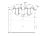
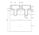
- FIG. 1 is a cross-sectional view showing a structure of a semiconductor device according to a first embodiment.
- FIG. 2 is a cross-sectional view showing a state during the manufacturing process of the semiconductor device according to the first embodiment.
- FIG. 3 is a cross-sectional view showing a state during the manufacturing process of the semiconductor device according to the first embodiment.
- FIG. 4 is a cross-sectional view showing a state during the manufacturing process of the semiconductor device according to the first embodiment.
- FIG. 5 is a cross-sectional view showing a state during the manufacturing process of the semiconductor device according to the first embodiment.
- FIG. 6 is a cross-sectional view showing a state during the manufacturing process of the semiconductor device according to the first embodiment.
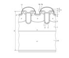
- FIG. 7 is a cross-sectional view showing the structure of a semiconductor device according to the second embodiment.
- FIG. 8 is a cross-sectional view showing a state during the manufacturing process of the semiconductor device according to the second embodiment.
- FIG. 9 is a diagram showing the relationship between the degree of recovery from crystal damage of a semiconductor substrate caused by hydrogen annealing and the barrier metal.
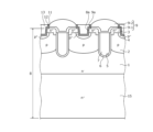
- FIG. 10 is a cross-sectional view showing the structure of Comparative Example 1.
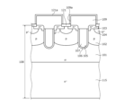
- FIG. 11 is a cross-sectional view showing the structure of the second comparative example.
- FIG. 12 is a cross-sectional view showing a state during the manufacturing process of Comparative Example 2.
- FIG. 13 is a cross-sectional view showing a state during the manufacturing process of Comparative Example 2.
- FIG. 10 is a cross-sectional view showing the structure of Comparative Example 1.
- FIG. 11 is a cross-sectional view showing the structure of the second comparative example.
- FIG. 12 is a cross-sectional view showing a state during the manufacturing process
- FIG. 14 is a cross-sectional view showing a state during the production of Comparative Example 2.
- FIG. 15 is a cross-sectional view showing a state during the production of Comparative Example 2.
- FIG. 16 is a cross-sectional view showing a state during the production of Comparative Example 2.
- FIG. 17 is a cross-sectional view showing a state during the manufacturing process of Comparative Example 2.
- FIG. 18 is a cross-sectional view showing a state during the manufacturing process of Comparative Example 2.
- a semiconductor device is as follows: A first semiconductor region of a first conductivity type is provided inside a semiconductor substrate. A second semiconductor region of a second conductivity type is provided between a front surface of the semiconductor substrate and the first semiconductor region. An element structure including a pn junction between the second semiconductor region and the first semiconductor region is provided on the front surface side of the semiconductor substrate. An interlayer insulating film is provided on the front surface of the semiconductor substrate. The interlayer insulating film covers the element structure. A contact hole penetrates the interlayer insulating film in the depth direction to reach the semiconductor substrate. A contact structure contacts the semiconductor substrate at the contact hole.
- the stress applied to the interlayer insulating film and the semiconductor substrate is uniform on the sidewalls of the contact hole and the sidewalls of the contact trench.
- the above disclosure makes it possible to suppress damage to the interlayer insulating film caused by ultrasonic vibrations during wire bonding to the first electrode.
- the first electrode and the semiconductor substrate are electrically connected via a TiSix film (titanium silicide film), thereby reducing the contact resistance between the first electrode and the semiconductor substrate.
- a TiSix film titanium silicide film
- special high-temperature heat treatment such as silicidation is not required to form the TiSix film. This makes it possible to suppress localized stress in the semiconductor substrate.
- a Ti film that adsorbs hydrogen is not formed on the surface of the interlayer insulating film, it is easy to recover from crystal damage in the semiconductor substrate caused by hydrogen annealing.
- a Ti film is not formed on the surface of the interlayer insulating film, it is possible to prevent a decrease in adhesion with the interlayer insulating film due to a reaction between the material gas and the Ti film when forming a metal plug.
- the contact area between the TiSix film and the semiconductor substrate is increased, making it possible to suppress an increase in the contact resistance between the first electrode and the semiconductor substrate.
- the above disclosure makes it possible to improve the embeddability of metal plugs in contact trenches.
- the fourth step further includes a removal step of etching back the titanium nitride film and the titanium silicide film using the metal plug as a mask to expose the upper surface of the interlayer insulating film.
- the first electrode may be formed on the upper surface of the interlayer insulating film in contact with the interlayer insulating film.
- a TiSix film which is a material film of the TiSix film, is formed to cover the entire surface of the interlayer insulating film, but this Ti film is prone to absorbing hydrogen, hindering the effect of hydrogen annealing for recovering crystal damage of the semiconductor substrate. Therefore, even if hydrogen annealing is performed, it is difficult to recover characteristics such as gate threshold voltage.
- FIG. 1 is a cross-sectional view showing the structure of a semiconductor device according to the first embodiment.
- the semiconductor substrate 8 is, for example, an n - type Si bulk substrate that becomes the n - type drift region (first semiconductor region) 1, or a Si substrate in which an n - type epitaxial layer that becomes the n - type drift region 1 is laminated on an n + type starting substrate (Si bulk substrate) that becomes the n + type drain region 15.
- the semiconductor substrate 8 is an n - type Si bulk substrate that becomes the n - type drift region 1
- the n + type drain region 15 is a diffusion region formed by ion implantation in the surface region of the back surface of the semiconductor substrate 8.
- the n + type drain region 15 is provided between the back surface of the semiconductor substrate 8 and the n - type drift region 1, in contact with the n - type drift region 1.
- a back surface electrode (second electrode) 16 that becomes a drain electrode in contact with the n + type drain region 15 is provided on the entire back surface of the semiconductor substrate 8.
- n + type source region 3, the p type base region 2 and the n - type drift region 1 face the gate electrode 7 via the gate insulating film 6 on the side wall of the trench 5, and the upper ends of the gate electrode 7 and the gate insulating film 6 (ends on the opening side of the trench 5) may terminate at a position deeper on the n + type drain region 15 side than the front surface of the semiconductor substrate 8 (i.e., inside the trench 5).
- the interlayer insulating film 9 is provided on the front surface of the semiconductor substrate 8 and covers the gate electrode 7.
- a contact hole 9a is provided that penetrates the interlayer insulating film 9 in the depth direction to reach the semiconductor substrate 8.
- the cross-sectional shape of the contact hole 9a may be substantially rectangular, or may be substantially tapered (trapezoidal) with a narrower width toward the semiconductor substrate 8.
- the interlayer insulating film 9 may include a deposited SiO 2 film (hereinafter referred to as an HTO film) 9-1 deposited by general high temperature oxidation (HTO: High Temperature Oxide).
- HTO High Temperature Oxide
- the interlayer insulating film 9 has a two-layer structure in which, for example, an HTO film 9-1 and a BPSG film 9-2 are laminated in this order.
- the HTO film 9-1 has a high film density and insulating performance, for example, similar to a thermal oxide film, and has better insulating properties than a deposited SiO 2 film formed by PECVD or sputtering.
- the width w2 of the source contact trench 8a is narrower than the width w1 of the contact hole 9a. This is because after the source contact trench 8a that is continuous with the contact hole 9a is formed in a self-aligned manner using the etching mask used to form the contact hole 9a, the interlayer insulating film 9 (BPSG film 9-2) is reflowed, causing the side of the interlayer insulating film 9 (the sidewall of the contact hole 9a) to move (retreat) a certain distance d in a direction away from the source contact trench 8a, thereby expanding the width w1 of the contact hole 9a.
- the interlayer insulating film 9 BPSG film 9-2
- the source contact trench 8a By providing the source contact trench 8a, the contact area between the TiSix film 11 and the semiconductor substrate 8 becomes large. Therefore, even if the width w1 of the contact hole 9a is narrowed by narrowing the width between the adjacent trenches 5 to achieve miniaturization, it is possible to suppress an increase in the contact resistance between the front surface electrode 14 and the semiconductor substrate 8. Furthermore, by providing the source contact trench 8a, holes in the n - type drift region 1 are easily drawn to the front surface electrode 14 when the semiconductor substrate 8 is off, improving the avalanche resistance. When the semiconductor device 10 is made to have a low breakdown voltage class of about 250V or less or when miniaturized, avalanche breakdown is likely to occur due to parasitic bipolar action, so it is preferable to provide the source contact trench 8a. By providing the source contact trench 8a, the avalanche resistance can be improved not only in the case of the low breakdown voltage class but also in all breakdown voltage classes.
- the source contact trench 8a may not be provided.
- the n + type source region 3 and the p + type contact region 4 are in ohmic contact with the TiSix film 11 on the front surface of the semiconductor substrate 8 exposed in the contact hole 9a.
- the TiSix film 11 and the TiN film 12 are provided from the sidewall (side surface of the interlayer insulating film 9) to the bottom surface (front surface of the semiconductor substrate 8 exposed in the contact hole 9a) of the contact hole 9a, and a metal plug 13 is buried on the TiN film 12 inside the contact hole 9a.
- the conditions of the sidewall portion and the bottom surface portion of the contact hole 9a are the same as those of the sidewall portion and the bottom surface portion of the source contact trench 8a.
- the TiSix film 11 and the TiN film 12 are formed (deposited) by sputtering, and tend to be thicker at the bottom of the source contact trench 8a than at the sidewall of the contact hole 9a, the step surface (front surface of the semiconductor substrate 8), and the source contact trench 8a.
- the thickness of the TiSix film 11 and the TiN film 12 is approximately uniform from the sidewall of the contact hole 9a to the sidewall of the source contact trench 8a. Therefore, the stress applied to the interlayer insulating film 9 and the semiconductor substrate 8 on the sidewall of the contact hole 9a and the sidewall of the source contact trench 8a is uniform.
- approximately uniform thickness means that the thickness is approximately the same within the range including the allowable error due to manufacturing process variations.
- the TiSix film 11 is in ohmic contact with the n + type source region 3 and the p + type contact region 4 on the inner wall of the source contact trench 8a.
- the TiN film 12 is a barrier metal having a function of preventing diffusion of metal atoms from the front surface electrode 14 to the semiconductor substrate 8 side and a function of preventing mutual reaction between each portion facing each other across the TiN film 12.
- the end of the TiSix film 11 terminates on the surface of the interlayer insulating film 9 (for example, on the side of the interlayer insulating film 9).
- the end of the TiN film 12 terminates on the surface of the TiSix film 11.
- the TiSix film 11 has higher adhesion to the interlayer insulating film 9 than the TiN film 12. Therefore, by providing the TiSix film 11 between the TiN film 12 and the interlayer insulating film 9, the adhesion of the front surface electrode 14 is increased.
- a metal plug 13 is provided on the TiN film 12 so as to fill the contact hole 9a and the source contact trench 8a.
- the height position of the upper surface of the metal plug 13 is the same height position as the end of the TiN film 12, or is lower on the semiconductor substrate 8 side than the height position of the end of the TiN film 12.
- the material of the metal plug 13 is, for example, tungsten (W), which has high embedding properties, and has poor adhesion to the semiconductor substrate 8.
- the TiSix film 11, the TiN film 12, and the metal plug 13 constitute a contact structure of the front surface electrode 14.
- the front surface electrode 14 may be embedded in the contact hole 9a and the source contact trench 8a instead of the metal plug 13 without providing the metal plug 13. In this case, the TiN film 12 may not be provided. That is, the contact structure of the front surface electrode 14 may be formed only of the TiSix film 11 that is in ohmic contact with the semiconductor substrate 8.
- the front surface electrode 14 is provided from the upper surface of the interlayer insulating film 9 to the upper surface of the metal plug 13 in contact with them.
- the front surface electrode 14 is, for example, an aluminum (Al) film or an Al alloy film.
- the front surface electrode 14 is electrically connected to the p-type base region 2, the n + -type source region 3, and the p + -type contact region 4 via the metal plug 13, the TiN film 12, and the TiSix film 11, and functions as a source electrode.
- the side of the interlayer insulating film 9 (HTO film 9-1 and BPSG film 9-2) retreats a certain distance d in the direction away from the source contact trench 8a, and the width w1 of the contact hole 9a increases.
- This improves the embedding ability of the W film 13a (see FIG. 5) deposited on the front surface of the semiconductor substrate 8 in a later process into the source contact trench 8a.
- the distance d by which the side of the interlayer insulating film 9 retreats in the direction away from the source contact trench 8a can be reduced to approximately 10 nm or less. This improves the step coverage of the W film 13a deposited on the front surface of the semiconductor substrate 8 in a later process.
- a front electrode 14 is formed on the outermost surface of the front surface of the semiconductor substrate 8 by sputtering and photoetching (fifth step). Then, the resist mask used for forming the front electrode 14 is removed (ashing). After that, the crystal damage of the semiconductor substrate 8 is repaired by hydrogen annealing in an atmosphere at a temperature of about 380° C. (first annealing step). This hydrogen annealing may be performed at any time after the formation of the front electrode 14, but it is effective to perform it after the semiconductor substrate 8 has been damaged by etching, ashing, or the like. After that, an n + -type drain region 15 and a back electrode 16 are formed on the back side of the semiconductor substrate 8.
- Sample 1 has a Ti film on the interlayer insulating film as a barrier metal, and the semiconductor substrate does not have crystal damage due to radiation exposure (Ti present, no damage).
- Sample 2 has a Ti film on the interlayer insulating film as a barrier metal, and the semiconductor substrate has crystal damage due to radiation exposure (Ti present, damage).
- Sample 3 does not have a barrier metal, and the semiconductor substrate has crystal damage due to radiation exposure (no Ti, damage).
- Sample 4 does not have a barrier metal, and the semiconductor substrate does not have crystal damage due to radiation exposure (no Ti, no damage).
- the TiSi film 121 is not provided on the surface of the interlayer insulating film 109.
- the thickness of the TiSi film 121 is, for example, about 60 nm, and terminates at a position shallower than the n + type source region 103 from the front surface of the semiconductor substrate 108.
- the TiSi film 121 is provided only on the Si portion (i.e., the inner wall of the source contact trench 108a).
- the TiN film 122 is provided along the surface of the TiSi film 121 and the surface of the interlayer insulating film 109.
- the W plug 123 is embedded on the TiN film 122 inside the contact hole 109a.
- a contact structure that has not only a Ti film (metal film 111) but also two layers of a Ti film and a TiN film, or three layers of a Ti film, a TiN film, and a Ti film.
- the Ti film has low contact resistance with n-type Si (semiconductor substrate 108). Therefore, in Comparative Example 1, even if the width of the contact hole 109a is narrowed by miniaturization, it is possible to suppress an increase in the contact resistance between the front electrode 114 and the semiconductor substrate 108.
- the metal film 111 between the front electrode 114 and the interlayer insulating film 109 is a Ti film, the effect of hydrogen annealing is hindered by this Ti film.
- Comparative Example 2 by removing the remaining portion of the Ti film 121a, which is the material of the TiSi film 121 (see FIG. 15), the yield rate decreases due to an increase in the number of steps and particle generation, as in Comparative Example 1. If the remaining portion of the Ti film 121a is left on the interlayer insulating film 109 without being removed, problems similar to those in Comparative Example 1 occur during the formation of the W plug 123 and during hydrogen annealing.
- a TiSi film is formed directly on a semiconductor substrate by PECVD.
- chlorine (Cl) contained in the PECVD gas composition diffuses into the semiconductor substrate or is mixed as a residue in the TiSi film or semiconductor substrate, it can cause corrosion of the TiSi film or semiconductor substrate.
- a deposited film formed using a plasma-converted material gas has high stress and a high resistance value. In order to reduce the resistance value of the deposited film, it is expected that it will be necessary to make the thickness of the deposited film uniform across the surface by, for example, heat treatment to reduce the sheet resistance, which increases the number of processes.
- the metal films that function as barrier metals and are provided on at least a portion of the surface of the interlayer insulating film 9 are the TiSix films 11, 21 and the TiN films 12, 22, and no Ti film is provided. Therefore, the effect of hydrogen annealing is not hindered, and there is no decrease in adhesion to the interlayer insulating film 9 due to contact between the material gas of the metal plugs 13, 23 and the metal film that functions as a barrier metal.
- the TiSix films 11, 21 are formed by sputtering in a low-temperature atmosphere of about 300°C or less, making it possible to suppress stress that occurs locally in the semiconductor substrate 8. This improves the reliability of the product.
- the entire surface of the interlayer insulating film 9 is covered with the TiSix film 21 and the TiN film 22, improving the effect as a barrier metal. Furthermore, the TiSix film 21 and the TiN film 22 can suppress damage to the interlayer insulating film 9 caused by ultrasonic vibrations during wire bonding to the front electrode 14. Furthermore, according to the second embodiment, the TiSix film 21 and the TiN film 22 are not selectively removed, so that the number of processes and the number of particles are reduced, improving the yield rate and reducing costs.
- the TiSiN film included in the laminated structure of the front electrode is different from the TiSix films 11 and 21 in the first and second embodiments, and inhibits the effect of hydrogen annealing for recovering crystal damage in the semiconductor substrate.
- a Ti film is formed, and then a TiSiN layer is formed by sputtering, and then oxidation or heat treatment is performed to oxidize the upper surface of the TiSiN layer to form a titanium silicon nitride oxide layer, which is an oxide layer of the TiSiN layer, and a capacitor is formed by laminating these, which is different from the first and second embodiments in which a contact with the semiconductor substrate is formed.
- a high-temperature heat treatment exceeding 600°C is performed, so that the stress generated locally in the semiconductor substrate increases due to volume expansion caused by alloying.
- a TiSiN layer is formed between the semiconductor substrate and the interlayer insulating film, which is different from the structure of the TiSix films 11 and 21 in the first and second embodiments.
- the stress generated locally in the semiconductor substrate due to volume expansion caused by alloying increases.
- a first conductive layer containing Si is provided on the surface of the semiconductor substrate, a second conductive layer containing a high melting point metal such as a TiSiN layer formed thereon, Si and nitrogen, and a third conductive layer containing a platinum group element formed thereon, and these conductive layers are connected to each other, and since mutual diffusion between Si and the platinum group element is prevented even when a high-temperature heat treatment is performed, this structure is different from that in which a contact is formed with the semiconductor substrate as in the first and second embodiments.
- a high-temperature heat treatment is performed in the above Patent Document 3, the stress generated locally in the semiconductor substrate due to volume expansion caused by alloying increases.
- a contact hole with a high aspect ratio that reaches the semiconductor substrate is formed in the interlayer insulating film, and a polycrystalline or amorphous Si film with a thickness that does not fill the contact hole is laminated on the interlayer insulating film surface, the side surface of the contact hole, and the bottom surface of the contact hole (semiconductor substrate surface).
- a Ti film is deposited by PECVD while the Si film is converted into a TiSi film, and a TiN film is further formed on the surface of the Ti film.
- This method differs from the method of forming the TiSix films 11 and 21 in the first and second embodiments. It also differs from the first and second embodiments in that a polycrystalline or amorphous Si film is laminated.
- the volume expansion of the TiSi film due to silicidation by high-temperature plasma increases the stress generated locally in the semiconductor substrate, and there is a risk that plasma damage will also remain.
- the first example of the contact layer formation method in Patent Document 5 forms a high aspect ratio contact hole in the interlayer insulating film that reaches the semiconductor substrate, and stacks a TiSi film by PECVD to a thickness that does not fill the contact hole, which is different from the method of forming the TiSix films 11 and 21 in the first and second embodiments.
- chlorine (Cl) contained in the PECVD gas composition for forming the TiSi film causes fluctuations in the characteristics of the semiconductor substrate, reduced reliability, and corrosion. There is also a risk of plasma damage remaining.
- a heat treatment is performed at a temperature higher than the formation temperature of the TiSi film after the formation of the TiSi film, the stress generated locally in the semiconductor substrate increases.
- the second example of the contact layer formation method in Patent Document 5 forms a high aspect ratio contact hole in the interlayer insulating film that reaches the semiconductor substrate, forms a Si film with a thickness that does not fill the contact hole by low pressure CVD (LPCVD), and converts the Ti film into a TiSi film by reacting with the Si film while forming a Ti film by PECVD, which is different from the method of forming the TiSix films 11 and 21 in the first and second embodiments.
- LPCVD low pressure CVD
- PECVD low pressure CVD
- a polysilicon film is formed as a gate electrode to reduce gate resistance, and a TiSi film is formed on the polysilicon film by PVD.
- An oxide film is formed on the side of the gate electrode to prevent the gate width from narrowing due to large side etching of the TiSi film, and the contact structure of the front electrode is not disclosed, which differs from the first and second embodiments in which a contact is formed with the semiconductor substrate.
- a high-temperature heat treatment is performed, which increases the stress generated locally in the semiconductor substrate due to volume expansion caused by alloying.
- the present disclosure is not limited to the above-mentioned embodiments, and various modifications can be made without departing from the spirit of the present disclosure.
- the above-mentioned embodiments are not limited to MOSFETs with a trench gate structure, and can be applied to various semiconductor devices in which the contact structure of the front electrode is in ohmic contact with the semiconductor substrate through a contact hole in the interlayer insulating film.
- the first conductivity type is n-type and the second conductivity type is p-type in each embodiment, the present disclosure is similarly valid even if the first conductivity type is p-type and the second conductivity type is n-type.
- the semiconductor device and the method for manufacturing the semiconductor device disclosed herein are useful for power semiconductor devices used in power conversion devices and power supply devices for various industrial machines, and are particularly suitable for semiconductor devices that are miniaturized using contact trenches.
Landscapes
- Electrodes Of Semiconductors (AREA)
- Internal Circuitry In Semiconductor Integrated Circuit Devices (AREA)
- Physics & Mathematics (AREA)
- Engineering & Computer Science (AREA)
- Plasma & Fusion (AREA)
- Chemical & Material Sciences (AREA)
- Chemical Kinetics & Catalysis (AREA)
Priority Applications (3)
| Application Number | Priority Date | Filing Date | Title |
|---|---|---|---|
| JP2024567276A JPWO2024142638A1 (https=) | 2022-12-27 | 2023-11-14 | |
| CN202380042564.9A CN119302054A (zh) | 2022-12-27 | 2023-11-14 | 半导体装置以及半导体装置的制造方法 |
| US18/962,850 US20250095996A1 (en) | 2022-12-27 | 2024-11-27 | Semiconductor device and method of manufacturing semiconductor device |
Applications Claiming Priority (2)
| Application Number | Priority Date | Filing Date | Title |
|---|---|---|---|
| JP2022-210419 | 2022-12-27 | ||
| JP2022210419 | 2022-12-27 |
Related Child Applications (1)
| Application Number | Title | Priority Date | Filing Date |
|---|---|---|---|
| US18/962,850 Continuation US20250095996A1 (en) | 2022-12-27 | 2024-11-27 | Semiconductor device and method of manufacturing semiconductor device |
Publications (1)
| Publication Number | Publication Date |
|---|---|
| WO2024142638A1 true WO2024142638A1 (ja) | 2024-07-04 |
Family
ID=91716968
Family Applications (1)
| Application Number | Title | Priority Date | Filing Date |
|---|---|---|---|
| PCT/JP2023/041006 Ceased WO2024142638A1 (ja) | 2022-12-27 | 2023-11-14 | 半導体装置および半導体装置の製造方法 |
Country Status (4)
| Country | Link |
|---|---|
| US (1) | US20250095996A1 (https=) |
| JP (1) | JPWO2024142638A1 (https=) |
| CN (1) | CN119302054A (https=) |
| WO (1) | WO2024142638A1 (https=) |
Families Citing this family (1)
| Publication number | Priority date | Publication date | Assignee | Title |
|---|---|---|---|---|
| CN119486181B (zh) * | 2025-01-15 | 2025-04-01 | 合肥晶合集成电路股份有限公司 | 一种半导体器件及其制作方法 |
Citations (8)
| Publication number | Priority date | Publication date | Assignee | Title |
|---|---|---|---|---|
| JP2003318395A (ja) * | 2002-04-19 | 2003-11-07 | Hitachi Ltd | 半導体装置の製造方法 |
| JP2007273931A (ja) * | 2006-03-07 | 2007-10-18 | Toshiba Corp | 電力用半導体素子、その製造方法及びその駆動方法 |
| JP2007324218A (ja) * | 2006-05-30 | 2007-12-13 | Toshiba Corp | 半導体整流素子 |
| JP2016032016A (ja) * | 2014-07-29 | 2016-03-07 | 日本電気株式会社 | 半導体装置およびその製造方法 |
| JP2021150407A (ja) * | 2020-03-17 | 2021-09-27 | 富士電機株式会社 | 炭化珪素半導体装置 |
| JP2021185593A (ja) * | 2020-05-25 | 2021-12-09 | 株式会社 日立パワーデバイス | 半導体装置および電力変換装置 |
| JP2022049608A (ja) * | 2020-09-16 | 2022-03-29 | 株式会社東芝 | 半導体装置 |
| WO2022244802A1 (ja) * | 2021-05-19 | 2022-11-24 | 富士電機株式会社 | 半導体装置および製造方法 |
Family Cites Families (5)
| Publication number | Priority date | Publication date | Assignee | Title |
|---|---|---|---|---|
| EP1965435A4 (en) * | 2005-11-28 | 2009-11-11 | Nec Corp | SEMICONDUCTOR COMPONENT AND METHOD FOR THE PRODUCTION THEREOF |
| JP6286824B2 (ja) * | 2012-12-26 | 2018-03-07 | 日産自動車株式会社 | 半導体装置およびその製造方法 |
| JP6286823B2 (ja) * | 2012-12-26 | 2018-03-07 | 日産自動車株式会社 | 半導体装置の製造方法 |
| WO2014178262A1 (ja) * | 2013-04-30 | 2014-11-06 | 日産自動車株式会社 | 半導体装置及びその製造方法 |
| JP6582537B2 (ja) * | 2015-05-13 | 2019-10-02 | 富士電機株式会社 | 半導体装置および半導体装置の製造方法 |
-
2023
- 2023-11-14 WO PCT/JP2023/041006 patent/WO2024142638A1/ja not_active Ceased
- 2023-11-14 CN CN202380042564.9A patent/CN119302054A/zh active Pending
- 2023-11-14 JP JP2024567276A patent/JPWO2024142638A1/ja active Pending
-
2024
- 2024-11-27 US US18/962,850 patent/US20250095996A1/en active Pending
Patent Citations (8)
| Publication number | Priority date | Publication date | Assignee | Title |
|---|---|---|---|---|
| JP2003318395A (ja) * | 2002-04-19 | 2003-11-07 | Hitachi Ltd | 半導体装置の製造方法 |
| JP2007273931A (ja) * | 2006-03-07 | 2007-10-18 | Toshiba Corp | 電力用半導体素子、その製造方法及びその駆動方法 |
| JP2007324218A (ja) * | 2006-05-30 | 2007-12-13 | Toshiba Corp | 半導体整流素子 |
| JP2016032016A (ja) * | 2014-07-29 | 2016-03-07 | 日本電気株式会社 | 半導体装置およびその製造方法 |
| JP2021150407A (ja) * | 2020-03-17 | 2021-09-27 | 富士電機株式会社 | 炭化珪素半導体装置 |
| JP2021185593A (ja) * | 2020-05-25 | 2021-12-09 | 株式会社 日立パワーデバイス | 半導体装置および電力変換装置 |
| JP2022049608A (ja) * | 2020-09-16 | 2022-03-29 | 株式会社東芝 | 半導体装置 |
| WO2022244802A1 (ja) * | 2021-05-19 | 2022-11-24 | 富士電機株式会社 | 半導体装置および製造方法 |
Also Published As
| Publication number | Publication date |
|---|---|
| JPWO2024142638A1 (https=) | 2024-07-04 |
| US20250095996A1 (en) | 2025-03-20 |
| CN119302054A (zh) | 2025-01-10 |
Similar Documents
| Publication | Publication Date | Title |
|---|---|---|
| TWI441243B (zh) | 用於功率金屬氧化物半導體場效電晶體(mosfet)設備之低電阻閘極及製造方法 | |
| JP5525940B2 (ja) | 半導体装置および半導体装置の製造方法 | |
| CN100392866C (zh) | 具有低栅极电荷的沟槽金属氧化物半导体场效应晶体管 | |
| US8236653B2 (en) | Configuration and method to form MOSFET devices with low resistance silicide gate and mesa contact regions | |
| JP4653949B2 (ja) | 半導体装置の製造方法および半導体装置 | |
| KR100530401B1 (ko) | 저저항 게이트 전극을 구비하는 반도체 장치 | |
| JP5745974B2 (ja) | 半導体装置およびその製造方法 | |
| US20100200912A1 (en) | Mosfets with terrace irench gate and improved source-body contact | |
| CN1107344C (zh) | 利用有选择的外延生长方法的半导体器件制造方法 | |
| JP7605241B2 (ja) | トレンチ型半導体装置の製造方法 | |
| JP2018182032A (ja) | 炭化珪素半導体装置および炭化珪素半導体装置の製造方法 | |
| JP2020047676A (ja) | 炭化珪素半導体装置および炭化珪素半導体装置の製造方法 | |
| KR100508840B1 (ko) | 살리사이드 프로세스를 이용하여 형성된 mosfet 및그 제조 방법 | |
| US20250095996A1 (en) | Semiconductor device and method of manufacturing semiconductor device | |
| JP2013004539A (ja) | 半導体装置、金属膜の製造方法及び半導体装置の製造方法 | |
| US8541822B2 (en) | Semiconductor device and method for producing the same | |
| JP7677469B2 (ja) | パワー半導体装置 | |
| JP2000091561A (ja) | 半導体装置およびその製造方法 | |
| JP2021082689A (ja) | 炭化珪素半導体装置および炭化珪素半導体装置の製造方法 | |
| US11081556B2 (en) | Silicon carbide semiconductor device | |
| US20260047189A1 (en) | Semiconductor device and method of manufacturing the same | |
| US20250324718A1 (en) | Semiconductor device and method of manufacturing the same | |
| JP7669310B2 (ja) | 半導体装置の製造方法、半導体装置、インバータ回路、駆動装置、車両、及び、昇降機 | |
| US20240234517A9 (en) | Method of manufacturing semiconductor device | |
| JPH09162392A (ja) | 半導体装置 |
Legal Events
| Date | Code | Title | Description |
|---|---|---|---|
| 121 | Ep: the epo has been informed by wipo that ep was designated in this application |
Ref document number: 23911421 Country of ref document: EP Kind code of ref document: A1 |
|
| WWE | Wipo information: entry into national phase |
Ref document number: 202380042564.9 Country of ref document: CN |
|
| WWE | Wipo information: entry into national phase |
Ref document number: 2024567276 Country of ref document: JP |
|
| WWP | Wipo information: published in national office |
Ref document number: 202380042564.9 Country of ref document: CN |
|
| NENP | Non-entry into the national phase |
Ref country code: DE |
|
| 122 | Ep: pct application non-entry in european phase |
Ref document number: 23911421 Country of ref document: EP Kind code of ref document: A1 |