WO2024111503A1 - 接合体及びその製造方法、集合基板、並びにパワーモジュール - Google Patents
接合体及びその製造方法、集合基板、並びにパワーモジュール Download PDFInfo
- Publication number
- WO2024111503A1 WO2024111503A1 PCT/JP2023/041299 JP2023041299W WO2024111503A1 WO 2024111503 A1 WO2024111503 A1 WO 2024111503A1 JP 2023041299 W JP2023041299 W JP 2023041299W WO 2024111503 A1 WO2024111503 A1 WO 2024111503A1
- Authority
- WO
- WIPO (PCT)
- Prior art keywords
- plate
- ceramic plate
- main surface
- metal plate
- metal
- Prior art date
- Legal status (The legal status is an assumption and is not a legal conclusion. Google has not performed a legal analysis and makes no representation as to the accuracy of the status listed.)
- Ceased
Links
Images



Classifications
-
- H—ELECTRICITY
- H10—SEMICONDUCTOR DEVICES; ELECTRIC SOLID-STATE DEVICES NOT OTHERWISE PROVIDED FOR
- H10W—GENERIC PACKAGES, INTERCONNECTIONS, CONNECTORS OR OTHER CONSTRUCTIONAL DETAILS OF DEVICES COVERED BY CLASS H10
- H10W70/00—Package substrates; Interposers; Redistribution layers [RDL]
- H10W70/60—Insulating or insulated package substrates; Interposers; Redistribution layers
- H10W70/67—Insulating or insulated package substrates; Interposers; Redistribution layers characterised by their insulating layers or insulating parts
- H10W70/68—Shapes or dispositions thereof
-
- H—ELECTRICITY
- H10—SEMICONDUCTOR DEVICES; ELECTRIC SOLID-STATE DEVICES NOT OTHERWISE PROVIDED FOR
- H10W—GENERIC PACKAGES, INTERCONNECTIONS, CONNECTORS OR OTHER CONSTRUCTIONAL DETAILS OF DEVICES COVERED BY CLASS H10
- H10W90/00—Package configurations
Definitions
- This disclosure relates to a joint and its manufacturing method, an assembly substrate, and a power module.
- the circuit boards in such power modules include a ceramic substrate and a copper plate, which are joined together via a brazing material containing active metal.
- the etching method is known as a method for manufacturing joints used in such circuit boards.
- Patent Document 1 proposes a method for manufacturing an insulated circuit board, which includes a laminate formation process in which a laminate is formed by placing a solder material on one side of a ceramic substrate, and a bonding process in which a circuit layer metal plate is bonded to one side of the ceramic substrate by applying pressure and heat to the laminate in the stacking direction to form a circuit layer.
- the present disclosure therefore provides a bonded body with excellent bonding reliability and a manufacturing method thereof.
- the present disclosure also provides an assembly substrate that can efficiently obtain a bonded body with excellent bonding reliability.
- the present disclosure also provides a power module with excellent reliability.
- a ceramic plate a metal plate having a side surface formed by a cut surface, and a joint portion that joins a main surface of the ceramic plate and a main surface of the metal plate and contains a brazing material component; the joint portion has a covering portion that covers at least a portion of the side surface of the metal plate and a portion of the main surface of the ceramic plate, When viewed in a cross section along the thickness direction of the metal plate, A joint, in which the standard deviation of the protruding distance L of the covering portion measured along the main surface of the ceramic plate from the intersection of a virtual perpendicular line from a cut surface at the side of the metal plate toward the main surface of the ceramic plate and the main surface of the ceramic plate is less than 0.1 mm.
- the joint at the end is more likely to be weaker than at the center of the metal plate joined at the joint. This may be due to the joint not being sufficiently formed at the end of the metal plate or the occurrence of defects.
- the joint of [1] above has a joint having a covering portion that covers at least a portion of the side surface of the metal plate and a portion of the main surface of the ceramic plate. By providing such a joint, the end of the metal plate and the ceramic plate can be sufficiently joined. Furthermore, since the standard deviation of the overhang distance L is less than 0.1 mm, the variation in the overhang distance L of the joint is suppressed, and the entire end of the metal plate can be evenly joined to the ceramic plate. Such a joint has excellent joint reliability.
- the average value and standard deviation of the protrusion distance L in this disclosure are determined from 20 measured values obtained by measuring the protrusion distance L at 20 randomly selected points on the coated portion. In order to eliminate variability due to position selection, it is preferable to select the measurement positions so that the intervals between adjacent measurement points measured along the outer edge of the coated portion are approximately equal.
- the bonded body of [2] above may be any of the following [2] to [5].
- the covering portion When viewed in cross section, has a skirt portion that expands away from the side surface of the metal plate as it approaches the main surface of the ceramic plate from the main surface of the metal plate opposite the ceramic plate,
- the joined body according to any one of [1] to [4], wherein an inclined surface defining the outline of the skirt portion extends from the side surface of the metal plate to the main surface of the ceramic plate.
- the bonded body of [2] above has a sufficiently large average protrusion distance L of the coating. This allows the bonding strength between the metal plate and the ceramic plate to be sufficiently large.
- the bonded body of [3] above can prevent the protrusion distance L from becoming excessive. Because the bonded body is conductive, preventing the protrusion distance L from becoming excessive allows the insulation to be maintained sufficiently well when the bonded body is used as a circuit board.
- the joint of [4] above can reduce the occurrence of defects in the joint at the end of the metal plate. Such a joint has even better joint reliability.
- the joint of [5] above can sufficiently reduce the residual stress that occurs locally in the joint between the outer edge of the metal plate and the ceramic plate. Such a joint has excellent reliability.
- One aspect of the present disclosure provides the following assembly substrate:
- a multi-cavity ceramic plate a plurality of metal plates having side surfaces formed by cut surfaces, and a plurality of joints that join a main surface of the ceramic plate to a main surface of the plurality of metal plates and contain a brazing material component; each of the plurality of joints has a covering portion that covers at least a portion of the side surface of the metal plate and a portion of the main surface of the ceramic plate;
- a standard deviation of a protruding distance L of the covering portion measured along the main surface of the ceramic plate from an intersection of a virtual perpendicular line extending from the cut surface of the metal plate toward the main surface of the ceramic plate and the main surface of the ceramic plate is less than 0.1 mm.
- the aggregate substrate of [6] above has a covering portion that covers at least a portion of the side surface of the metal plate and a portion of the main surface of the ceramic plate.
- One aspect of the present disclosure provides the following method for producing a joint body:
- a method for manufacturing a ceramic plate comprising: a punching step of punching a metal substrate to obtain a metal plate having a side surface formed by a cut surface; a temporary fixing step of temporarily fixing the metal plate to a support plate using a first positioning jig; a coating step of applying a brazing material to a main surface of a ceramic plate to provide a coating layer; a lamination step of laminating the ceramic plate and the support plate using a second positioning jig so that the metal plate and the coating layer face each other to produce a laminate; and a joining step of heating the laminate to join the metal plate to the ceramic plate by a joint having a covering portion that covers at least a portion of the side surface of the metal plate and a portion of the main surface of the ceramic plate,
- the coating layer is made thicker at its ends than at its center.
- the manufacturing method [7] above includes a temporary fixing step using a first positioning jig, and a lamination step in which the ceramic plate and the support plate to which the metal plate is temporarily fixed are laminated using a second positioning jig. Then, in the coating step, the brazing material is applied to the main surface of the ceramic plate so that the thickness of the coating layer is greater at the ends than at the center. This improves the alignment accuracy between the metal plate and the ceramic plate, and sufficiently reduces the variation in the bonding state between the ends of the metal plate and the ceramic plate. Therefore, the bonded body obtained by this manufacturing method has excellent bonding reliability.
- the manufacturing method of the above [7] may be the following [8] or [9].
- the ceramic plate is a first ceramic plate for multiple molds,
- a plurality of the coating layers are provided on the main surface of the first ceramic plate,
- the first ceramic plate and the plurality of metal plates are laminated using the second positioning jig so as to sandwich the plurality of coating layers therebetween to produce the laminate;
- the manufacturing method [8] above can sufficiently reduce the variation in the protruding distance L of the coating portion. This makes it possible to manufacture a joint with even better joint reliability.
- the manufacturing method [9] above can simultaneously manufacture multiple joints with excellent joint reliability. This results in excellent production efficiency.
- One aspect of the present disclosure provides the following power module:
- a power module comprising a joined body according to any one of the above [1] to [5] or a joined body obtained by any one of the above [7] to [9] manufacturing methods, and a semiconductor element electrically connected to the metal plate of the joined body.
- the power module of [10] above comprises any one of the above-mentioned joined bodies or a joined body obtained by any one of the manufacturing methods, and a semiconductor element electrically connected to the metal plate of the joined body.
- Such a power module has excellent reliability because it comprises any one of the above-mentioned joined bodies or a joined body obtained by any one of the manufacturing methods.
- a bonded body with excellent bonding reliability and a manufacturing method thereof can be provided.
- An assembly substrate can be provided that enables efficient production of a bonded body with excellent bonding reliability.
- a power module with excellent reliability can be provided.
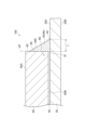
- FIG. 2 is a cross-sectional view of the joint body taken along the thickness direction of the metal plates.
- 1 is an example of a cross-sectional photograph (SEM photograph) of a joint taken with a scanning electron microscope (SEM) along the thickness direction of the metal plates.
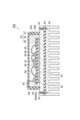
- FIG. FIG. 2 is a cross-sectional view of a power module.
- FIG. 2 is a diagram showing a support plate and a temporary fastening material attached thereto.
- FIG. 13 is a diagram showing a support plate and a metal plate temporarily fixed thereto.
- FIG. 13 is a diagram showing a state in which a coating layer formed on a ceramic plate and a support plate to which a metal plate is temporarily attached are laminated.
- FIG. FIG. 2 is a perspective view showing a portion of a first stack. 1 is a cross-sectional view taken along the thickness direction of a ceramic plate provided with a coating layer and a metal plate bonded to the coating layer. 3 is a cross-sectional view of a plurality of first laminates and a second laminate formed by stacking the first laminates.
- FIG. FIG. FIG. 4 is a cross-sectional view showing a state in which the second laminate is pressed by a pressing device.
- FIG. 4 is a cross-sectional view showing a state when a second stack is introduced into a heating device.
- 11 is a cross-sectional view showing a state in which a support plate is removed from the collective substrate.
- a numerical range that combines a numerical range having only an upper limit and a numerical range having only a lower limit is also included in this disclosure.
- a numerical range in which the upper limit or lower limit of each numerical range is replaced with the numerical value of any of the examples is also included in this disclosure.
- the joint includes a ceramic plate, a metal plate, and a joint portion that joins the main surface of the ceramic plate and the main surface of the metal plate and contains a brazing material component.
- the joint may be, for example, a circuit board.
- the metal plate may form an electric circuit or may be a heat sink.
- the number of metal plates joined to one main surface of a ceramic plate may be one or more.
- the metal plate may be joined to only one main surface of the ceramic plate, or to both main surfaces.
- the material of the ceramic plate is not particularly limited, and may be, for example, a nitride sintered body, a carbide sintered body, or an oxide sintered body.
- the ceramic plate is in a plate shape.
- the thickness of the ceramic plate may be, for example, 0.2 to 2 mm, or 0.25 to 1.5 mm.
- the metal plate may be, for example, a copper plate.
- the side of the metal plate is formed by a cut surface.
- Such a metal plate is obtained, for example, by punching. Therefore, the metal plate may have sagging (sagging surface) and burrs (burr surface).
- the metal plate may be joined to the ceramic plate via a joint so that the burrs are located closer to the ceramic plate than the sagging. This makes it difficult for voids to occur at the joint at the end of the metal plate, and the end of the metal plate can be firmly fixed to the ceramic plate.
- the shape of the metal plate is not particularly limited, and may be a prismatic or quadrangular prism shape. At least some of the corners of the metal plate may be chamfered.
- the thickness of the metal plate may be, for example, 0.1 to 2.0 mm, or 0.2 to 1.5 mm.
- the metal plate may have a plating film on its surface.
- the bonding layer is a layer that bonds the ceramic plate and the metal plate, and contains a brazing material component. For this reason, it is sometimes called a brazing material layer.
- the bonding layer may contain, for example, silver derived from the brazing material, or silver and copper.
- the bonding layer may further contain one or more metals selected from the group consisting of tin and active metals derived from the brazing material. In the bonding layer, the two or more metals may be an alloy.
- the active metal may contain one or more metals selected from the group consisting of titanium, hafnium, zirconium, and niobium.
- the silver and copper contained in the bonding layer may be contained as an alloy such as an Ag-Cu eutectic alloy.
- the silver content in the bonding layer may be 45 to 95 mass% or 50 to 95 mass% in terms of Ag.
- the total content of silver and copper in the bonding layer may be 65 to 100 mass%, 70 to 99 mass%, or 90 to 98 mass% in terms of Ag and Cu, respectively. This makes it possible to sufficiently reduce residual stress in the bonding layer while improving the density of the bonding layer.
- the content of the active metal in the bonding layer may be 0.5 to 8 parts by mass per 100 parts by mass of the total of Ag and Cu. By making the content of the active metal 0.5 parts by mass or more, it is possible to improve the bond between the ceramic plate and the bonding layer. On the other hand, by making the content of the active metal 8 parts by mass or less, it is possible to suppress the formation of a brittle alloy layer at the bonding interface.
- the metals contained in the bonding layer may be contained as nitrides, oxides, carbides, or hydrides.
- the bonding layer may contain titanium nitride and/or titanium hydride (TiH 2 ). This allows the bonding strength between the ceramic plate and the metal plate to be sufficiently high.
- TiH 2 titanium nitride and/or titanium hydride
- the content of TiH 2 relative to a total of 100 parts by mass of Ag and Cu may be, for example, 1 to 8 parts by mass.
- FIG. 1 shows a part of a cross section of the joint along the thickness direction (stacking direction) of the metal plates.
- the joint 40 has a covering portion 42 that covers at least a part of the side surface 62 of the metal plate 60 and a part of the main surface 20A of the ceramic plate 20.
- the covering portion 42 has a skirt portion 44 that expands away from the side surface 62 of the metal plate 60 as it approaches the main surface 20A of the ceramic plate 20 from the main surface 60A of the metal plate 60.
- the inclined surface 44S that defines the outline of the skirt portion 44 extends from the side surface 62 of the metal plate 60 to the main surface 20A of the ceramic plate 20.
- the covering portion 42 may cover the entire side surface 62 of the metal plate 60.
- the covering portion 42 may not be entirely composed of the skirt portion 44.
- the covering portion 42 may have a portion that covers the metal plate 60 along the side surface 62 at the upper portion of the side surface 62 of the metal plate 60, and a skirt portion 44 that covers the lower portion or lower portion of the side surface 62 below the center.
- the average protrusion distance L of the covering portion 42 may be 0.1 mm or more, 0.15 mm or more, or 0.2 mm or more. By increasing the average protrusion distance L, the bonding strength between the metal plate 60 and the ceramic plate 20 can be sufficiently increased.
- the average value of the overhang distance L may be 0.6 mm or less, 0.5 mm or less, less than 0.5 mm, or 0.4 mm or less. By preventing the average value of the overhang distance L from becoming excessively large, it is possible to maintain sufficiently good insulation when the joined body 100 is used as a circuit board. In addition, it is possible to miniaturize the joined body 100 by making the ceramic plate 20 smaller.
- An example of the numerical range of the average value of the overhang distance L is 0.1 to 0.6 mm. This allows the above-mentioned characteristics to be achieved in a well-balanced manner.
- the average value of the protrusion distance L can be adjusted by the amount of brazing material applied when joining the ceramic plate 20 and the metal plate 60 and the pressure applied during joining, etc.
- the standard deviation of the protrusion distance L is less than 0.1 mm, and may be 0.09 mm or less, 0.08 mm or less, 0.07 mm or less, or 0.05 mm or less. In this way, by reducing the standard deviation of the protrusion distance L, it is possible to reduce the variation in the protrusion distance L of the covering portion 42 depending on the position. With such a joint 100, the entire end portion 65 of the metal plate 60 can be evenly joined to the ceramic plate by the joint 40. Therefore, the joint 100 has excellent joining reliability.
- the standard deviation of the overhang distance L may be, for example, 0.01 mm or more, or 0.02 mm or more. This allows the joint 100 to be manufactured efficiently and reduces manufacturing costs.
- An example of the range of the standard deviation of the overhang distance L is 0.01 mm or more and less than 0.1 mm. Such a joint 100 can be manufactured at low cost and has excellent connection reliability.
- the standard deviation of the overhang distance L can be adjusted by the positioning accuracy when joining the ceramic plate 20 and the metal plate 60. For example, the standard deviation of the overhang distance L can be reduced by increasing the positioning accuracy.
- the protruding distance L of the covering portion 42 can be measured as follows. A photograph of a cross section along the thickness direction of the metal plate 60 as shown in Figure 1 is taken using a scanning electron microscope (SEM). The magnification may be, for example, 50 to 200 times. In this photograph, an imaginary perpendicular line VP is drawn from the cut surface 63 of the metal plate 60 toward the main surface 20A of the ceramic plate 20. The intersection point IP between the imaginary perpendicular line VP and the main surface 20A of the ceramic plate 20 is found. Starting from the intersection point IP, the length of the covering portion 42 is measured along the main surface 20A of the ceramic plate 20. This length is the protruding distance L of the covering portion 42. The protruding distance L of the covering portion 42 may be found using the SEM photograph and a ruler, or may be found using image analysis software.
- SEM scanning electron microscope
- Photographs of 20 cross sections selected at random are taken, and the protruding distance L of the covering portion 42 at each cross section is measured.
- the arithmetic mean of the 20 measured values is the average protruding distance L.
- Figure 2 is an example of a cross-sectional photograph (SEM photograph) of a joint along the thickness direction (stacking direction) of the metal plates.
- the side 62 of the metal plate 60 in the portion close to the ceramic plate 20, may contain reaction products between the brazing material and the components contained in the metal plate 60 that are generated during the manufacture of the joint 100.
- an imaginary perpendicular line VP is drawn based on the cut surface 63 appearing at the top of the side surface 62 of the metal plate 60, the protrusion distance L can be measured with high reproducibility. If the cut surface 63 is not perpendicular to the main surface 20A of the ceramic plate 20, the imaginary perpendicular line VP can be drawn based on the outermost protruding part of the cut surface 63.
- a metal plate 60 (first metal plate) is joined to one main surface 20A of the ceramic plate 20 by a joint 40 (first joint).
- a second metal plate may be joined to the other main surface 20B of the ceramic plate 20 by a second joint.
- the size and shape of the first metal plate and the second metal plate may be the same or different.
- the second joint may also have a covering portion similar to that of the first joint.
- the number of first metal plates 60 (second metal plates) joined to the main surface 20A (main surface 20B) is not limited to one, and may be multiple.
- the size and shape of the multiple first metal plates 60 (second metal plates) may be the same or different.
- All of the multiple first metal plates may have the same shape as the covering portion 42 of the joint 40, or may have different shapes.
- the standard deviation of the protrusion distance L of the joint where at least one of the metal plates is joined should be less than 0.1 mm.
- the assembly substrate includes a ceramic plate (first ceramic plate) for multiple pieces, a plurality of metal plates having side surfaces formed by cut surfaces, and a plurality of joints that join one main surface of the ceramic plate to each main surface of the plurality of metal plates and contain a brazing material component.
- Each of the plurality of joints may have a coating that covers at least a portion of the side surface of the metal plate and a portion of the main surface of the ceramic plate.
- the standard deviation of the protruding distance L of the coating measured along the main surface of the ceramic plate from the intersection of the main surface of the ceramic plate and a virtual perpendicular line from the cut surface of the first metal plate to the main surface of the ceramic plate is less than 0.1 mm.
- the joint that joins the first metal plate and the ceramic plate may have a shape similar to that of the joint 40 having the coating 42 described above.
- FIG. 3 is a perspective view showing an example of an aggregate substrate.
- the aggregate substrate 200 comprises a ceramic plate 21 and a plurality of metal plates 60 joined to each of the main surface 21A and the main surface 21B of the ceramic plate 21.
- the ceramic plate 21 is divided into a plurality of sections by division lines SL1, SL2 formed on the main surface 21A.
- the main surface 21A is provided with a plurality of division lines SL1 extending along a first direction and arranged at equal intervals, and a plurality of division lines SL2 extending along a second direction perpendicular to the first direction and arranged at equal intervals.
- the division lines SL1 and SL2 are perpendicular to each other.
- the demarcation lines SL1, SL2 may be, for example, a number of depressions arranged in a straight line, or may have linear grooves. Specifically, they may be scribe lines formed with laser light. Examples of laser sources include carbon dioxide lasers and YAG lasers. Scribe lines can be formed by intermittently irradiating laser light from such laser sources. Note that the demarcation lines SL1, SL2 do not have to be arranged at equal intervals, and are not limited to being perpendicular. Furthermore, they may be curved rather than straight, or bent.
- the ceramic plate 21 has a plurality of partition regions DR defined by partition lines SL1 and SL2.
- a metal plate 60 is provided in each of the plurality of partition regions DR.
- the plurality of metal plates 60 are independent of each other.
- Each of the multiple metal plates 60 on the main surface 21A of the ceramic plate 21 is joined to the ceramic plate 21 by a joint 40.
- the joint 40 has a covering portion 42 that covers a part of the side surface 62 of the metal plate 60 and a part of the main surface 21A of the ceramic plate 21.
- Each of the covering portions 42 has a skirt portion 44, similar to the covering portion 42 shown in FIG. 1.
- each of the joining portions 40 that join the multiple metal plates 60 and the ceramic plate 21 has a skirt-shaped covering portion 42.
- the average value and standard deviation of the protruding distance L of each covering portion 42 may be the same as the numerical range described for the joined body 100.
- Each of the multiple metal plates 60 on the main surface 21B of the ceramic plate 21 may also be joined to the ceramic plate 21 by a joint having a shape similar to that of the joint 40 that joins the metal plates 60.
- This joint may have a covering portion similar to the covering portion 42 that covers a portion of the side of the metal plate 60 and a portion of the main surface 21B of the ceramic plate 21.
- the average value and standard deviation of the protruding distance L of this covering portion may be the same as the numerical range described above. This can improve the joining reliability between the metal plates 60 on the main surface 21B of the ceramic plate 21 and the ceramic plate 21.
- the joint 100 may be mounted in a power module as a circuit board.
- the metal plate 60 may function as a circuit board having a function of transmitting electrical signals, or as a heat sink having a function of transmitting heat.
- the metal plate 60 may also have both a function of transmitting heat and a function of transmitting electrical signals.
- the joint 100 has excellent bonding reliability between the metal plate 60 and the ceramic plate 20. This results in excellent connection reliability with external circuits such as semiconductor elements. Therefore, it is suitable as a component to be mounted in a power module that requires high reliability.
- the power module includes a joint (circuit board) and a semiconductor element electrically connected to the metal plate of the joint.
- the circuit board may be the joint 100 described above or a modified version thereof.
- the description of the joint 100 and its modified versions applies to the power module of this embodiment.
- Such a power module has excellent reliability.
- the joint and the semiconductor element may be sealed with resin.
- FIG. 4 is a cross-sectional view showing an example of a power module.
- the power module 300 includes a base plate 90 and a joint 101 that is joined to one side of the base plate 90 via solder 82.
- a metal plate 61 on one side of the joint 101 is joined to the base plate 90 via the solder 82.
- a semiconductor element 80 is attached to the metal plate 60 on the other side of the joint 101 via solder 81.
- the semiconductor element 80 is connected to a predetermined location of the metal plate 60 with a metal wire 84 such as an aluminum wire. In this way, the semiconductor element 80 and the metal plate 60 are electrically connected.
- a metal wire 84 such as an aluminum wire.
- the semiconductor element 80 and the metal plate 60 are electrically connected.
- one of the metal plates, metal plate 60a is connected to an electrode 83 that penetrates the housing 86 via solder 85.
- a housing 86 is disposed on one of the main surfaces of the base plate 90, and is integrated with the main surface to house the joint 101.
- the housing space formed by the one of the main surfaces of the base plate 90 and the housing 86 is filled with resin 95.
- the resin 95 seals the joint 101 and the semiconductor element 80.
- the resin may be, for example, a thermosetting resin or a photocurable resin.
- a cooling fin 92 which serves as a heat dissipation member, is joined to the other main surface of the base plate 90 via grease 94. Screws 93 are attached to the ends of the base plate 90 to secure the cooling fin 92 to the base plate 90.
- the base plate 90 and the cooling fin 92 may be made of aluminum. The base plate 90 and the cooling fin 92 function well as heat dissipation parts due to their high thermal conductivity.
- the metal plate 60 and the metal plate 61 are electrically insulated by the ceramic plate 20.
- the metal plate 60 (60a) may form an electrical circuit.
- the metal plate 60 and the metal plate 61 are respectively joined to the main surface 20A and the main surface 20B of the ceramic plate 20 by a joint (not shown) containing a brazing material component.
- the joint has a coating portion 42 as shown in Figures 1 and 2.
- the average value and standard deviation of the protruding distance L of the coating portion 42 are as described above.
- the metal plate 60 (metal plate 61) is joined to the ceramic plate 20 by the joint having such a coating portion 42. For this reason, the power module 300 has excellent reliability.
- the manufacturing method of the bonded body includes a punching process in which a metal substrate is punched to obtain a plurality of metal plates 60, a temporary fixing process in which the plurality of metal plates 60 are temporarily fixed to each of a pair of support plates using a first positioning jig, a coating process in which a brazing material is applied to the main surface 21A and the main surface 21B of a ceramic plate 21 for multiple pieces and dried to provide a plurality of coating layers on each of the main surface 21A and the main surface 21B, a lamination process in which the ceramic plate 21 is sandwiched between the pair of support plates using a second positioning jig so that the plurality of coating layers and the plurality of metal plates 60 face each other to produce a laminate, a bonding process in which the laminate is heated to bond the metal plate 60 and the ceramic plate 21, and a finishing process in which the ceramic plate 21 to which the metal plate 60 is bonded is divided to obtain a plurality of bonded bodies 100.
- the metal base material is punched out using, for example, a die. This results in a metal plate 60 whose side surfaces are cut surfaces. If the metal plate 60 has a rectangular prism shape, all four side surfaces may be cut surfaces.
- the metal plate 60 may have a sag on one main surface 60A and a burr on the other main surface 60B.
- the metal plate 60 is fixed to a predetermined position A1 on the support plate TP by a temporary fixing material 11 shown in FIG. 5.
- the support plate TP may be, for example, a carbon plate.
- the temporary fixing material 11 may disappear when heated in the joining process.
- the predetermined position A1 on the support plate TP is a position corresponding to the intended joining position A2 (see FIG. 9) of the metal plate 60 fixed on the ceramic plate 21. Specifically, it is a position where the metal plate 60 is placed at the intended joining position A2 on the ceramic plate 21 when the support plate TP is placed in an appropriate position on the ceramic plate 21.
- a single support plate TP is divided into a plurality of regions for the purpose of forming a plurality of joints.
- a temporary fixing material 11 for temporarily fixing the metal plate 60 is provided in each of the plurality of regions.
- a sheet-type adhesive can be used.
- the sheet-type adhesive is an adhesive tape that can bond the metal plate 60 to the support plate TP at room temperature.
- the adhesive tape can be bonded on both sides, and includes an adhesive layer made of an organic component and a release film that covers both sides of the adhesive layer.
- the release film is a member that protects both sides of the adhesive layer and is peeled off when used.
- the release film may be, for example, a transparent PET film.
- One side of the adhesive layer of the temporary fixing material 11 may be adhered to a predetermined position A1 of the support plate TP. Then, as shown in FIG. 6, the metal plate 60 is adhered to the other side of the adhesive layer of the temporary fixing material 11.
- the adhesive component forming the adhesive layer can be a material capable of bonding the support plate TP and the metal plate 60.
- the adhesive component can be, for example, an acrylic adhesive, a urethane adhesive, or a rubber adhesive. These adhesives are composed of organic components. Therefore, they are decomposed during heating in the bonding process. By adjusting the amount used, it is possible to adjust the amount so that no residue remains in the bonded body 100.
- An acrylic adhesive is an adhesive made of acrylic polymer.
- a urethane adhesive is an adhesive made of polyurethane (a condensation polymerization product of a compound with an isocyanate group and a compound with a hydroxyl group).
- a rubber adhesive is an adhesive made of natural or synthetic rubber. Examples of synthetic rubber include acrylic rubber and styrene butadiene rubber.
- the temporary fixing material 11 may be an adhesive tape that does not have a base layer that supports the adhesive layer.
- the temporary fixing material 11 may be a spray-type adhesive.
- a spray-type adhesive is a liquid adhesive that is capable of adhering the metal plate 60 to the support plate TP at room temperature and is made of organic components. This adhesive is intended to be used by spraying. For example, the adhesive can be sprayed onto a predetermined position A1 of the support plate TP, and the metal plate 60 can be adhered and fixed to the support plate TP via the adhesive as shown in FIG. 6.
- the spray-type adhesive may be a solvent-based adhesive, a rubber-based adhesive, or a synthetic resin-based adhesive.
- the adhesive component is an organic solvent, and for example, hexane, isohexane, toluene, acetone, butane, etc. can be used.
- the adhesive component may be natural rubber or synthetic rubber.
- acrylic rubber, styrene butadiene rubber, etc. can be used as the synthetic rubber.
- the adhesive component is a synthetic resin, and acrylic polymer, etc. can be used.
- the spray-type adhesive is placed at a predetermined position A1 on the support plate TP by an injector or the like.
- the injector has, for example, a container and a nozzle part that sprays the adhesive in the container.
- the container contains liquid adhesive containing a tackifying component and a propellant that sprays the adhesive.
- the propellant for example, dimethyl ether or LPG can be used.
- the adhesive in the container is sprayed or stopped from inside the container by operating a lever or the like attached to the nozzle part.
- FIG. 7 is a plan view showing the metal plate 60 being temporarily fixed with the temporary fixing material 11 while aligning the metal plate 60 to the predetermined position A1 using the lattice jig 3 installed on the support plate TP.
- FIG. 8 is a cross-sectional view taken along line VIII-VIII in FIG. 7.
- the lattice jig 3 may be removed from the support plate TP before being introduced into the heating furnace 8 (see FIG. 15) for the joining process. In this way, the material of the lattice jig 3 can be selected with a high degree of freedom.
- materials for the lattice jig 3 include polyethylene (e.g., high-density polyethylene), polypropylene, polyvinyl chloride, AS resin, acrylic resin, A2017 (duralumin), A5052 (aluminum alloy), etc. These materials have excellent workability.
- the lattice jig 3 has a frame portion 31, a number of alignment holes 32 formed in the frame portion 31, and a pair of handle portions 33 extending outward from the frame portion 31.
- the frame 31 has a rectangular shape that is substantially aligned with the outer periphery of the support plate TP, except for the handle portion 33.
- the lattice jig 3 can be set in an appropriate position relative to the support plate TP.
- a rectangular hole 32 is formed by the frame 31, the vertical wall portions 31a, and the horizontal wall portions 31b, or by the vertical wall portions 31a and the horizontal wall portions 31b.
- the multiple holes 32 are each positioned so that they are aligned with the outer edge Ed of a predetermined position A1 on the support plate TP.
- Each of the multiple holes 32 is larger than the metal plate 60 and has a rectangular shape that can accommodate the metal plate 60.
- the main surface of the metal plate 60 is generally rectangular, with four corners 64 where adjacent side surfaces 62 are bent and connected.
- the hole 32 is a rectangular hole into which the metal plate 60 fits, with four (multiple) corners 32a.
- the metal plate 60 is positioned at a predetermined position A1 when the corners 64 come into contact with a reference corner 32x among the multiple corners 32a of the hole 32.
- the lower right corner 32a is set as the reference corner 32x (see Figure 7).
- the hole portion 32 has a gap forming portion 32b.
- the gap forming portion 32b is a portion that forms a gap Sp between the metal plate 60 and the corner portion 64 of the metal plate 60 when the corner portion 64 of the metal plate 60 abuts against the reference corner portion 32x.
- a gap Sp is formed between the left side of the metal plate 60 and the alignment hole portion 32.
- the portion of the hole portion 32 that forms this gap Sp is the gap forming portion 32b.
- the lattice jig 3 is placed at an appropriate position on the support plate TP.
- the temporary fixing material 11 is placed in the hole portion 32 of the lattice jig 3.
- the metal plate 60 is inserted into the hole portion 32. At this time, the metal plate 60 is aligned to the predetermined position A1 using the lattice jig 3, and the metal plate 60 is fixed to the support plate TP by the temporary fixing material 11.
- a coating process is performed in which a coating layer 12 containing a brazing material is provided on the main surface 21A of the ceramic plate 21.
- Partition lines SL1, SL2 are formed on the main surface 21A of the ceramic plate 21.
- the parting lines SL1, SL2 may be scribe lines formed by irradiating a laser beam, for example. Examples of laser beams include a carbon dioxide laser and a YAG laser. Such parting lines SL1, SL2 can be used as cutting lines when dividing the assembly substrate in a later process.
- the brazing filler metal may contain Ag in the form of a metal element or a metal compound (alloy), and may contain, in addition to Ag, one or more metals selected from the group consisting of Cu, Sn, and active metals. The two or more metals may be alloyed.
- the active metal may contain one or more metals selected from the group consisting of Ti, Hf, Zr, and Nb.
- the brazing filler metal may contain 80 parts by mass or more of Ag per 100 parts by mass of Ag and Cu in total, 90 parts by mass or more, or 95 parts by mass or more.
- the creeping up of the brazing filler metal can be suppressed.
- Ag and Cu have a eutectic point near a mass ratio of 72:28. Therefore, the molten brazing filler metal reacts smoothly with the Cu contained in the metal plate to form a eutectic alloy. Therefore, the contact area between the bonding layer and the ceramic plate and the metal plate can be sufficiently and smoothly increased.
- the brazing material does not need to contain Cu.
- the content of the active metal in the brazing filler metal may be 0.5 to 8 parts by mass per 100 parts by mass of the total of Ag and Cu. By making the content of the active metal 0.5 parts by mass or more, it is possible to improve the bond between the ceramic plate and the brazing filler metal. On the other hand, by making the content of the active metal 8 parts by mass or less, it is possible to suppress the formation of a brittle alloy layer at the bonded interface.
- the active metal contained in the brazing material may be contained as a nitride, oxide, carbide, or hydride.
- the brazing material may contain titanium nitride and/or titanium hydride (TiH 2 ). This allows the bonding strength between the ceramic plate and the metal plate to be sufficiently high.
- TiH 2 titanium nitride and/or titanium hydride
- the content of TiH 2 relative to 100 parts by mass of the total of Ag and Cu may be, for example, 1 to 8 parts by mass.
- the brazing filler metal may contain, in addition to the metal or metal compound described above, an organic solvent, a binder, etc.
- the viscosity of the brazing filler metal may be, for example, 5 to 20 Pa ⁇ s.
- the organic solvent content in the brazing filler metal may be, for example, 5 to 25 mass %, and the binder content may be, for example, 2 to 15 mass %.
- a brazing material is applied to one of the main surfaces 21A of the ceramic plate 21 at the intended joining position A2 of the metal plate 60 to form a coating layer 12.
- the application method may be a roll coater method, a screen printing method, a transfer method, or the like.
- the intended joining position A2 corresponds to a predetermined position A1 of the support plate TP.
- the support plate TP is laminated on the ceramic plate 21 so that the metal plate 60 faces the main surface 21A of the ceramic plate 21. At this time, the metal plate 60 faces the intended joining position A2 of the ceramic plate 21.
- the solder material is applied to the intended joining position A2 of the metal plate 60 to form a coating layer 12.
- the application method is as described above.
- This intended joining position A2 corresponds to a predetermined position A1 of another support plate TP.
- This other support plate TP is laminated on the ceramic plate 21 so that the metal plate 60 faces the main surface 21B of the ceramic plate 21. At this time, the metal plate 60 faces the ceramic plate 21 at the intended joining position A2. In this way, a first laminate Xa as shown in FIG. 10 is formed.
- FIG. 11 shows a part of a cross section of a ceramic plate 21 provided with a coating layer 12 when cut along the thickness direction.
- the coating layer 12 is thicker at the ends surrounding the center than at the center. That is, the coating layer 12 has a thin coating portion 12B in the center and a thick coating portion 12A at the end (periphery).
- the brazing material is sufficiently filled between the end 65 of the metal plate 60 and the ceramic plate 21. Therefore, it is possible to sufficiently prevent the bonding between the metal plate 60 and the ceramic plate 21 from becoming insufficient.
- the other coating layers 12 may have a similar shape.
- the width of the coating layer 12 in FIG. 11 is the same as the width of the metal plate 60, but is not limited to this.
- the coating layer 12 may have a protruding portion that extends outward beyond the side surface 62 of the metal plate 60 along the main surface 21A of the ceramic plate 21. In this way, if the coating layer 12 has a protruding portion at the end, the covering portion 42 (skirt portion 44) can be made sufficiently large to further improve the joining reliability.
- the protruding distance L shown in FIG. 1 can be increased.
- the protruding distance L shown in FIG. 1 can be shortened.
- the ceramic plate 21 on which the coating layer 12 is formed and a pair of support plates TP to which the metal plate 60 is temporarily attached are aligned using an enclosing jig 5 and laminated to obtain the first laminate Xa of Figure 10.
- a similar procedure is repeated to obtain a plurality of first laminates Xa, which are then stacked.
- a second laminate XA is obtained in which a plurality of first laminates Xa are stacked.
- an enclosing jig 5 as shown in Figures 12 and 13 can be used.
- the enclosing jig 5 is a frame-shaped device that surrounds the rectangular periphery of the second laminate XA, and is an example of a second alignment jig that aligns the metal plate 60 and the ceramic plate 21 when stacking them.
- the enclosing jig 5 has an abutting wall portion 50 that is arranged along the periphery of the multiple first laminates Xa (FIG. 13).
- the abutting wall portion 50 has multiple partition walls 51, 52 that can be separated.
- the abutting wall portion 50 has a first partition wall portion 51 that is L-shaped in a plan view and a second partition wall portion 52 that is L-shaped in a plan view.
- the first laminate Xa forming the second laminate XA is rectangular in plan view, so the second laminate XA has four corners Xb.
- the first dividing wall 51 has a corner 51m bent to fit along the corner Xb of the second laminate XA.
- the second dividing wall 52 has a corner 52m bent to fit along the corner Xb of the second laminate XA.
- the first dividing wall 51 has a first alignment wall 51a and a second alignment wall 51b.
- the second dividing wall 52 has a third alignment wall 52a and a fourth alignment wall 52b.
- the first alignment wall 51a and the third alignment wall 52a are arranged opposite each other to sandwich the second laminate XA (first laminate Xa) accommodated in the storage space.
- the second alignment wall 51b and the fourth alignment wall 52b are arranged opposite each other to sandwich the second laminate XA (first laminate Xa) accommodated in the storage space.
- the enclosure jig 5 has an adjustment section 53 that connects the first partition wall section 51 and the second partition wall section 52.
- the adjustment section 53 is configured to be able to adjust the volume of the storage space enclosed by the first partition wall section 51 and the second partition wall section 52.
- the adjustment portion 53 includes, for example, a plurality of slits 53a (through holes) formed in the first dividing wall portion 51, a plurality of screw portions 54 inserted into the plurality of slits 53a, and a plurality of screw holes 55 formed in the second dividing wall portion 52.
- the second dividing wall portion 52 includes an end portion 52c that can abut against the first dividing wall portion 51, and the end portion 52c is provided with a screw hole 55 so as to overlap the slit 53a of the first dividing wall portion 51.
- the screw portion 54 includes a shaft portion 54a and a head portion 54b (locking portion). The shaft portion 54a is inserted into the slit 53a and is screwed into the screw hole 55.
- the head portion 54b is formed at one end of the shaft portion 54a and interferes with the periphery of the slit 53a of the first dividing wall portion 51.
- the periphery of the slit 53a is an engagement receiving portion 53b that receives the interference of the head portion 54b.
- the storage space shrinks when the screw part 54 is tightened, and expands when it is loosened.
- the enclosing jig 5 is placed on the base 71 of the pressure device 7.
- the multiple first laminates Xa are stacked in the storage space of the enclosing jig 5.
- the multiple first laminates Xa are stacked on the base 71 while being aligned by the enclosing jig 5.
- This results in a second laminate XA in which the multiple first laminates Xa are stacked in the storage space of the enclosing jig 5.
- the enclosing jig 5 may be placed around the second laminate XA to align them. This results in a second laminate XA in which the stacked positions of the multiple first laminates Xa are aligned with each other.
- the pressure device 7 includes a base 71 that supports the second laminate XA, multiple pillars 72 erected from the base 71, a cover plate 73 that abuts against the upper surface of the second laminate XA, multiple elastic bodies 74 arranged on the cover plate 73, a pressure plate 75 that is installed on the elastic bodies 74 and presses the elastic bodies 74, and a nut 76 (holding part) that holds the pressure plate 75 in a predetermined position.
- the column 72 has a screw groove formed therein.
- the column 72 penetrates the cover plate 73 and the pressure plate 75.
- the nut 76 is screwed onto the upper end of the column 72 and abuts against the upper surface of the pressure plate 75.
- An elastic body 74 is disposed between the cover plate 73 and the pressure plate 75. When the nut 76 is tightened, the pressure plate 75 is pressed down, compressing the elastic body 74. As a result, the second laminate XA is pressurized via the cover plate 73. This allows the metal plate 60 and the ceramic plate 21, which are aligned with high precision, to be sufficiently bonded via the coating layer 12.
- the average value of the protrusion distance L can be adjusted by changing the pressure applied here.
- the enclosing jig 5 is divided and separated from the second laminate XA while the second laminate XA is kept pressurized by the pressure device 7.
- the pressurized second laminate XA is stable, and even if the enclosing jig 5 is separated, there is no misalignment between the multiple first laminates Xa and between the ceramic plate 21 and the metal plate 60 that constitute the first laminate Xa. In this way, if the jig is removed before the joining process, there is no need to consider the heat resistance of the material that constitutes the enclosing jig 5. This allows for a high degree of freedom in material selection.
- Examples of materials that can be used to constitute the enclosing jig 5 include polyethylene (e.g., high-density polyethylene), polypropylene, polyvinyl chloride, AS resin, acrylic resin, A2017 (duralumin), and A5052 (aluminum alloy). These materials have the advantage of being highly processable.
- polyethylene e.g., high-density polyethylene
- polypropylene polypropylene
- polyvinyl chloride polyvinyl chloride
- AS resin acrylic resin
- A2017 diuralumin
- A5052 aluminum alloy
- the enclosing jig 5 may be introduced into the heating furnace 8 together with the second laminate XA while the enclosing jig 5 holds the second laminate XA without removing the enclosing jig 5.
- the enclosing jig 5 is made of a heat-resistant material.
- Such materials include carbon-based materials, boron nitride, iron-based S45C and SS400, stainless steel-based SUS304 and SUS303, and cemented carbide.
- Carbon-based materials include carbon graphite, C/C composites, glassy carbon, etc.
- Cemented carbide includes those containing tungsten carbide as the main component.
- the second laminate XA is introduced into the heating furnace 8 while being held under pressure by the pressure device 7.
- the heating furnace 8 is equipped with a heater 8a.
- the heater 8a heats the inside of the heating furnace 8 to a temperature at which the metal plate 60 and the ceramic plate 21 are bonded by the bonding portion.
- the metal plate 60 is a copper material
- the inside of the heating furnace 8 is heated to 600°C to 900°C.
- the metal plate 60 is an aluminum plate
- the inside of the heating furnace 8 is heated to 550°C to 650°C.
- the coating layer 12 containing the brazing material melts at this atmospheric temperature, and becomes the bonding portion 40 that bonds the metal plate 60 and the ceramic plate 21 by cooling and solidifying after heating.
- the temporary bonding material 11 that temporarily bonds the metal plate 60 to the support plate TP disappears by volatilization, etc.
- the first laminates Xa constituting the second laminate XA are each formed into the collective substrate 200 shown in FIG. 3 by a bonding process.
- the collective substrate 200 removed from the heating furnace 8 includes a ceramic plate 21 and a plurality of metal plates 60 bonded to the ceramic plate 21. Each of the metal plates 60 is bonded to the ceramic plate 21 by a bonding portion 40.
- the temporary fixing material 11 that fixed the metal plate 60 to the support plate TP disappears in the heating furnace 8. Therefore, as shown in FIG. 16, the support plate TP can be easily removed from the collective substrate 200.
- the collective substrate 200 is divided along the division lines SL1 and SL2. Then, a finishing process is performed as necessary to obtain a plurality of independent joined bodies 100.
- the assembly substrate 200 and the assembly 100 can be manufactured by mounting the metal plate obtained by punching onto a multi-piece ceramic plate.
- This mounting method allows the assembly substrate 200 and the assembly 100 to be obtained efficiently.
- the metal plate is temporarily fixed to the support plate while being aligned using a first alignment jig (lattice jig 3), and the support plate (metal plate) and the ceramic plate are laminated while being aligned using a second alignment jig (enclosure jig 5) to obtain the first laminate Xa (second laminate XA). This makes it possible to improve the alignment accuracy when joining the metal plate and the ceramic plate.
- this first laminate Xa (second laminate XA) is heated while being pressurized by the pressure device 7. Therefore, it is possible to obtain an assembly in which the coating layer and the metal plate are less likely to deviate from each other and the variation in the protrusion distance L is sufficiently small, and an assembly substrate from which such an assembly can be obtained.
- the aggregate substrate 200 is manufactured, but the present invention is not limited to this.
- an aggregate substrate different from the aggregate substrate 200 may be manufactured.
- the bonded body 100 may be manufactured without manufacturing the aggregate substrate 200.
- the first positioning jig is not limited to a lattice jig, and may be any jig that can improve the alignment accuracy when the metal plate is temporarily fixed.
- the second positioning jig is also not limited to an enclosure jig, and may be any jig that can improve the alignment accuracy when stacking the metal plate and the ceramic plate.
- the manufacturing method of the bonded body 100 and the aggregate substrate 200 is not limited to the above.
- the bonded body 100 and the aggregate substrate 200 may be manufactured by other means that aligns with high precision and applies sufficient pressure without using the first alignment jig, the second alignment jig, and the pressure device.
- the bonded body obtained by the above-mentioned manufacturing method may be used to manufacture a power module as shown in FIG. 4.
- the power module may be manufactured by mounting a semiconductor element on the bonded body using solder and wire bonding, etc., housing the bonded body and the semiconductor element in the housing space, and then sealing with resin.
- the present disclosure is in no way limited to the above-described embodiments.
- the structures and shapes of the metal plates and joints joined to each of the pair of main surfaces of the ceramic plate may be different from each other.
- the ceramic plate is not limited to one obtained by dividing an aggregate substrate.
- Example 1 [Preparation of aggregate substrate and bonded body]
- the sides of these copper plates were composed of cut surfaces.
- a silicon nitride ceramic plate (silicon nitride plate, thickness: 0.25 mm) and a brazing material were prepared.
- a brazing filler metal containing Ag, Sn, and TiH2 was prepared.
- the brazing filler metal contained 3 parts by mass of Sn and 3.5 parts by mass of TiH2 per 100 parts by mass of Ag. This brazing filler metal did not contain Cu.
- the main surface of the ceramic plate was divided into 24 separate regions by scribe lines.
- a brazing filler metal was applied to each region by screen printing to form a coating layer.
- the coating area of the coating layer was the same as the area of the main surface of the copper plate to be joined to the ceramic plate.
- the coating layer had a thin coating portion in the center and a thick coating portion at the end (around the thin coating portion) as shown in Figure 11.
- the thickness of the thick coating portion was 1.2 times the thickness of the thin coating portion.
- the width of the thick coating portion surrounding the thick coating portion was constant at 1.5 mm.
- the amount of brazing filler metal applied when forming the thick coating portion and the thin coating portion was as shown in Table 1.
- a carbon plate was prepared as a support plate.
- Adhesive tape was applied to 24 places on the carbon plate to create a temporary fixing material. These adhesive tapes were applied at positions corresponding to the positions of the coating layer on the main surface of the ceramic plate.
- 24 copper plates were temporarily fixed onto the carbon plate with the temporary fixing material while being positioned using a grid jig 3 as shown in Figure 7.
- the ceramic plate and carbon plate were laminated so that the copper plate and the coating layer faced each other while being aligned using an enclosure jig 5. At this time, the copper plates were laminated so that the burrs were on the coating layer side and the sagging was on the carbon plate side.
- the laminate was heated in a vacuum (1.0 ⁇ 10 ⁇ 3 Pa) at 790° C. for 1 hour while pressing it at 0.015 MPa using a pressing device as shown in FIG. 14.
- an aggregate substrate was obtained in which 24 copper plates were bonded to the main surface of the ceramic plate via a bonding layer containing a brazing material component.
- electroless plating was performed using a Ni—P plating solution (phosphorus concentration: 8 to 12 mass%) to form an aggregate substrate (multiple-piece circuit substrate) having a plating film on the copper plate.
- the aggregate substrate was divided along the scribe line to obtain 24 bonded bodies.
- Example 2 A bonded body was obtained in the same manner as in Example 1, except that a punched copper plate having a thickness of 1.2 mm was used.
- Example 3 A joint was obtained in the same manner as in Example 1, except that the coating amount when forming the thick coating portion at the end of the coating layer was as shown in Table 1.
- Example 4 A joint was obtained in the same manner as in Example 2, except that the coating amount when forming the thick coating portion at the end of the coating layer was set as shown in Table 1.
- Example 5 A bonded body was obtained in the same manner as in Example 1, except that a silicon nitride plate having a thickness of 1.0 mm was used.
- Example 6 A bonded assembly was obtained in the same manner as in Example 5, except that a punched copper plate having a thickness of 1.2 mm was used.
- Example 7 A joint was obtained in the same manner as in Example 5, except that the coating amount when forming the thick coating portion at the end of the coating layer was as shown in Table 1.
- Example 8 A joint was obtained in the same manner as in Example 6, except that the coating amount when forming the thick coating portion at the end of the coating layer was as shown in Table 1.
- Example 9 A bonded structure was obtained in the same manner as in Example 6, except that the coating layer had no thick or thin coating portion and had a constant thickness.
- Example 1 A joint was obtained in the same manner as in Example 3, except that no grid jig was used when temporarily fixing the 24 copper plates on the carbon plate with the temporary fixing material.
- Example 2 A bonded body was obtained in the same manner as in Example 2, except that no enclosing jig for alignment was used when laminating the ceramic plate and the carbon plate with the copper plate and the coating layer facing each other.
- ⁇ Ultrasonic Testing (SAT)> The bonding reliability of the ceramic plate and the copper plate of each example and each comparative example was evaluated by ultrasonic inspection. Specifically, the area ratio of the void between the ceramic plate and the copper plate was calculated using an ultrasonic inspection device (device name: Fine SAT V) manufactured by Hitachi Power Solutions Co., Ltd. Inspection of 24 circuit boards was performed using image analysis software (GIMP) to calculate the average value of the ratio of the area of the void to the area of the copper plate in a plan view. Based on the calculation results, evaluation was performed according to the following criteria. The evaluation results are shown in Tables 1, 2, and 3. A: The average void area ratio is 2% or less. B: The average void area ratio is more than 2% and less than 4%. C: The average void area ratio is more than 4% and less than 6%. D: The average void area ratio is more than 6%.
- the joints of Examples 1 to 8 which were produced using a temporary fixing material, a lattice jig, and an enclosure jig, and in which the ends of the brazing material coating layer were made thicker than the center, had a sufficiently small void area ratio.
- the joint of Example 9 which was produced using a temporary fixing material, a lattice jig, and an enclosure jig, also had a small void area ratio.
- Comparative Examples 1 and 2 which did not use either the positioning jig or the lattice jig, the variation in the protrusion distance L was large, with a standard deviation of 0.10 mm or more. This is thought to be due to low alignment accuracy between the copper plate and the coating layer, which caused the two to become misaligned.
- a bonded body with excellent bonding reliability and a manufacturing method thereof can be provided.
- An assembly substrate can be provided that enables efficient production of a bonded body with excellent bonding reliability.
- a power module with excellent reliability can be provided.
Landscapes
- Ceramic Products (AREA)
Priority Applications (1)
| Application Number | Priority Date | Filing Date | Title |
|---|---|---|---|
| JP2024521298A JP7545615B1 (ja) | 2022-11-25 | 2023-11-16 | 接合体及びその製造方法、集合基板、並びにパワーモジュール |
Applications Claiming Priority (2)
| Application Number | Priority Date | Filing Date | Title |
|---|---|---|---|
| JP2022-188495 | 2022-11-25 | ||
| JP2022188495 | 2022-11-25 |
Publications (1)
| Publication Number | Publication Date |
|---|---|
| WO2024111503A1 true WO2024111503A1 (ja) | 2024-05-30 |
Family
ID=91195657
Family Applications (1)
| Application Number | Title | Priority Date | Filing Date |
|---|---|---|---|
| PCT/JP2023/041299 Ceased WO2024111503A1 (ja) | 2022-11-25 | 2023-11-16 | 接合体及びその製造方法、集合基板、並びにパワーモジュール |
Country Status (2)
| Country | Link |
|---|---|
| JP (1) | JP7545615B1 (https=) |
| WO (1) | WO2024111503A1 (https=) |
Citations (5)
| Publication number | Priority date | Publication date | Assignee | Title |
|---|---|---|---|---|
| JP2004307307A (ja) * | 2003-04-10 | 2004-11-04 | Hitachi Metals Ltd | セラミックス回路基板とその製造方法 |
| JP2005268821A (ja) * | 2005-05-24 | 2005-09-29 | Hitachi Metals Ltd | セラミックス回路基板及びこれを用いたパワー半導体モジュール |
| JP2013125908A (ja) * | 2011-12-15 | 2013-06-24 | Mitsubishi Materials Corp | パワーモジュール用基板の製造方法および製造装置 |
| JP2018011020A (ja) * | 2016-07-15 | 2018-01-18 | 京セラ株式会社 | 複合基板および電子装置 |
| JP2022132865A (ja) * | 2021-03-01 | 2022-09-13 | 三菱マテリアル株式会社 | 絶縁回路基板の製造方法 |
Family Cites Families (3)
| Publication number | Priority date | Publication date | Assignee | Title |
|---|---|---|---|---|
| EP0935286A4 (en) * | 1997-05-26 | 2008-04-09 | Sumitomo Electric Industries | COPPER CIRCUIT CONNECTING SUBSTRATE AND ITS MANUFACTURE |
| JP2004342635A (ja) * | 2003-05-13 | 2004-12-02 | Hitachi Metals Ltd | セラミックス基板接合用金属板およびセラミックス回路基板 |
| WO2021149789A1 (ja) * | 2020-01-23 | 2021-07-29 | デンカ株式会社 | セラミックス-銅複合体、及びセラミックス-銅複合体の製造方法 |
-
2023
- 2023-11-16 JP JP2024521298A patent/JP7545615B1/ja active Active
- 2023-11-16 WO PCT/JP2023/041299 patent/WO2024111503A1/ja not_active Ceased
Patent Citations (5)
| Publication number | Priority date | Publication date | Assignee | Title |
|---|---|---|---|---|
| JP2004307307A (ja) * | 2003-04-10 | 2004-11-04 | Hitachi Metals Ltd | セラミックス回路基板とその製造方法 |
| JP2005268821A (ja) * | 2005-05-24 | 2005-09-29 | Hitachi Metals Ltd | セラミックス回路基板及びこれを用いたパワー半導体モジュール |
| JP2013125908A (ja) * | 2011-12-15 | 2013-06-24 | Mitsubishi Materials Corp | パワーモジュール用基板の製造方法および製造装置 |
| JP2018011020A (ja) * | 2016-07-15 | 2018-01-18 | 京セラ株式会社 | 複合基板および電子装置 |
| JP2022132865A (ja) * | 2021-03-01 | 2022-09-13 | 三菱マテリアル株式会社 | 絶縁回路基板の製造方法 |
Also Published As
| Publication number | Publication date |
|---|---|
| JP7545615B1 (ja) | 2024-09-04 |
| JPWO2024111503A1 (https=) | 2024-05-30 |
Similar Documents
| Publication | Publication Date | Title |
|---|---|---|
| US6924429B2 (en) | Electronic device and production method therefor | |
| JP5664679B2 (ja) | パワーモジュール用基板の製造方法 | |
| JP3512225B2 (ja) | 多層配線基板の製造方法 | |
| JP3452678B2 (ja) | 配線構成体の製造方法 | |
| US20180090414A1 (en) | Ceramic substrate manufacturing method and ceramic substrate manufactured thereby | |
| EP2654079A2 (en) | Heat dissipation device and method for manufacturing the same | |
| TW200926917A (en) | Method of dicing a circuit board sheet and package circuit board | |
| CN104347267A (zh) | 电子部件的制造方法以及基板型端子的制造方法 | |
| JP7545615B1 (ja) | 接合体及びその製造方法、集合基板、並びにパワーモジュール | |
| JP2012227362A (ja) | ヒートシンク付パワーモジュール用基板ユニットおよびその製造方法 | |
| US7685707B2 (en) | Method for manufacturing circuit forming substrate | |
| JP2013051389A (ja) | 回路基板、半導体パワーモジュール、製造方法 | |
| WO2024111507A1 (ja) | 接合体及びその製造方法、集合基板、並びにパワーモジュール | |
| JP7535198B2 (ja) | 回路基板及びその製造方法、並びにパワーモジュール | |
| WO2013018357A1 (ja) | 半導体パワーモジュール、半導体パワーモジュールの製造方法、回路基板 | |
| JP2025053936A (ja) | 回路基板及びその製造方法 | |
| JP2019207952A (ja) | 電子素子実装用基板、電子装置、および電子モジュール | |
| JP2011073194A (ja) | 金属−セラミックス接合基板およびその製造方法 | |
| JP2010212723A (ja) | 半導体装置の製造方法 | |
| WO2019198551A1 (ja) | セラミックス-金属接合体およびその製造方法、多数個取り用セラミックス-金属接合体およびその製造方法 | |
| WO2024176598A1 (ja) | 回路基板、及びパワーモジュール | |
| KR101758379B1 (ko) | 파워 모듈용 기판의 제조 방법, 파워 모듈용 기판, 히트싱크가 부착된 파워 모듈용 기판 및 파워 모듈 | |
| JPH02137392A (ja) | プリント配線板 | |
| WO2024176599A1 (ja) | 回路基板の製造方法、回路基板、及びパワーモジュール | |
| WO2023190253A1 (ja) | 回路基板及びその製造方法、並びにパワーモジュール |
Legal Events
| Date | Code | Title | Description |
|---|---|---|---|
| WWE | Wipo information: entry into national phase |
Ref document number: 2024521298 Country of ref document: JP |
|
| 121 | Ep: the epo has been informed by wipo that ep was designated in this application |
Ref document number: 23894512 Country of ref document: EP Kind code of ref document: A1 |
|
| NENP | Non-entry into the national phase |
Ref country code: DE |
|
| 122 | Ep: pct application non-entry in european phase |
Ref document number: 23894512 Country of ref document: EP Kind code of ref document: A1 |