WO2024084762A1 - プラズマ処理装置 - Google Patents
プラズマ処理装置 Download PDFInfo
- Publication number
- WO2024084762A1 WO2024084762A1 PCT/JP2023/026919 JP2023026919W WO2024084762A1 WO 2024084762 A1 WO2024084762 A1 WO 2024084762A1 JP 2023026919 W JP2023026919 W JP 2023026919W WO 2024084762 A1 WO2024084762 A1 WO 2024084762A1
- Authority
- WO
- WIPO (PCT)
- Prior art keywords
- microwave power
- microwave
- plasma processing
- circuit unit
- processing chamber
- Prior art date
- Legal status (The legal status is an assumption and is not a legal conclusion. Google has not performed a legal analysis and makes no representation as to the accuracy of the status listed.)
- Ceased
Links
Images




Classifications
-
- H—ELECTRICITY
- H01—ELECTRIC ELEMENTS
- H01J—ELECTRIC DISCHARGE TUBES OR DISCHARGE LAMPS
- H01J37/00—Discharge tubes with provision for introducing objects or material to be exposed to the discharge, e.g. for the purpose of examination or processing thereof
- H01J37/32—Gas-filled discharge tubes
- H01J37/32009—Arrangements for generation of plasma specially adapted for examination or treatment of objects, e.g. plasma sources
- H01J37/32192—Microwave generated discharge
- H01J37/32211—Means for coupling power to the plasma
- H01J37/32229—Waveguides
-
- H—ELECTRICITY
- H01—ELECTRIC ELEMENTS
- H01J—ELECTRIC DISCHARGE TUBES OR DISCHARGE LAMPS
- H01J37/00—Discharge tubes with provision for introducing objects or material to be exposed to the discharge, e.g. for the purpose of examination or processing thereof
- H01J37/32—Gas-filled discharge tubes
-
- H—ELECTRICITY
- H01—ELECTRIC ELEMENTS
- H01J—ELECTRIC DISCHARGE TUBES OR DISCHARGE LAMPS
- H01J37/00—Discharge tubes with provision for introducing objects or material to be exposed to the discharge, e.g. for the purpose of examination or processing thereof
- H01J37/32—Gas-filled discharge tubes
- H01J37/32009—Arrangements for generation of plasma specially adapted for examination or treatment of objects, e.g. plasma sources
- H01J37/32192—Microwave generated discharge
-
- H—ELECTRICITY
- H01—ELECTRIC ELEMENTS
- H01J—ELECTRIC DISCHARGE TUBES OR DISCHARGE LAMPS
- H01J37/00—Discharge tubes with provision for introducing objects or material to be exposed to the discharge, e.g. for the purpose of examination or processing thereof
- H01J37/32—Gas-filled discharge tubes
- H01J37/32009—Arrangements for generation of plasma specially adapted for examination or treatment of objects, e.g. plasma sources
- H01J37/32192—Microwave generated discharge
- H01J37/32211—Means for coupling power to the plasma
- H01J37/32247—Resonators
-
- H—ELECTRICITY
- H01—ELECTRIC ELEMENTS
- H01J—ELECTRIC DISCHARGE TUBES OR DISCHARGE LAMPS
- H01J37/00—Discharge tubes with provision for introducing objects or material to be exposed to the discharge, e.g. for the purpose of examination or processing thereof
- H01J37/32—Gas-filled discharge tubes
- H01J37/32009—Arrangements for generation of plasma specially adapted for examination or treatment of objects, e.g. plasma sources
- H01J37/32192—Microwave generated discharge
- H01J37/32311—Circuits specially adapted for controlling the microwave discharge
-
- H—ELECTRICITY
- H05—ELECTRIC TECHNIQUES NOT OTHERWISE PROVIDED FOR
- H05H—PLASMA TECHNIQUE; PRODUCTION OF ACCELERATED ELECTRICALLY-CHARGED PARTICLES OR OF NEUTRONS; PRODUCTION OR ACCELERATION OF NEUTRAL MOLECULAR OR ATOMIC BEAMS
- H05H1/00—Generating plasma; Handling plasma
- H05H1/24—Generating plasma
- H05H1/46—Generating plasma using applied electromagnetic fields, e.g. high frequency or microwave energy
-
- H—ELECTRICITY
- H01—ELECTRIC ELEMENTS
- H01J—ELECTRIC DISCHARGE TUBES OR DISCHARGE LAMPS
- H01J2237/00—Discharge tubes exposing object to beam, e.g. for analysis treatment, etching, imaging
- H01J2237/32—Processing objects by plasma generation
- H01J2237/33—Processing objects by plasma generation characterised by the type of processing
- H01J2237/334—Etching
-
- H—ELECTRICITY
- H01—ELECTRIC ELEMENTS
- H01J—ELECTRIC DISCHARGE TUBES OR DISCHARGE LAMPS
- H01J37/00—Discharge tubes with provision for introducing objects or material to be exposed to the discharge, e.g. for the purpose of examination or processing thereof
- H01J37/32—Gas-filled discharge tubes
- H01J37/32431—Constructional details of the reactor
- H01J37/3266—Magnetic control means
- H01J37/32669—Particular magnets or magnet arrangements for controlling the discharge
Definitions
- the present invention relates to a plasma processing apparatus that generates plasma using the interaction between microwaves and a static magnetic field, and in particular to an apparatus that configures a static magnetic field and a microwave three-dimensional circuit system so that the direction of the microwaves in the plasma processing chamber is approximately perpendicular to the direction of the static magnetic field, and the direction of the microwave electric field is approximately perpendicular to the direction of the static magnetic field, and that optimizes the microwave three-dimensional circuit system from the viewpoint of plasma density distribution in the processing chamber.
- Plasma processing equipment is used in the production of semiconductor integrated circuit elements.
- the miniaturization of elements has progressed to improve element performance and reduce costs.
- two-dimensional miniaturization of elements increased the number of elements that could be produced from a single substrate to be processed, reducing the manufacturing cost per element and improving performance through miniaturization effects such as shortening wiring length.
- the difficulty of two-dimensional miniaturization increases significantly, and measures such as the application of new materials and three-dimensional element structures are being taken.
- the in-plane uniformity of the plasma treatment on the substrate being processed is also important.
- disk-shaped silicon wafers with a diameter of 300 mm are often used as the substrate being processed.
- Many semiconductor integrated circuit elements are often created on these silicon wafers, but if the in-plane uniformity of the plasma treatment is poor, the number of good products that meet the specifications that can be obtained from a single silicon wafer may be reduced.
- the stability of the plasma treatment for each substrate being processed is also important. If the quality of the plasma treatment is not stable, for example if the quality changes over time, the proportion of good products may similarly decrease.
- ECR Electron Cyclotron Resonance
- UHR Upper Hybrid Resonance
- a static magnetic field is applied approximately parallel to the central axis of a roughly cylindrical processing chamber, and microwaves are input from the side. Furthermore, the electric field of the microwaves is approximately perpendicular to the central axis of the processing chamber. These measures excite X-waves in the plasma in the processing chamber, and UHR is utilized. Furthermore, an electrode for placing the substrate to be processed is provided on one side of the processing chamber that is approximately perpendicular to the static magnetic field, and an earth electrode (called the opposing earth) is provided on the other side. This allows the RF bias described below to be efficiently applied to the substrate to be processed. Compared to devices using ECR, resonance can be caused by a weak static magnetic field, which has the advantages of reducing power consumption by the electromagnets used to generate the static magnetic field, and allowing the electromagnets to be made smaller, increasing the freedom of placement.
- the opposing earth is held by multiple pillars, and microwaves are efficiently introduced into the processing chamber by a three-dimensional microwave circuit system that includes a structure for suppressing the reflection of microwaves caused by discontinuous parts such as these pillars.
- magnetrons are widely used as microwave oscillators, but recently oscillators using solid-state elements have also come into use.
- Oscillators using solid-state elements have the advantage that the oscillation frequency and output are more stable than magnetrons, and various types of modulation can be easily applied.
- rectangular waveguides, circular waveguides, coaxial lines, etc. are used to transmit microwave power.
- they are often used in combination with an isolator to protect the microwave oscillator and an automatic matching device to prevent impedance mismatch with the load.
- the quality of the plasma processing can be improved by applying RF bias power to the substrate being processed.
- RF bias power for example, in the case of plasma etching processing, an RF bias with a frequency of about 400 kHz to 13.56 MHz generates a DC bias voltage in the substrate being processed due to the mass difference between ions and electrons, and this DC bias voltage attracts ions in the plasma, improving the verticality of the processed shape and the processing speed, thereby improving the quality of the plasma processing.
- the above-mentioned matching box is used, but if the degree of mismatch with the load is too large, it may be difficult to ensure a wide matching range corresponding to this, and large standing waves may occur between the matching box and the load, which may cause problems such as abnormal discharge and power loss.
- Patent Document 1 It was found that when the embodiment disclosed in Patent Document 1 is applied, depending on the plasma generation conditions, the plasma may be excessively localized near the side wall of the processing chamber, resulting in low plasma density near the substrate being processed.
- the present invention provides a plasma processing apparatus that solves the problems of the conventional technology described above and makes it possible to further improve the uniformity of plasma within the processing chamber.
- the present invention provides a plasma processing apparatus including a sample chamber having a sample stage therein on which a substrate to be processed is placed, a magnetic field generating means for generating a magnetic field inside the sample chamber, a microwave power source for generating microwave power, a microwave power carrier section for carrying the microwave power generated by the microwave power source, and a microwave three-dimensional circuit section for supplying the microwave power carried by the microwave power carrier section to the inside of the processing chamber through a dielectric window.
- the microwave three-dimensional circuit section is configured to include a branch circuit section for branching the microwave power carried by the microwave power carrier section in a plurality of azimuth directions, a ring resonator disposed around the branch circuit section for resonating the microwave power branched in the plurality of azimuth directions by the branch circuit section, and a coaxial line section connected to the ring resonator for supplying the microwave power resonated by the ring resonator to the inside of the processing chamber through the dielectric window.
- 1 is a front cross-sectional view showing a schematic configuration of a microwave plasma etching apparatus according to a conventional technology.
- 1 is a front cross-sectional view showing a schematic configuration of a microwave plasma etching apparatus according to an embodiment of the present invention.
- 1 is a vertical cross-sectional view showing a microwave three-dimensional circuit of a microwave plasma etching apparatus according to an embodiment of the present invention.
- 1 is a plan view of a microwave three-dimensional circuit of a microwave plasma etching apparatus according to an embodiment of the present invention.
- 3 is a front cross-sectional view of a ring resonator showing an electric field distribution in the ring resonator of the microwave plasma etching apparatus according to the embodiment of the present invention.
- FIG. 4B is a cross-sectional view of the ring resonator taken along line MM in FIG. 4A, showing the electric field distribution of the ring resonator in the microwave plasma etching apparatus according to the embodiment of the present invention.
- the present invention relates to a plasma processing apparatus that has a roughly cylindrical plasma processing chamber and generates plasma by inputting microwave power from the side of the plasma processing chamber.
- the proportion of microwave power that travels in the radial direction of the microwaves is small, and the generated plasma may be excessively localized near the inner side wall, resulting in low plasma density near the central axis of the plasma processing chamber.
- This problem is solved by using a ring resonator that resonates in a mode with an azimuthal direction dependency m value of 1 to input microwaves into the processing chamber in order to suppress the azimuthal direction propagation of the microwaves and increase the radial propagation component, thereby realizing a plasma processing apparatus that makes it possible to further improve the uniformity of plasma within the plasma processing chamber.
- This prior art is a plasma processing apparatus 100 for performing etching processing.
- Microwaves with a frequency of 2.45 GHz generated by a microwave source 0101 are transmitted to a circular waveguide 0106 via an isolator and an automatic matching device 0102 (not shown), a rectangular waveguide 0103, and a circular-to-rectangle converter 0104, which also serves as a corner for changing the transmission direction by 90 degrees.
- a circular polarized wave generator 0105 is loaded inside the circular waveguide 0106.
- the circular polarized wave generator 0105 has the function of converting microwaves incident as linearly polarized waves into circularly polarized waves.
- microwaves By circularly polarizing the microwaves, it is possible to generate plasma that is uniform in the azimuth direction.
- the microwaves are then transmitted to a coaxial line 0110 via an expansion section 0107.
- the microwave electric field distribution is shown diagrammatically by arrows inside the coaxial line 0110.
- an opposing earth 0109 fixed to the outside via multiple supports 0108.
- a cylindrical microwave introduction window 0111 Below the opposing earth 0109, inside the coaxial line 0110, is a cylindrical microwave introduction window 0111.
- the material of the microwave introduction window should preferably have low microwave loss, be plasma resistant, and be unlikely to adversely affect the plasma processing, and quartz is used.
- a ring-shaped alignment member 0119 is disposed on the inner periphery of the expansion section 0107 where it contacts the ceiling wall and side wall.
- the area formed by the opposing earth 0109 and the microwave introduction window 0111 constitutes the plasma processing chamber 0112.
- a substrate electrode 0114 Inside the plasma processing chamber, there is a substrate electrode 0114 on which a 300 mm diameter substrate 0113 to be processed is placed.
- An RF power supply 0115 is connected to the substrate electrode 0114 via an automatic matching box 0117, allowing an RF bias to be applied to the substrate 0113 to be processed.
- the RF power supply 0115 used has an oscillation frequency of 400 kHz.
- a multi-stage solenoid coil 0116 equipped with a yoke is provided around these mechanisms, allowing a static magnetic field to be applied inside the plasma processing chamber 0112.
- the substrate 0113 to be processed is disk-shaped, and the device is accordingly basically axially symmetrical, sharing a common axis with the central axis of the substrate 0113 to be processed.
- the base electrode 0114, coaxial line 0110, opposing earth 0109, expansion section 0107, circular waveguide 0106, and solenoid coil 0116 are arranged coaxially with the central axis of the roughly cylindrical plasma processing chamber 0112.
- the plasma processing chamber 0112 is connected to a gas supply system and a vacuum exhaust system (not shown), allowing the supply and exhaust of a predetermined flow rate of processing gas while maintaining a predetermined pressure.
- the opposing earth 0109 needs to be fixed to the external structure, and also contains a temperature control mechanism for cooling, etc., and a gas supply mechanism from the opposing earth, and is fixed to the outside with multiple supports 0108. Flow paths for the refrigerant and gas are provided within the supports 0108. Furthermore, the opposing earth 0109 is electrically connected to the outside by the supports 0108, stabilizing the electric potential.
- microwaves propagate as plane waves in a boundaryless vacuum at the speed of light, and the wavelength in the direction of wave travel is the speed of light divided by the frequency.
- microwaves are reflected so as to satisfy the boundary condition that the electric field vector is perpendicular to the perfect conductor surface.
- the inner wall of the waveguide can be analyzed as a perfect conductor, and the electromagnetic field distribution is determined by the superposition of each wave as it repeatedly reflects off the inner wall to satisfy the boundary condition.
- the microwave electromagnetic field inside is determined by repeated reflections on the inner walls in the same manner as above.
- the direction of wave propagation can be evaluated by a wave vector, which, when considered in a cylindrical coordinate system (r, ⁇ , z), has components in the radial (r), azimuthal ( ⁇ ), and height (z) directions.
- the z component of the wave vector is zero, and the wave propagates in the radial and azimuthal directions but not in the height direction.
- FIG. 2 The configuration of the plasma processing apparatus 200 according to this embodiment, which is based on the results of this study, is shown in FIG. 2, and the partial detailed configuration will be explained using FIG. 3A to FIG. 4B.
- the difference between the configuration of the plasma processing apparatus 200 according to this embodiment shown in FIG. 2 and the plasma processing apparatus 100 of the prior art shown in FIG. 1 is the microwave three-dimensional circuit portion that is configured with a branch circuit 0202 that inputs microwave power to the plasma processing chamber 0112, a ring resonator 0201, a coaxial line 0110, and an opposing earth 0203 with a convex portion 0204 formed in the center.
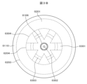
- the matching rod 0302, matching ridge 0303, and phase adjustment means 0304 that form the branch circuit 0202 will be explained using FIG. 3A and FIG. 3B.
- Other components with the same part numbers as those in FIG. 1 are the same as the configuration of the prior art plasma processing apparatus 100 explained in FIG. 1, and explanations of parts common to this embodiment will be omitted.
- the microwaves circularly polarized by the circular polarizer 0105 and transmitted through the circular waveguide 0106 are branched by a branch circuit 0202 formed on the upper surface 0204 of the convex portion of the opposing earth 0203 directly below the circular waveguide 0106, and excite a ring resonator 0201 formed around the side surface 0205 of the convex portion of the opposing earth 0203. Furthermore, a coaxial line 0110 is connected to the ring resonator 0201, and the microwaves are input into the plasma processing chamber 0112 through a microwave introduction window 0111.
- the branch circuit 0202 and its surroundings will be described in detail with reference to Figures 3A and 3B.
- Figure 3A is a side cross-sectional view
- Figure 3B is a plan view.
- the branch circuit 0202 has the role of transmitting microwaves transmitted from the circular waveguide 0106 to the ring resonator 0201, and is composed of a rectangular waveguide 0301 branched into six by phase adjustment means 0304, a matching rod (first matching section) 0302 that suppresses reflected waves at the branch point between the circular waveguide 0106 and the rectangular waveguide 0301, and a matching ridge (second matching section) 0303 that suppresses reflections from the connection surface with the ring resonator 0201, etc.
- the rectangular waveguide 0301 is arranged with six phase adjustment means 0304 branching out at equal intervals of 60 degrees in the azimuth direction to branch microwave power in six directions, but the number of branches may be an integer equal to or greater than 3.
- the rectangular waveguide 0301 is sized to operate in the TE 10 mode, which is the lowest order mode of a rectangular waveguide.
- the matching rod 0302 is cylindrical and arranged coaxially with the circular waveguide 0106. By optimizing its diameter and height, it is possible to suppress reflected waves at the connection surface between the circular waveguide 0106 and the multiple rectangular waveguides 0301. Similarly, the position, height, and width of the matching ridge 0303 can be adjusted to suppress reflected waves caused by discontinuous surfaces after the rectangular waveguide 0301.
- the microwave power incident from the circular waveguide 0106 can be efficiently transmitted to the inside of the processing chamber.
- the matching rod 0302 and matching ridge 0303 may be omitted.
- the coaxial line 0110 connected to the ring resonator 0201 has a microwave introduction window 0111 as described in FIG. 2 attached to its inner circumference, and the bottom surface of the coaxial line 0110 is closed, but in FIG. 3A, the microwave introduction window 0111 is omitted, and the bottom surface of the coaxial line 0110 is shown open.
- a desired electromagnetic field can be obtained by using a resonator that resonates with the desired electromagnetic field.
- Fig. 4A shows a longitudinal section
- Fig. 4B shows an M-M cross section of Fig. 4A.
- the TM110 mode can be considered as a mode in which a rectangular waveguide of one wavelength length operating in the lowest order TE10 mode is bent into a ring shape.
- the wave number vector which indicates the direction of wave travel, only has azimuth and radial components, and does not have a component parallel to the central axis.
- the resonance condition of the TM110 mode ring resonator does not depend on the dimension parallel to the central axis (H in FIG. 4A), but only on the inner radius (a in FIG. 4A) and the outer radius (b in FIG. 4A) of the ring. Since a circularly polarized wave is supplied to the circular waveguide, the electromagnetic field in the ring resonator 0201 shown in FIG. 4A and FIG. 4B rotates in time in the azimuth direction.
- Equation 1 The dimensions of the ring resonator can be found by solving this equation (Equation 1).
- there are no structures that are discontinuous in the azimuth direction on the path from the coaxial line to the plasma processing chamber, and the m 1 distribution within the ring resonator is maintained to excite the coaxial line.
Landscapes
- Physics & Mathematics (AREA)
- Engineering & Computer Science (AREA)
- Plasma & Fusion (AREA)
- Chemical & Material Sciences (AREA)
- Analytical Chemistry (AREA)
- Electromagnetism (AREA)
- Spectroscopy & Molecular Physics (AREA)
- Drying Of Semiconductors (AREA)
- Plasma Technology (AREA)
- ing And Chemical Polishing (AREA)
Priority Applications (4)
| Application Number | Priority Date | Filing Date | Title |
|---|---|---|---|
| CN202380013048.3A CN118235528A (zh) | 2022-10-19 | 2023-07-24 | 等离子处理装置 |
| US18/691,299 US12444575B2 (en) | 2022-10-19 | 2023-07-24 | Plasma processing apparatus |
| KR1020247002378A KR102820386B1 (ko) | 2022-10-19 | 2023-07-24 | 플라스마 처리 장치 |
| JP2024505020A JP7637315B2 (ja) | 2022-10-19 | 2023-07-24 | プラズマ処理装置 |
Applications Claiming Priority (2)
| Application Number | Priority Date | Filing Date | Title |
|---|---|---|---|
| JP2022167445 | 2022-10-19 | ||
| JP2022-167445 | 2022-10-19 |
Publications (1)
| Publication Number | Publication Date |
|---|---|
| WO2024084762A1 true WO2024084762A1 (ja) | 2024-04-25 |
Family
ID=90737465
Family Applications (1)
| Application Number | Title | Priority Date | Filing Date |
|---|---|---|---|
| PCT/JP2023/026919 Ceased WO2024084762A1 (ja) | 2022-10-19 | 2023-07-24 | プラズマ処理装置 |
Country Status (6)
| Country | Link |
|---|---|
| US (1) | US12444575B2 (https=) |
| JP (1) | JP7637315B2 (https=) |
| KR (1) | KR102820386B1 (https=) |
| CN (1) | CN118235528A (https=) |
| TW (1) | TWI899592B (https=) |
| WO (1) | WO2024084762A1 (https=) |
Cited By (2)
| Publication number | Priority date | Publication date | Assignee | Title |
|---|---|---|---|---|
| CN119835850A (zh) * | 2025-03-18 | 2025-04-15 | 深空探测实验室(天都实验室) | 一种磁膨胀腔结构高能离子束发生装置 |
| US12444575B2 (en) * | 2022-10-19 | 2025-10-14 | Hitachi High-Tech Corporation | Plasma processing apparatus |
Citations (2)
| Publication number | Priority date | Publication date | Assignee | Title |
|---|---|---|---|---|
| JP2012190899A (ja) * | 2011-03-09 | 2012-10-04 | Hitachi High-Technologies Corp | プラズマ処理装置 |
| JP7139528B2 (ja) * | 2020-04-27 | 2022-09-20 | 株式会社日立ハイテク | プラズマ処理装置 |
Family Cites Families (30)
| Publication number | Priority date | Publication date | Assignee | Title |
|---|---|---|---|---|
| JP3469987B2 (ja) | 1996-04-01 | 2003-11-25 | 株式会社日立製作所 | プラズマ処理装置 |
| US2716221A (en) | 1950-09-25 | 1955-08-23 | Philip J Allen | Rotatable dielectric slab phase-shifter for waveguide |
| JP2569019B2 (ja) * | 1986-10-20 | 1997-01-08 | 株式会社日立製作所 | エッチング方法及びその装置 |
| US5359177A (en) * | 1990-11-14 | 1994-10-25 | Mitsubishi Denki Kabushiki Kaisha | Microwave plasma apparatus for generating a uniform plasma |
| EP0502269A1 (en) | 1991-03-06 | 1992-09-09 | Hitachi, Ltd. | Method of and system for microwave plasma treatments |
| US5230740A (en) | 1991-12-17 | 1993-07-27 | Crystallume | Apparatus for controlling plasma size and position in plasma-activated chemical vapor deposition processes comprising rotating dielectric |
| DE4235914A1 (de) * | 1992-10-23 | 1994-04-28 | Juergen Prof Dr Engemann | Vorrichtung zur Erzeugung von Mikrowellenplasmen |
| KR970071945A (ko) | 1996-02-20 | 1997-11-07 | 가나이 쯔도무 | 플라즈마처리방법 및 장치 |
| US5874706A (en) * | 1996-09-26 | 1999-02-23 | Tokyo Electron Limited | Microwave plasma processing apparatus using a hybrid microwave having two different modes of oscillation or branched microwaves forming a concentric electric field |
| DE19802971C2 (de) * | 1998-01-27 | 1999-12-02 | Fraunhofer Ges Forschung | Plasmareaktor |
| US6652709B1 (en) | 1999-11-02 | 2003-11-25 | Canon Kabushiki Kaisha | Plasma processing apparatus having circular waveguide, and plasma processing method |
| JP4441038B2 (ja) | 2000-02-07 | 2010-03-31 | 東京エレクトロン株式会社 | マイクロ波プラズマ処理装置 |
| US6677549B2 (en) | 2000-07-24 | 2004-01-13 | Canon Kabushiki Kaisha | Plasma processing apparatus having permeable window covered with light shielding film |
| CN100573827C (zh) | 2001-09-27 | 2009-12-23 | 东京毅力科创株式会社 | 电磁场供给装置及等离子体处理装置 |
| JP2007035411A (ja) | 2005-07-26 | 2007-02-08 | Hitachi High-Technologies Corp | プラズマ処理装置 |
| JP2007035412A (ja) | 2005-07-26 | 2007-02-08 | Hitachi High-Technologies Corp | プラズマ処理装置 |
| EP2086285A1 (en) * | 2008-02-01 | 2009-08-05 | Anton Paar GmbH | Applicator and Apparatus for heating samples by microwave radiation |
| JP2010050046A (ja) | 2008-08-25 | 2010-03-04 | Hitachi High-Technologies Corp | プラズマ処理装置 |
| JP2012044035A (ja) | 2010-08-20 | 2012-03-01 | Hitachi High-Technologies Corp | 半導体製造装置 |
| JP2012049353A (ja) * | 2010-08-27 | 2012-03-08 | Hitachi High-Technologies Corp | プラズマ処理装置 |
| JP5690603B2 (ja) * | 2011-01-26 | 2015-03-25 | 株式会社日立ハイテクノロジーズ | プラズマ処理装置 |
| CN103262663B (zh) * | 2011-04-28 | 2016-12-14 | 住友理工株式会社 | 微波等离子体生成装置和采用该装置的磁控溅射成膜装置 |
| JP6442242B2 (ja) * | 2014-11-17 | 2018-12-19 | 株式会社日立ハイテクノロジーズ | プラズマ処理装置 |
| JP7001456B2 (ja) | 2017-12-19 | 2022-01-19 | 株式会社日立ハイテク | プラズマ処理装置 |
| JP7184254B2 (ja) * | 2018-12-06 | 2022-12-06 | 東京エレクトロン株式会社 | プラズマ処理装置及びプラズマ処理方法 |
| CN113454760B (zh) * | 2020-01-27 | 2024-03-22 | 株式会社日立高新技术 | 等离子处理装置 |
| WO2021220459A1 (ja) * | 2020-04-30 | 2021-11-04 | 株式会社日立ハイテク | プラズマ処理装置 |
| JP7302094B2 (ja) * | 2021-01-21 | 2023-07-03 | 株式会社日立ハイテク | プラズマ処理装置 |
| KR102808893B1 (ko) * | 2021-02-19 | 2025-05-19 | 주식회사 히타치하이테크 | 플라스마 처리 장치 |
| TWI899592B (zh) * | 2022-10-19 | 2025-10-01 | 日商日立全球先端科技股份有限公司 | 電漿處理裝置 |
-
2023
- 2023-07-17 TW TW112126559A patent/TWI899592B/zh active
- 2023-07-24 CN CN202380013048.3A patent/CN118235528A/zh active Pending
- 2023-07-24 KR KR1020247002378A patent/KR102820386B1/ko active Active
- 2023-07-24 US US18/691,299 patent/US12444575B2/en active Active
- 2023-07-24 WO PCT/JP2023/026919 patent/WO2024084762A1/ja not_active Ceased
- 2023-07-24 JP JP2024505020A patent/JP7637315B2/ja active Active
Patent Citations (2)
| Publication number | Priority date | Publication date | Assignee | Title |
|---|---|---|---|---|
| JP2012190899A (ja) * | 2011-03-09 | 2012-10-04 | Hitachi High-Technologies Corp | プラズマ処理装置 |
| JP7139528B2 (ja) * | 2020-04-27 | 2022-09-20 | 株式会社日立ハイテク | プラズマ処理装置 |
Cited By (3)
| Publication number | Priority date | Publication date | Assignee | Title |
|---|---|---|---|---|
| US12444575B2 (en) * | 2022-10-19 | 2025-10-14 | Hitachi High-Tech Corporation | Plasma processing apparatus |
| CN119835850A (zh) * | 2025-03-18 | 2025-04-15 | 深空探测实验室(天都实验室) | 一种磁膨胀腔结构高能离子束发生装置 |
| CN119835850B (zh) * | 2025-03-18 | 2025-05-13 | 深空探测实验室(天都实验室) | 一种磁膨胀腔结构高能离子束发生装置 |
Also Published As
| Publication number | Publication date |
|---|---|
| US20250246410A1 (en) | 2025-07-31 |
| TW202418344A (zh) | 2024-05-01 |
| KR102820386B1 (ko) | 2025-06-16 |
| JP7637315B2 (ja) | 2025-02-27 |
| KR20240055722A (ko) | 2024-04-29 |
| TWI899592B (zh) | 2025-10-01 |
| US12444575B2 (en) | 2025-10-14 |
| JPWO2024084762A1 (https=) | 2024-04-25 |
| CN118235528A (zh) | 2024-06-21 |
Similar Documents
| Publication | Publication Date | Title |
|---|---|---|
| JP7139528B2 (ja) | プラズマ処理装置 | |
| US6158383A (en) | Plasma processing method and apparatus | |
| KR101711713B1 (ko) | 마이크로파 방사 기구, 마이크로파 플라즈마원 및 표면파 플라즈마 처리 장치 | |
| JPH10134996A (ja) | プラズマ処理装置 | |
| JP7637315B2 (ja) | プラズマ処理装置 | |
| KR100321325B1 (ko) | 플라즈마생성방법및장치와그것을사용한플라즈마처리방법및장치 | |
| JPH06251896A (ja) | プラズマ処理方法及び装置 | |
| KR102521817B1 (ko) | 플라스마 처리 장치 | |
| WO2021220459A1 (ja) | プラズマ処理装置 | |
| JP2012190899A (ja) | プラズマ処理装置 | |
| JP7001456B2 (ja) | プラズマ処理装置 | |
| JP6991934B2 (ja) | プラズマ処理装置 | |
| JP4017098B2 (ja) | プラズマ発生装置及びプラズマ処理装置 | |
| JP6700127B2 (ja) | マイクロ波プラズマ処理装置 | |
| JP4900768B2 (ja) | プラズマ発生装置及びプラズマ処理装置 | |
| JP2932946B2 (ja) | プラズマ処理装置 | |
| JP4600928B2 (ja) | マイクロ波方向性結合器、プラズマ発生装置及びプラズマ処理装置 | |
| JP5382958B2 (ja) | プラズマ発生装置及びプラズマ処理装置 | |
| JP3047801B2 (ja) | プラズマ処理方法及び装置 | |
| US20230238217A1 (en) | Plasma processing apparatus | |
| JP3047802B2 (ja) | プラズマ処理装置 | |
| JP2007018819A (ja) | 処理装置および処理方法 | |
| JP3085177B2 (ja) | プラズマ処理方法及び装置 | |
| JP2012134235A (ja) | プラズマ処理装置 | |
| JP3085176B2 (ja) | プラズマ処理装置 |
Legal Events
| Date | Code | Title | Description |
|---|---|---|---|
| ENP | Entry into the national phase |
Ref document number: 2024505020 Country of ref document: JP Kind code of ref document: A |
|
| WWE | Wipo information: entry into national phase |
Ref document number: 202380013048.3 Country of ref document: CN |
|
| WWE | Wipo information: entry into national phase |
Ref document number: 18691299 Country of ref document: US |
|
| 121 | Ep: the epo has been informed by wipo that ep was designated in this application |
Ref document number: 23879415 Country of ref document: EP Kind code of ref document: A1 |
|
| NENP | Non-entry into the national phase |
Ref country code: DE |
|
| WWP | Wipo information: published in national office |
Ref document number: 18691299 Country of ref document: US |
|
| WWG | Wipo information: grant in national office |
Ref document number: 18691299 Country of ref document: US |
|
| 122 | Ep: pct application non-entry in european phase |
Ref document number: 23879415 Country of ref document: EP Kind code of ref document: A1 |