WO2024084762A1 - プラズマ処理装置 - Google Patents
プラズマ処理装置 Download PDFInfo
- Publication number
- WO2024084762A1 WO2024084762A1 PCT/JP2023/026919 JP2023026919W WO2024084762A1 WO 2024084762 A1 WO2024084762 A1 WO 2024084762A1 JP 2023026919 W JP2023026919 W JP 2023026919W WO 2024084762 A1 WO2024084762 A1 WO 2024084762A1
- Authority
- WO
- WIPO (PCT)
- Prior art keywords
- microwave power
- microwave
- plasma processing
- circuit unit
- processing chamber
- Prior art date
Links
- 239000000758 substrate Substances 0.000 claims abstract description 22
- 230000005540 biological transmission Effects 0.000 claims description 3
- 238000004519 manufacturing process Methods 0.000 abstract description 11
- 230000003068 static effect Effects 0.000 description 15
- 238000009826 distribution Methods 0.000 description 11
- 230000005672 electromagnetic field Effects 0.000 description 10
- 230000005684 electric field Effects 0.000 description 9
- 238000001020 plasma etching Methods 0.000 description 8
- 239000004065 semiconductor Substances 0.000 description 7
- 238000005516 engineering process Methods 0.000 description 6
- 238000009832 plasma treatment Methods 0.000 description 4
- XUIMIQQOPSSXEZ-UHFFFAOYSA-N Silicon Chemical compound [Si] XUIMIQQOPSSXEZ-UHFFFAOYSA-N 0.000 description 3
- 239000004020 conductor Substances 0.000 description 3
- 230000007246 mechanism Effects 0.000 description 3
- 229910052710 silicon Inorganic materials 0.000 description 3
- 239000010703 silicon Substances 0.000 description 3
- 235000012431 wafers Nutrition 0.000 description 3
- 230000008901 benefit Effects 0.000 description 2
- 239000000356 contaminant Substances 0.000 description 2
- 230000003993 interaction Effects 0.000 description 2
- 150000002500 ions Chemical class 0.000 description 2
- 239000000463 material Substances 0.000 description 2
- 230000010355 oscillation Effects 0.000 description 2
- 239000002245 particle Substances 0.000 description 2
- 230000002159 abnormal effect Effects 0.000 description 1
- 230000002411 adverse Effects 0.000 description 1
- 230000008859 change Effects 0.000 description 1
- 230000003749 cleanliness Effects 0.000 description 1
- 238000010276 construction Methods 0.000 description 1
- 238000001816 cooling Methods 0.000 description 1
- 230000007547 defect Effects 0.000 description 1
- 230000000694 effects Effects 0.000 description 1
- 238000005530 etching Methods 0.000 description 1
- 238000002474 experimental method Methods 0.000 description 1
- 238000012423 maintenance Methods 0.000 description 1
- 238000000034 method Methods 0.000 description 1
- 230000008569 process Effects 0.000 description 1
- 239000010453 quartz Substances 0.000 description 1
- 239000003507 refrigerant Substances 0.000 description 1
- 230000004044 response Effects 0.000 description 1
- 238000004904 shortening Methods 0.000 description 1
- VYPSYNLAJGMNEJ-UHFFFAOYSA-N silicon dioxide Inorganic materials O=[Si]=O VYPSYNLAJGMNEJ-UHFFFAOYSA-N 0.000 description 1
- 230000000087 stabilizing effect Effects 0.000 description 1
Images


Definitions
- the present invention relates to a plasma processing apparatus that generates plasma using the interaction between microwaves and a static magnetic field, and in particular to an apparatus that configures a static magnetic field and a microwave three-dimensional circuit system so that the direction of the microwaves in the plasma processing chamber is approximately perpendicular to the direction of the static magnetic field, and the direction of the microwave electric field is approximately perpendicular to the direction of the static magnetic field, and that optimizes the microwave three-dimensional circuit system from the viewpoint of plasma density distribution in the processing chamber.
- Plasma processing equipment is used in the production of semiconductor integrated circuit elements.
- the miniaturization of elements has progressed to improve element performance and reduce costs.
- two-dimensional miniaturization of elements increased the number of elements that could be produced from a single substrate to be processed, reducing the manufacturing cost per element and improving performance through miniaturization effects such as shortening wiring length.
- the difficulty of two-dimensional miniaturization increases significantly, and measures such as the application of new materials and three-dimensional element structures are being taken.
- the in-plane uniformity of the plasma treatment on the substrate being processed is also important.
- disk-shaped silicon wafers with a diameter of 300 mm are often used as the substrate being processed.
- Many semiconductor integrated circuit elements are often created on these silicon wafers, but if the in-plane uniformity of the plasma treatment is poor, the number of good products that meet the specifications that can be obtained from a single silicon wafer may be reduced.
- the stability of the plasma treatment for each substrate being processed is also important. If the quality of the plasma treatment is not stable, for example if the quality changes over time, the proportion of good products may similarly decrease.
- ECR Electron Cyclotron Resonance
- UHR Upper Hybrid Resonance
- a static magnetic field is applied approximately parallel to the central axis of a roughly cylindrical processing chamber, and microwaves are input from the side. Furthermore, the electric field of the microwaves is approximately perpendicular to the central axis of the processing chamber. These measures excite X-waves in the plasma in the processing chamber, and UHR is utilized. Furthermore, an electrode for placing the substrate to be processed is provided on one side of the processing chamber that is approximately perpendicular to the static magnetic field, and an earth electrode (called the opposing earth) is provided on the other side. This allows the RF bias described below to be efficiently applied to the substrate to be processed. Compared to devices using ECR, resonance can be caused by a weak static magnetic field, which has the advantages of reducing power consumption by the electromagnets used to generate the static magnetic field, and allowing the electromagnets to be made smaller, increasing the freedom of placement.
- the opposing earth is held by multiple pillars, and microwaves are efficiently introduced into the processing chamber by a three-dimensional microwave circuit system that includes a structure for suppressing the reflection of microwaves caused by discontinuous parts such as these pillars.
- magnetrons are widely used as microwave oscillators, but recently oscillators using solid-state elements have also come into use.
- Oscillators using solid-state elements have the advantage that the oscillation frequency and output are more stable than magnetrons, and various types of modulation can be easily applied.
- rectangular waveguides, circular waveguides, coaxial lines, etc. are used to transmit microwave power.
- they are often used in combination with an isolator to protect the microwave oscillator and an automatic matching device to prevent impedance mismatch with the load.
- the quality of the plasma processing can be improved by applying RF bias power to the substrate being processed.
- RF bias power for example, in the case of plasma etching processing, an RF bias with a frequency of about 400 kHz to 13.56 MHz generates a DC bias voltage in the substrate being processed due to the mass difference between ions and electrons, and this DC bias voltage attracts ions in the plasma, improving the verticality of the processed shape and the processing speed, thereby improving the quality of the plasma processing.
- the above-mentioned matching box is used, but if the degree of mismatch with the load is too large, it may be difficult to ensure a wide matching range corresponding to this, and large standing waves may occur between the matching box and the load, which may cause problems such as abnormal discharge and power loss.
- Patent Document 1 It was found that when the embodiment disclosed in Patent Document 1 is applied, depending on the plasma generation conditions, the plasma may be excessively localized near the side wall of the processing chamber, resulting in low plasma density near the substrate being processed.
- the present invention provides a plasma processing apparatus that solves the problems of the conventional technology described above and makes it possible to further improve the uniformity of plasma within the processing chamber.
- the present invention provides a plasma processing apparatus including a sample chamber having a sample stage therein on which a substrate to be processed is placed, a magnetic field generating means for generating a magnetic field inside the sample chamber, a microwave power source for generating microwave power, a microwave power carrier section for carrying the microwave power generated by the microwave power source, and a microwave three-dimensional circuit section for supplying the microwave power carried by the microwave power carrier section to the inside of the processing chamber through a dielectric window.
- the microwave three-dimensional circuit section is configured to include a branch circuit section for branching the microwave power carried by the microwave power carrier section in a plurality of azimuth directions, a ring resonator disposed around the branch circuit section for resonating the microwave power branched in the plurality of azimuth directions by the branch circuit section, and a coaxial line section connected to the ring resonator for supplying the microwave power resonated by the ring resonator to the inside of the processing chamber through the dielectric window.
- 1 is a front cross-sectional view showing a schematic configuration of a microwave plasma etching apparatus according to a conventional technology.
- 1 is a front cross-sectional view showing a schematic configuration of a microwave plasma etching apparatus according to an embodiment of the present invention.
- 1 is a vertical cross-sectional view showing a microwave three-dimensional circuit of a microwave plasma etching apparatus according to an embodiment of the present invention.
- 1 is a plan view of a microwave three-dimensional circuit of a microwave plasma etching apparatus according to an embodiment of the present invention.
- 3 is a front cross-sectional view of a ring resonator showing an electric field distribution in the ring resonator of the microwave plasma etching apparatus according to the embodiment of the present invention.
- FIG. 4B is a cross-sectional view of the ring resonator taken along line MM in FIG. 4A, showing the electric field distribution of the ring resonator in the microwave plasma etching apparatus according to the embodiment of the present invention.
- the present invention relates to a plasma processing apparatus that has a roughly cylindrical plasma processing chamber and generates plasma by inputting microwave power from the side of the plasma processing chamber.
- the proportion of microwave power that travels in the radial direction of the microwaves is small, and the generated plasma may be excessively localized near the inner side wall, resulting in low plasma density near the central axis of the plasma processing chamber.
- This problem is solved by using a ring resonator that resonates in a mode with an azimuthal direction dependency m value of 1 to input microwaves into the processing chamber in order to suppress the azimuthal direction propagation of the microwaves and increase the radial propagation component, thereby realizing a plasma processing apparatus that makes it possible to further improve the uniformity of plasma within the plasma processing chamber.
- This prior art is a plasma processing apparatus 100 for performing etching processing.
- Microwaves with a frequency of 2.45 GHz generated by a microwave source 0101 are transmitted to a circular waveguide 0106 via an isolator and an automatic matching device 0102 (not shown), a rectangular waveguide 0103, and a circular-to-rectangle converter 0104, which also serves as a corner for changing the transmission direction by 90 degrees.
- a circular polarized wave generator 0105 is loaded inside the circular waveguide 0106.
- the circular polarized wave generator 0105 has the function of converting microwaves incident as linearly polarized waves into circularly polarized waves.
- microwaves By circularly polarizing the microwaves, it is possible to generate plasma that is uniform in the azimuth direction.
- the microwaves are then transmitted to a coaxial line 0110 via an expansion section 0107.
- the microwave electric field distribution is shown diagrammatically by arrows inside the coaxial line 0110.
- an opposing earth 0109 fixed to the outside via multiple supports 0108.
- a cylindrical microwave introduction window 0111 Below the opposing earth 0109, inside the coaxial line 0110, is a cylindrical microwave introduction window 0111.
- the material of the microwave introduction window should preferably have low microwave loss, be plasma resistant, and be unlikely to adversely affect the plasma processing, and quartz is used.
- a ring-shaped alignment member 0119 is disposed on the inner periphery of the expansion section 0107 where it contacts the ceiling wall and side wall.
- the area formed by the opposing earth 0109 and the microwave introduction window 0111 constitutes the plasma processing chamber 0112.
- a substrate electrode 0114 Inside the plasma processing chamber, there is a substrate electrode 0114 on which a 300 mm diameter substrate 0113 to be processed is placed.
- An RF power supply 0115 is connected to the substrate electrode 0114 via an automatic matching box 0117, allowing an RF bias to be applied to the substrate 0113 to be processed.
- the RF power supply 0115 used has an oscillation frequency of 400 kHz.
- a multi-stage solenoid coil 0116 equipped with a yoke is provided around these mechanisms, allowing a static magnetic field to be applied inside the plasma processing chamber 0112.
- the substrate 0113 to be processed is disk-shaped, and the device is accordingly basically axially symmetrical, sharing a common axis with the central axis of the substrate 0113 to be processed.
- the base electrode 0114, coaxial line 0110, opposing earth 0109, expansion section 0107, circular waveguide 0106, and solenoid coil 0116 are arranged coaxially with the central axis of the roughly cylindrical plasma processing chamber 0112.
- the plasma processing chamber 0112 is connected to a gas supply system and a vacuum exhaust system (not shown), allowing the supply and exhaust of a predetermined flow rate of processing gas while maintaining a predetermined pressure.
- the opposing earth 0109 needs to be fixed to the external structure, and also contains a temperature control mechanism for cooling, etc., and a gas supply mechanism from the opposing earth, and is fixed to the outside with multiple supports 0108. Flow paths for the refrigerant and gas are provided within the supports 0108. Furthermore, the opposing earth 0109 is electrically connected to the outside by the supports 0108, stabilizing the electric potential.
- microwaves propagate as plane waves in a boundaryless vacuum at the speed of light, and the wavelength in the direction of wave travel is the speed of light divided by the frequency.
- microwaves are reflected so as to satisfy the boundary condition that the electric field vector is perpendicular to the perfect conductor surface.
- the inner wall of the waveguide can be analyzed as a perfect conductor, and the electromagnetic field distribution is determined by the superposition of each wave as it repeatedly reflects off the inner wall to satisfy the boundary condition.
- the microwave electromagnetic field inside is determined by repeated reflections on the inner walls in the same manner as above.
- the direction of wave propagation can be evaluated by a wave vector, which, when considered in a cylindrical coordinate system (r, ⁇ , z), has components in the radial (r), azimuthal ( ⁇ ), and height (z) directions.
- the z component of the wave vector is zero, and the wave propagates in the radial and azimuthal directions but not in the height direction.
- FIG. 2 The configuration of the plasma processing apparatus 200 according to this embodiment, which is based on the results of this study, is shown in FIG. 2, and the partial detailed configuration will be explained using FIG. 3A to FIG. 4B.
- the difference between the configuration of the plasma processing apparatus 200 according to this embodiment shown in FIG. 2 and the plasma processing apparatus 100 of the prior art shown in FIG. 1 is the microwave three-dimensional circuit portion that is configured with a branch circuit 0202 that inputs microwave power to the plasma processing chamber 0112, a ring resonator 0201, a coaxial line 0110, and an opposing earth 0203 with a convex portion 0204 formed in the center.
- the matching rod 0302, matching ridge 0303, and phase adjustment means 0304 that form the branch circuit 0202 will be explained using FIG. 3A and FIG. 3B.
- Other components with the same part numbers as those in FIG. 1 are the same as the configuration of the prior art plasma processing apparatus 100 explained in FIG. 1, and explanations of parts common to this embodiment will be omitted.
- the microwaves circularly polarized by the circular polarizer 0105 and transmitted through the circular waveguide 0106 are branched by a branch circuit 0202 formed on the upper surface 0204 of the convex portion of the opposing earth 0203 directly below the circular waveguide 0106, and excite a ring resonator 0201 formed around the side surface 0205 of the convex portion of the opposing earth 0203. Furthermore, a coaxial line 0110 is connected to the ring resonator 0201, and the microwaves are input into the plasma processing chamber 0112 through a microwave introduction window 0111.
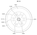
- the branch circuit 0202 and its surroundings will be described in detail with reference to Figures 3A and 3B.
- Figure 3A is a side cross-sectional view
- Figure 3B is a plan view.
- the branch circuit 0202 has the role of transmitting microwaves transmitted from the circular waveguide 0106 to the ring resonator 0201, and is composed of a rectangular waveguide 0301 branched into six by phase adjustment means 0304, a matching rod (first matching section) 0302 that suppresses reflected waves at the branch point between the circular waveguide 0106 and the rectangular waveguide 0301, and a matching ridge (second matching section) 0303 that suppresses reflections from the connection surface with the ring resonator 0201, etc.
- the rectangular waveguide 0301 is arranged with six phase adjustment means 0304 branching out at equal intervals of 60 degrees in the azimuth direction to branch microwave power in six directions, but the number of branches may be an integer equal to or greater than 3.
- the rectangular waveguide 0301 is sized to operate in the TE 10 mode, which is the lowest order mode of a rectangular waveguide.
- the matching rod 0302 is cylindrical and arranged coaxially with the circular waveguide 0106. By optimizing its diameter and height, it is possible to suppress reflected waves at the connection surface between the circular waveguide 0106 and the multiple rectangular waveguides 0301. Similarly, the position, height, and width of the matching ridge 0303 can be adjusted to suppress reflected waves caused by discontinuous surfaces after the rectangular waveguide 0301.
- the microwave power incident from the circular waveguide 0106 can be efficiently transmitted to the inside of the processing chamber.
- the matching rod 0302 and matching ridge 0303 may be omitted.
- the coaxial line 0110 connected to the ring resonator 0201 has a microwave introduction window 0111 as described in FIG. 2 attached to its inner circumference, and the bottom surface of the coaxial line 0110 is closed, but in FIG. 3A, the microwave introduction window 0111 is omitted, and the bottom surface of the coaxial line 0110 is shown open.
- a desired electromagnetic field can be obtained by using a resonator that resonates with the desired electromagnetic field.
- Fig. 4A shows a longitudinal section
- Fig. 4B shows an M-M cross section of Fig. 4A.
- the TM110 mode can be considered as a mode in which a rectangular waveguide of one wavelength length operating in the lowest order TE10 mode is bent into a ring shape.
- the wave number vector which indicates the direction of wave travel, only has azimuth and radial components, and does not have a component parallel to the central axis.
- the resonance condition of the TM110 mode ring resonator does not depend on the dimension parallel to the central axis (H in FIG. 4A), but only on the inner radius (a in FIG. 4A) and the outer radius (b in FIG. 4A) of the ring. Since a circularly polarized wave is supplied to the circular waveguide, the electromagnetic field in the ring resonator 0201 shown in FIG. 4A and FIG. 4B rotates in time in the azimuth direction.
- Equation 1 The dimensions of the ring resonator can be found by solving this equation (Equation 1).
- there are no structures that are discontinuous in the azimuth direction on the path from the coaxial line to the plasma processing chamber, and the m 1 distribution within the ring resonator is maintained to excite the coaxial line.
Abstract
プラズマ処理装置の処理室内でのプラズマの均一性をより向上させることを可能にする。このため、被処理基板0113を載置する試料台を内部に備えた試料室0112と、試料室の内部に磁界を発生させる磁界発生手段0116と、マイクロ波電力を発生させるマイクロ波電力源0101と、マイクロ波電力を搬送するマイクロ波電力搬送部0103,0106と、搬送されたマイクロ波電力を誘電体窓を介して処理室の内部に供給するマイクロ波立体回路部とを備えたプラズマ処理装置において、マイクロ波立体回路部を、マイクロ波電力搬送部により搬送されたマイクロ波電力を複数の方位角方向に分岐する分岐回路0202と、この分岐回路で複数の方位角方向に分岐されたマイクロ波電力を共振させるリング共振器0201と、このリング共振器で共振させたマイクロ波電力を誘電体窓を介して処理室の内部に供給する同軸線路部0110とを備えて構成した。
Description
本発明は、マイクロ波と静磁界の相互作用を用いてプラズマを発生させるプラズマ処理装置に関し、特に、プラズマ処理室内での該マイクロ波の進行方向が該静磁界の方向に対して略垂直であり、かつ該マイクロ波電界の方向が該静磁界の方向に対して略垂直となるよう、静磁界とマイクロ波立体回路系を構成した装置において、処理室内のプラズマ密度分布の観点でマイクロ波立体回路系を最適にした装置に関する。
半導体集積回路素子の生産にプラズマ処理装置が用いられている。素子の性能向上とコスト低減のため、素子の微細化が進展してきた。従来は素子の2次元的な微細化により、1枚の被処理基板より製造できる素子数が増加して素子1個あたりの製造コストが下がると共に、配線長短縮など小型化の効果で性能向上も図れてきた。しかし半導体素子の寸法が原子の寸法に近いナノメートルオーダーとなると、2次元的な微細化の難易度が著しく高まり、新材料や3次元的な素子構造の適用など、対応が為されている。これらの構造変更により、製造の難易度が上がると共に製造工程は増加し、製造コストの増大が深刻な問題となっている。
製造途中の半導体集積回路素子に微小な異物や汚染物質が付着すると、致命的な欠陥となるため、半導体集積回路素子は異物や汚染物質を排除し温度や湿度を最適に制御したクリーンルーム内で製造される。素子の微細化に伴い、製造に必要なクリーンルームの清浄度は高くなり、クリーンルームの建設や維持運用に莫大な費用が必要となる。そのため、クリーンルーム空間を効率よく利用して生産することが求められる。この観点から、半導体製造装置は小型化と低コスト化が厳しく求められている。
また被処理基板に対するプラズマ処理の面内均一性も重要である。半導体集積回路素子の製造には被処理基板として直径300mmの円盤状のシリコンウェハが用いられることが多い。このシリコンウェハ上に多数の半導体集積回路素子を作成することが多いが、プラズマ処理の面内均一性が悪いと、1枚のシリコンウェハから取得できる仕様を満足した良品が少なくなる場合がある。同様に各被処理基板ごとのプラズマ処理の安定性も重要である。プラズマ処理の品質が安定せず、例えば経時的に品質が変化する場合は、同様に良品の割合が低下する場合がある。
電磁波によりプラズマを発生するプラズマ処理装置において、電磁波として周波数が数GHz程度、典型的には2.45GHzのマイクロ波を用いた装置が広く用いられている。特にマイクロ波と静磁界を組合わせて起きる電子サイクロトロン共鳴(Electron Cyclotron Resonance、以下ECRと称する)現象を用いた装置があり、この装置では、極低圧などプラズマの生成が通常は困難な条件でも比較的安定にプラズマを生成できる、静磁界の分布によりプラズマの分布を制御できるなどの優れた特徴を持っている。
マイクロ波と静磁界の相互作用として、高域混成共鳴(Upper Hybrid Resonance、以下UHRと称する)という現象も知られている。静磁界と垂直な方向に伝搬し、かつマイクロ波電界が静磁界に垂直なマイクロ波(X波と称する)がプラズマ中の電子と共鳴し、マイクロ波のエネルギーが電子に強く吸収される現象である。ECRに比べ弱い静磁界でUHRは発生することが知られている。この現象を積極的に活用したプラズマ処理装置の公知例は少ないが、従来例として以下の発明がある。
特許文献1では略円筒状処理室の中心軸方向と略平行に静磁界を印加し、側面からマイクロ波を投入している。さらに該マイクロ波の電界は処理室の中心軸方向に略垂直としている。これらの施策により、処理室内のプラズマ中にX波を励起して、UHRを活用している。さらに該処理室の該静磁界と略垂直となる面の一方に被処理基板を設置する電極、他方の面にアース電極(対向アースと称する)を設けている。これにより後述のRFバイアスを効率よく被処理基板に印加できる構成としている。ECRを用いた装置に比べ、弱い静磁界で共鳴を起こすことができるため、静磁界を発生させるための電磁石による消費電力を低減できる、電磁石の小型化が可能で配置の自由度が増すなどの利点がある。
さらに特許文献1では対向アースを複数の支柱で保持し、これらの支柱などの不連続部に起因するマイクロ波の反射を抑制するための構造も含むマイクロ波の立体回路系により処理室にマイクロ波を効率よく投入している。
マイクロ波を用いたプラズマ処理装置では、マイクロ波の発振器としてマグネトロンが広く用いられるが、最近は固体素子を用いた発振器も用いられるようになってきた。固体素子を用いた発振器では発振周波数や出力がマグネトロンに比べ安定する、種々の変調が容易に加えられる等の利点がある。またマイクロ波電力の伝送に方形導波管、円形導波管、同軸線路などが用いられる。そのほかマイクロ波発振器を保護するためのアイソレータ、負荷とのインピーダンス不整合を防止するための自動整合器を組み合わせて用いることが多い。
また被処理基板にRFバイアス電力を与えて、プラズマ処理の品質を高めることができる。例えばプラズマエッチング処理の場合、周波数400kHzから13.56MHz程度のRFバイアスにより、イオンと電子の質量差に起因する直流バイアス電圧を被処理基板に生じさせ、この直流バイアス電圧でプラズマ中のイオンを引き込んで、加工形状の垂直性や加工速度を高める等により、プラズマ処理の品質を高めることができる。
一般にマイクロ波の伝送経路に不連続部があると、反射波が生じる。マイクロ波をプラズマ処理室に投入する構造においても、例えば円形導波管をステップ状に拡大するとこれに起因して反射波が生じる。プラズマ処理室内にプラズマ均一性の観点から最適な電磁界分布を実現するための構造が複雑化すると、各部で生じる反射波の影響でマイクロ波電力を処理室内に効率よく伝送できなくなる場合がある。そのため構造は極力単純化することが望ましいが、望ましい電磁界との両立が難しくなることが多い。対策として上述の整合器が用いられるが、負荷との不整合の度合いが大きすぎると、これに対応した広い整合範囲の確保が難しくなる場合があるほか、整合器と負荷との間に大きな定在波が生じて、これによる異常放電や電力損失が問題となる場合がある。
特許文献1に開示された実施例を適用すると、プラズマ生成条件によってはプラズマが処理室側壁部の近傍に過度に局在し、被処理基板近傍のプラズマ密度が低くなる場合があることが分かった。発明者等がこの原因を調査した結果、意図していたマイクロ波の伝搬モードの割合が低く、方位角方向に多数の変化をする高次モードの割合が大きくなる場合があることが原因であると判明した。意図していたマイクロ波の伝搬モードは方位角方向の変化数(mと称する)が1であったが、対向アースの保持に用いる複数の支柱の影響などにより、m=5などの高次モードが多く発生する場合があることが分かった。
プラズマ処理室の内部におけるプラズマ密度の均一性をより向上させるためには、マイクロ波立体回路の構造を工夫してm=1のモードの割合を増やし、mが大きな高次モードの割合を減らすことが必要になる。
本発明は、上記した従来技術の課題を解決して、処理室内でのプラズマの均一性をより向上させることを可能にするプラズマ処理装置を提供するものである。
上記した課題を解決するために、本発明では、被処理基板を載置する試料台を内部に備えた試料室と、試料室の内部に磁界を発生させる磁界発生手段と、マイクロ波電力を発生させるマイクロ波電力源と、このマイクロ波電力源で発生したマイクロ波電力を搬送するマイクロ波電力搬送部と、このマイクロ波電力搬送部により搬送されたマイクロ波電力を誘電体窓を介して処理室の内部に供給するマイクロ波立体回路部とを備えたプラズマ処理装置において、マイクロ波立体回路部を、マイクロ波電力搬送部により搬送されたマイクロ波電力を複数の方位角方向に分岐する分岐回路部と、この分岐回路部の周囲に配置されて分岐回路部で複数の方位角方向に分岐されたマイクロ波電力を共振させるリング共振器と、このリング共振器に接続してリング共振器で共振させたマイクロ波電力を誘電体窓を介して処理室の内部に供給する同軸線路部とを備えて構成した。
本発明によれば、上記構成のマイクロ波立体回路を用いることで、m=1のマイクロ波を同軸線路内およびプラズマ処理室内に励振することができるようになり、従来技術と比べて処理室内でのプラズマの均一性をより向上させることが可能になった。
本発明は、略円柱状のプラズマ処理室を備え、マイクロ波電力を該プラズマ処理室の側面から投入してプラズマを発生させるプラズマ処理装置において、マイクロ波の半径方向に進行するマイクロ波電力の割合が小さく、生成されるプラズマが側面内壁付近に過度に局在して、該プラズマ処理室の中心軸付近のプラズマ密度が低くなる場合があるという課題を、マイクロ波の方位角方向への進行を抑制して半径方向の進行成分を増やすため、方位角方向依存性mの値が1のモードで共振するリング共振器を用いてマイクロ波を処理室に投入する構成とすることで解決して、プラズマ処理室内でのプラズマの均一性をより向上させることを可能にするプラズマ処理装置を実現したものである。
また、先に説明した従来技術におけるプラズマ処理装置では、プラズマ生成条件によってはプラズマが処理室側壁部の近傍に過度に局在し、被処理基板近傍のプラズマ密度が低くなる場合がある。これに対して、本発明では、マイクロ波立体回路の構造を工夫してm=1のモードの割合を増やし、mが大きな高次モードの割合を減らせるような構成を可能にした。これにより、本発明では、従来技術における課題を解決して、処理室内でのプラズマの均一性をより向上させることを可能にするプラズマ処理装置を実現したものである。
特許文献1の実施例に開示されている従来技術におけるプラズマ処理装置の構成を図1により説明する。この従来技術は、エッチング処理を行うプラズマ処理装置100である。マイクロ波源0101より発生した周波数2.45GHzのマイクロ波は、図示しないアイソレータ、自動整合器0102を介して方形導波管0103、伝送方向を90度変えるコーナを兼ねた円矩形変換器0104を介して、円形導波管0106に伝送される。円形導波管0106内には円偏波発生器0105が装荷されている。円偏波発生器0105は直線偏波として入射したマイクロ波を円偏波に変換する機能を持つ。マイクロ波を円偏波化することで、方位角方向に均一なプラズマを生成することができる。さらにマイクロ波は拡大部0107を介して同軸線路0110に伝送される。同軸線路0110内にマイクロ波電界分布を模式的に矢印で表示している。
拡大部0107の下部には複数の支柱0108を介して外部に固定された対向アース0109がある。対向アース0109の下部、同軸線路0110の内側に円柱状のマイクロ波導入窓0111がある。マイクロ波導入窓の材質はマイクロ波に対する損失が小さく、プラズマ耐性がありさらにプラズマ処理に悪影響を及ぼし難いことが望ましく、石英を用いた。
拡大部0107の内部の外周部で天井壁および側壁に接する部分には、リング状の整合部材0119が配置されている。
対向アース0109、マイクロ波導入窓0111で構成された領域付近がプラズマ処理室0112となる。プラズマ処理室内には直径300mmの被処理基板0113を戴置するための基板電極0114がある。基板電極0114にはRF電源0115が自動整合器0117を介して接続され、被処理基板0113にRFバイアスを印加することができる。RF電源0115として発振周波数が400kHzのものを用いた。さらにこれらの機構の周囲にはヨークを備えた多段のソレノイドコイル0116が設けられ、プラズマ処理室0112内に静磁界を加えることができる。
被処理基板0113は円盤状であり、これに対応して装置は基本的に被処理基板0113の中心軸と軸を共有する軸対称な構造としている。すなわち略円柱状のプラズマ処理室0112の中心軸と同軸に、基盤電極0114、同軸線路0110、対向アース0109、拡大部0107、円形導波管0106、およびソレノイドコイル0116が配置されている。
そのほかプラズマ処理室0112には図示しないガス供給系、真空排気系が接続され、所定の流量の処理ガスを所定の圧力を保持しながら供給および排気することができる。
対向アース0109は外部構造と固定する必要があるほか、冷却等の温度調整機構、また対向アース部からのガス供給機構を内蔵しており、外部と複数の支柱0108で固定されている。冷媒やガスの流路が支柱0108内に設けられている。さらに支柱0108により対向アース0109は外部と電気的につながっており、電位の安定化が図れる。
図1に示す従来例のプラズマ処理装置100で実験を行うと、プラズマ処理室0112内に発生したプラズマは主にマイクロ波導入窓0111の内面近傍に過度に局在し、処理室の中心軸付近の密度が低くなる場合があることが分かった。そのため被処理基板0113に施すプラズマエッチング処理の処理速度が遅くなる場合があった。
この原因を発明者が検討したところ、投入したマイクロ波が主に方位角方向に進行して、半径方向に進行する成分の割合が小さいためであることが分かった。さらにマイクロ波が方位角方向に進行する主な原因は、対向アース0109を保持する複数の支柱0108にあることが分かった。支柱0108は対向アース0109を側面から半径方向に支えており、この影響で方位角方向の依存性mの大きな成分が励起されていることがわかった。
一般に境界の無い真空中を平面波として伝搬するマイクロ波は光速で伝搬し、波の進行方向に対する波長は光速を周波数で除した値となる。完全導体面が空間中にあると、完全導体表面に対して電界ベクトルが垂直になる境界条件を満足するよう、マイクロ波は反射する。導波管等で構成されたマイクロ波の立体回路系では、導波管内壁を完全導体として解析することができ、境界条件を満足するよう内壁での反射を繰り返して、それぞれの波が重畳して電磁界分布が決まる。
リング共振器内でも上記と同様に、内壁で反射を繰り返して、内部のマイクロ波電磁界が決まる。波の進行方向は波数ベクトルで評価でき円柱座標系(r、θ、z)で考えて、半径(r)方向、方位角(θ)方向、高さ(z)方向の各成分を持つ。後述のTM110モードリング共振器内では、波数ベクトルはz成分がゼロであり、半径方向と方位角方向に伝搬し、高さ方向には伝搬しない。方位角方向の依存性mは方位角方向の1周(360度)内に波がm波長分存在することを示し、m=1の場合、方位角方向に1周期分の変化を示す。
以上の考察に基づき、方位角方向の依存性mの小さい成分を処理室内に励起するマイクロ波立体回路の構造を検討した。ただしマイクロ波のプラズマ処理室0112への投入に用いる円形導波管0106の最低次モードがm=1であることを考慮して、処理室内にm=1のマイクロ波電磁界を励起する構造を検討した。
この検討結果に基づく本実施例に係るプラズマ処理装置200の構成を図2に示し、その部分的な詳細な構成を図3A乃至図4Bを用いて説明する。
図2に示した本実施例に係るプラズマ処理装置200の構成において図1に示す従来技術のプラズマ処理装置100との違いは、マイクロ波電力をプラズマ処理室0112に投入する分岐回路0202とリング共振器0201,同軸線路0110、中央に凸状の部分0204が形成された対向アース0203を備えて構成されるマイクロ波立体回路部分である。分岐回路0202を形成する整合ロッド0302、整合リッジ0303,位相調整手段0304については、図3A及び図3Bを用いて説明する。それ以外の構成で図1と同じ部品番号を付したものは、図1で説明した従来のプラズマ処理装置100の構成と同じであり、本実施例と共通する部分については説明を省略する。
図2に示した本実施例に係るプラズマ処理装置200の構成において、円偏波発生器0105で円偏波化され、円形導波管0106で伝送されたマイクロ波は、円形導波管0106の直下で対向アース0203の凸部の上面0204に形成された分岐回路0202で分岐され、対向アース0203の凸部の側面0205の周囲に形成されたリング共振器0201を励振する。さらにリング共振器0201には同軸線路0110が接続されマイクロ波導入窓0111を介してプラズマ処理室0112に投入される。
分岐回路0202とその周辺の詳細を図3Aと図3Bとを用いて説明する。図3Aは側面断面図、図3Bは平面図である。分岐回路0202は円形導波管0106から伝送されたマイクロ波をリング共振器0201に伝送する役割を持ち、位相調整手段0304により6分岐された方形導波管0301、円形導波管0106と方形導波管0301分岐部での反射波を抑制する整合ロッド(第1の整合部)0302、およびリング共振器0201との接続面等による反射を抑制する整合リッジ(第2の整合部)0303からなる。
方形導波管0301は6個の位相調整手段0304により方位角方向に均等に60度毎の間隔で分岐されて配置され、6方向にマイクロ波電力を分岐しているが、分岐の数は3以上の整数であればよい。方形導波管0301は方形導波管の最低次モードであるTE10モードで動作する寸法とした。
整合ロッド0302は円形導波管0106と同軸に配置された円筒形状で、直径と高さを最適化することで、円形導波管0106と複数の方形導波管0301との接続面での反射波を抑制することができる。同様に整合リッジ0303はその位置と高さ及び幅を調節して方形導波管0301以降の不連続面に起因する反射波を抑制することができる。
これらの整合ロッド0302、整合リッジ0303の形状パラメータを最適に調節することにより、円形導波管0106から入射したマイクロ波電力を効率よく処理室内まで伝送することができる。ただし、マイクロ波の反射が許容できる場合には整合ロッド0302、整合リッジ0303は省略しても良い。
なお、リング共振器0201に接続している同軸線路0110の内周側には図2で説明したようなマイクロ波導入窓0111が装着され、同軸線路0110の下面は閉じているが、図3Aにおいては、マイクロ波導入窓0111の表示を省略し、同軸線路0110の下面は解放した状態で表示してある。
一般に共振器の内部では境界条件を満足する電磁界のみが存在できる。そのため所望の電磁界で共振する共振器を用いることで、所望の電磁界を得ることができる。本実施例では図4A及び図4Bに示す電界分布(TM110モードと称する)で共振するリング共振器0201を用いた。これにより所望のm=1を満たす電磁界を得ることができる。
図4Aは縦断面、図4Bは図4AにおけるM-M断面矢視図を示す。TM110モードは最低次のTE10モードで動作する一波長分の長さの方形導波管をリング状に屈曲させたモードと考えることができる。
図4Bに示すように方位角方向一周で、電界ベクトルも一周分の変化を示し、m=1のモードとなっている。また波の進行方向を示す波数ベクトルは方位角方向と半径方向成分のみを持ち、中心軸と平行方向の成分を持たない。
従ってTM110モードリング共振器の共振条件は中心軸と平行方向の寸法(図4A中のH)に依存せず、リングの内側半径(図4A中のa)と外側半径(図4A中のb)にのみ依存する。円形導波管には円偏波が供給されているので、図4A及び図4Bに示すリング共振器0201内の電磁界は方位角方向に時間的に回転する。
TM110モードで共振するリング共振器は境界条件を考慮した結果、以下の式(数1)を満足する。この式(数1)を解くことでリング共振器の寸法を求めることができる。

リング共振器0201の下部には同軸線路0110が接続されており、リング共振器0201内でm=1のモードに調整されたマイクロ波で同軸線路0110が励振される。前述の特許文献1に開示されている構成では、対向アース保持のため同軸線路部のマイクロ波入射面付近に複数の支柱があり、この影響でmの大きな波が生じた。本実施例では同軸線路からプラズマ処理室に至る経路に方位角方向に不連続な構造物は無く、リング共振器内のm=1分布が維持されて同軸線路が励振される。プラズマ処理室内にも方位角方向に不連続な構造物は無く、マイクロ波導入窓を介してm=1の分布でマイクロ波は処理室に投入することができる。
本実施例によれば、上記に説明したような構成のマイクロ波立体回路を用いることで、m=1のマイクロ波を同軸線路内およびプラズマ処理室内に励振することができるようになったので、プラズマ処理室の内部におけるプラズマ密度の均一性をより向上させることができるようになった。
以上、本発明者によってなされた発明を実施例に基づき具体的に説明したが、本発明は前記実施例に限定されるものではなく、その要旨を逸脱しない範囲で種々変更可能であることは言うまでもない。例えば、上記した実施例は本発明を分かりやすく説明するために詳細に説明したものであり、必ずしも説明した全ての構成を備えるものに限定されるものではない。また、各実施例の構成の一部について、他の構成の追加・削除・置換をすることが可能である。
0101…マイクロ波源、0102…自動整合器、0103…方形導波管、0104…円矩形変換器、0105…円偏波発生器、0106…円形導波管、0107…拡大部、0108…支柱、0109…対向アース、0110…同軸線路、0111…マイクロ波導入窓、0112…プラズマ処理室、0113…被処理基板、0114…基板電極、0115…RF電源、0116…ソレノイドコイル、0201…リング共振器、0202…分岐回路、0203…対向アース、0204…凸状の部分、0301…6分岐された方形導波管、0302…整合ロッド、0303…整合リッジ、0304…位相調整手段。
Claims (5)
- 被処理基板を載置する試料台を内部に備えた処理室と、
前記処理室の内部に磁界を発生させる磁界発生手段と、
マイクロ波電力を発生させるマイクロ波電力源と、
前記マイクロ波電力源で発生した前記マイクロ波電力を搬送するマイクロ波電力搬送部と、
前記マイクロ波電力搬送部により搬送された前記マイクロ波電力を誘電体窓を介して前記処理室の内部に供給するマイクロ波立体回路部と
を備えたプラズマ処理装置であって、
前記マイクロ波立体回路部は、
前記マイクロ波電力搬送部により搬送された前記マイクロ波電力を複数の方位角方向に分岐する分岐回路部と、
前記分岐回路部の周囲に配置されて前記分岐回路部で複数の方位角方向に分岐された前記マイクロ波電力を共振させるリング共振器と、
前記リング共振器に接続して前記リング共振器で共振させた前記マイクロ波電力を前記誘電体窓を介して前記処理室の内部に供給する同軸線路部とを備えていることを特徴とするプラズマ処理装置。 - 請求項1記載のプラズマ処理装置であって、
前記マイクロ波立体回路部の前記分岐回路部と前記リング共振器とは、前記分岐回路部の周囲に等間隔で配置された複数の方形導波管を介して接続されていることを特徴とするプラズマ処理装置。 - 請求項1記載のプラズマ処理装置であって、
前記マイクロ波電力搬送部は、最低次のTE11モードの前記マイクロ波電力が伝搬する円形導波管を介して前記分岐回路部と接続されており、前記円形導波管の中心軸と前記分岐回路部の中心軸とは同軸であることを特徴とするプラズマ処理装置。 - 請求項1記載のプラズマ処理装置であって、
前記分岐回路部は、前記マイクロ波電力搬送部と前記分岐回路部とが接合する部分における反射波を抑制する第1の整合部と、前記分岐回路部と前記リング共振器との接続面等による反射を抑制する第2の整合部とを更に備えていることを特徴とするプラズマ処理装置。 - 請求項1記載のプラズマ処理装置であって、
前記分岐回路部は設置されており、前記分岐回路部の一部が前記リング共振器の一部を形成していることを特徴とするプラズマ処理装置。
Priority Applications (1)
| Application Number | Priority Date | Filing Date | Title |
|---|---|---|---|
| KR1020247002378A KR20240055722A (ko) | 2022-10-19 | 2023-07-24 | 플라스마 처리 장치 |
Applications Claiming Priority (2)
| Application Number | Priority Date | Filing Date | Title |
|---|---|---|---|
| JP2022167445 | 2022-10-19 | ||
| JP2022-167445 | 2022-10-19 |
Publications (1)
| Publication Number | Publication Date |
|---|---|
| WO2024084762A1 true WO2024084762A1 (ja) | 2024-04-25 |
Family
ID=90737465
Family Applications (1)
| Application Number | Title | Priority Date | Filing Date |
|---|---|---|---|
| PCT/JP2023/026919 WO2024084762A1 (ja) | 2022-10-19 | 2023-07-24 | プラズマ処理装置 |
Country Status (2)
| Country | Link |
|---|---|
| KR (1) | KR20240055722A (ja) |
| WO (1) | WO2024084762A1 (ja) |
Citations (2)
| Publication number | Priority date | Publication date | Assignee | Title |
|---|---|---|---|---|
| JP2012190899A (ja) * | 2011-03-09 | 2012-10-04 | Hitachi High-Technologies Corp | プラズマ処理装置 |
| JP7139528B2 (ja) * | 2020-04-27 | 2022-09-20 | 株式会社日立ハイテク | プラズマ処理装置 |
Family Cites Families (1)
| Publication number | Priority date | Publication date | Assignee | Title |
|---|---|---|---|---|
| JP7001456B2 (ja) | 2017-12-19 | 2022-01-19 | 株式会社日立ハイテク | プラズマ処理装置 |
-
2023
- 2023-07-24 KR KR1020247002378A patent/KR20240055722A/ko unknown
- 2023-07-24 WO PCT/JP2023/026919 patent/WO2024084762A1/ja unknown
Patent Citations (2)
| Publication number | Priority date | Publication date | Assignee | Title |
|---|---|---|---|---|
| JP2012190899A (ja) * | 2011-03-09 | 2012-10-04 | Hitachi High-Technologies Corp | プラズマ処理装置 |
| JP7139528B2 (ja) * | 2020-04-27 | 2022-09-20 | 株式会社日立ハイテク | プラズマ処理装置 |
Also Published As
| Publication number | Publication date |
|---|---|
| KR20240055722A (ko) | 2024-04-29 |
Similar Documents
| Publication | Publication Date | Title |
|---|---|---|
| US6158383A (en) | Plasma processing method and apparatus | |
| KR101711713B1 (ko) | 마이크로파 방사 기구, 마이크로파 플라즈마원 및 표면파 플라즈마 처리 장치 | |
| JP3792089B2 (ja) | プラズマプロセス装置 | |
| JPH10134996A (ja) | プラズマ処理装置 | |
| KR100321325B1 (ko) | 플라즈마생성방법및장치와그것을사용한플라즈마처리방법및장치 | |
| JP7001456B2 (ja) | プラズマ処理装置 | |
| JP7139528B2 (ja) | プラズマ処理装置 | |
| JP4134226B2 (ja) | 分配器および方法、プラズマ処理装置および方法、並びに、lcdの製造方法 | |
| JP2012190899A (ja) | プラズマ処理装置 | |
| JP4678905B2 (ja) | プラズマ処理装置 | |
| WO2021220459A1 (ja) | プラズマ処理装置 | |
| JP6991934B2 (ja) | プラズマ処理装置 | |
| WO2024084762A1 (ja) | プラズマ処理装置 | |
| JP4600928B2 (ja) | マイクロ波方向性結合器、プラズマ発生装置及びプラズマ処理装置 | |
| KR102521817B1 (ko) | 플라스마 처리 장치 | |
| JP4900768B2 (ja) | プラズマ発生装置及びプラズマ処理装置 | |
| JP4017098B2 (ja) | プラズマ発生装置及びプラズマ処理装置 | |
| JP2932946B2 (ja) | プラズマ処理装置 | |
| JP6700127B2 (ja) | マイクロ波プラズマ処理装置 | |
| JP2007018819A (ja) | 処理装置および処理方法 | |
| JP5382958B2 (ja) | プラズマ発生装置及びプラズマ処理装置 | |
| JP3047801B2 (ja) | プラズマ処理方法及び装置 | |
| US20230238217A1 (en) | Plasma processing apparatus | |
| JP3047802B2 (ja) | プラズマ処理装置 | |
| JPH10107011A (ja) | プラズマ処理装置 |