WO2024071400A1 - 導電性接着剤層 - Google Patents
導電性接着剤層 Download PDFInfo
- Publication number
- WO2024071400A1 WO2024071400A1 PCT/JP2023/035699 JP2023035699W WO2024071400A1 WO 2024071400 A1 WO2024071400 A1 WO 2024071400A1 JP 2023035699 W JP2023035699 W JP 2023035699W WO 2024071400 A1 WO2024071400 A1 WO 2024071400A1
- Authority
- WO
- WIPO (PCT)
- Prior art keywords
- metal particles
- adhesive layer
- conductive adhesive
- particles
- mass
- Prior art date
- Legal status (The legal status is an assumption and is not a legal conclusion. Google has not performed a legal analysis and makes no representation as to the accuracy of the status listed.)
- Ceased
Links
Images

Classifications
-
- H—ELECTRICITY
- H01—ELECTRIC ELEMENTS
- H01B—CABLES; CONDUCTORS; INSULATORS; SELECTION OF MATERIALS FOR THEIR CONDUCTIVE, INSULATING OR DIELECTRIC PROPERTIES
- H01B1/00—Conductors or conductive bodies characterised by the conductive materials; Selection of materials as conductors
- H01B1/20—Conductive material dispersed in non-conductive organic material
- H01B1/22—Conductive material dispersed in non-conductive organic material the conductive material comprising metals or alloys
-
- C—CHEMISTRY; METALLURGY
- C09—DYES; PAINTS; POLISHES; NATURAL RESINS; ADHESIVES; COMPOSITIONS NOT OTHERWISE PROVIDED FOR; APPLICATIONS OF MATERIALS NOT OTHERWISE PROVIDED FOR
- C09J—ADHESIVES; NON-MECHANICAL ASPECTS OF ADHESIVE PROCESSES IN GENERAL; ADHESIVE PROCESSES NOT PROVIDED FOR ELSEWHERE; USE OF MATERIALS AS ADHESIVES
- C09J201/00—Adhesives based on unspecified macromolecular compounds
-
- C—CHEMISTRY; METALLURGY
- C09—DYES; PAINTS; POLISHES; NATURAL RESINS; ADHESIVES; COMPOSITIONS NOT OTHERWISE PROVIDED FOR; APPLICATIONS OF MATERIALS NOT OTHERWISE PROVIDED FOR
- C09J—ADHESIVES; NON-MECHANICAL ASPECTS OF ADHESIVE PROCESSES IN GENERAL; ADHESIVE PROCESSES NOT PROVIDED FOR ELSEWHERE; USE OF MATERIALS AS ADHESIVES
- C09J7/00—Adhesives in the form of films or foils
- C09J7/30—Adhesives in the form of films or foils characterised by the adhesive composition
-
- C—CHEMISTRY; METALLURGY
- C09—DYES; PAINTS; POLISHES; NATURAL RESINS; ADHESIVES; COMPOSITIONS NOT OTHERWISE PROVIDED FOR; APPLICATIONS OF MATERIALS NOT OTHERWISE PROVIDED FOR
- C09J—ADHESIVES; NON-MECHANICAL ASPECTS OF ADHESIVE PROCESSES IN GENERAL; ADHESIVE PROCESSES NOT PROVIDED FOR ELSEWHERE; USE OF MATERIALS AS ADHESIVES
- C09J9/00—Adhesives characterised by their physical nature or the effects produced, e.g. glue sticks
- C09J9/02—Electrically-conducting adhesives
Definitions
- the present invention relates to a conductive adhesive layer.
- Conductive adhesive layers have traditionally been used to connect electronic components.
- One such conductive adhesive layer is known to be an alloy of low-melting-point metal particles and high-melting-point metal particles, which can replace high-temperature solder and provide connection stability (Patent Document 1).
- the present invention aims to solve these problems by providing a conductive adhesive layer that has sufficient adhesive strength for a variety of adherends, even under low-temperature, short-time compression processing conditions.
- the present invention was completed based on this knowledge.
- the present invention provides a conductive adhesive layer that contains a binder component and metal particles A having a melting point of 170°C or less, with the metal A protruding from the surface.
- the conductive adhesive layer contains a binder component and metal particles A with a melting point of 170°C or less, and because the metal particles A protrude from the surface of the conductive adhesive layer, it can exhibit high adhesive strength to a variety of adherends even under low temperature and short compression processing conditions.
- the conductive adhesive layer preferably contains, in addition to the metal particles A, metal particles B that can be alloyed with metal particles A. By including metal particles B, the electrical conductivity and adhesive strength of the conductive adhesive layer can be improved.
- the conductive adhesive layer further contains solder particles C in addition to the metal particles A.
- solder particles C electrical conductivity in the thickness direction can be improved.
- the metal particles A are preferably spherical. When the metal particles A are spherical, the metal particles A are more likely to protrude from the surface of the conductive adhesive layer, making it easier to achieve high adhesion strength.
- the metal particles B are preferably dendritic or flaky. When the metal particles B are dendritic or flaky, it becomes easier to achieve high adhesion strength.
- solder particles C are spherical. By making the solder particles C spherical, the electrical conductivity in the thickness direction can be stabilized without variation.
- the median diameter (D50) of the metal particles A is larger than the film thickness of the conductive adhesive layer.
- the median diameter (D50) of the metal particles A is larger than the film thickness of the conductive adhesive layer, it becomes easier to exhibit adhesion strength under low-temperature, short-time compression processing conditions.
- the thickness of the conductive adhesive layer is preferably 1 to 50 ⁇ m.
- the conductive adhesive layer of the present invention can exert sufficient adhesive strength to various adherends even under low temperature and short pressure processing conditions. In particular, it can exert sufficient adhesive strength even when the adherend is a metal plate or Ni-Au plated.
- FIG. 2 is a cross-sectional view showing one embodiment of a conductive adhesive layer of the present invention.
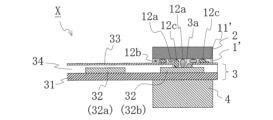
- 1 is a cross-sectional view showing one embodiment of a printed wiring board with a reinforcing member to which a conductive adhesive layer of the present invention is applied.
- the conductive adhesive layer of the present invention includes at least a binder component and metal particles A having a melting point of 170° C. or less, and the metal particles A protrude from the surface of the conductive adhesive layer.
- metal particles A the metal particles having a melting point of 170° C. or less are referred to as "metal particles A”.
- protruding from the surface of the conductive adhesive layer refers to a state in which the conductive particles of the adhesive portion composed of the binder component protrude to a position outside the horizontal plane (specifically, the plane obtained by averaging the height of the surface) of the area where the conductive particles do not protrude before the binder component flows, and for example, an embodiment in which the median diameter (D50) of the metal particles A or the particle thickness described later is larger than the thickness of the conductive adhesive layer.
- the thickness of the conductive adhesive layer refers to the average thickness (for example, the thickness T shown in FIG. 1) in the area where the conductive particles of the adhesive portion composed of the binder component do not protrude before the binder component flows.
- the metal particles A may or may not be covered by the conductive adhesive layer.
- the conductive adhesive layer may be an anisotropic conductive adhesive layer or an isotropic conductive adhesive layer.
- the layer when metal particles A are mainly responsible for the conductivity of the conductive adhesive layer, the layer will be an anisotropic conductive adhesive layer, and when the metal particles A and other conductive particles (for example, metal particles B described below) are mixed in a balanced manner, the layer will be an isotropic conductive adhesive layer.
- the conductive adhesive layer preferably contains metal particles B that can be alloyed with metal particles A and solder particles C.
- metal particles B that can be alloyed with metal particles A and solder particles C in addition to metal particles A, it becomes easier to exert adhesive strength to various adherends even under low temperature and short pressure processing conditions.
- FIG 1 shows one embodiment of the conductive adhesive layer of the present invention.
- the conductive adhesive layer (1) contains a binder component (11), metal particles A (12a), metal particles B (12b) that can be alloyed with the metal particles A, and solder particles C (12c).
- the metal particles A (12a) protrude from the surface of the adhesive layer composed of the binder component (11).
- the metal particles A have a melting point of 170° C. or less, preferably 160° C. or less, and more preferably 150° C. or less.
- the lower limit of the melting point is not particularly limited, but is preferably 130° C. or more.
- the metal particles A are preferably an alloy containing tin (melting point: 232°C) and bismuth (melting point: 271°C), and may contain other metals in addition to tin and bismuth as long as the melting point is within a range of 170°C or less.
- the mass ratio of tin:bismuth in the metal particles A is preferably 30:70 to 80:20, more preferably 35:65 to 60:40, and particularly preferably 40:60 to 45:55.
- the above mass ratio of tin:bismuth makes it easy to adjust the melting point of the metal particles A to within the range of 130°C to 170°C.
- the median diameter (D50) of the metal particles A is preferably larger than the thickness of the conductive adhesive layer, and is preferably 70 to 500% of the thickness of the conductive adhesive layer, more preferably 100 to 400%, and particularly preferably 150 to 300%.
- the maximum particle diameter of the metal particles A is more likely to be larger than the conductive adhesive layer thickness, and as a result, the metal particles A protrude from the surface of the conductive adhesive layer, and the metal particles A melt appropriately when adhering to the adherend, and can exhibit adhesion strength even under low temperature conditions.
- the median diameter (D50) of the metal particles A when the median diameter (D50) of the metal particles A is 100% or more of the conductive adhesive layer thickness, the median diameter (D50) of the metal particles A becomes larger than the thickness of the conductive adhesive layer, and it is easier to protrude from the surface.
- the median diameter (D50) of the metal particles A is 500% or less of the conductive adhesive layer thickness, the adhesion strength to the adherend is better.
- the thickness of the conductive adhesive layer refers to the average thickness of the adhesive portion made of the binder component in the area where no metal particles protrude, before the binder component begins to flow.
- the particle diameter (particle thickness) of the metal particles A in the thickness direction is preferably larger than the thickness of the conductive adhesive layer, and is preferably 100 to 400% of the thickness of the conductive adhesive layer, and more preferably 150 to 300%. By making the particle thickness larger than the thickness of the conductive adhesive layer, the metal particles A are more likely to protrude to the surface.
- the median diameter (D50) of the metal particles A is preferably 3 to 150 ⁇ m, more preferably 5 to 100 ⁇ m, and particularly preferably 10 to 75 ⁇ m. By having the median diameter (D50) of the metal particles A within the above range, it becomes easy to protrude from the surface of the conductive adhesive layer.
- the shape of the metal particles A may be spherical (such as spherical or elliptical), flake-like (scaly or flat), dendritic, fibrous, or amorphous (polyhedral). Of these, from the viewpoint of ease of protruding from the surface of the conductive adhesive layer, spherical shapes are preferred, and spherical shapes are particularly preferred.
- the content of the metal particles A is preferably 50 to 500 parts by mass, more preferably 60 to 400 parts by mass, particularly preferably 70 to 300 parts by mass, and particularly preferably 80 to 200 parts by mass, per 100 parts by mass of the binder component.
- the conductive adhesive layer of the present invention may contain metal particles other than the metal particles A.
- the other metal particles may contain metal particles capable of being alloyed with the metal particles A.
- the metal particles capable of being alloyed with the metal particles A are referred to as "metal particles B capable of being alloyed with the metal particles A" or "metal particles B". Only one type of the metal particles B may be used, or two or more types may be used.
- metal particles B examples include metal particles, metal-coated metal particles, metal-coated resin particles, metal-coated graphite particles, metal-coated alloy particles, resin-coated metal particles, metal fibers, etc.
- the metal particles B may be copper particles, silver-coated copper particles, silver-coated copper alloy particles, nickel particles, silver-coated nickel particles, silver-coated graphite particles, copper-coated graphite particles, resin-coated silver particles, resin-coated copper particles, resin-coated nickel particles, etc.
- metal particles containing copper are preferred, and copper particles and silver-coated copper particles are particularly preferred.
- the shape of the metal particles B may be spherical (such as spherical or elliptical), flake-like (scale-like or flat), dendritic (dendrite-like), fibrous, or amorphous (polyhedral). Among these, flake-like and dendritic shapes are preferred. By making the shape of the metal particles B flake-like or dendritic, the metal particles B tend to overlap each other, which increases the contact between the metal particles B and improves the electrical conductivity in the planar direction.
- the metal particles A melt and alloy, and connect with the metal particles B that can be alloyed with the metal particles A within the conductive adhesive layer, thereby exerting adhesion strength.
- the median diameter (D50) of the metal particles B is preferably smaller than that of the metal particles A, specifically, preferably 0.5 to 25 ⁇ m, more preferably 3 to 10 ⁇ m. If the median diameter (D50) is 0.5 ⁇ m or more, isotropic conductivity is better exhibited. In addition, the dispersibility of the metal particles B is good, and aggregation can be suppressed. If the median diameter (D50) is smaller than that of the metal particles A (particularly if it is 25 ⁇ m or less), the adhesive strength of the conductive adhesive layer to the adherend is superior.
- the content of the metal particles B is preferably less than that of the metal particles A, and is preferably 30 to 300 parts by mass, more preferably 40 to 250 parts by mass, particularly preferably 50 to 200 parts by mass, and particularly preferably 60 to 150 parts by mass, per 100 parts by mass of the binder component. By having the content of the metal particles B within the above range, it becomes easier to exert adhesion strength.
- solder Particle C The conductive adhesive layer of the present invention preferably contains solder particles as the other metal particles. In particular, it is preferable that the conductive adhesive layer further contains solder particles in addition to the metal particles A and B. In this specification, the solder particles are referred to as "solder particles C". As the solder particles C, only one type may be used, or two or more types may be used.
- the solder particles C preferably contain at least tin as a constituent metal.
- the content of tin in the solder particles C is preferably 80% by mass or more, more preferably 85% by mass or more, even more preferably 90% by mass or more, and particularly preferably 94% by mass or more, relative to the total amount of the solder particles C being 100% by mass. It is presumed that the tin in the solder particles C forms an alloy at the interface with the conductive adherend (such as a ground circuit or a reinforcing member on the ground side) during thermocompression bonding.
- the solder particles C contain 80% by mass or more (particularly 90% by mass or more) of tin, the connection stability between the adherends is maintained even when exposed to high temperatures in a reflow process or the like.
- the content is preferably 99.9% by mass or less, more preferably 99.6% by mass or less.
- the solder particles C have a certain degree of hardness, and when high pressure is applied in a high-temperature environment, the solder particles C are not compressed too much, making it easier to ensure electrical continuity between the adherends.
- the solder particles C may contain metals other than tin as constituent metals.
- the other metals include gold, silver, copper, platinum, nickel, zinc, lead, palladium, bismuth, antimony, and indium.
- the solder particles C preferably contain, as the other metals, metals harder than tin, such as gold, silver, copper, platinum, nickel, and palladium.
- the other metals may each contain only one type, or two or more types.
- the shape of the solder particles C may be spherical (e.g., spherical, elliptical, etc.), flake-like (scale-like, flat), dendritic, fibrous, amorphous (polyhedral), etc.
- spherical is preferred, and spherical is particularly preferred.
- the median diameter (D50) of the solder particles C is preferably larger than that of the metal particles B, and is preferably 1 to 150 ⁇ m, more preferably 3 to 150 ⁇ m, even more preferably 5 to 100 ⁇ m, even more preferably 5 to 90 ⁇ m, and particularly preferably 10 to 75 ⁇ m. If the median diameter (D50) is larger than that of the metal particles B (particularly if it is 1 ⁇ m or more), the solder particles C will exhibit better conductivity in the thickness direction. In addition, the metal particles have good dispersibility and aggregation can be suppressed. If the median diameter (D50) is 150 ⁇ m or less (particularly if it is 90 ⁇ m or less), the adhesive strength of the conductive adhesive layer to the adherend will be superior.
- the content of the solder particles C is preferably greater than that of the metal particles B, and is preferably 50 to 500 parts by mass, more preferably 60 to 400 parts by mass, particularly preferably 70 to 300 parts by mass, and particularly preferably 80 to 200 parts by mass, per 100 parts by mass of the binder component.
- the content of the solder particles C is preferably greater than that of the metal particles B (particularly within the above range), it becomes easier to exhibit adhesion strength even under low temperature and short compression processing conditions.
- the conductive adhesive layer may also contain metal particles other than metal particles A, metal particles B, and solder particles C.
- the total amount of metal particles A, metal particles B, and solder particles C is preferably 90 mass% or more, and more preferably 100 mass%, of the total amount of metal particles used in the conductive adhesive layer (100 mass%).
- the total content of metal particles per 100 parts by mass of binder components is preferably 80 to 1000 parts by mass, more preferably 100 to 1000 parts by mass, even more preferably 120 to 700 parts by mass, and particularly preferably 150 to 400 parts by mass.
- the total content of metal particles per 100 parts by mass of binder components is 80 parts by mass or more, it becomes easier to exhibit electrical conductivity, and when the total content of metal particles per 100 parts by mass of binder components is 1000 parts by mass or less, it becomes easier to exhibit sufficient adhesion strength.
- the binder component includes a thermoplastic resin, a thermosetting resin, an active energy ray curable compound, etc.
- the binder component may be used alone or in combination of two or more.
- thermoplastic resin examples include polystyrene resins, vinyl acetate resins, polyester resins, polyolefin resins (e.g., polyethylene resins, polypropylene resin compositions, etc.), polyimide resins, acrylic resins, etc. Only one type of the thermoplastic resins may be used, or two or more types may be used.
- thermosetting resins include both resins having thermosetting properties (thermosetting resins) and resins obtained by curing the above-mentioned thermosetting resins.
- thermosetting resins include phenol-based resins, epoxy-based resins, urethane-based resins, melamine-based resins, and alkyd-based resins. Only one type of the above-mentioned thermosetting resins may be used, or two or more types may be used.
- epoxy resins examples include bisphenol type epoxy resins, spiro ring type epoxy resins, naphthalene type epoxy resins, biphenyl type epoxy resins, terpene type epoxy resins, glycidyl ether type epoxy resins, glycidyl amine type epoxy resins, novolac type epoxy resins, etc.
- the above-mentioned bisphenol type epoxy resins include, for example, bisphenol A type epoxy resins, bisphenol F type epoxy resins, bisphenol S type epoxy resins, and tetrabromobisphenol A type epoxy resins.
- the above-mentioned glycidyl ether type epoxy resins include, for example, tris(glycidyloxyphenyl)methane and tetrakis(glycidyloxyphenyl)ethane.
- the above-mentioned glycidylamine type epoxy resins include, for example, tetraglycidyldiaminodiphenylmethane.
- the above-mentioned novolac type epoxy resins include, for example, cresol novolac type epoxy resins, phenol novolac type epoxy resins, ⁇ -naphthol novolac type epoxy resins, and brominated phenol novolac type epoxy resins.
- the active energy ray curable compound includes both a compound that can be cured by irradiation with active energy rays (active energy ray curable compound) and a compound obtained by curing the active energy ray curable compound.
- the active energy ray curable compound is not particularly limited, but examples thereof include polymerizable compounds having one or more (preferably two or more) radical reactive groups (e.g., (meth)acryloyl groups) in the molecule. Only one type of the active energy ray curable compound may be used, or two or more types may be used.
- thermosetting resins are preferred.
- the binder component after the conductive adhesive layer is placed on an adherend such as a printed wiring board or a shielded printed wiring board that has been treated with electromagnetic shielding measures, the binder component can be cured by applying pressure and heat, resulting in good adhesion at the attachment portion.
- the binder component is a thermosetting resin
- the binder component after thermocompression becomes a thermosetting resin formed by curing the above thermosetting resin.
- the binder component may contain a curing agent for accelerating the thermosetting reaction.
- the curing agent may be appropriately selected depending on the type of the thermosetting resin. Only one type of curing agent may be used, or two or more types may be used.
- the content of the binder component in the conductive adhesive layer is preferably 15 to 95% by mass, more preferably 20 to 90% by mass, and even more preferably 30 to 80% by mass, relative to 100% by mass of the total amount of the conductive adhesive layer. If the content is 15% by mass or more, the adhesion to the adherend is better. If the content is 95% by mass or less, the metal particles A can be sufficiently blended, resulting in better adhesion strength and conductivity.
- the conductive adhesive layer may contain other components in addition to the above-mentioned components, within the range that does not impair the effect of the present invention.
- the other components include components contained in publicly known or commonly used adhesives.
- the other components include curing accelerators, plasticizers, flame retardants, defoamers, viscosity modifiers, antioxidants, diluents, anti-settling agents, fillers, colorants, leveling agents, coupling agents, UV absorbers, tackifier resins, and anti-blocking agents. Only one type of the other components may be used, or two or more types may be used.
- the thickness of the conductive adhesive layer is preferably 3 to 50 ⁇ m, and more preferably 5 to 30 ⁇ m. If the thickness is 3 ⁇ m or more, the adhesive strength to the adherend is better. If the thickness is 50 ⁇ m or less, costs can be reduced and the product including the conductive adhesive layer can be designed to be thin.
- the thickness of the conductive adhesive layer is the thickness in the area where the metal particles A do not protrude. It is also preferable that the thickness of the conductive adhesive layer after press processing is within the above range.
- the adhesive strength (peel force) of the conductive adhesive layer against a metal plate or Ni-Au plating is not particularly limited, but is preferably 7.3 N/cm or more, more preferably 8.0 N/cm or more, even more preferably 9.0 N/cm or more, and particularly preferably 10.0 N/cm or more.
- the Ni-Au plating may be reinforced with a plastic film or the like so that it does not break during the peel test. The specific method of the peel test is as described, for example, in the Examples below.
- the conductive adhesive layer may have a separate film laminated on at least one surface. That is, the conductive adhesive layer may be provided as a laminate including a separate film and the conductive adhesive layer formed on the release surface of the separate film. The separate film is peeled off when in use.
- the conductive adhesive layer can be manufactured by a known or conventional manufacturing method.
- an adhesive composition that forms a conductive adhesive layer can be applied (coated) onto a temporary substrate or substrate such as a separate film, and, if necessary, the adhesive composition is removed and/or partially cured to form the conductive adhesive layer.
- the adhesive composition contains, for example, a solvent in addition to the components contained in the conductive adhesive layer described above.
- the solvent include toluene, acetone, methyl ethyl ketone, methanol, ethanol, propanol, and dimethylformamide.
- the solid content concentration of the adhesive composition is appropriately set according to the thickness of the conductive adhesive layer to be formed, etc.
- a known coating method may be used to apply the adhesive composition.
- a coater such as a gravure roll coater, reverse roll coater, kiss roll coater, lip coater, dip roll coater, bar coater, knife coater, spray coater, comma coater, direct coater, or slot die coater may be used.
- the conductive adhesive layer produced as described above is capable of exerting sufficient adhesive strength under low-temperature, short-time compression processing conditions even when used with a variety of adherends, particularly when the adherend is a metal plate or Ni-Au plated substrate, and is therefore suitable for use in filling holes in printed wiring boards and as a resist ink.
- a printed wiring board with a reinforcing member which is one embodiment of a printed wiring board with a reinforcing member, includes a printed wiring board (3), a conductive adhesive layer (1') provided on the printed wiring board (3), and a reinforcing member (2) having conductivity provided on the conductive adhesive layer (1').
- the printed wiring board (3) has a base member (31), a circuit pattern (32) partially provided on the surface of the base member (31), an insulating protective layer (33) that covers and insulates the circuit pattern (32), and an adhesive (34) that covers the circuit pattern (32) and bonds the circuit pattern (32) and the base member (31) to the insulating protective layer (33).
- the circuit pattern (32) includes a plurality of signal circuits (32a) and ground circuits (32b).
- the adhesive (34) on the ground circuit (32b) and the insulating protective layer (33) have openings (through holes) (3a) that penetrate the adhesive (34) and the insulating protective layer (33) in the thickness direction.
- the conductive adhesive layer (1') is adhered to the surface of the insulating protective layer (33) of the printed wiring board (3) so as to cover and close the opening (3a), and the binder component (11') fills the opening (3a).
- the conductive adhesive layer (1') is formed of metal particles A (12a), metal particles B (12b), solder particles C (12c), and the binder component (11').
- the conductive adhesive layer (1') has a thick film portion where the adhesive layer is relatively thick, and a thin film portion where the adhesive layer is relatively thin. The thick film portion coincides with the portion filling the opening (3a), and the thin film portion coincides with the portion located between the insulating protective layer (33) and the reinforcing member (2).
- the metal particles A (12a) and the solder particles C (12c) in the thick film portion are located between the reinforcing member (2) and the ground circuit (32b), and preferably contact and conduct electricity between the reinforcing member (2) and the ground circuit (32b).
- the metal particles A (12a) protruding from the surface of the conductive adhesive layer (1') adhere to the surface of the ground circuit (32b) and the reinforcing member (2).
- the metal particles B (12b) and solder particles C (12c) are included, so that the ground member (32b) and the reinforcing member (2) are electrically connected, the reinforcing member (2) functions as an external connection conductive layer, and the surface of the reinforcing member (2) is electrically connected to an external ground member.
- the conductive adhesive layer (1') can be obtained, for example, by laminating the conductive adhesive layer (1) before flow or hardening to form the conductive adhesive layer (1') on the surface of the reinforcing member (2) as necessary, then laminating it on the insulating protective layer (33) of the printed wiring board (3), and then heating to flow or harden the binder component (11) and thermocompression bonding, so that a part of the metal particles A (12a) and the solder particles C (12c) are sandwiched between the reinforcing member (2) and the insulating protective layer (33) and compressed and deformed, and the binder component (adhesive component) (11) is adhered to the insulating protective layer (33), and the binder component (11) is flowed to fill the openings (3a) with the binder component (11), metal particles A (12a), metal particles B (12b), and solder particles C (12c), and hardened as necessary to form the binder component (11').
- An electronic component (4) is connected to a mounting portion provided on the opposite side of the printed wiring board (3) to the reinforcing member (2).
- the reinforcing member (2) is disposed opposite the mounting portion to which the electronic component (4) is connected. In this way, the reinforcing member (2) reinforces the mounting portion of the electronic component (4).
- the conductive reinforcing member (2) is electrically connected to the ground circuit (32b) in the printed wiring board (3) via the conductive adhesive layer (1'). This keeps the reinforcing member (2) at the same potential as the ground circuit (32), shielding the mounting portion of the electronic component (4) from external noise such as electromagnetic waves.
- the obtained adhesive composition was applied to the release-treated surface of a PET film whose surface had been release-treated, and the solvent was removed by heating to form a conductive adhesive layer having a thickness of 20 ⁇ m and from whose surface the metal particles A protrude.
- Metal particles B silver-coated copper particles, median diameter (D50) 5 ⁇ m
- the median diameter (D50) of the metal particles was measured using a flow-type particle image analyzer (product name "FPIA-3000", manufactured by Sysmex Corporation). Specifically, a 10x objective lens was used, and the measurement was performed in a metal particle dispersion adjusted to a concentration of 4000 to 20000 particles/ ⁇ l in a bright field optical system in LPF measurement mode.
- the metal particle dispersion was prepared by adding 0.1 to 0.5 ml of a surfactant to an aqueous solution of sodium hexametaphosphate adjusted to 0.2 mass%, and adding 0.1 ⁇ 0.01 g of metal particles as a measurement sample.
- the suspension in which the metal particles were dispersed was subjected to a dispersion treatment for 1 to 3 minutes using an ultrasonic disperser and then subjected to measurement.
- the median diameter (D50) of the metal particles obtained by the measurement is shown in Table 1.
- the Ni-Au plating layer of the laminated film including the base substrate made of polyimide, the copper foil formed on the surface of the base substrate, and the Ni-Au plating layer formed on the surface of the copper foil, and the metal reinforcing plate with the conductive adhesive layer were bonded with a press at a temperature of 170°C, a time of 60 seconds, and a pressure of 2 MPa, and then further pressed with a press under the conditions of a temperature of 170°C, a time of 180 seconds, and a pressure of 2 MPa to produce a laminated film with a metal reinforcing plate.
- the laminated film with the metal reinforcing plate was fixed to a measurement table with a double-sided adhesive sheet, and the laminated film was peeled off from the conductive adhesive layer at room temperature with a tensile tester (product name "AGS-X50S", manufactured by Shimadzu Corporation) at a tensile speed of 50 mm/min and a peel angle of 90°, and the maximum peel strength at break was measured.
- a tensile tester product name "AGS-X50S", manufactured by Shimadzu Corporation
- the conductive adhesive layers of Examples 1 to 7 have a particle thickness greater than the thickness of the layer, and that metal particles A with a melting point of 170°C or less protrude from the layer surface, thereby exhibiting good adhesion strength even when the adherend is Ni-Au plated and the pressure bonding conditions are low temperature and short time.
- metal particles A are not contained (Comparative Examples 1 and 3), or when the particle thickness of metal particles A is smaller than the thickness of the conductive adhesive layer and does not protrude from the layer surface, sufficient adhesion strength cannot be exhibited against Ni-Au plating under low temperature and short time pressure bonding conditions (Comparative Example 2).
- [Appendix 1] Contains a binder component and metal particles A having a melting point of 170°C or less, A conductive adhesive layer having said metal particles A protruding from the surface thereof.
- [Appendix 2] The conductive adhesive layer according to claim 1, further comprising metal particles B capable of being alloyed with the metal particles A.
- [Appendix 3] 3.
- [Appendix 4] The conductive adhesive layer according to any one of claims 1 to 3, wherein the metal particles A are spherical.
Landscapes
- Chemical & Material Sciences (AREA)
- Organic Chemistry (AREA)
- Physics & Mathematics (AREA)
- Dispersion Chemistry (AREA)
- Spectroscopy & Molecular Physics (AREA)
- Adhesives Or Adhesive Processes (AREA)
- Conductive Materials (AREA)
- Adhesive Tapes (AREA)
- Non-Insulated Conductors (AREA)
- Laminated Bodies (AREA)
Priority Applications (4)
| Application Number | Priority Date | Filing Date | Title |
|---|---|---|---|
| JP2024502034A JP7494411B1 (ja) | 2022-09-30 | 2023-09-29 | 導電性接着剤層 |
| CN202380055322.3A CN119604949A (zh) | 2022-09-30 | 2023-09-29 | 导电性粘接剂层 |
| KR1020257001016A KR20250078889A (ko) | 2022-09-30 | 2023-09-29 | 도전성 접착제층 |
| JP2024069037A JP7496949B1 (ja) | 2022-09-30 | 2024-04-22 | 導電性接着剤層 |
Applications Claiming Priority (2)
| Application Number | Priority Date | Filing Date | Title |
|---|---|---|---|
| JP2022-158736 | 2022-09-30 | ||
| JP2022158736 | 2022-09-30 |
Publications (1)
| Publication Number | Publication Date |
|---|---|
| WO2024071400A1 true WO2024071400A1 (ja) | 2024-04-04 |
Family
ID=90478170
Family Applications (1)
| Application Number | Title | Priority Date | Filing Date |
|---|---|---|---|
| PCT/JP2023/035699 Ceased WO2024071400A1 (ja) | 2022-09-30 | 2023-09-29 | 導電性接着剤層 |
Country Status (5)
| Country | Link |
|---|---|
| JP (2) | JP7494411B1 (https=) |
| KR (1) | KR20250078889A (https=) |
| CN (1) | CN119604949A (https=) |
| TW (1) | TW202415715A (https=) |
| WO (1) | WO2024071400A1 (https=) |
Citations (3)
| Publication number | Priority date | Publication date | Assignee | Title |
|---|---|---|---|---|
| JP2006298954A (ja) * | 2005-04-15 | 2006-11-02 | Tatsuta System Electronics Kk | 導電性接着シート及び回路基板 |
| WO2022024757A1 (ja) * | 2020-07-31 | 2022-02-03 | タツタ電線株式会社 | 導電性接着剤 |
| WO2022202560A1 (ja) * | 2021-03-26 | 2022-09-29 | タツタ電線株式会社 | 導電性接着剤層 |
Family Cites Families (1)
| Publication number | Priority date | Publication date | Assignee | Title |
|---|---|---|---|---|
| JP4933217B2 (ja) | 2006-10-26 | 2012-05-16 | タツタ電線株式会社 | 導電性接着剤 |
-
2023
- 2023-06-29 TW TW112124216A patent/TW202415715A/zh unknown
- 2023-09-29 JP JP2024502034A patent/JP7494411B1/ja active Active
- 2023-09-29 CN CN202380055322.3A patent/CN119604949A/zh active Pending
- 2023-09-29 WO PCT/JP2023/035699 patent/WO2024071400A1/ja not_active Ceased
- 2023-09-29 KR KR1020257001016A patent/KR20250078889A/ko active Pending
-
2024
- 2024-04-22 JP JP2024069037A patent/JP7496949B1/ja active Active
Patent Citations (3)
| Publication number | Priority date | Publication date | Assignee | Title |
|---|---|---|---|---|
| JP2006298954A (ja) * | 2005-04-15 | 2006-11-02 | Tatsuta System Electronics Kk | 導電性接着シート及び回路基板 |
| WO2022024757A1 (ja) * | 2020-07-31 | 2022-02-03 | タツタ電線株式会社 | 導電性接着剤 |
| WO2022202560A1 (ja) * | 2021-03-26 | 2022-09-29 | タツタ電線株式会社 | 導電性接着剤層 |
Also Published As
| Publication number | Publication date |
|---|---|
| JPWO2024071400A1 (https=) | 2024-04-04 |
| JP7494411B1 (ja) | 2024-06-03 |
| TW202415715A (zh) | 2024-04-16 |
| KR20250078889A (ko) | 2025-06-04 |
| JP7496949B1 (ja) | 2024-06-07 |
| CN119604949A (zh) | 2025-03-11 |
| JP2024094389A (ja) | 2024-07-09 |
Similar Documents
| Publication | Publication Date | Title |
|---|---|---|
| TWI699787B (zh) | 導電性黏著劑組成物 | |
| KR102345942B1 (ko) | 접착제 조성물 | |
| TWI699415B (zh) | 熱硬化性接著組成物 | |
| JP2012164454A (ja) | 導電性粒子及びこれを用いた異方性導電材料 | |
| JP6794591B1 (ja) | 導電性接着シート | |
| KR102823854B1 (ko) | 도전성 접착제 | |
| CN106459717B (zh) | 粘接剂及连接结构体 | |
| JP7289993B2 (ja) | 導電性接着剤層 | |
| JP7496949B1 (ja) | 導電性接着剤層 | |
| TWI812889B (zh) | 電磁波屏蔽膜 | |
| JP6430148B2 (ja) | 接着剤及び接続構造体 | |
| JPH10273635A (ja) | 回路用接続部材及び回路板の製造法 | |
| WO2025205404A1 (ja) | 熱伝導性導電接着剤層 | |
| US20250197694A1 (en) | Thermally-conductive electrical conducting layer | |
| HK40002728A (zh) | 导电性胶粘剂组合物 |
Legal Events
| Date | Code | Title | Description |
|---|---|---|---|
| ENP | Entry into the national phase |
Ref document number: 2024502034 Country of ref document: JP Kind code of ref document: A |
|
| 121 | Ep: the epo has been informed by wipo that ep was designated in this application |
Ref document number: 23872619 Country of ref document: EP Kind code of ref document: A1 |
|
| WWE | Wipo information: entry into national phase |
Ref document number: 202380055322.3 Country of ref document: CN |
|
| WWP | Wipo information: published in national office |
Ref document number: 202380055322.3 Country of ref document: CN |
|
| NENP | Non-entry into the national phase |
Ref country code: DE |
|
| WWP | Wipo information: published in national office |
Ref document number: 1020257001016 Country of ref document: KR |
|
| 122 | Ep: pct application non-entry in european phase |
Ref document number: 23872619 Country of ref document: EP Kind code of ref document: A1 |