WO2024057763A1 - I/o回路、半導体装置、セルライブラリ、半導体装置の回路設計方法 - Google Patents
I/o回路、半導体装置、セルライブラリ、半導体装置の回路設計方法 Download PDFInfo
- Publication number
- WO2024057763A1 WO2024057763A1 PCT/JP2023/028414 JP2023028414W WO2024057763A1 WO 2024057763 A1 WO2024057763 A1 WO 2024057763A1 JP 2023028414 W JP2023028414 W JP 2023028414W WO 2024057763 A1 WO2024057763 A1 WO 2024057763A1
- Authority
- WO
- WIPO (PCT)
- Prior art keywords
- circuit
- transistor
- protection element
- cell
- line
- Prior art date
- Legal status (The legal status is an assumption and is not a legal conclusion. Google has not performed a legal analysis and makes no representation as to the accuracy of the status listed.)
- Ceased
Links
Images


Classifications
-
- H—ELECTRICITY
- H10—SEMICONDUCTOR DEVICES; ELECTRIC SOLID-STATE DEVICES NOT OTHERWISE PROVIDED FOR
- H10D—INORGANIC ELECTRIC SEMICONDUCTOR DEVICES
- H10D84/00—Integrated devices formed in or on semiconductor substrates that comprise only semiconducting layers, e.g. on Si wafers or on GaAs-on-Si wafers
- H10D84/01—Manufacture or treatment
- H10D84/0123—Integrating together multiple components covered by H10D12/00 or H10D30/00, e.g. integrating multiple IGBTs
- H10D84/0126—Integrating together multiple components covered by H10D12/00 or H10D30/00, e.g. integrating multiple IGBTs the components including insulated gates, e.g. IGFETs
-
- H—ELECTRICITY
- H10—SEMICONDUCTOR DEVICES; ELECTRIC SOLID-STATE DEVICES NOT OTHERWISE PROVIDED FOR
- H10D—INORGANIC ELECTRIC SEMICONDUCTOR DEVICES
- H10D84/00—Integrated devices formed in or on semiconductor substrates that comprise only semiconducting layers, e.g. on Si wafers or on GaAs-on-Si wafers
- H10D84/01—Manufacture or treatment
- H10D84/02—Manufacture or treatment characterised by using material-based technologies
- H10D84/03—Manufacture or treatment characterised by using material-based technologies using Group IV technology, e.g. silicon technology or silicon-carbide [SiC] technology
- H10D84/038—Manufacture or treatment characterised by using material-based technologies using Group IV technology, e.g. silicon technology or silicon-carbide [SiC] technology using silicon technology, e.g. SiGe
Definitions
- the invention disclosed herein relates to an I/O [input/output] circuit, a semiconductor device, a cell library, and a circuit design method for a semiconductor device.
- circuit design of a semiconductor device is performed by arbitrarily combining multiple types of standard cells included in a cell library.
- Patent Documents 1 and 2 can be cited as prior art related to the above.
- JP2010-28126A Japanese Patent Application Publication No. 2010-192932
- the I/O circuit disclosed in this specification is formed by arbitrarily combining multiple types of standard cells included in a cell library, and the I/O circuit included in the multiple types of standard cells is
- the I/O cell includes a first protection element connected between a signal line and a power line, and a second protection element connected between the signal line and a ground line. a second element formation area configured such that a third protection element connected between the power supply line and the ground line is formed; All three protection elements are formed in a common well.
- FIG. 1 is a diagram showing an example of the configuration of a semiconductor device.
- FIG. 2 is a diagram showing a first comparative example of an I/O circuit.
- FIG. 3 is a diagram showing a second comparative example of the I/O circuit.
- FIG. 4 is a diagram showing a planar layout of an I/O circuit in a second comparative example.
- FIG. 5 is a diagram showing a vertical cross section of an I/O circuit in a second comparative example.
- FIG. 6 is a diagram illustrating a novel embodiment of an I/O circuit.
- FIG. 7 is a diagram showing a planar layout of the I/O circuit in the embodiment.
- FIG. 8 is a diagram showing a vertical cross section of the I/O circuit in the embodiment.
- FIG. 1 is a diagram showing an example of the configuration of a semiconductor device.
- the semiconductor device 1 of this configuration example is an LSI [large scale integrated circuit] that integrates a CMOS [complementary metal oxide semiconductor] circuit (logic/analog mixed circuit) that is mainly driven at 5 V or less.
- CMOS complementary metal oxide semiconductor
- I/O circuit 10 having an ESD protection function and a signal input/output function is arranged.
- the semiconductor device 1 includes various internal circuits such as a logic circuit LOGIC, an analog circuit ANALOG, an interface circuit I/F, a nonvolatile memory NVM, and a volatile memory SRAM. , a digital/analog converter DAC, an analog/digital converter ADC, and a regulator LDO are integrated.
- the I/O circuit 10 may be arranged along the four sides of the semiconductor device 1 so as to surround the above-mentioned internal circuit in a plan view of the semiconductor device 1.
- the semiconductor device 1 controls a controller (such as an ECU [electronic control unit]) installed in various terminal devices (such as an LED [light emitting diode] lamp, a motor, or a switch) in response to a command via an in-vehicle network.
- a controller such as an ECU [electronic control unit]
- terminal devices such as an LED [light emitting diode] lamp, a motor, or a switch
- an in-vehicle network such as an LED [light emitting diode] lamp, a motor, or a switch
- IC integrated circuit
- the interface circuit I/F may be compliant with any in-vehicle network (for example, LIN [local interconnect network], CXPI [clock extension peripheral interface], and CAN [controller area network]).
- the I/O circuit 10 of the first comparative example is formed by arbitrarily combining multiple types of standard cells included in the I/O cell library 100.
- the I/O cell library 100 is read from a circuit design program executed by a computer, and can be understood as a type of circuit design database.
- each of the plurality of types of standard cells described above is provided with an interface function (ESD protection function and signal input/output function) with the outside of the device.
- interface function ESD protection function and signal input/output function
- the multiple types of standard cells listed above have their own shapes and layouts so that even if one standard cell is replaced with another standard cell, there is no need to make any modifications to the standard cells placed around it. has been standardized.
- a circuit design method for the semiconductor device 1 (particularly the I/O circuit 10) using the I/O cell library 100 will be briefly described. First, a step of selecting and arranging a plurality of types of standard cells included in the I/O cell library 100 and combining them arbitrarily is carried out. Next, a step of laying power supply lines, signal lines, etc. to connect the arbitrarily combined plural types of standard cells and other circuit blocks is carried out. Finally, a step is performed to verify whether the designed circuit satisfies desired conditions (electrical characteristics, etc.).
- the I/O circuit 10 of this comparative example is formed by combining the I/O cell 110, the VCC cell 120, and the GND cell 130 as the plurality of types of standard cells described above. There is.
- the I/O cell 110 is one of the standard cells arranged in the immediate vicinity of the signal terminal T1 connected to the signal line L1.
- the I/O cell 110 includes a transistor P1 (for example, a PMOSFET [P-channel type MOS field effect transistor]), a transistor N1 (for example, an NMOSFET [N-channel type MOSFET]), and a diode. D1 and D2.
- the source and back gate of the transistor P1 are both connected to the power supply line L2.
- the source and back gate of transistor N1 are both connected to ground line L3.
- the drains of transistors P1 and N1 are both connected to an internal circuit (not shown).
- the gates of transistors P1 and N1 are both connected to signal terminal T1 via signal line L1.
- Transistors P1 and N1 connected in this way form a CMOS inverter (so-called input buffer). Note that an output buffer or an input/output buffer may be formed in the I/O cell 110 instead of the input buffer.
- the anode of the diode D1 and the cathode of the diode D2 are both connected to the signal line L1.
- the cathode of the diode D1 is connected to the power supply line L2.
- the anode of diode D2 is connected to ground line L3.
- the diodes D1 and D2 connected in this manner each function as an ESD protection element for protecting protected elements (transistors P1 and N1 in this figure) each having a gate electrically connected to the signal terminal T1.
- the diodes D1 and D2 may each be a body diode of a transistor whose gate and source are shorted.
- the VCC cell 120 includes a transistor N2 (eg, NMOSFET) and a resistor R2.
- the drain of the transistor N2 is connected to the power supply line L2.
- the gate of transistor N2 is connected to the first end of resistor R2.
- the source and back gate of the transistor N2 and the second end of the resistor R2 are both connected to the ground line L3. Note that the resistor R2 for pulling down the gate of the transistor N2 may be omitted.
- Transistor N2 connected in this manner functions as an ESD protection element between power supply and ground.
- the GND cell 130 includes a transistor N3 (eg, NMOSFET) and a resistor R3.
- the drain of the transistor N3 is connected to the power supply line L2.
- the gate of transistor N3 is connected to the first end of resistor R3.
- the source and back gate of the transistor N3 and the second end of the resistor R3 are both connected to the ground line L3. Note that the resistor R3 for pulling down the gate of the transistor N3 may be omitted.
- the transistor N3 connected in this manner functions as an ESD protection element between the power supply and ground, like the transistor N2 mentioned above.
- the I/O circuit 10 of the first comparative example when the distance between the signal terminal T1 and the power supply terminal T2 or the ground terminal T3 is long, the current path from the I/O cell 110 to the VCC cell 120 and the GND cell 130 is Wiring impedance increases. As a result, there is a possibility that the ESD protection function of the I/O cell 110 will not be achieved.
- FIG. 3 is a diagram showing a second comparative example of the I/O circuit.
- the I/O circuit 10 of the second comparative example is based on the previously mentioned first comparative example (FIG. 2), but in addition to the previously mentioned I/O cell 110, VCC cell 120, and GND cell 130, It further includes an NC [non-connected] cell 140.
- the NC cell 140 is one of the standard cells that is not directly connected to any terminal provided on the semiconductor device 1.
- the NC cell 140 is arranged mainly to fill in the space between a plurality of standard cells. Referring to the figure, the NC cell 140 is placed in the immediate vicinity of the I/O cell 110 (specifically, between the I/O cell 110 and the VCC cell 120).
- NC cell 140 includes a transistor N4 (eg, NMOSFET) and a resistor R4.
- the drain of the transistor N4 is connected to the power supply line L2.
- the gate of transistor N4 is connected to the first end of resistor R4.
- the source and back gate of the transistor N4 and the second end of the resistor R4 are both connected to the ground line L3. Note that the resistor R4 for pulling down the gate of the transistor N4 may be omitted.
- Transistor N4 connected in this manner functions as an ESD protection element between the power supply and ground, like the transistors N2 and N3 described above.
- the NC cell 140 is arranged immediately (or in the vicinity) of the I/O cell 110.
- a current may flow in a current path from the signal terminal T1 to the ground terminal T3 via the signal line L1, the diode D1, the power line L2, the transistor N4, and the ground line L3.
- the I/O circuit 10 of the second comparative example even if the distance between the signal terminal T1 and the power supply terminal T2 or the ground terminal T3 is long, the influence of wiring impedance can be suppressed to a small level. As a result, the ESD protection function of the I/O cell 110 is less likely to be impaired.
- the location where the NC cell 140 is arranged also differs depending on the model. Therefore, it is inevitable that some wiring impedance is attached to the current path for escaping the ESD pulse. Therefore, it is necessary to design the protection element size and arrange the cells in consideration of the wiring impedance.
- the NC cell 140 cannot be placed immediately (or in the vicinity) of the I/O cell 110, the wiring impedance of the above-described current path may increase. As a result, there is a possibility that the ESD protection function of the I/O cell 110 will not be achieved.
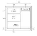
- FIG. 4 is a diagram showing a planar layout of the I/O circuit 10 in the second comparative example.
- the I/O cell 110 and the NC cell 140 are individually arranged as independent standard cells. Referring to the figure, the I/O cell 110 and the NC cell 140 are arranged side by side in the left-right direction in the drawing when the semiconductor device 1 is viewed from above.
- the I/O cell 110 and the NC cell 140 are each independent standard cells.
- PW type well
- the distance between the elements separating the diode D2 and the transistor N4 becomes long, which may hinder the reduction in area of the I/O circuit 10 (and by extension, the semiconductor device 1).
- FIG. 6 is a diagram illustrating a new embodiment of an I/O circuit.
- the I/O circuit 10 of this embodiment is formed by combining multiple types of standard cells included in the I/O cell library 100.
- the I/O circuit 10 of this embodiment includes at least an I/O cell 150 as a plurality of types of standard cells.
- the I/O circuit 10 may include a combination of the previously mentioned VCC cell 120, GND cell 130, and the like.
- the I/O cell 150 includes a first element formation region 151, a second element formation region 152, and a third element formation region 153.
- the first element formation region 151 is arranged immediately (or in the vicinity) of the signal terminal T1 connected to the signal line L1. Note that in the first element formation region 151, a transistor P11 (for example, PMOSFET), a transistor N11 (for example, NMOSFET), and a resistor R11 are formed.
- a transistor P11 for example, PMOSFET
- a transistor N11 for example, NMOSFET
- a resistor R11 are formed in the first element formation region 151.
- the drains of transistors P11 and N11 are both connected to signal line L1.
- the source, gate, and back gate of the transistor P11 are all connected to the power supply line L2.
- the gate of transistor N11 is connected to the first end of resistor R11.
- the source and back gate of the transistor N11 and the second end of the resistor R11 are both connected to the ground line L3. Note that the resistor R11 for pulling down the gate of the transistor N11 may be omitted.
- the transistors P11 and N11 whose gates and sources are short-circuited are connected to the first ESD protection element connected between the signal line L1 and the power line L2, and the first ESD protection element connected between the signal line L1 and the ground line L3, respectively. It functions as a second ESD protection element connected between.
- These first and second ESD protection elements each protect protected elements (in this figure, transistors P12 and N13, which will be described later) connected to the signal line L1 from ESD pulses.
- the transistors P11 and N11 may be replaced with diodes, respectively, as in the first comparative example (FIG. 2) and the second comparative example (FIG. 3).
- the second element formation region 152 is arranged immediately (or in the vicinity) of the first element formation region 151.
- the second element formation region 152 is arranged adjacent to the first element formation region 151.
- the second element formation region 152 is arranged between the signal terminal T1 and the first element formation region 151.
- a transistor N12 for example, NMOSFET
- a resistor R12 are formed in the second element formation region 152.
- the drain of the transistor N12 is connected to the power supply line L2.
- the gate of transistor N12 is connected to the first end of resistor R12.
- the source and back gate of the transistor N12 and the second end of the resistor R12 are both connected to the ground line L3. Note that the resistor R12 for pulling down the gate of the transistor N12 may be omitted.
- the transistor N12 whose gate and source are short-circuited functions as a third ESD protection element connected to the power supply line L2 and the ground line L3. Note that the transistor N12 may be replaced with a diode.
- the second element formation region 152, the first element formation region 151, and the third element formation region 153 are arranged in order from the side closer to the signal terminal T1.
- a transistor P12 for example, PMOSFET
- a transistor N13 for example, NMOSFET
- the source and back gate of the transistor P12 are both connected to the power supply line L2.
- the source and back gate of transistor N13 are both connected to ground line L3.
- the drains of transistors P12 and N13 are both connected to an internal circuit (not shown).
- the gates of transistors P12 and N13 are both connected to signal terminal T1 via signal line L1.
- Transistors P12 and N13 connected in this way form a CMOS inverter (so-called input buffer). Note that an output buffer or an input/output buffer may be formed in the third element formation region 153 instead of the input buffer.
- a current may flow in a current path from the signal terminal T1 to the ground terminal T3 via the signal line L1, the transistor P11, the power supply line L2, the transistor N12, and the ground line L3.
- the I/O circuit 10 of this embodiment even if the distance between the signal terminal T1 and the power supply terminal T2 or the ground terminal T3 is long, the influence of wiring impedance can be suppressed.
- the I/O cell 150 can be understood as a combination of the I/O cell 110 and the NC cell 140 of the second comparative example (FIG. 3) into one standard cell. Therefore, it is not necessary to design the protection element size and arrange the cells in consideration of the wiring impedance. Furthermore, there is no need to worry about the ESD protection function failing due to the circuit designer of the semiconductor device 1 forgetting to place the NC cell 140.
- FIG. 7 is a diagram showing a planar layout of the I/O circuit 10 in this embodiment. As shown in this figure, transistors P11, N11, and N12 (corresponding to the first to third ESD protection elements) are each arranged as one of the components forming a single I/O cell 150. be done.
- the I/O cell 150 can be understood as a combination of the I/O cell 110 and the NC cell 140 of the second comparative example (FIG. 3) into one standard cell.
- the inter-element distance separating the transistor N11 and the transistor N12 is shortened, the area of the I/O circuit 10 (and thus the semiconductor device 1) can be reduced.
- the I/O circuit disclosed in this specification is formed by arbitrarily combining multiple types of standard cells included in a cell library, and the I/O circuit included in the multiple types of standard cells is
- the I/O cell includes a first protection element connected between a signal line and a power line, and a second protection element connected between the signal line and a ground line. a second element formation area configured such that a third protection element connected between the power supply line and the ground line is formed;
- the three protection elements are all formed in a common well (first configuration).
- the I/O circuit according to the first configuration may have a configuration (second configuration) further including a third element formation region configured to form a protected element connected to the signal line. .
- the protected element may be configured to form an input buffer, an output buffer, or an input/output buffer (third configuration).
- the first protection element is a P-channel type first transistor, and the source, gate, and back gate of the first transistor are all connected to the power source.
- a configuration (fourth configuration) may be adopted in which the drain of the first transistor is connected to the signal line and the drain of the first transistor is connected to the signal line.
- the second protection element is an N-channel type second transistor, and the source, gate, and back gate of the second transistor are all directly connected to each other. Alternatively, it may be indirectly connected to the ground line, and the drain of the second transistor may be connected to the signal line (fifth configuration).
- the third protection element is an N-channel type third transistor, and the source, gate, and back gate of the third transistor are all directly connected to each other.
- the third transistor may be indirectly connected to the ground line, and the drain of the third transistor may be connected to the power supply line (sixth configuration).
- the semiconductor device disclosed in this specification includes an I/O circuit having any one of the first to sixth configurations, an external terminal configured to be connected to the signal line, (seventh configuration).
- the I/O cell may be arranged in a region immediately below a pad connected to the external terminal (eighth configuration).
- the cell library disclosed herein includes multiple types that can be read out from a circuit design program executed by a computer and arbitrarily combined to form an I/O circuit of a semiconductor device.
- the I/O cells included in the plurality of types of standard cells include a first protection element connected between a signal line and a power line and a first protection element connected between the signal line and a ground line. a first element formation region configured such that a second protection element connected therebetween is formed; and a third protection element connected between the power supply line and the ground line
- the second protective element and the third protective element are both formed in a common well (a ninth configuration).
- the method for designing a circuit for a semiconductor device disclosed in this specification uses the ninth cell library, and includes selecting and arranging the plurality of types of standard cells included in the cell library. and a step of laying the power supply line, the ground line, and the signal line so as to connect the arbitrarily combined plurality of types of standard cells and other circuit blocks. (10th configuration).
Landscapes
- Design And Manufacture Of Integrated Circuits (AREA)
- Semiconductor Integrated Circuits (AREA)
Priority Applications (1)
| Application Number | Priority Date | Filing Date | Title |
|---|---|---|---|
| JP2024546768A JPWO2024057763A1 (https=) | 2022-09-14 | 2023-08-03 |
Applications Claiming Priority (2)
| Application Number | Priority Date | Filing Date | Title |
|---|---|---|---|
| JP2022145941 | 2022-09-14 | ||
| JP2022-145941 | 2022-09-14 |
Publications (1)
| Publication Number | Publication Date |
|---|---|
| WO2024057763A1 true WO2024057763A1 (ja) | 2024-03-21 |
Family
ID=90274754
Family Applications (1)
| Application Number | Title | Priority Date | Filing Date |
|---|---|---|---|
| PCT/JP2023/028414 Ceased WO2024057763A1 (ja) | 2022-09-14 | 2023-08-03 | I/o回路、半導体装置、セルライブラリ、半導体装置の回路設計方法 |
Country Status (2)
| Country | Link |
|---|---|
| JP (1) | JPWO2024057763A1 (https=) |
| WO (1) | WO2024057763A1 (https=) |
Citations (6)
| Publication number | Priority date | Publication date | Assignee | Title |
|---|---|---|---|---|
| JPH11251453A (ja) * | 1998-12-28 | 1999-09-17 | Seiko Epson Corp | 半導体集積装置 |
| JP2002050698A (ja) * | 2000-08-02 | 2002-02-15 | Nec Corp | 半導体装置 |
| JP2009164195A (ja) * | 2007-12-28 | 2009-07-23 | Panasonic Corp | 半導体チップ |
| JP2009206402A (ja) * | 2008-02-29 | 2009-09-10 | Fujitsu Microelectronics Ltd | 半導体装置の設計方法及び半導体装置 |
| JP2010080622A (ja) * | 2008-09-25 | 2010-04-08 | Panasonic Corp | 半導体集積回路 |
| JP2022105405A (ja) * | 2021-01-04 | 2022-07-14 | ローム株式会社 | 保護回路およびこの保護回路を備える半導体集積回路 |
-
2023
- 2023-08-03 JP JP2024546768A patent/JPWO2024057763A1/ja active Pending
- 2023-08-03 WO PCT/JP2023/028414 patent/WO2024057763A1/ja not_active Ceased
Patent Citations (6)
| Publication number | Priority date | Publication date | Assignee | Title |
|---|---|---|---|---|
| JPH11251453A (ja) * | 1998-12-28 | 1999-09-17 | Seiko Epson Corp | 半導体集積装置 |
| JP2002050698A (ja) * | 2000-08-02 | 2002-02-15 | Nec Corp | 半導体装置 |
| JP2009164195A (ja) * | 2007-12-28 | 2009-07-23 | Panasonic Corp | 半導体チップ |
| JP2009206402A (ja) * | 2008-02-29 | 2009-09-10 | Fujitsu Microelectronics Ltd | 半導体装置の設計方法及び半導体装置 |
| JP2010080622A (ja) * | 2008-09-25 | 2010-04-08 | Panasonic Corp | 半導体集積回路 |
| JP2022105405A (ja) * | 2021-01-04 | 2022-07-14 | ローム株式会社 | 保護回路およびこの保護回路を備える半導体集積回路 |
Also Published As
| Publication number | Publication date |
|---|---|
| JPWO2024057763A1 (https=) | 2024-03-21 |
Similar Documents
| Publication | Publication Date | Title |
|---|---|---|
| US8759883B2 (en) | Semiconductor integrated circuit | |
| JP3990352B2 (ja) | 半導体集積回路装置 | |
| US10748933B2 (en) | Semiconductor device | |
| KR100564979B1 (ko) | 반도체 집적 장치와 그 설계 방법 | |
| KR20130012565A (ko) | 반도체 집적 회로 | |
| JP2009177044A (ja) | 電気ヒューズ回路 | |
| US9430602B2 (en) | Semiconductor integrated circuit device and method for designing layout of the same having standard cells, basic cells and a protective diode cell | |
| US7940113B2 (en) | Fuse trimming circuit with higher reliability | |
| US20050156275A1 (en) | Protection circuit located under fuse window | |
| JP2011015111A (ja) | 入出力インターフェース回路、集積回路装置および電子機器 | |
| CN107112281B (zh) | 半导体装置以及其设计方法 | |
| JP2009147040A (ja) | 半導体集積回路装置 | |
| JP2017037949A (ja) | 半導体装置 | |
| CN104867922B (zh) | 半导体集成电路装置以及使用该装置的电子设备 | |
| JP5002967B2 (ja) | 半導体装置及びその製造方法 | |
| JP2010041013A (ja) | 保護回路 | |
| US7764108B2 (en) | Electrical fuse circuit | |
| WO2024057763A1 (ja) | I/o回路、半導体装置、セルライブラリ、半導体装置の回路設計方法 | |
| US6426650B1 (en) | Integrated circuit with metal programmable logic having enhanced reliability | |
| JP5087897B2 (ja) | 半導体装置 | |
| US20070081282A1 (en) | Electrostatic discharge (esd) protection apparatus for programmable device | |
| KR20030084541A (ko) | 반도체 집적 회로 장치, 실장 기판 장치 및 실장 기판장치의 배선 절단 방법 | |
| JP7644697B2 (ja) | 半導体装置 | |
| US12471388B2 (en) | Semiconductor device | |
| JP2025076038A (ja) | 半導体装置 |
Legal Events
| Date | Code | Title | Description |
|---|---|---|---|
| 121 | Ep: the epo has been informed by wipo that ep was designated in this application |
Ref document number: 23865123 Country of ref document: EP Kind code of ref document: A1 |
|
| WWE | Wipo information: entry into national phase |
Ref document number: 2024546768 Country of ref document: JP |
|
| NENP | Non-entry into the national phase |
Ref country code: DE |
|
| 122 | Ep: pct application non-entry in european phase |
Ref document number: 23865123 Country of ref document: EP Kind code of ref document: A1 |