WO2024057763A1 - I/o circuit, semiconductor device, cell library, and method for designing circuit of semiconductor device - Google Patents
I/o circuit, semiconductor device, cell library, and method for designing circuit of semiconductor device Download PDFInfo
- Publication number
- WO2024057763A1 WO2024057763A1 PCT/JP2023/028414 JP2023028414W WO2024057763A1 WO 2024057763 A1 WO2024057763 A1 WO 2024057763A1 JP 2023028414 W JP2023028414 W JP 2023028414W WO 2024057763 A1 WO2024057763 A1 WO 2024057763A1
- Authority
- WO
- WIPO (PCT)
- Prior art keywords
- circuit
- transistor
- protection element
- cell
- line
- Prior art date
Links
- 239000004065 semiconductor Substances 0.000 title claims description 36
- 238000000034 method Methods 0.000 title claims description 7
- 230000015572 biosynthetic process Effects 0.000 claims abstract description 34
- 230000000052 comparative effect Effects 0.000 description 25
- 238000010586 diagram Methods 0.000 description 18
- 230000006870 function Effects 0.000 description 15
- 230000001681 protective effect Effects 0.000 description 2
- 238000004891 communication Methods 0.000 description 1
- 230000000295 complement effect Effects 0.000 description 1
- 230000005669 field effect Effects 0.000 description 1
- 230000001771 impaired effect Effects 0.000 description 1
- 238000002955 isolation Methods 0.000 description 1
- 229910044991 metal oxide Inorganic materials 0.000 description 1
- 150000004706 metal oxides Chemical class 0.000 description 1
- 238000012986 modification Methods 0.000 description 1
- 230000004048 modification Effects 0.000 description 1
- 230000002093 peripheral effect Effects 0.000 description 1
- 230000009467 reduction Effects 0.000 description 1
- 230000004044 response Effects 0.000 description 1
- 230000003068 static effect Effects 0.000 description 1
Images


Classifications
-
- H—ELECTRICITY
- H01—ELECTRIC ELEMENTS
- H01L—SEMICONDUCTOR DEVICES NOT COVERED BY CLASS H10
- H01L21/00—Processes or apparatus adapted for the manufacture or treatment of semiconductor or solid state devices or of parts thereof
- H01L21/70—Manufacture or treatment of devices consisting of a plurality of solid state components formed in or on a common substrate or of parts thereof; Manufacture of integrated circuit devices or of parts thereof
- H01L21/77—Manufacture or treatment of devices consisting of a plurality of solid state components or integrated circuits formed in, or on, a common substrate
- H01L21/78—Manufacture or treatment of devices consisting of a plurality of solid state components or integrated circuits formed in, or on, a common substrate with subsequent division of the substrate into plural individual devices
- H01L21/82—Manufacture or treatment of devices consisting of a plurality of solid state components or integrated circuits formed in, or on, a common substrate with subsequent division of the substrate into plural individual devices to produce devices, e.g. integrated circuits, each consisting of a plurality of components
- H01L21/822—Manufacture or treatment of devices consisting of a plurality of solid state components or integrated circuits formed in, or on, a common substrate with subsequent division of the substrate into plural individual devices to produce devices, e.g. integrated circuits, each consisting of a plurality of components the substrate being a semiconductor, using silicon technology
- H01L21/8232—Field-effect technology
- H01L21/8234—MIS technology, i.e. integration processes of field effect transistors of the conductor-insulator-semiconductor type
-
- H—ELECTRICITY
- H01—ELECTRIC ELEMENTS
- H01L—SEMICONDUCTOR DEVICES NOT COVERED BY CLASS H10
- H01L27/00—Devices consisting of a plurality of semiconductor or other solid-state components formed in or on a common substrate
- H01L27/02—Devices consisting of a plurality of semiconductor or other solid-state components formed in or on a common substrate including semiconductor components specially adapted for rectifying, oscillating, amplifying or switching and having at least one potential-jump barrier or surface barrier; including integrated passive circuit elements with at least one potential-jump barrier or surface barrier
- H01L27/04—Devices consisting of a plurality of semiconductor or other solid-state components formed in or on a common substrate including semiconductor components specially adapted for rectifying, oscillating, amplifying or switching and having at least one potential-jump barrier or surface barrier; including integrated passive circuit elements with at least one potential-jump barrier or surface barrier the substrate being a semiconductor body
- H01L27/06—Devices consisting of a plurality of semiconductor or other solid-state components formed in or on a common substrate including semiconductor components specially adapted for rectifying, oscillating, amplifying or switching and having at least one potential-jump barrier or surface barrier; including integrated passive circuit elements with at least one potential-jump barrier or surface barrier the substrate being a semiconductor body including a plurality of individual components in a non-repetitive configuration
Definitions
- the invention disclosed herein relates to an I/O [input/output] circuit, a semiconductor device, a cell library, and a circuit design method for a semiconductor device.
- circuit design of a semiconductor device is performed by arbitrarily combining multiple types of standard cells included in a cell library.
- Patent Documents 1 and 2 can be cited as prior art related to the above.
- JP2010-28126A Japanese Patent Application Publication No. 2010-192932
- the I/O circuit disclosed in this specification is formed by arbitrarily combining multiple types of standard cells included in a cell library, and the I/O circuit included in the multiple types of standard cells is
- the I/O cell includes a first protection element connected between a signal line and a power line, and a second protection element connected between the signal line and a ground line. a second element formation area configured such that a third protection element connected between the power supply line and the ground line is formed; All three protection elements are formed in a common well.
- FIG. 1 is a diagram showing an example of the configuration of a semiconductor device.
- FIG. 2 is a diagram showing a first comparative example of an I/O circuit.
- FIG. 3 is a diagram showing a second comparative example of the I/O circuit.
- FIG. 4 is a diagram showing a planar layout of an I/O circuit in a second comparative example.
- FIG. 5 is a diagram showing a vertical cross section of an I/O circuit in a second comparative example.
- FIG. 6 is a diagram illustrating a novel embodiment of an I/O circuit.
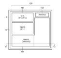
- FIG. 7 is a diagram showing a planar layout of the I/O circuit in the embodiment.
- FIG. 8 is a diagram showing a vertical cross section of the I/O circuit in the embodiment.
- FIG. 1 is a diagram showing an example of the configuration of a semiconductor device.
- the semiconductor device 1 of this configuration example is an LSI [large scale integrated circuit] that integrates a CMOS [complementary metal oxide semiconductor] circuit (logic/analog mixed circuit) that is mainly driven at 5 V or less.
- CMOS complementary metal oxide semiconductor
- I/O circuit 10 having an ESD protection function and a signal input/output function is arranged.
- the semiconductor device 1 includes various internal circuits such as a logic circuit LOGIC, an analog circuit ANALOG, an interface circuit I/F, a nonvolatile memory NVM, and a volatile memory SRAM. , a digital/analog converter DAC, an analog/digital converter ADC, and a regulator LDO are integrated.
- the I/O circuit 10 may be arranged along the four sides of the semiconductor device 1 so as to surround the above-mentioned internal circuit in a plan view of the semiconductor device 1.
- the semiconductor device 1 controls a controller (such as an ECU [electronic control unit]) installed in various terminal devices (such as an LED [light emitting diode] lamp, a motor, or a switch) in response to a command via an in-vehicle network.
- a controller such as an ECU [electronic control unit]
- terminal devices such as an LED [light emitting diode] lamp, a motor, or a switch
- an in-vehicle network such as an LED [light emitting diode] lamp, a motor, or a switch
- IC integrated circuit
- the interface circuit I/F may be compliant with any in-vehicle network (for example, LIN [local interconnect network], CXPI [clock extension peripheral interface], and CAN [controller area network]).
- the I/O circuit 10 of the first comparative example is formed by arbitrarily combining multiple types of standard cells included in the I/O cell library 100.
- the I/O cell library 100 is read from a circuit design program executed by a computer, and can be understood as a type of circuit design database.
- each of the plurality of types of standard cells described above is provided with an interface function (ESD protection function and signal input/output function) with the outside of the device.
- interface function ESD protection function and signal input/output function
- the multiple types of standard cells listed above have their own shapes and layouts so that even if one standard cell is replaced with another standard cell, there is no need to make any modifications to the standard cells placed around it. has been standardized.
- a circuit design method for the semiconductor device 1 (particularly the I/O circuit 10) using the I/O cell library 100 will be briefly described. First, a step of selecting and arranging a plurality of types of standard cells included in the I/O cell library 100 and combining them arbitrarily is carried out. Next, a step of laying power supply lines, signal lines, etc. to connect the arbitrarily combined plural types of standard cells and other circuit blocks is carried out. Finally, a step is performed to verify whether the designed circuit satisfies desired conditions (electrical characteristics, etc.).
- the I/O circuit 10 of this comparative example is formed by combining the I/O cell 110, the VCC cell 120, and the GND cell 130 as the plurality of types of standard cells described above. There is.
- the I/O cell 110 is one of the standard cells arranged in the immediate vicinity of the signal terminal T1 connected to the signal line L1.
- the I/O cell 110 includes a transistor P1 (for example, a PMOSFET [P-channel type MOS field effect transistor]), a transistor N1 (for example, an NMOSFET [N-channel type MOSFET]), and a diode. D1 and D2.
- the source and back gate of the transistor P1 are both connected to the power supply line L2.
- the source and back gate of transistor N1 are both connected to ground line L3.
- the drains of transistors P1 and N1 are both connected to an internal circuit (not shown).
- the gates of transistors P1 and N1 are both connected to signal terminal T1 via signal line L1.
- Transistors P1 and N1 connected in this way form a CMOS inverter (so-called input buffer). Note that an output buffer or an input/output buffer may be formed in the I/O cell 110 instead of the input buffer.
- the anode of the diode D1 and the cathode of the diode D2 are both connected to the signal line L1.
- the cathode of the diode D1 is connected to the power supply line L2.
- the anode of diode D2 is connected to ground line L3.
- the diodes D1 and D2 connected in this manner each function as an ESD protection element for protecting protected elements (transistors P1 and N1 in this figure) each having a gate electrically connected to the signal terminal T1.
- the diodes D1 and D2 may each be a body diode of a transistor whose gate and source are shorted.
- the VCC cell 120 includes a transistor N2 (eg, NMOSFET) and a resistor R2.
- the drain of the transistor N2 is connected to the power supply line L2.
- the gate of transistor N2 is connected to the first end of resistor R2.
- the source and back gate of the transistor N2 and the second end of the resistor R2 are both connected to the ground line L3. Note that the resistor R2 for pulling down the gate of the transistor N2 may be omitted.
- Transistor N2 connected in this manner functions as an ESD protection element between power supply and ground.
- the GND cell 130 includes a transistor N3 (eg, NMOSFET) and a resistor R3.
- the drain of the transistor N3 is connected to the power supply line L2.
- the gate of transistor N3 is connected to the first end of resistor R3.
- the source and back gate of the transistor N3 and the second end of the resistor R3 are both connected to the ground line L3. Note that the resistor R3 for pulling down the gate of the transistor N3 may be omitted.
- the transistor N3 connected in this manner functions as an ESD protection element between the power supply and ground, like the transistor N2 mentioned above.
- the I/O circuit 10 of the first comparative example when the distance between the signal terminal T1 and the power supply terminal T2 or the ground terminal T3 is long, the current path from the I/O cell 110 to the VCC cell 120 and the GND cell 130 is Wiring impedance increases. As a result, there is a possibility that the ESD protection function of the I/O cell 110 will not be achieved.
- FIG. 3 is a diagram showing a second comparative example of the I/O circuit.
- the I/O circuit 10 of the second comparative example is based on the previously mentioned first comparative example (FIG. 2), but in addition to the previously mentioned I/O cell 110, VCC cell 120, and GND cell 130, It further includes an NC [non-connected] cell 140.
- the NC cell 140 is one of the standard cells that is not directly connected to any terminal provided on the semiconductor device 1.
- the NC cell 140 is arranged mainly to fill in the space between a plurality of standard cells. Referring to the figure, the NC cell 140 is placed in the immediate vicinity of the I/O cell 110 (specifically, between the I/O cell 110 and the VCC cell 120).
- NC cell 140 includes a transistor N4 (eg, NMOSFET) and a resistor R4.
- the drain of the transistor N4 is connected to the power supply line L2.
- the gate of transistor N4 is connected to the first end of resistor R4.
- the source and back gate of the transistor N4 and the second end of the resistor R4 are both connected to the ground line L3. Note that the resistor R4 for pulling down the gate of the transistor N4 may be omitted.
- Transistor N4 connected in this manner functions as an ESD protection element between the power supply and ground, like the transistors N2 and N3 described above.
- the NC cell 140 is arranged immediately (or in the vicinity) of the I/O cell 110.
- a current may flow in a current path from the signal terminal T1 to the ground terminal T3 via the signal line L1, the diode D1, the power line L2, the transistor N4, and the ground line L3.
- the I/O circuit 10 of the second comparative example even if the distance between the signal terminal T1 and the power supply terminal T2 or the ground terminal T3 is long, the influence of wiring impedance can be suppressed to a small level. As a result, the ESD protection function of the I/O cell 110 is less likely to be impaired.
- the location where the NC cell 140 is arranged also differs depending on the model. Therefore, it is inevitable that some wiring impedance is attached to the current path for escaping the ESD pulse. Therefore, it is necessary to design the protection element size and arrange the cells in consideration of the wiring impedance.
- the NC cell 140 cannot be placed immediately (or in the vicinity) of the I/O cell 110, the wiring impedance of the above-described current path may increase. As a result, there is a possibility that the ESD protection function of the I/O cell 110 will not be achieved.
- FIG. 4 is a diagram showing a planar layout of the I/O circuit 10 in the second comparative example.
- the I/O cell 110 and the NC cell 140 are individually arranged as independent standard cells. Referring to the figure, the I/O cell 110 and the NC cell 140 are arranged side by side in the left-right direction in the drawing when the semiconductor device 1 is viewed from above.
- the I/O cell 110 and the NC cell 140 are each independent standard cells.
- PW type well
- the distance between the elements separating the diode D2 and the transistor N4 becomes long, which may hinder the reduction in area of the I/O circuit 10 (and by extension, the semiconductor device 1).
- FIG. 6 is a diagram illustrating a new embodiment of an I/O circuit.
- the I/O circuit 10 of this embodiment is formed by combining multiple types of standard cells included in the I/O cell library 100.
- the I/O circuit 10 of this embodiment includes at least an I/O cell 150 as a plurality of types of standard cells.
- the I/O circuit 10 may include a combination of the previously mentioned VCC cell 120, GND cell 130, and the like.
- the I/O cell 150 includes a first element formation region 151, a second element formation region 152, and a third element formation region 153.
- the first element formation region 151 is arranged immediately (or in the vicinity) of the signal terminal T1 connected to the signal line L1. Note that in the first element formation region 151, a transistor P11 (for example, PMOSFET), a transistor N11 (for example, NMOSFET), and a resistor R11 are formed.
- a transistor P11 for example, PMOSFET
- a transistor N11 for example, NMOSFET
- a resistor R11 are formed in the first element formation region 151.
- the drains of transistors P11 and N11 are both connected to signal line L1.
- the source, gate, and back gate of the transistor P11 are all connected to the power supply line L2.
- the gate of transistor N11 is connected to the first end of resistor R11.
- the source and back gate of the transistor N11 and the second end of the resistor R11 are both connected to the ground line L3. Note that the resistor R11 for pulling down the gate of the transistor N11 may be omitted.
- the transistors P11 and N11 whose gates and sources are short-circuited are connected to the first ESD protection element connected between the signal line L1 and the power line L2, and the first ESD protection element connected between the signal line L1 and the ground line L3, respectively. It functions as a second ESD protection element connected between.
- These first and second ESD protection elements each protect protected elements (in this figure, transistors P12 and N13, which will be described later) connected to the signal line L1 from ESD pulses.
- the transistors P11 and N11 may be replaced with diodes, respectively, as in the first comparative example (FIG. 2) and the second comparative example (FIG. 3).
- the second element formation region 152 is arranged immediately (or in the vicinity) of the first element formation region 151.
- the second element formation region 152 is arranged adjacent to the first element formation region 151.
- the second element formation region 152 is arranged between the signal terminal T1 and the first element formation region 151.
- a transistor N12 for example, NMOSFET
- a resistor R12 are formed in the second element formation region 152.
- the drain of the transistor N12 is connected to the power supply line L2.
- the gate of transistor N12 is connected to the first end of resistor R12.
- the source and back gate of the transistor N12 and the second end of the resistor R12 are both connected to the ground line L3. Note that the resistor R12 for pulling down the gate of the transistor N12 may be omitted.
- the transistor N12 whose gate and source are short-circuited functions as a third ESD protection element connected to the power supply line L2 and the ground line L3. Note that the transistor N12 may be replaced with a diode.
- the second element formation region 152, the first element formation region 151, and the third element formation region 153 are arranged in order from the side closer to the signal terminal T1.
- a transistor P12 for example, PMOSFET
- a transistor N13 for example, NMOSFET
- the source and back gate of the transistor P12 are both connected to the power supply line L2.
- the source and back gate of transistor N13 are both connected to ground line L3.
- the drains of transistors P12 and N13 are both connected to an internal circuit (not shown).
- the gates of transistors P12 and N13 are both connected to signal terminal T1 via signal line L1.
- Transistors P12 and N13 connected in this way form a CMOS inverter (so-called input buffer). Note that an output buffer or an input/output buffer may be formed in the third element formation region 153 instead of the input buffer.
- a current may flow in a current path from the signal terminal T1 to the ground terminal T3 via the signal line L1, the transistor P11, the power supply line L2, the transistor N12, and the ground line L3.
- the I/O circuit 10 of this embodiment even if the distance between the signal terminal T1 and the power supply terminal T2 or the ground terminal T3 is long, the influence of wiring impedance can be suppressed.
- the I/O cell 150 can be understood as a combination of the I/O cell 110 and the NC cell 140 of the second comparative example (FIG. 3) into one standard cell. Therefore, it is not necessary to design the protection element size and arrange the cells in consideration of the wiring impedance. Furthermore, there is no need to worry about the ESD protection function failing due to the circuit designer of the semiconductor device 1 forgetting to place the NC cell 140.
- FIG. 7 is a diagram showing a planar layout of the I/O circuit 10 in this embodiment. As shown in this figure, transistors P11, N11, and N12 (corresponding to the first to third ESD protection elements) are each arranged as one of the components forming a single I/O cell 150. be done.
- the I/O cell 150 can be understood as a combination of the I/O cell 110 and the NC cell 140 of the second comparative example (FIG. 3) into one standard cell.
- the inter-element distance separating the transistor N11 and the transistor N12 is shortened, the area of the I/O circuit 10 (and thus the semiconductor device 1) can be reduced.
- the I/O circuit disclosed in this specification is formed by arbitrarily combining multiple types of standard cells included in a cell library, and the I/O circuit included in the multiple types of standard cells is
- the I/O cell includes a first protection element connected between a signal line and a power line, and a second protection element connected between the signal line and a ground line. a second element formation area configured such that a third protection element connected between the power supply line and the ground line is formed;
- the three protection elements are all formed in a common well (first configuration).
- the I/O circuit according to the first configuration may have a configuration (second configuration) further including a third element formation region configured to form a protected element connected to the signal line. .
- the protected element may be configured to form an input buffer, an output buffer, or an input/output buffer (third configuration).
- the first protection element is a P-channel type first transistor, and the source, gate, and back gate of the first transistor are all connected to the power source.
- a configuration (fourth configuration) may be adopted in which the drain of the first transistor is connected to the signal line and the drain of the first transistor is connected to the signal line.
- the second protection element is an N-channel type second transistor, and the source, gate, and back gate of the second transistor are all directly connected to each other. Alternatively, it may be indirectly connected to the ground line, and the drain of the second transistor may be connected to the signal line (fifth configuration).
- the third protection element is an N-channel type third transistor, and the source, gate, and back gate of the third transistor are all directly connected to each other.
- the third transistor may be indirectly connected to the ground line, and the drain of the third transistor may be connected to the power supply line (sixth configuration).
- the semiconductor device disclosed in this specification includes an I/O circuit having any one of the first to sixth configurations, an external terminal configured to be connected to the signal line, (seventh configuration).
- the I/O cell may be arranged in a region immediately below a pad connected to the external terminal (eighth configuration).
- the cell library disclosed herein includes multiple types that can be read out from a circuit design program executed by a computer and arbitrarily combined to form an I/O circuit of a semiconductor device.
- the I/O cells included in the plurality of types of standard cells include a first protection element connected between a signal line and a power line and a first protection element connected between the signal line and a ground line. a first element formation region configured such that a second protection element connected therebetween is formed; and a third protection element connected between the power supply line and the ground line
- the second protective element and the third protective element are both formed in a common well (a ninth configuration).
- the method for designing a circuit for a semiconductor device disclosed in this specification uses the ninth cell library, and includes selecting and arranging the plurality of types of standard cells included in the cell library. and a step of laying the power supply line, the ground line, and the signal line so as to connect the arbitrarily combined plurality of types of standard cells and other circuit blocks. (10th configuration).
Abstract
This I/O circuit 10 is formed by discretionarily combining a plurality of types of standard cells included in a cell library 100. A standard cell 150 included in the plurality of types of standard cells includes: a first element formation region 151 configured such that a first protection element P11 connected between a signal line and a power supply line and a second protection element N11 connected between the signal line and a ground line are formed; and a second element formation region 152 configured such that a third protection element N12 connected between the power supply line and the ground line is formed. Both the second protection element N11 and the third protection element N12 are formed in a common well.
Description
本明細書中に開示されている発明は、I/O[input/output]回路、半導体装置、セルライブラリ、及び、半導体装置の回路設計方法に関する。
The invention disclosed herein relates to an I/O [input/output] circuit, a semiconductor device, a cell library, and a circuit design method for a semiconductor device.
従来、セルライブラリに含まれる複数種類の標準セルを任意に組み合わせることにより半導体装置の回路設計を行う手法が知られている。
Conventionally, a method is known in which circuit design of a semiconductor device is performed by arbitrarily combining multiple types of standard cells included in a cell library.
なお、上記に関連する従来技術としては、特許文献1及び2を挙げることができる。
Note that Patent Documents 1 and 2 can be cited as prior art related to the above.
しかしながら、従来のI/O回路では、信号端子と電源端子又は接地端子との距離が遠いほど信号端子に印加されるESD[electro static discharge]パルスを逃がし難くなってESD耐性の低下を招くおそれがあった。
However, in conventional I/O circuits, the greater the distance between the signal terminal and the power supply terminal or the ground terminal, the more difficult it becomes to escape the ESD [electro static discharge] pulse applied to the signal terminal, which may lead to a decrease in ESD resistance. there were.
例えば、本明細書中に開示されているI/O回路は、セルライブラリに含まれる複数種類の標準セルを任意に組み合わせることにより形成されるものであって、前記複数種類の標準セルに含まれるI/Oセルは、信号線と電源線との間に接続される第1保護素子及び前記信号線と接地線との間に接続される第2保護素子が形成されるように構成された第1素子形成領域と、前記電源線と前記接地線との間に接続される第3保護素子が形成されるように構成された第2素子形成領域と、を含み、前記第2保護素子及び第3保護素子は、いずれも共通のウェルに形成されている。
For example, the I/O circuit disclosed in this specification is formed by arbitrarily combining multiple types of standard cells included in a cell library, and the I/O circuit included in the multiple types of standard cells is The I/O cell includes a first protection element connected between a signal line and a power line, and a second protection element connected between the signal line and a ground line. a second element formation area configured such that a third protection element connected between the power supply line and the ground line is formed; All three protection elements are formed in a common well.
なお、その他の特徴、要素、ステップ、利点、及び、特性については、以下に続く発明を実施するための形態及びこれに関する添付の図面によって、さらに明らかとなる。
Note that other features, elements, steps, advantages, and characteristics will become clearer from the detailed description and accompanying drawings that follow.
本開示によれば、ESD耐性の高いI/O回路を提供することが可能となる。
According to the present disclosure, it is possible to provide an I/O circuit with high ESD resistance.
<半導体装置>
図1は、半導体装置の一構成例を示す図である。本構成例の半導体装置1は、主に5V以下で駆動するCMOS[complementary metal oxide semiconductor]回路(ロジック/アナログ混載回路)を集積化したLSI[large scale integrated circuit]である。半導体装置1の最外周部には、ESD保護機能及び信号入出力機能を担うI/O回路10が配置されている。 <Semiconductor device>
FIG. 1 is a diagram showing an example of the configuration of a semiconductor device. Thesemiconductor device 1 of this configuration example is an LSI [large scale integrated circuit] that integrates a CMOS [complementary metal oxide semiconductor] circuit (logic/analog mixed circuit) that is mainly driven at 5 V or less. At the outermost periphery of the semiconductor device 1, an I/O circuit 10 having an ESD protection function and a signal input/output function is arranged.
図1は、半導体装置の一構成例を示す図である。本構成例の半導体装置1は、主に5V以下で駆動するCMOS[complementary metal oxide semiconductor]回路(ロジック/アナログ混載回路)を集積化したLSI[large scale integrated circuit]である。半導体装置1の最外周部には、ESD保護機能及び信号入出力機能を担うI/O回路10が配置されている。 <Semiconductor device>
FIG. 1 is a diagram showing an example of the configuration of a semiconductor device. The
半導体装置1には、I/O回路10以外にも、種々の内部回路が集積化されている。本図に即して述べると、半導体装置1には、種々の内部回路として、ロジック回路LOGICと、アナログ回路ANALOGと、インタフェイス回路I/Fと、不揮発性メモリNVMと、揮発性メモリSRAMと、デジタル/アナログ変換器DACと、アナログ/デジタル変換器ADCと、レギュレータLDOが集積化されている。
In addition to the I/O circuit 10, various internal circuits are integrated in the semiconductor device 1. Referring to this diagram, the semiconductor device 1 includes various internal circuits such as a logic circuit LOGIC, an analog circuit ANALOG, an interface circuit I/F, a nonvolatile memory NVM, and a volatile memory SRAM. , a digital/analog converter DAC, an analog/digital converter ADC, and a regulator LDO are integrated.
I/O回路10は、半導体装置1の平面視において、上記の内部回路を取り囲むように半導体装置1の四辺に沿って配置してもよい。
The I/O circuit 10 may be arranged along the four sides of the semiconductor device 1 so as to surround the above-mentioned internal circuit in a plan view of the semiconductor device 1.
半導体装置1としては、例えば、車載ネットワーク経由で指令を受けて各種の末端装置(LED[light emitting diode]ランプ、モータ又はスイッチなど)に搭載されたコントローラ(ECU[electronic control unit]など)を制御する車載向けの統合通信IC[integrated circuit]を挙げることができる。この場合、インタフェイス回路I/Fは、任意の車載ネットワーク(例えばLIN[local interconnect network]、CXPI[clock extension peripheral interface]及びCAN[controller area network])に準拠してもよい。
For example, the semiconductor device 1 controls a controller (such as an ECU [electronic control unit]) installed in various terminal devices (such as an LED [light emitting diode] lamp, a motor, or a switch) in response to a command via an in-vehicle network. One example is an integrated communication IC [integrated circuit] for in-vehicle use. In this case, the interface circuit I/F may be compliant with any in-vehicle network (for example, LIN [local interconnect network], CXPI [clock extension peripheral interface], and CAN [controller area network]).
<I/O回路(第1比較例)>
図2は、I/O回路の第1比較例(=後出の実施形態と対比される一般的な構成例)を示す図である。第1比較例のI/O回路10は、I/Oセルライブラリ100に含まれる複数種類の標準セルを任意に組み合わせることにより形成されている。I/Oセルライブラリ100は、コンピュータで実行される回路設計プログラムから読み出されるものであり、回路設計用データベースの一種として理解することができる。 <I/O circuit (first comparative example)>
FIG. 2 is a diagram showing a first comparative example of an I/O circuit (=a general configuration example to be compared with the embodiment described later). The I/O circuit 10 of the first comparative example is formed by arbitrarily combining multiple types of standard cells included in the I/O cell library 100. The I/O cell library 100 is read from a circuit design program executed by a computer, and can be understood as a type of circuit design database.
図2は、I/O回路の第1比較例(=後出の実施形態と対比される一般的な構成例)を示す図である。第1比較例のI/O回路10は、I/Oセルライブラリ100に含まれる複数種類の標準セルを任意に組み合わせることにより形成されている。I/Oセルライブラリ100は、コンピュータで実行される回路設計プログラムから読み出されるものであり、回路設計用データベースの一種として理解することができる。 <I/O circuit (first comparative example)>
FIG. 2 is a diagram showing a first comparative example of an I/O circuit (=a general configuration example to be compared with the embodiment described later). The I/
なお、上記複数種類の標準セルは、それぞれ、装置外部とのインタフェイス機能(ESD保護機能及び信号入出力機能)を備えている。また、上記複数種類の標準セルは、いずれかの標準セルを別の標準セルに置換しても、その周囲に配置された標準セルに一切修正を加える必要がないように、それぞれの形状及びレイアウトが規格化されている。
Note that each of the plurality of types of standard cells described above is provided with an interface function (ESD protection function and signal input/output function) with the outside of the device. In addition, the multiple types of standard cells listed above have their own shapes and layouts so that even if one standard cell is replaced with another standard cell, there is no need to make any modifications to the standard cells placed around it. has been standardized.
I/Oセルライブラリ100を用いた半導体装置1(特にI/O回路10)の回路設計方法について簡単に説明しておく。まず、I/Oセルライブラリ100に含まれる複数種類の標準セルを選択及び配置して任意に組み合わせるステップを実施する。次に、任意に組み合わされた複数種類の標準セルとその他の回路ブロックとを接続するように電源線及び信号線などを敷設するステップを実施する。最後に、設計済み回路が所望の条件(電気的特性など)を満足しているか否かを検証するステップを実施する。
A circuit design method for the semiconductor device 1 (particularly the I/O circuit 10) using the I/O cell library 100 will be briefly described. First, a step of selecting and arranging a plurality of types of standard cells included in the I/O cell library 100 and combining them arbitrarily is carried out. Next, a step of laying power supply lines, signal lines, etc. to connect the arbitrarily combined plural types of standard cells and other circuit blocks is carried out. Finally, a step is performed to verify whether the designed circuit satisfies desired conditions (electrical characteristics, etc.).
このようなI/Oセルライブラリ100を用いて半導体装置1(特にI/O回路10)の回路設計を行うことにより、ESD耐性、ラッチアップ耐性及び電気的特性などを端子毎に設計する必要がなくなる。従って、回路設計者の負担を減らすとともに設計ミスを減らすことができる。
By designing the circuit of the semiconductor device 1 (particularly the I/O circuit 10) using such an I/O cell library 100, it is no longer necessary to design ESD resistance, latch-up resistance, electrical characteristics, etc. for each terminal. It disappears. Therefore, it is possible to reduce the burden on the circuit designer and reduce design errors.
なお、本図に即して述べると、本比較例のI/O回路10は、上記した複数種類の標準セルとしてI/Oセル110、VCCセル120及びGNDセル130を組み合わせることにより形成されている。
Note that, referring to this figure, the I/O circuit 10 of this comparative example is formed by combining the I/O cell 110, the VCC cell 120, and the GND cell 130 as the plurality of types of standard cells described above. There is.
I/Oセル110は、信号線L1に接続される信号端子T1の直近に配置される標準セルの一つである。本図に即して述べると、I/Oセル110は、トランジスタP1(例えばPMOSFET[P-channel type MOS field effect transistor])と、トランジスタN1(例えばNMOSFET[N-channel type MOSFET])と、ダイオードD1及びD2と、を含む。
The I/O cell 110 is one of the standard cells arranged in the immediate vicinity of the signal terminal T1 connected to the signal line L1. Referring to this diagram, the I/O cell 110 includes a transistor P1 (for example, a PMOSFET [P-channel type MOS field effect transistor]), a transistor N1 (for example, an NMOSFET [N-channel type MOSFET]), and a diode. D1 and D2.
トランジスタP1のソースとバックゲートは、いずれも電源線L2に接続されている。トランジスタN1のソースとバックゲートは、いずれも接地線L3に接続されている。トランジスタP1及びN1それぞれのドレインは、いずれも不図示の内部回路に接続されている。トランジスタP1及びN1それぞれのゲートは、いずれも信号線L1を介して信号端子T1に接続されている。このように接続されたトランジスタP1及びN1は、CMOSインバータ(いわゆる入力バッファ)を形成する。なお、I/Oセル110には、入力バッファに代えて出力バッファ又は入出力バッファが形成されてもよい。
The source and back gate of the transistor P1 are both connected to the power supply line L2. The source and back gate of transistor N1 are both connected to ground line L3. The drains of transistors P1 and N1 are both connected to an internal circuit (not shown). The gates of transistors P1 and N1 are both connected to signal terminal T1 via signal line L1. Transistors P1 and N1 connected in this way form a CMOS inverter (so-called input buffer). Note that an output buffer or an input/output buffer may be formed in the I/O cell 110 instead of the input buffer.
ダイオードD1のアノードとダイオードD2のカソードは、いずれも信号線L1に接続されている。ダイオードD1のカソードは、電源線L2に接続されている。ダイオードD2のアノードは、接地線L3に接続されている。このように接続されたダイオードD1及びD2は、それぞれ、信号端子T1と導通するゲートを備えた被保護素子(本図ではトランジスタP1及びN1)を保護するためのESD保護素子として機能する。なお、ダイオードD1及びD2は、それぞれ、ゲート・ソース間がショートされたトランジスタのボディダイオードであってもよい。
The anode of the diode D1 and the cathode of the diode D2 are both connected to the signal line L1. The cathode of the diode D1 is connected to the power supply line L2. The anode of diode D2 is connected to ground line L3. The diodes D1 and D2 connected in this manner each function as an ESD protection element for protecting protected elements (transistors P1 and N1 in this figure) each having a gate electrically connected to the signal terminal T1. Note that the diodes D1 and D2 may each be a body diode of a transistor whose gate and source are shorted.
VCCセル120は、電源線L2に接続される電源端子T2(=電源電圧VCCの印加端)の直近に配置される標準セルの一つ(いわゆる電源保護セル)である。本図に即して述べると、VCCセル120は、トランジスタN2(例えばNMOSFET)と、抵抗R2と、を含む。
The VCC cell 120 is one of the standard cells (so-called power protection cell) that is placed in the immediate vicinity of the power supply terminal T2 (=the end to which power supply voltage VCC is applied) connected to the power supply line L2. Referring to this figure, the VCC cell 120 includes a transistor N2 (eg, NMOSFET) and a resistor R2.
トランジスタN2のドレインは、電源線L2に接続されている。トランジスタN2のゲートは、抵抗R2の第1端に接続されている。トランジスタN2のソース及びバックゲートと抵抗R2の第2端は、いずれも接地線L3に接続されている。なお、トランジスタN2のゲートをプルダウンするための抵抗R2は、省略され得る。このように接続されたトランジスタN2は、電源/接地間のESD保護素子として機能する。
The drain of the transistor N2 is connected to the power supply line L2. The gate of transistor N2 is connected to the first end of resistor R2. The source and back gate of the transistor N2 and the second end of the resistor R2 are both connected to the ground line L3. Note that the resistor R2 for pulling down the gate of the transistor N2 may be omitted. Transistor N2 connected in this manner functions as an ESD protection element between power supply and ground.
GNDセル130は、接地線L3に接続される接地端子T3(=接地電圧GNDの印加端)の直近に配置される標準セルの一つ(いわゆるGND保護セル)である。本図に即して述べると、GNDセル130は、トランジスタN3(例えばNMOSFET)と、抵抗R3と、を含む。
The GND cell 130 is one of the standard cells (so-called GND protection cell) placed in the immediate vicinity of the ground terminal T3 (=the end to which the ground voltage GND is applied) connected to the ground line L3. Referring to this figure, the GND cell 130 includes a transistor N3 (eg, NMOSFET) and a resistor R3.
トランジスタN3のドレインは、電源線L2に接続されている。トランジスタN3のゲートは、抵抗R3の第1端に接続されている。トランジスタN3のソース及びバックゲートと抵抗R3の第2端は、いずれも接地線L3に接続されている。なお、トランジスタN3のゲートをプルダウンするための抵抗R3は、省略され得る。このように接続されたトランジスタN3は、先出のトランジスタN2と同じく、電源/接地間のESD保護素子として機能する。
The drain of the transistor N3 is connected to the power supply line L2. The gate of transistor N3 is connected to the first end of resistor R3. The source and back gate of the transistor N3 and the second end of the resistor R3 are both connected to the ground line L3. Note that the resistor R3 for pulling down the gate of the transistor N3 may be omitted. The transistor N3 connected in this manner functions as an ESD protection element between the power supply and ground, like the transistor N2 mentioned above.
例えば、信号端子T1に印加されるESDパルスを接地端子T3に逃がしてESD保護を掛ける場合を考える。この場合、図示の細い矢印で示したように、信号端子T1から信号線L1、ダイオードD1、電源線L2、トランジスタN2又はN3、及び、接地線L3を介して接地端子T3に至る電流経路に電流が流れ得る。
For example, consider a case where ESD protection is applied by letting the ESD pulse applied to the signal terminal T1 escape to the ground terminal T3. In this case, as shown by the thin arrow in the figure, a current flows through the current path from the signal terminal T1 to the ground terminal T3 via the signal line L1, the diode D1, the power line L2, the transistor N2 or N3, and the ground line L3. can flow.
しかし、第1比較例のI/O回路10では、信号端子T1と電源端子T2又は接地端子T3との距離が遠い場合、I/Oセル110からVCCセル120及びGNDセル130に至る電流経路の配線インピーダンスが大きくなる。その結果、I/Oセル110のESD保護機能が成立しなくなるおそれがある。
However, in the I/O circuit 10 of the first comparative example, when the distance between the signal terminal T1 and the power supply terminal T2 or the ground terminal T3 is long, the current path from the I/O cell 110 to the VCC cell 120 and the GND cell 130 is Wiring impedance increases. As a result, there is a possibility that the ESD protection function of the I/O cell 110 will not be achieved.
<I/O回路(第2比較例)>
図3は、I/O回路の第2比較例を示す図である。第2比較例のI/O回路10は、先出の第1比較例(図2)を基本としつつ、先出のI/Oセル110、VCCセル120、及び、GNDセル130に加えて、NC[non-connected]セル140をさらに含む。 <I/O circuit (second comparative example)>
FIG. 3 is a diagram showing a second comparative example of the I/O circuit. The I/O circuit 10 of the second comparative example is based on the previously mentioned first comparative example (FIG. 2), but in addition to the previously mentioned I/O cell 110, VCC cell 120, and GND cell 130, It further includes an NC [non-connected] cell 140.
図3は、I/O回路の第2比較例を示す図である。第2比較例のI/O回路10は、先出の第1比較例(図2)を基本としつつ、先出のI/Oセル110、VCCセル120、及び、GNDセル130に加えて、NC[non-connected]セル140をさらに含む。 <I/O circuit (second comparative example)>
FIG. 3 is a diagram showing a second comparative example of the I/O circuit. The I/
NCセル140は、その名の通り、半導体装置1に設けられるいずれの端子にも直接繋がることのない標準セルの一つである。NCセル140は、主に複数の標準セルの間を埋めるように配置される。本図に即して述べると、NCセル140は、I/Oセル110の直近(具体的にはI/Oセル110とVCCセル120との間)に配置されている。NCセル140は、トランジスタN4(例えばNMOSFET)と、抵抗R4と、を含む。
As its name suggests, the NC cell 140 is one of the standard cells that is not directly connected to any terminal provided on the semiconductor device 1. The NC cell 140 is arranged mainly to fill in the space between a plurality of standard cells. Referring to the figure, the NC cell 140 is placed in the immediate vicinity of the I/O cell 110 (specifically, between the I/O cell 110 and the VCC cell 120). NC cell 140 includes a transistor N4 (eg, NMOSFET) and a resistor R4.
トランジスタN4のドレインは、電源線L2に接続されている。トランジスタN4のゲートは、抵抗R4の第1端に接続されている。トランジスタN4のソース及びバックゲートと抵抗R4の第2端は、いずれも接地線L3に接続されている。なお、トランジスタN4のゲートをプルダウンするための抵抗R4は、省略され得る。このように接続されたトランジスタN4は、先出のトランジスタN2及びN3と同様、電源/接地間のESD保護素子として機能する。
The drain of the transistor N4 is connected to the power supply line L2. The gate of transistor N4 is connected to the first end of resistor R4. The source and back gate of the transistor N4 and the second end of the resistor R4 are both connected to the ground line L3. Note that the resistor R4 for pulling down the gate of the transistor N4 may be omitted. Transistor N4 connected in this manner functions as an ESD protection element between the power supply and ground, like the transistors N2 and N3 described above.
このように、第2比較例のI/O回路10では、I/Oセル110の直近(又は近傍)にNCセル140が配置されている。
In this way, in the I/O circuit 10 of the second comparative example, the NC cell 140 is arranged immediately (or in the vicinity) of the I/O cell 110.
例えば、信号端子T1に印加されるESDパルスを接地端子T3に逃がしてESD保護を掛ける場合を考える。この場合、図示の細い矢印で示したように、信号端子T1から信号線L1、ダイオードD1、電源線L2、トランジスタN4及び接地線L3を介して接地端子T3に至る電流経路に電流が流れ得る。
For example, consider a case where ESD protection is applied by letting the ESD pulse applied to the signal terminal T1 escape to the ground terminal T3. In this case, as indicated by the thin arrow in the figure, a current may flow in a current path from the signal terminal T1 to the ground terminal T3 via the signal line L1, the diode D1, the power line L2, the transistor N4, and the ground line L3.
従って、第2比較例のI/O回路10であれば、信号端子T1と電源端子T2又は接地端子T3との距離が遠くても、配線インピーダンスの影響を小さく抑えることができる。その結果、I/Oセル110のESD保護機能に支障を来し難くなる。
Therefore, with the I/O circuit 10 of the second comparative example, even if the distance between the signal terminal T1 and the power supply terminal T2 or the ground terminal T3 is long, the influence of wiring impedance can be suppressed to a small level. As a result, the ESD protection function of the I/O cell 110 is less likely to be impaired.
ただし、端子間の距離は機種毎に異なるので、NCセル140が配置される場所も機種毎に異なる。そのため、ESDパルスを逃がすための電流経路に多少の配線インピーダンスが付随することは避けられない。そのため、配線インピーダンスを考慮した保護素子サイズの設計及びセル配置が必要となる。
However, since the distance between the terminals differs depending on the model, the location where the NC cell 140 is arranged also differs depending on the model. Therefore, it is inevitable that some wiring impedance is attached to the current path for escaping the ESD pulse. Therefore, it is necessary to design the protection element size and arrange the cells in consideration of the wiring impedance.
また、NCセル140をI/Oセル110の直近(又は近傍)に配置することができない場合には、上記した電流経路の配線インピーダンスが増大し得る。その結果、I/Oセル110のESD保護機能が成立しなくなるおそれがある。
Furthermore, if the NC cell 140 cannot be placed immediately (or in the vicinity) of the I/O cell 110, the wiring impedance of the above-described current path may increase. As a result, there is a possibility that the ESD protection function of the I/O cell 110 will not be achieved.
また、半導体装置1の回路設計者がNCセル140を配置し忘れるおそれもある。
Additionally, there is a risk that the circuit designer of the semiconductor device 1 may forget to place the NC cell 140.
図4は、第2比較例におけるI/O回路10の平面レイアウトを示す図である。第2比較例におけるI/O回路10では、I/Oセル110とNCセル140がそれぞれ独立した標準セルとして個別に配置される。本図に即して述べると、I/Oセル110とNCセル140は、半導体装置1の平面視において、紙面左右方向に並べて配置されている。
FIG. 4 is a diagram showing a planar layout of the I/O circuit 10 in the second comparative example. In the I/O circuit 10 in the second comparative example, the I/O cell 110 and the NC cell 140 are individually arranged as independent standard cells. Referring to the figure, the I/O cell 110 and the NC cell 140 are arranged side by side in the left-right direction in the drawing when the semiconductor device 1 is viewed from above.
図5は、第2比較例におけるI/O回路10の縦断面(=図4のX1-X2断面)を示す図である。先にも述べたように、I/Oセル110とNCセル140は、それぞれ独立した標準セルである。
FIG. 5 is a diagram showing a vertical cross section (=X1-X2 cross section in FIG. 4) of the I/O circuit 10 in the second comparative example. As mentioned above, the I/O cell 110 and the NC cell 140 are each independent standard cells.
そのため、I/Oセル110に含まれるダイオードD2(例えばゲート・ソース間がショートされたNMOSFETのボディダイオード)と、NCセル140に含まれるトランジスタN4は、それぞれ、電位的に分離された個別のP型ウェル(PW)に形成される。すなわち、ダイオードD2(=ゲート・ソース間がショートされたNMOSFETのボディダイオード)とトランジスタN4それぞれのバックゲートは、互いに分離されている。
Therefore, the diode D2 (for example, the body diode of an NMOSFET whose gate and source are shorted) included in the I/O cell 110 and the transistor N4 included in the NC cell 140 are each potential-separated individual PMOSFETs. It is formed in a type well (PW). That is, the diode D2 (=the body diode of the NMOSFET whose gate and source are shorted) and the back gates of the transistors N4 are separated from each other.
従って、ダイオードD2とトランジスタN4との間を隔てる素子間距離が長くなり、I/O回路10(延いては半導体装置1)の小面積化が阻害され得る。
Therefore, the distance between the elements separating the diode D2 and the transistor N4 becomes long, which may hinder the reduction in area of the I/O circuit 10 (and by extension, the semiconductor device 1).
そこで、以下では、ESD耐圧向上と小面積化を両立することのできる新規な実施形態を提案する。
Therefore, below, we will propose a new embodiment that can both improve the ESD withstand voltage and reduce the area.
<I/O回路(実施形態)>
図6はI/O回路の新規な実施形態を示す図である。本実施形態のI/O回路10は、I/Oセルライブラリ100に含まれる複数種類の標準セルを組み合わせることにより形成されている。特に、本実施形態のI/O回路10は、複数種類の標準セルとして、少なくともI/Oセル150を含む。なお、本図では明示されていないが、I/O回路10では、先出のVCCセル120及びGNDセル130などが組み合わされていてもよい。 <I/O circuit (embodiment)>
FIG. 6 is a diagram illustrating a new embodiment of an I/O circuit. The I/O circuit 10 of this embodiment is formed by combining multiple types of standard cells included in the I/O cell library 100. In particular, the I/O circuit 10 of this embodiment includes at least an I/O cell 150 as a plurality of types of standard cells. Although not clearly shown in this figure, the I/O circuit 10 may include a combination of the previously mentioned VCC cell 120, GND cell 130, and the like.
図6はI/O回路の新規な実施形態を示す図である。本実施形態のI/O回路10は、I/Oセルライブラリ100に含まれる複数種類の標準セルを組み合わせることにより形成されている。特に、本実施形態のI/O回路10は、複数種類の標準セルとして、少なくともI/Oセル150を含む。なお、本図では明示されていないが、I/O回路10では、先出のVCCセル120及びGNDセル130などが組み合わされていてもよい。 <I/O circuit (embodiment)>
FIG. 6 is a diagram illustrating a new embodiment of an I/O circuit. The I/
I/Oセル150は、第1素子形成領域151と、第2素子形成領域152と、第3素子形成領域153と、を含む。
The I/O cell 150 includes a first element formation region 151, a second element formation region 152, and a third element formation region 153.
第1素子形成領域151は、信号線L1に接続される信号端子T1の直近(又は近傍)に配置されている。なお、第1素子形成領域151には、トランジスタP11(例えばPMOSFET)と、トランジスタN11(例えばNMOSFET)と、抵抗R11が形成されている。
The first element formation region 151 is arranged immediately (or in the vicinity) of the signal terminal T1 connected to the signal line L1. Note that in the first element formation region 151, a transistor P11 (for example, PMOSFET), a transistor N11 (for example, NMOSFET), and a resistor R11 are formed.
トランジスタP11及びN11それぞれのドレインは、いずれも信号線L1に接続されている。トランジスタP11のソース、ゲート及びバックゲートは、いずれも電源線L2に接続されている。トランジスタN11のゲートは、抵抗R11の第1端に接続されている。トランジスタN11のソース及びバックゲートと抵抗R11の第2端は、いずれも接地線L3に接続されている。なお、トランジスタN11のゲートをプルダウンするための抵抗R11は、省略され得る。
The drains of transistors P11 and N11 are both connected to signal line L1. The source, gate, and back gate of the transistor P11 are all connected to the power supply line L2. The gate of transistor N11 is connected to the first end of resistor R11. The source and back gate of the transistor N11 and the second end of the resistor R11 are both connected to the ground line L3. Note that the resistor R11 for pulling down the gate of the transistor N11 may be omitted.
このように、ゲート・ソース間がショートされたトランジスタP11及びN11は、それぞれ、信号線L1と電源線L2との間に接続される第1のESD保護素子、及び、信号線L1と接地線L3との間に接続される第2のESD保護素子として機能する。これら第1及び第2のESD保護素子は、それぞれ、信号線L1に接続される被保護素子(本図では、後出のトランジスタP12及びN13)をESDパルスから保護する。なお、トランジスタP11及びN11は、それぞれ、第1比較例(図2)及び第2比較例(図3)に倣い、ダイオードに置き換えられてもよい。
In this way, the transistors P11 and N11 whose gates and sources are short-circuited are connected to the first ESD protection element connected between the signal line L1 and the power line L2, and the first ESD protection element connected between the signal line L1 and the ground line L3, respectively. It functions as a second ESD protection element connected between. These first and second ESD protection elements each protect protected elements (in this figure, transistors P12 and N13, which will be described later) connected to the signal line L1 from ESD pulses. Note that the transistors P11 and N11 may be replaced with diodes, respectively, as in the first comparative example (FIG. 2) and the second comparative example (FIG. 3).
第2素子形成領域152は、第1素子形成領域151の直近(又は近傍)に配置されている。好ましくは、第2素子形成領域152が第1素子形成領域151に隣接して配置されるとよい。本図に即して述べると、第2素子形成領域152は、信号端子T1と第1素子形成領域151との間に配置されている。なお、第2素子形成領域152には、トランジスタN12(例えばNMOSFET)と、抵抗R12が形成されている。
The second element formation region 152 is arranged immediately (or in the vicinity) of the first element formation region 151. Preferably, the second element formation region 152 is arranged adjacent to the first element formation region 151. Referring to this figure, the second element formation region 152 is arranged between the signal terminal T1 and the first element formation region 151. Note that a transistor N12 (for example, NMOSFET) and a resistor R12 are formed in the second element formation region 152.
トランジスタN12のドレインは、電源線L2に接続されている。トランジスタN12のゲートは、抵抗R12の第1端に接続されている。トランジスタN12のソース及びバックゲートと抵抗R12の第2端は、いずれも接地線L3に接続されている。なお、トランジスタN12のゲートをプルダウンするための抵抗R12は、省略され得る。
The drain of the transistor N12 is connected to the power supply line L2. The gate of transistor N12 is connected to the first end of resistor R12. The source and back gate of the transistor N12 and the second end of the resistor R12 are both connected to the ground line L3. Note that the resistor R12 for pulling down the gate of the transistor N12 may be omitted.
このように、ゲート・ソース間がショートされたトランジスタN12は、電源線L2と接地線L3との接続される第3のESD保護素子として機能する。なお、トランジスタN12は、ダイオードに置き換えられてもよい。
In this way, the transistor N12 whose gate and source are short-circuited functions as a third ESD protection element connected to the power supply line L2 and the ground line L3. Note that the transistor N12 may be replaced with a diode.
第3素子形成領域153は、例えば、第1素子形成領域151及び第2素子形成領域152よりも半導体装置1の内部寄り(=コア側)に配置されている。本図に即して述べると、半導体装置1の平面視において、信号端子T1に近い側から順に、第2素子形成領域152、第1素子形成領域151及び第3素子形成領域153が配置されている。なお、第3素子形成領域153には、トランジスタP12(例えばPMOSFET)と、トランジスタN13(例えばNMOSFET)が形成されている。
The third element formation region 153 is, for example, arranged closer to the inside (=core side) of the semiconductor device 1 than the first element formation region 151 and the second element formation region 152. Referring to this figure, in a plan view of the semiconductor device 1, the second element formation region 152, the first element formation region 151, and the third element formation region 153 are arranged in order from the side closer to the signal terminal T1. There is. Note that a transistor P12 (for example, PMOSFET) and a transistor N13 (for example, NMOSFET) are formed in the third element formation region 153.
トランジスタP12のソース及びバックゲートは、いずれも電源線L2に接続されている。トランジスタN13のソース及びバックゲートは、いずれも接地線L3に接続されている。トランジスタP12及びN13それぞれのドレインは、いずれも不図示の内部回路に接続されている。トランジスタP12及びN13それぞれのゲートは、いずれも信号線L1を介して信号端子T1に接続されている。このように接続されたトランジスタP12及びN13は、CMOSインバータ(いわゆる入力バッファ)を形成する。なお、第3素子形成領域153には、入力バッファに代えて出力バッファ又は入出力バッファが形成されてもよい。
The source and back gate of the transistor P12 are both connected to the power supply line L2. The source and back gate of transistor N13 are both connected to ground line L3. The drains of transistors P12 and N13 are both connected to an internal circuit (not shown). The gates of transistors P12 and N13 are both connected to signal terminal T1 via signal line L1. Transistors P12 and N13 connected in this way form a CMOS inverter (so-called input buffer). Note that an output buffer or an input/output buffer may be formed in the third element formation region 153 instead of the input buffer.
例えば、信号端子T1に印加されるESDパルスを接地端子T3に逃がしてESD保護を掛ける場合を考える。この場合、図示の細い矢印で示したように、信号端子T1から信号線L1、トランジスタP11、電源線L2、トランジスタN12及び接地線L3を介して接地端子T3に至る電流経路に電流が流れ得る。
For example, consider a case where ESD protection is applied by letting the ESD pulse applied to the signal terminal T1 escape to the ground terminal T3. In this case, as indicated by the thin arrow in the figure, a current may flow in a current path from the signal terminal T1 to the ground terminal T3 via the signal line L1, the transistor P11, the power supply line L2, the transistor N12, and the ground line L3.
従って、本実施形態のI/O回路10であれば、信号端子T1と電源端子T2又は接地端子T3との距離が遠くても、配線インピーダンスの影響を小さく抑えることができる。
Therefore, with the I/O circuit 10 of this embodiment, even if the distance between the signal terminal T1 and the power supply terminal T2 or the ground terminal T3 is long, the influence of wiring impedance can be suppressed.
また、I/Oセル150は、第2比較例(図3)のI/Oセル110及びNCセル140を一つの標準セルに集約したものとして理解され得る。従って、配線インピーダンスを考慮した保護素子サイズの設計及びセル配置が不要となる。また、半導体装置1の回路設計者がNCセル140を配置し忘れてESD保護機能が不成立となる心配もなくなる。
Further, the I/O cell 150 can be understood as a combination of the I/O cell 110 and the NC cell 140 of the second comparative example (FIG. 3) into one standard cell. Therefore, it is not necessary to design the protection element size and arrange the cells in consideration of the wiring impedance. Furthermore, there is no need to worry about the ESD protection function failing due to the circuit designer of the semiconductor device 1 forgetting to place the NC cell 140.
図7は、本実施形態におけるI/O回路10の平面レイアウトを示す図である。本図で示したように、トランジスタP11、N11及びN12(それぞれ第1~第3のESD保護素子に相当)は、それぞれ、単一のI/Oセル150を形成する構成要素の一つとして配置される。
FIG. 7 is a diagram showing a planar layout of the I/O circuit 10 in this embodiment. As shown in this figure, transistors P11, N11, and N12 (corresponding to the first to third ESD protection elements) are each arranged as one of the components forming a single I/O cell 150. be done.
特に、先出の第2比較例(図4)と対比すると、トランジスタN11(=第2のESD保護素子)とトランジスタN12(=第3のESD保護素子)とを隔てる素子分離領域が存在しないことが分かる。
In particular, in comparison with the second comparative example (FIG. 4) mentioned above, there is no element isolation region separating transistor N11 (=second ESD protection element) and transistor N12 (=third ESD protection element). I understand.
図8は、本実施形態におけるI/O回路10の縦断面(=図7のY1-Y2断面)を示す図である。先にも述べたように、I/Oセル150は、第2比較例(図3)のI/Oセル110及びNCセル140を一つの標準セルに集約したものとして理解され得る。
FIG. 8 is a diagram showing a vertical cross section (=Y1-Y2 cross section in FIG. 7) of the I/O circuit 10 in this embodiment. As mentioned above, the I/O cell 150 can be understood as a combination of the I/O cell 110 and the NC cell 140 of the second comparative example (FIG. 3) into one standard cell.
そのため、トランジスタN11(=第2のESD保護素子)とトランジスタN12(=第3のESD保護素子)は、それぞれ、共通のP型ウェル(PW)に形成される。すなわち、トランジスタN11及びN12それぞれのバックゲートは、共通化されている。
Therefore, the transistor N11 (=second ESD protection element) and the transistor N12 (=third ESD protection element) are each formed in a common P-type well (PW). That is, the back gates of transistors N11 and N12 are shared.
従って、トランジスタN11とトランジスタN12との間を隔てる素子間距離が短くなるので、I/O回路10(延いては半導体装置1)の小面積化を実現することができる。
Therefore, since the inter-element distance separating the transistor N11 and the transistor N12 is shortened, the area of the I/O circuit 10 (and thus the semiconductor device 1) can be reduced.
なお、I/Oセル150は、第1比較例(図2)及び第2比較例(図3)のI/Oセル110と比べて、トランジスタN12(=第3のESD保護素子)を含む分だけ面積が大きくなる。ただし、このような面積の増大を考慮しても、I/Oセル150は、信号端子T1に接続されるパッドと同程度のサイズに収まる。従って、I/Oセル150は、上記パッドの直下領域に配置されるとよい。このようなレイアウトによれば、I/Oセル150の面積が増大してもインパクトは小さくなる。
Note that the I/O cell 150 is different from the I/O cell 110 of the first comparative example (FIG. 2) and the second comparative example (FIG. 3) in that it includes the transistor N12 (=third ESD protection element). area becomes larger. However, even in consideration of such an increase in area, the I/O cell 150 is still approximately the same size as the pad connected to the signal terminal T1. Therefore, the I/O cell 150 is preferably placed directly under the pad. According to such a layout, even if the area of the I/O cell 150 increases, the impact is small.
<総括>
以下では、上記で説明した種々の実施形態について総括的に述べる。 <Summary>
Below, the various embodiments described above will be described in general.
以下では、上記で説明した種々の実施形態について総括的に述べる。 <Summary>
Below, the various embodiments described above will be described in general.
例えば、本明細書中に開示されているI/O回路は、セルライブラリに含まれる複数種類の標準セルを任意に組み合わせることにより形成されるものであって、前記複数種類の標準セルに含まれるI/Oセルは、信号線と電源線との間に接続される第1保護素子及び前記信号線と接地線との間に接続される第2保護素子が形成されるように構成された第1素子形成領域と、前記電源線と前記接地線との間に接続される第3保護素子が形成されるように構成された第2素子形成領域と、を含み、前記第2保護素子及び第3保護素子は、いずれも共通のウェルに形成されている構成(第1の構成)とされている。
For example, the I/O circuit disclosed in this specification is formed by arbitrarily combining multiple types of standard cells included in a cell library, and the I/O circuit included in the multiple types of standard cells is The I/O cell includes a first protection element connected between a signal line and a power line, and a second protection element connected between the signal line and a ground line. a second element formation area configured such that a third protection element connected between the power supply line and the ground line is formed; The three protection elements are all formed in a common well (first configuration).
上記第1の構成によるI/O回路は、前記信号線に接続される被保護素子が形成されるように構成された第3素子形成領域をさらに含む構成(第2の構成)にしてもよい。
The I/O circuit according to the first configuration may have a configuration (second configuration) further including a third element formation region configured to form a protected element connected to the signal line. .
上記第2の構成によるI/O回路において、前記被保護素子は、入力バッファ、出力バッファ又は入出力バッファを形成する構成(第3の構成)にしてもよい。
In the I/O circuit according to the second configuration, the protected element may be configured to form an input buffer, an output buffer, or an input/output buffer (third configuration).
上記第1~第3いずれかの構成によるI/O回路において、前記第1保護素子は、Pチャネル型の第1トランジスタであり、前記第1トランジスタのソース、ゲート及びバックゲートがいずれも前記電源線に接続されており、前記第1トランジスタのドレインが前記信号線に接続されている構成(第4の構成)にしてもよい。
In the I/O circuit according to any one of the first to third configurations, the first protection element is a P-channel type first transistor, and the source, gate, and back gate of the first transistor are all connected to the power source. A configuration (fourth configuration) may be adopted in which the drain of the first transistor is connected to the signal line and the drain of the first transistor is connected to the signal line.
上記第1~第4いずれかの構成によるI/O回路において、前記第2保護素子は、Nチャネル型の第2トランジスタであり、前記第2トランジスタのソース、ゲート及びバックゲートがいずれも直接的又は間接的に前記接地線に接続されており、前記第2トランジスタのドレインが前記信号線に接続されている構成(第5の構成)にしてもよい。
In the I/O circuit according to any one of the first to fourth configurations, the second protection element is an N-channel type second transistor, and the source, gate, and back gate of the second transistor are all directly connected to each other. Alternatively, it may be indirectly connected to the ground line, and the drain of the second transistor may be connected to the signal line (fifth configuration).
上記第1~第5いずれかの構成によるI/O回路において、前記第3保護素子は、Nチャネル型の第3トランジスタであり、前記第3トランジスタのソース、ゲート及びバックゲートがいずれも直接的又は間接的に前記接地線に接続されており、前記第3トランジスタのドレインが前記電源線に接続されている構成(第6の構成)にしてもよい。
In the I/O circuit according to any one of the first to fifth configurations, the third protection element is an N-channel type third transistor, and the source, gate, and back gate of the third transistor are all directly connected to each other. Alternatively, the third transistor may be indirectly connected to the ground line, and the drain of the third transistor may be connected to the power supply line (sixth configuration).
また、例えば、本明細書中に開示されている半導体装置は、上記第1~第6いずれかの構成によるI/O回路と、前記信号線に接続されるように構成された外部端子と、を備える構成(第7の構成)とされている。
Further, for example, the semiconductor device disclosed in this specification includes an I/O circuit having any one of the first to sixth configurations, an external terminal configured to be connected to the signal line, (seventh configuration).
上記第7の構成による半導体装置において、前記I/Oセルは、前記外部端子に接続されるパッドの直下領域に配置される構成(第8の構成)にしてもよい。
In the semiconductor device according to the seventh configuration, the I/O cell may be arranged in a region immediately below a pad connected to the external terminal (eighth configuration).
また、例えば、本明細書中に開示されているセルライブラリは、コンピュータで実行される回路設計プログラムから読み出されて半導体装置のI/O回路を形成するために任意に組み合わせることのできる複数種類の標準セルを含むものであって、前記複数種類の標準セルに含まれるI/Oセルは、信号線と電源線との間に接続される第1保護素子及び前記信号線と接地線との間に接続される第2保護素子が形成されるように構成された第1素子形成領域と、前記電源線と前記接地線との間に接続される第3保護素子が形成されるように構成された第2素子形成領域と、を含み、前記第2保護素子及び第3保護素子は、いずれも共通のウェルに形成されている構成(第9の構成)とされている。
Furthermore, for example, the cell library disclosed herein includes multiple types that can be read out from a circuit design program executed by a computer and arbitrarily combined to form an I/O circuit of a semiconductor device. The I/O cells included in the plurality of types of standard cells include a first protection element connected between a signal line and a power line and a first protection element connected between the signal line and a ground line. a first element formation region configured such that a second protection element connected therebetween is formed; and a third protection element connected between the power supply line and the ground line The second protective element and the third protective element are both formed in a common well (a ninth configuration).
また、例えば、本明細書中に開示されている半導体装置の回路設計方法は、上記第9のセルライブラリを用いるものであって、前記セルライブラリに含まれる前記複数種類の標準セルを選択及び配置して任意に組み合わせるステップと、任意に組み合わされた前記複数種類の標準セルとその他の回路ブロックとを接続するように前記電源線、前記接地線及び前記信号線を敷設するステップと、を備える構成(第10の構成)とされている。
Further, for example, the method for designing a circuit for a semiconductor device disclosed in this specification uses the ninth cell library, and includes selecting and arranging the plurality of types of standard cells included in the cell library. and a step of laying the power supply line, the ground line, and the signal line so as to connect the arbitrarily combined plurality of types of standard cells and other circuit blocks. (10th configuration).
<その他の変形例>
なお、本明細書中に開示されている種々の技術的特徴は、上記実施形態のほか、その技術的創作の主旨を逸脱しない範囲で種々の変更を加えることが可能である。すなわち、上記実施形態は、全ての点で例示であって制限的なものではないと考えられるべきであり、本開示の技術的範囲は、特許請求の範囲により規定されるものであって、特許請求の範囲と均等の意味及び範囲内に属する全ての変更が含まれると理解されるべきである。 <Other variations>
Note that the various technical features disclosed in this specification can be modified in addition to the above-described embodiments without departing from the gist of the technical creation. In other words, the above embodiments should be considered to be illustrative in all respects and not restrictive, and the technical scope of the present disclosure is defined by the claims, and the technical scope of the present disclosure is defined by the claims. It should be understood that all changes that come within the meaning and range of equivalence of the claims are included.
1 半導体装置
10 I/O回路
100 セルライブラリ
110 I/Oセル
120 VCCセル
130 GNDセル
140 NCセル
150 I/Oセル
151 第1素子形成領域
152 第2素子形成領域
153 第3素子形成領域
ADC アナログ/デジタル変換器
ANALOG アナログ回路
D1、D2 ダイオード
DAC デジタル/アナログ変換器
I/F インタフェイス回路
L1 信号線
L2 電源線
L3 接地線
LDO レギュレータ
LOGIC ロジック回路
N1~N4、N11~N13 トランジスタ(NMOSFET)
NVM 不揮発性メモリ
P1、P11、P12 トランジスタ(PMOSFET)
R2~R4、R11、R12 抵抗
SRAM 揮発性メモリ
T1 信号端子
T2 電源端子
T3 接地端子 1 Semiconductor device 10 I/O circuit 100 Cell library 110 I/O cell 120 VCC cell 130 GND cell 140 NC cell 150 I/O cell 151 First element formation area 152 Second element formation area 153 Third element formation area ADC Analog /Digital converter ANALOG Analog circuit D1, D2 Diode DAC Digital/analog converter I/F Interface circuit L1 Signal line L2 Power line L3 Ground line LDO Regulator LOGIC Logic circuit N1 to N4, N11 to N13 Transistor (NMOSFET)
NVM Non-volatile memory P1, P11, P12 Transistor (PMOSFET)
R2~R4, R11, R12 Resistor SRAM Volatile memory T1 Signal terminal T2 Power supply terminal T3 Ground terminal
10 I/O回路
100 セルライブラリ
110 I/Oセル
120 VCCセル
130 GNDセル
140 NCセル
150 I/Oセル
151 第1素子形成領域
152 第2素子形成領域
153 第3素子形成領域
ADC アナログ/デジタル変換器
ANALOG アナログ回路
D1、D2 ダイオード
DAC デジタル/アナログ変換器
I/F インタフェイス回路
L1 信号線
L2 電源線
L3 接地線
LDO レギュレータ
LOGIC ロジック回路
N1~N4、N11~N13 トランジスタ(NMOSFET)
NVM 不揮発性メモリ
P1、P11、P12 トランジスタ(PMOSFET)
R2~R4、R11、R12 抵抗
SRAM 揮発性メモリ
T1 信号端子
T2 電源端子
T3 接地端子 1 Semiconductor device 10 I/
NVM Non-volatile memory P1, P11, P12 Transistor (PMOSFET)
R2~R4, R11, R12 Resistor SRAM Volatile memory T1 Signal terminal T2 Power supply terminal T3 Ground terminal
Claims (10)
- セルライブラリに含まれる複数種類の標準セルを任意に組み合わせることにより形成されたI/O回路であって、
前記複数種類の標準セルに含まれるI/Oセルは、
信号線と電源線との間に接続される第1保護素子及び前記信号線と接地線との間に接続される第2保護素子が形成されるように構成された第1素子形成領域と、
前記電源線と前記接地線との間に接続される第3保護素子が形成されるように構成された第2素子形成領域と、
を含み、
前記第2保護素子及び前記第3保護素子は、いずれも共通のウェルに形成されている、I/O回路。 An I/O circuit formed by arbitrarily combining multiple types of standard cells included in a cell library,
The I/O cells included in the plurality of types of standard cells are:
a first element formation region configured to form a first protection element connected between the signal line and the power line and a second protection element connected between the signal line and the ground line;
a second element formation region configured to form a third protection element connected between the power supply line and the ground line;
including;
The second protection element and the third protection element are both formed in a common well. - 前記信号線に接続される被保護素子が形成されるように構成された第3素子形成領域をさらに含む、請求項1に記載のI/O回路。 The I/O circuit according to claim 1, further comprising a third element formation region configured such that a protected element connected to the signal line is formed.
- 前記被保護素子は、入力バッファ、出力バッファ又は入出力バッファを形成する、請求項2に記載のI/O回路。 The I/O circuit according to claim 2, wherein the protected element forms an input buffer, an output buffer, or an input/output buffer.
- 前記第1保護素子は、Pチャネル型の第1トランジスタであり、前記第1トランジスタのソース、ゲート及びバックゲートがいずれも前記電源線に接続されており、前記第1トランジスタのドレインが前記信号線に接続されている、請求項1~3のいずれか一項に記載のI/O回路。 The first protection element is a P-channel type first transistor, the source, gate, and back gate of the first transistor are all connected to the power supply line, and the drain of the first transistor is connected to the signal line. The I/O circuit according to any one of claims 1 to 3, which is connected to the I/O circuit.
- 前記第2保護素子は、Nチャネル型の第2トランジスタであり、前記第2トランジスタのソース、ゲート及びバックゲートがいずれも直接的又は間接的に前記接地線に接続されており、前記第2トランジスタのドレインが前記信号線に接続されている、請求項1~4のいずれか一項に記載のI/O回路。 The second protection element is an N-channel type second transistor, and the source, gate, and back gate of the second transistor are all directly or indirectly connected to the ground line, and the second transistor 5. The I/O circuit according to claim 1, wherein a drain of the I/O circuit is connected to the signal line.
- 前記第3保護素子は、Nチャネル型の第3トランジスタであり、前記第3トランジスタのソース、ゲート及びバックゲートがいずれも直接的又は間接的に前記接地線に接続されており、前記第3トランジスタのドレインが前記電源線に接続されている、請求項1~5のいずれか一項に記載のI/O回路。 The third protection element is an N-channel type third transistor, and the source, gate, and back gate of the third transistor are all directly or indirectly connected to the ground line, and the third transistor The I/O circuit according to claim 1, wherein a drain of the I/O circuit is connected to the power supply line.
- 請求項1~6のいずれか一項に記載のI/O回路と、
前記信号線に接続されるように構成された外部端子と、
を備える、半導体装置。 The I/O circuit according to any one of claims 1 to 6,
an external terminal configured to be connected to the signal line;
A semiconductor device comprising: - 前記I/Oセルは、前記外部端子に接続されるパッドの直下領域に配置される、請求項7に記載の半導体装置。 8. The semiconductor device according to claim 7, wherein the I/O cell is arranged in a region directly below a pad connected to the external terminal.
- コンピュータで実行される回路設計プログラムから読み出されて半導体装置のI/O回路を形成するために任意に組み合わせることのできる複数種類の標準セルを含むセルライブラリであって、
前記複数種類の標準セルに含まれるI/Oセルは、
信号線と電源線との間に接続される第1保護素子及び前記信号線と接地線との間に接続される第2保護素子が形成されるように構成された第1素子形成領域と、
前記電源線と前記接地線との間に接続される第3保護素子が形成されるように構成された第2素子形成領域と、
を含み、
前記第2保護素子及び前記第3保護素子は、いずれも共通のウェルに形成されている、セルライブラリ。 A cell library including a plurality of types of standard cells that can be read from a circuit design program executed by a computer and arbitrarily combined to form an I/O circuit of a semiconductor device,
The I/O cells included in the plurality of types of standard cells are:
a first element formation region configured to form a first protection element connected between the signal line and the power line and a second protection element connected between the signal line and the ground line;
a second element formation region configured to form a third protection element connected between the power supply line and the ground line;
including;
The second protection element and the third protection element are both formed in a common well. - 請求項9のセルライブラリを用いた半導体装置の回路設計方法であって、
前記セルライブラリに含まれる前記複数種類の標準セルを選択及び配置して任意に組み合わせるステップと、
任意に組み合わされた前記複数種類の標準セルとその他の回路ブロックとを接続するように前記電源線、前記接地線及び前記信号線を敷設するステップと、
を備える、半導体装置の回路設計方法。 A circuit design method for a semiconductor device using the cell library according to claim 9,
selecting and arranging the plurality of types of standard cells included in the cell library and combining them arbitrarily;
laying the power supply line, the ground line, and the signal line so as to connect the plurality of types of standard cells arbitrarily combined with other circuit blocks;
A circuit design method for a semiconductor device, comprising:
Applications Claiming Priority (2)
| Application Number | Priority Date | Filing Date | Title |
|---|---|---|---|
| JP2022145941 | 2022-09-14 | ||
| JP2022-145941 | 2022-09-14 |
Publications (1)
| Publication Number | Publication Date |
|---|---|
| WO2024057763A1 true WO2024057763A1 (en) | 2024-03-21 |
Family
ID=90274754
Family Applications (1)
| Application Number | Title | Priority Date | Filing Date |
|---|---|---|---|
| PCT/JP2023/028414 WO2024057763A1 (en) | 2022-09-14 | 2023-08-03 | I/o circuit, semiconductor device, cell library, and method for designing circuit of semiconductor device |
Country Status (1)
| Country | Link |
|---|---|
| WO (1) | WO2024057763A1 (en) |
Citations (6)
| Publication number | Priority date | Publication date | Assignee | Title |
|---|---|---|---|---|
| JPH11251453A (en) * | 1998-12-28 | 1999-09-17 | Seiko Epson Corp | Semiconductor integrate device |
| JP2002050698A (en) * | 2000-08-02 | 2002-02-15 | Nec Corp | Semiconductor device |
| JP2009164195A (en) * | 2007-12-28 | 2009-07-23 | Panasonic Corp | Semiconductor chip |
| JP2009206402A (en) * | 2008-02-29 | 2009-09-10 | Fujitsu Microelectronics Ltd | Method for designing semiconductor device, and semiconductor device |
| JP2010080622A (en) * | 2008-09-25 | 2010-04-08 | Panasonic Corp | Semiconductor integrated circuit |
| JP2022105405A (en) * | 2021-01-04 | 2022-07-14 | ローム株式会社 | Protection circuit and semiconductor integrated circuit having protection circuit |
-
2023
- 2023-08-03 WO PCT/JP2023/028414 patent/WO2024057763A1/en unknown
Patent Citations (6)
| Publication number | Priority date | Publication date | Assignee | Title |
|---|---|---|---|---|
| JPH11251453A (en) * | 1998-12-28 | 1999-09-17 | Seiko Epson Corp | Semiconductor integrate device |
| JP2002050698A (en) * | 2000-08-02 | 2002-02-15 | Nec Corp | Semiconductor device |
| JP2009164195A (en) * | 2007-12-28 | 2009-07-23 | Panasonic Corp | Semiconductor chip |
| JP2009206402A (en) * | 2008-02-29 | 2009-09-10 | Fujitsu Microelectronics Ltd | Method for designing semiconductor device, and semiconductor device |
| JP2010080622A (en) * | 2008-09-25 | 2010-04-08 | Panasonic Corp | Semiconductor integrated circuit |
| JP2022105405A (en) * | 2021-01-04 | 2022-07-14 | ローム株式会社 | Protection circuit and semiconductor integrated circuit having protection circuit |
Similar Documents
| Publication | Publication Date | Title |
|---|---|---|
| US8759883B2 (en) | Semiconductor integrated circuit | |
| US7459350B2 (en) | Method for fabricating a protection circuit located under fuse window | |
| KR100564979B1 (en) | Semiconductor integrated device and method for designing the same | |
| JP3990352B2 (en) | Semiconductor integrated circuit device | |
| US8525552B2 (en) | Semiconductor integrated circuit device having a plurality of standard cells for leakage current suppression | |
| KR20130012565A (en) | Semiconductor integrated circuit | |
| JP2009177044A (en) | Electrical fuse circuit | |
| JP5002967B2 (en) | Semiconductor device and manufacturing method thereof | |
| JP5359614B2 (en) | I / O interface circuit, integrated circuit device, and electronic equipment | |
| JP5165356B2 (en) | Semiconductor integrated circuit device | |
| US9430602B2 (en) | Semiconductor integrated circuit device and method for designing layout of the same having standard cells, basic cells and a protective diode cell | |
| US10748933B2 (en) | Semiconductor device | |
| JP2014207413A (en) | Semiconductor device | |
| JP6512520B2 (en) | Semiconductor device and design method thereof | |
| JP5087897B2 (en) | Semiconductor device | |
| WO2024057763A1 (en) | I/o circuit, semiconductor device, cell library, and method for designing circuit of semiconductor device | |
| US20070081282A1 (en) | Electrostatic discharge (esd) protection apparatus for programmable device | |
| KR20010029848A (en) | Semiconductor device | |
| KR100523504B1 (en) | Semiconductor integrated circuit device, mounting substrate apparatus and wire cutting method thereof | |
| CN113764410B (en) | Semiconductor unit device | |
| JP2011096889A (en) | Semiconductor device | |
| WO2023210631A1 (en) | I/o circuit, semiconductor device, cell library, and method for designing circuit of semiconductor device | |
| US20110025378A1 (en) | Semiconductor integrated circuit and layout method thereof | |
| US20230135511A1 (en) | Semiconductor device | |
| JP2007027401A (en) | Semiconductor device |