WO2024057752A1 - 半導体モジュール、半導体装置、及び車両 - Google Patents
半導体モジュール、半導体装置、及び車両 Download PDFInfo
- Publication number
- WO2024057752A1 WO2024057752A1 PCT/JP2023/028240 JP2023028240W WO2024057752A1 WO 2024057752 A1 WO2024057752 A1 WO 2024057752A1 JP 2023028240 W JP2023028240 W JP 2023028240W WO 2024057752 A1 WO2024057752 A1 WO 2024057752A1
- Authority
- WO
- WIPO (PCT)
- Prior art keywords
- section
- partition
- case
- circuit board
- semiconductor module
- Prior art date
- Legal status (The legal status is an assumption and is not a legal conclusion. Google has not performed a legal analysis and makes no representation as to the accuracy of the status listed.)
- Ceased
Links
Images









Classifications
-
- H—ELECTRICITY
- H05—ELECTRIC TECHNIQUES NOT OTHERWISE PROVIDED FOR
- H05K—PRINTED CIRCUITS; CASINGS OR CONSTRUCTIONAL DETAILS OF ELECTRIC APPARATUS; MANUFACTURE OF ASSEMBLAGES OF ELECTRICAL COMPONENTS
- H05K5/00—Casings, cabinets or drawers for electric apparatus
- H05K5/0026—Casings, cabinets or drawers for electric apparatus provided with connectors and printed circuit boards [PCB], e.g. automotive electronic control units
- H05K5/0073—Casings, cabinets or drawers for electric apparatus provided with connectors and printed circuit boards [PCB], e.g. automotive electronic control units having specific features for mounting the housing on an external structure
-
- H—ELECTRICITY
- H10—SEMICONDUCTOR DEVICES; ELECTRIC SOLID-STATE DEVICES NOT OTHERWISE PROVIDED FOR
- H10W—GENERIC PACKAGES, INTERCONNECTIONS, CONNECTORS OR OTHER CONSTRUCTIONAL DETAILS OF DEVICES COVERED BY CLASS H10
- H10W90/00—Package configurations
-
- H—ELECTRICITY
- H05—ELECTRIC TECHNIQUES NOT OTHERWISE PROVIDED FOR
- H05K—PRINTED CIRCUITS; CASINGS OR CONSTRUCTIONAL DETAILS OF ELECTRIC APPARATUS; MANUFACTURE OF ASSEMBLAGES OF ELECTRICAL COMPONENTS
- H05K5/00—Casings, cabinets or drawers for electric apparatus
- H05K5/0026—Casings, cabinets or drawers for electric apparatus provided with connectors and printed circuit boards [PCB], e.g. automotive electronic control units
- H05K5/0047—Casings, cabinets or drawers for electric apparatus provided with connectors and printed circuit boards [PCB], e.g. automotive electronic control units having a two-part housing enclosing a PCB
- H05K5/006—Casings, cabinets or drawers for electric apparatus provided with connectors and printed circuit boards [PCB], e.g. automotive electronic control units having a two-part housing enclosing a PCB characterized by features for holding the PCB within the housing
-
- H—ELECTRICITY
- H05—ELECTRIC TECHNIQUES NOT OTHERWISE PROVIDED FOR
- H05K—PRINTED CIRCUITS; CASINGS OR CONSTRUCTIONAL DETAILS OF ELECTRIC APPARATUS; MANUFACTURE OF ASSEMBLAGES OF ELECTRICAL COMPONENTS
- H05K5/00—Casings, cabinets or drawers for electric apparatus
- H05K5/0091—Housing specially adapted for small components
- H05K5/0095—Housing specially adapted for small components hermetically-sealed
-
- H—ELECTRICITY
- H10—SEMICONDUCTOR DEVICES; ELECTRIC SOLID-STATE DEVICES NOT OTHERWISE PROVIDED FOR
- H10W—GENERIC PACKAGES, INTERCONNECTIONS, CONNECTORS OR OTHER CONSTRUCTIONAL DETAILS OF DEVICES COVERED BY CLASS H10
- H10W70/00—Package substrates; Interposers; Redistribution layers [RDL]
- H10W70/60—Insulating or insulated package substrates; Interposers; Redistribution layers
- H10W70/62—Insulating or insulated package substrates; Interposers; Redistribution layers characterised by their interconnections
- H10W70/65—Shapes or dispositions of interconnections
- H10W70/658—Shapes or dispositions of interconnections for devices provided for in groups H10D8/00 - H10D48/00
-
- H—ELECTRICITY
- H10—SEMICONDUCTOR DEVICES; ELECTRIC SOLID-STATE DEVICES NOT OTHERWISE PROVIDED FOR
- H10W—GENERIC PACKAGES, INTERCONNECTIONS, CONNECTORS OR OTHER CONSTRUCTIONAL DETAILS OF DEVICES COVERED BY CLASS H10
- H10W76/00—Containers; Fillings or auxiliary members therefor; Seals
- H10W76/10—Containers or parts thereof
- H10W76/12—Containers or parts thereof characterised by their shape
- H10W76/15—Containers comprising an insulating or insulated base
-
- H—ELECTRICITY
- H10—SEMICONDUCTOR DEVICES; ELECTRIC SOLID-STATE DEVICES NOT OTHERWISE PROVIDED FOR
- H10W—GENERIC PACKAGES, INTERCONNECTIONS, CONNECTORS OR OTHER CONSTRUCTIONAL DETAILS OF DEVICES COVERED BY CLASS H10
- H10W76/00—Containers; Fillings or auxiliary members therefor; Seals
- H10W76/60—Seals
-
- H—ELECTRICITY
- H02—GENERATION; CONVERSION OR DISTRIBUTION OF ELECTRIC POWER
- H02M—APPARATUS FOR CONVERSION BETWEEN AC AND AC, BETWEEN AC AND DC, OR BETWEEN DC AND DC, AND FOR USE WITH MAINS OR SIMILAR POWER SUPPLY SYSTEMS; CONVERSION OF DC OR AC INPUT POWER INTO SURGE OUTPUT POWER; CONTROL OR REGULATION THEREOF
- H02M7/00—Conversion of AC power input into DC power output; Conversion of DC power input into AC power output
- H02M7/003—Constructional details, e.g. physical layout, assembly, wiring or busbar connections
-
- H—ELECTRICITY
- H10—SEMICONDUCTOR DEVICES; ELECTRIC SOLID-STATE DEVICES NOT OTHERWISE PROVIDED FOR
- H10W—GENERIC PACKAGES, INTERCONNECTIONS, CONNECTORS OR OTHER CONSTRUCTIONAL DETAILS OF DEVICES COVERED BY CLASS H10
- H10W90/00—Package configurations
- H10W90/701—Package configurations characterised by the relative positions of pads or connectors relative to package parts
Definitions
- the present invention relates to a semiconductor module, a semiconductor device, and a vehicle.
- IGBT Insulated Gate Bipolar Transistor
- power MOSFET Metal Oxide Semiconductor Field Effect T
- FWD Free Wheeling Diode
- a circuit board in which circuit components such as semiconductor elements are mounted on a wiring board is housed in a case, and then a sealing material is filled in the case to seal the circuit board.
- Patent Document 1 describes a power circuit module in which a power circuit board on which a power semiconductor is mounted is sealed with an insulating resin with lead terminals pulled out to the outside, and a power circuit module in which a power circuit board on which a power semiconductor is mounted is sealed with an insulating resin, and a state in which a connection part is exposed to the outside. and a control circuit module in which a control circuit board for driving and controlling the power semiconductor is embedded in an insulating resin, and the lead terminals of the power circuit module are attached to the connection parts of the control circuit module to connect electrically.
- a power conversion device is described that is connected to and mechanically integrated with.
- Patent Document 2 describes a semiconductor device in which an epoxy resin is further filled on the upper surface side of a silicone gel that seals a power device and a control circuit in a case.
- the semiconductor module case described above has a side wall that surrounds circuit components such as semiconductor elements mounted on a circuit board, and a lid that serves as a lid above the circuit board. Some have an injection hole for injecting the material. When using such a case, after placing the case over the circuit board, a sealing material is injected through the injection hole to seal the circuit components of the circuit board.
- the circuit is protected by protruding parts such as partitions and beams provided on the surface of the case on the side of the space where the circuit components are housed, and by the sealing material injected from the injection hole.
- Some devices divide a space for accommodating components into two or more spaces to ensure insulation between terminals.
- additional encapsulation is required, for example, to prevent corrosion by corrosive gases. It is difficult to uniformly fill each divided space by injecting the material through the injection hole.
- the present invention aims to reduce uneven filling of encapsulant in a semiconductor module using a case with an integrated lid.
- a semiconductor module includes a base on which a circuit board is mounted, and a case that covers the circuit board mounted on the base, and a side surface surrounding the outer periphery of the circuit board and a case above the circuit board.
- a plurality of conductor plates each electrically connected to a conductor pattern of the circuit board and extending to the outside of the case through a slit provided in the case;
- a sealing material for sealing the circuit board, and the case is disposed in a region surrounded by the lid part, the side part, and the circuit board, and is disposed between the plurality of conductor plates.
- the partition part has a partition part that insulates between the plurality of conductor plates, and the partition part has a partition part that insulates between the plurality of conductor plates, and the partition part has a partition part that insulates between the plurality of conductor plates.
- FIG. 1 is a plan view for explaining a configuration example of a semiconductor device according to an embodiment.
- FIG. 2 is a plan view of the semiconductor device of FIG. 1 with a case omitted;
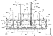
- FIG. 2 is a side cross-sectional view illustrating an example of the configuration of the semiconductor device when viewed from the positive side in the Y direction from the position of line A-A' in FIG. 1;
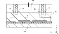
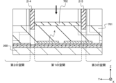
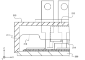
- FIG. 2 is a side sectional view illustrating a configuration example of a semiconductor module when viewed from the position of line B-B' in FIG. 1 on the positive side in the X direction.
- 5 is an enlarged view of region R in FIG. 4.
- FIG. FIG. 2 is a side cross-sectional view for explaining an example of the configuration around the lid of a case in a completed semiconductor device.
- FIG. 2 is an equivalent circuit diagram for one phase in the semiconductor device of FIG. 1.
- FIG. FIG. 3 is a side cross-sectional view of a step of injecting a first sealing material in the manufacturing process of the semiconductor module according to the present embodiment.
- FIG. 7 is a side cross-sectional view of a step of injecting a second sealing material in the manufacturing process of the semiconductor module according to the present embodiment.
- FIG. 7 is a diagram schematically showing the flow of the second sealing material in the step of injecting the second sealing material.
- FIG. 7 is a side cross-sectional view of a step of injecting a first sealing material in a manufacturing process of a semiconductor module in which a partition portion does not have a cutout section.
- FIG. 7 is a side cross-sectional view of a step of injecting a second sealing material in the manufacturing process of a semiconductor module in which the partition portion does not have a cutout section. It is a perspective view explaining the 1st modification of the notch section provided in a partition part. It is a side sectional view explaining the 2nd modification of the notch section provided in a partition part. It is a perspective view explaining the 3rd modification of the notch section provided in a partition part. It is a perspective view explaining the 4th modification of the notch section provided in a partition part.
- FIG. 1 is a schematic plan view showing an example of a vehicle to which a semiconductor device according to the present invention is applied.
- semiconductor module refers to a circuit board on which circuit components such as semiconductor elements are mounted on a wiring board, which is housed in a case, and then the case is filled with a sealing material to remove the circuit board.
- sealing material refers to a sealed device.
- semiconductor device in this specification and claims refers to a device that includes at least one semiconductor module and a component different from the semiconductor module (for example, a cooler, etc.) and is integrated with the components.
- the X direction, Y direction, and Z direction shown in the reference drawings correspond to the longitudinal direction, lateral direction, and height direction of the semiconductor module, respectively.
- the illustrated X, Y, and Z axes are orthogonal to each other and form a right-handed system.
- the Z direction may be referred to as the vertical direction.
- a plan view means a case where the top surface or bottom surface of the semiconductor module is viewed from the Z direction.
- the semiconductor module exemplified in the following description may be applied to a power conversion device such as an inverter device for an industrial or vehicle-mounted motor, for example.
- a power conversion device such as an inverter device for an industrial or vehicle-mounted motor, for example.
- the configuration of the semiconductor module shown in the drawings referred to in the following description is simplified to the extent that it does not hinder the understanding of the present invention by those skilled in the art, and does not necessarily match the configuration of an actual semiconductor module.
- the aspect ratio and the size relationship between each member in each drawing are only schematically or schematically represented, and do not necessarily match the relationship in an actual semiconductor module. For convenience of explanation, it is assumed that the size relationship between each member may be exaggerated.
- detailed descriptions of well-known configurations, functions, operations, manufacturing methods, etc. of semiconductor modules will be omitted to the extent that it does not hinder the understanding of the present invention by those skilled in the art.
- FIG. 1 is a plan view for explaining a configuration example of a semiconductor device according to an embodiment.
- FIG. 2 is a plan view of the semiconductor device shown in FIG. 1 with the case omitted.
- FIG. 3 is a side cross-sectional view illustrating an example of the configuration of the semiconductor device when viewed from the positive side in the Y direction from the position of line A-A' in FIG.
- FIG. 4 is a side sectional view illustrating a configuration example of a semiconductor module when viewed from the position of line B-B' in FIG. 1 on the positive side in the X direction.
- FIG. 5 is an enlarged view of region R in FIG.
- FIG. 6 is a side cross-sectional view for explaining an example of the structure around the lid of the case in a completed semiconductor device.
- FIG. 1 is a plan view for explaining a configuration example of a semiconductor device according to an embodiment.
- FIG. 2 is a plan view of the semiconductor device shown in FIG. 1 with the case omitted.
- FIGS. 1 to 5 show a state in which a semiconductor module in the semiconductor device according to the present embodiment is being manufactured, more specifically, a state in which a case is attached to a base on which a circuit board is mounted; The state before the sealing material is injected into the interior is illustrated.
- the semiconductor device 1 illustrated in FIGS. 1 to 5 includes a semiconductor module 2 and a cooler 3 disposed on the lower surface of the semiconductor module 2.
- the cooler 3 radiates heat from the semiconductor module 2 to the outside, and has a rectangular parallelepiped shape as a whole.
- the cooler 3 is configured by providing a plurality of fins on the lower surface side of the base portion and housing these fins in a water jacket. Note that the configuration of the cooler 3 is not limited to this and can be changed as appropriate.
- the semiconductor module 2 is electrically connected to a base 200 on which a circuit board 4 and the like are mounted, a case 210 that covers the circuit board 4 and the like mounted on the base 200, and a conductor pattern of the circuit board 4 mounted on the base 200. It includes conductor plates 6A to 6D extending outside the semiconductor module 2 through a slit 220 provided in the case 210, and a sealing material (not shown).
- the base 200 mounts a circuit board 4 on which circuit components such as semiconductor elements are mounted, a wiring board connected to the circuit board 4, etc., and conducts heat generated by the circuit board 4 etc. to the cooler 3. It is a plate-like member.
- the wiring board in the circuit board 4 is composed of, for example, a DCB (Direct Copper Bonding) board, an AMB (Active Metal Brazing) board, or a metal base board.
- Semiconductor elements mounted on the wiring board include, for example, IGBT (Insulated Gate Bipolar Transistor), power MOSFET (Metal Oxide Semiconductor Field Effect Transistor) or), and one or more switching elements such as FWD (Free Wheeling Diode), etc.
- the semiconductor element may be an RC (Reverse Conducting)-IGBT element that integrates the functions of an IGBT element and a FWD element.
- the semiconductor element may be, for example, an RB (Reverse Blocking)-IGBT or the like having sufficient breakdown voltage against reverse bias.
- the semiconductor elements mounted on the wiring board may include elements other than switching elements and diode elements.
- circuit board 4 Although six circuit boards 4 are illustrated in FIG. 2, the number of circuit boards 4 mounted is not limited to this. Further, the conductor pattern of the wiring board, the mounting position of the semiconductor elements, the number of semiconductor elements mounted, etc. on the circuit board 4 are not limited to those shown in the drawings.
- the conductor plates 6A to 6D are used as external terminals of the semiconductor module 2, and are formed from metal plates such as copper plates.
- the conductive plates 6A to 6D may also be called leads, lead frames, bus bars, etc.
- the first conductor plate 6A, the second conductor plate 6B, and the third conductor plate 6C are, for example, output terminals OUT, N terminals (input terminals) IN (N) in the circuit of the circuit board 4 shown in FIG. , and P terminal (input terminal) IN(P).
- the element 402a and the diode element 402b may each be separate semiconductor elements or may be included in one semiconductor element.
- the gates of the switching elements 401a and 402a are each connected to the fourth conductor plate 6D via a control circuit (not shown).
- the first conductor plate 6A, the second conductor plate 6B, and the third conductor plate 6C each include a flat base 601, a first terminal portion 602 and a second terminal portion 603 protruding from the base 601. including.
- the first terminal portion 602 of the first conductor plate 6A is electrically connected to a conductor pattern of the conductor pattern of the circuit board 4 (wiring board) that becomes the output terminal of the circuit described above with reference to FIG. ing.
- the first terminal portion 602 of the second conductor plate 6B is electrically connected to the collector of the switching element via the conductor pattern of the circuit board 4.
- the third conductor plate 6C is electrically connected to the emitter of the switching element via the conductor pattern of the circuit board 4.
- the first terminal portions 602 of the first conductor plate 6A, the second conductor plate 6B, and the third conductor plate 6C are connected to the conductor pattern of the circuit board 4 when the first terminal portions 602 of the first conductor plate 6A, the second conductor plate 6B, and the third conductor plate 6C are connected to each other.
- the base 601 of 6C is bent so that its main plane is parallel to the ZX plane.
- the second terminal portions 603 of the first conductor plate 6A, the second conductor plate 6B, and the third conductor plate 6C each extend to the outside of the semiconductor module 2 through the slit 220 of the case 210.
- the second terminal portions 603 of the first conductor plate 6A, the second conductor plate 6B, and the third conductor plate 6C that are in the process of being manufactured as illustrated in FIGS. 2 to 4 each extend the main plane of the base 601. It extends in the direction (positive side in the Z direction). However, in the finished product of the semiconductor device 1, for example, as shown in FIG. There is.
- a nut fitting portion 230 into which the nut 10 is fitted is provided in a portion of the upper surface of the case 210 that overlaps with the bent second terminal portion 603.
- a recess 231 is provided at the lower end (bottom surface) of the nut fitting portion 230 to receive the shaft of the bolt 11 used in combination with the nut 10.
- a total of six nut fitting portions 230 are formed, one in each overlapping region and one in each of the two second terminal portions 603 of the third conductor plate 6C.
- openings 603a are formed in the second terminal portions 603 of the first conductive plate 6A, the second conductive plate 6B, and the third conductive plate 6C, which overlap with the holes of the nuts 10 when bent. .
- a wiring terminal can be connected to the second terminal portion 603 of each conductive plate 6A, 6B, and 6C by screwing the shaft of the bolt 11 into the hole of the nut 10 and fastening it. can.
- a sealant for injecting a sealing material into the case 210 is provided on the bottom surface of one of the six nut fitting parts 230. An injection hole 213 is provided.
- Each of the plurality of fourth conductive plates 6D includes, for example, a first terminal portion 602 connected to a control circuit and a second terminal portion 603 extending to the outside of the semiconductor module 2 through the slit 220 of the case 210.
- the second terminal portions 603 of the fourth conductive plate 6D in the middle of manufacture illustrated in FIGS. 2 to 4 each extend in the direction in which the main plane of the base portion 601 is extended (positive side in the Z direction).
- the second terminal portion 603 of the fourth conductive plate 6D is also the same as the second terminal portion 603 of the other conductive plates 6A, 6B, and 6C described above with reference to FIG.
- each second terminal portion 603 extending to the outside of the semiconductor module 2 is bent along the top surface of the case 210. Further, in the area on the upper surface of the case 210 that overlaps with the bent second terminal portion 603 of the fourth conductor plate 6D, a nut fitting portion (not shown) similar to the nut fitting portion 230 described above with reference to FIG. 7 is provided. ) is provided.
- the case 210 has a side surface 211 that surrounds the outer periphery of the circuit board 4 in a plan view for filling with a sealing material, and a portion that serves as a lid above the circuit board 4 (a lid 212) that are integrated.
- the lid portion 212 is provided with an injection hole 213 for injecting a sealing material.
- the injection hole 213 is formed, for example, on the bottom surface of the nut fitting portion 230 in a region of the third conductor plate 6C that overlaps with one bent second terminal portion 603.
- a base 601 of the first conductor plate 6A and a base 601 of the second conductor plate 6B are provided on the surface of the lid portion 212 of the case 210 on the side of the space that accommodates the circuit board 4 and the like (hereinafter referred to as the "inner surface").
- a first partition part 214 that insulates the conductor plates between the second conductor plate 6B and the third conductor plate 6C, and a second partition part 215 that insulates the conductor plates between the second conductor plate 6B and the third conductor plate 6C are provided. It is being The first partition portion 214 extends along a main plane of the base 601 of the first conductor plate 6A that faces the base 601 of the second conductor plate 6B.
- the second partition portion 215 extends along a main plane of the base 601 of the second conductor plate 6B that faces the base 601 of the third conductor plate 6C.
- the main plane of the base 601 of the conductive plates 6A, 6B, 6C is a plane on which each of the plurality of conductive plates 6A, 6B, 6C and the partitions 214, 215 extend in parallel.
- the first partition part 214 and the second partition part 215 function as ribs to increase the strength of the case 210 and to prevent the case 210 from being deformed due to warping or twisting.
- the first partition portion 214 has an end in the X direction connected to the inner surface of the side surface portion 211 of the case 210.
- the end of the second partition 215 in the X direction is also connected to the inner surface of the side surface 211 of the case 210.
- the dimension (height) from the inner surface to the lower end (end on the negative side in the Z direction) of the first partition part 214 and the second partition part 215 is determined by A space in the case 210 that accommodates the circuit board 4 and the like (hereinafter referred to as "accommodation space") is set to be separated into three spaces. That is, as illustrated in FIGS. 4 and 5, the upper surface 700 of the sealing material injected from the injection hole 213 is above the lower ends of the first partition part 214 and the second partition part 215.
- the space between the first partition 214 and the second partition 215 will be referred to as a first space
- the space separated from the first space by the first partition 214 will be referred to as a second space.
- the space separated from the first space by the second partition portion 215 is defined as a third space.
- the injection hole 213 and the second terminal portion 603 of the second conductor plate 6B are passed through the portion of the lid portion 212 that defines the first space.
- a slit 220 is provided.
- a slit 220 through which the second terminal portion 603 of the first conductor plate 6A passes, and a second terminal portion 603 of the fourth conductor plate 6D are provided in a portion of the lid portion 212 that defines the second space.
- a slit 220 is provided for passing through.
- a slit 220 through which the second terminal portion 603 of the third conductor plate 6C passes, and a second terminal portion 603 of the fourth conductor plate 6D are provided in a portion of the lid portion 212 that defines the third space.
- a slit 220 is provided for passing through.
- the case 210 in the semiconductor module 2 of this embodiment includes a portion of the first partition portion 214 along the base 601 of the first conductive plate 6A (base 601 A cutout section 216 whose lower end is displaced toward the inner side is provided on the outer side of the section (overlapping section). Similarly, a cut whose lower end position is displaced toward the inner side is formed on the outside of the portion of the second partition portion 215 along the base 601 of the second conductive plate 6B (the portion overlapping with the base 601). A cutout section 217 is provided.
- the partitions 214 and 215 are arranged in a direction perpendicular to a plane (ZX plane in the figure) in which the plurality of conductor plates 6A, 6B, 6C and each of the partitions 214 and 215 extend parallel to each other (ZX plane in the figure).
- the height is lower than the height of the part (the first part) which overlaps with the plurality of conductor plates 6A, 6B, and 6C. , the height of the portion (second portion) where the plurality of conductive plates do not overlap is reduced.
- the partitions 214 and 215 have the cutout sections 216 and 217, the distance from the lower end of the second portion of the partitions 214 and 215 where the plurality of conductor plates do not overlap to the base 200 is reduced. , is longer than the distance from the lower end of the first portion overlapping the plurality of conductor plates to the base 200.
- the upper surface 700 of the sealing material and the notch of the first partition part 214 The first space and the second space communicate with each other through the through hole formed by the section 216.
- the first space and the third space communicate with each other through a through hole formed by the upper surface 700 of the sealing material and the cutout section 217 of the second partition part 215. Since such a through hole that communicates the two spaces is formed outside the portion of the conductor plate overlapping with the base 601, it does not affect the insulation between the conductor plates.
- the case 210 described above is formed by injection molding using an insulating material that has high heat resistance, dimensional stability, and low hygroscopicity, such as PPS (Poly Phenylene Sulfide) and PA (Poly Amide).
- the case 210 formed by injection molding includes a side surface portion 211, a lid portion 212, a first partition portion 214, and a second partition portion 215 that are integrally formed. Note that, in the process of sealing the circuit board 4 and the like with a sealing material, the case 210 has a side surface portion 211 and a lid portion 212 having an injection hole 213 integrated with each other, and a first portion having a notch section 216. It is sufficient that a second partition section 215 having a partition section 214 and a cutout section 217 is provided. Therefore, the method for forming the case 210 is not limited to a specific method.
- FIG. 8 is a side sectional view of the step of injecting the first sealing material in the manufacturing process of the semiconductor module according to the present embodiment.
- FIG. 9 is a side sectional view of the step of injecting the second sealing material in the manufacturing process of the semiconductor module according to the present embodiment.
- FIG. 10 is a diagram schematically showing how the second sealant flows in the step of injecting the second sealant. The ranges shown in FIGS. 8 and 9 correspond to region R in FIG. 4, respectively.
- FIG. 10 corresponds to a view looking downward (negative side in the Z direction) from position C in FIG.
- the circuit board 4 and other wiring boards, etc. are mounted on the base 200, and then the conductor plates 6A to 6D, etc. are mounted on the conductor pattern of the circuit board 4, etc. Connecting. Thereafter, a case 210 having a lid 212 is attached to the base 200 so as to cover the circuit board 4 and the like.
- the base 200 and the case 210 are attached, for example, by tightening (screwing together) a screw into a screw hole in the case 210 that overlaps with a round hole provided in the base 200. At this time, the housing space of the case 210 is still one space, as illustrated in FIG. 5 .
- a first sealing material 701 is injected from the injection hole 213 provided in the lid 212 of the case 210 to seal the circuit board 4 and the like.
- silicone gel can be used as the first sealant 701. Since the materials used in the step of injecting silicone gel as the first sealing material 701 to seal the circuit board 4 and the like, the treatment during and after the injection, etc. are well known, detailed explanations will not be provided in this specification. Omitted.
- the injection amount of the first sealing material 701 is determined so that, for example, the upper surface 700 after the first sealing step is above the lower ends of the first partition part 214 and the second partition part 215, and the notch is The amount is adjusted to be below the lower ends of sections 216 and 217.
- the housing space of the case 210 includes a first space, a second space communicated with the first space through a through hole formed at the position of the notch section 216, and a notch.
- a through hole formed at the position of the cutout section 217 divides the space into a third space that communicates with the first space.
- a second sealing step is performed in which a second sealant 702 (additional sealant) is injected from the injection hole 213 provided in the lid 212 of the case 210.
- a second sealant 702 additional sealant
- corrosive gas such as hydrogen sulfide or moisture permeates the second sealing material 702 (e.g., silicone gel) and corrodes the circuit components of the circuit board 4.
- An insulating material e.g., epoxy resin
- the first sealant 701 and the second sealant 702 are not limited to a specific combination.
- the first sealing material 701 and the second sealing material 702 may be a combination of insulating materials that exhibit the same type of function, or may be a combination of insulating materials that have the same composition.
- the second sealing step a portion of the first partition portion 214 along the base 601 of the first conductor plate 6A, and a portion of the second partition portion 215 along the base 601 of the second conductor plate 6B.
- the lower ends of each of these are buried in the first sealing material 701. Therefore, as shown in FIG.
- the liquid flows along the upper surface of the first sealing material 701 in the first space between the first sealing material 701 and the second partition portion 215 in the positive and negative sides of the X direction.
- the second sealing material 702 flowing in the first space moves in the X direction where the cutout section 216 of the first partition section 214 and the cutout section 217 of the second partition section 215 are provided.
- a portion of the second encapsulant 702 passes through the through hole formed by the cutout section 216 of the first partition 214 and the first encapsulant 701 into the first space. and flows into the second space and flows within the second space.
- Another portion of the second sealing material 702 passes from the first space to the third through the through hole formed by the cutout section 217 of the second partition part 215 and the first sealing material 701. It flows into the space and flows within the third space. Therefore, as shown in FIG. 9, the second sealing material 702 is filled on the first sealing material 701 in each of the first space, the second space, and the third space. be done. Therefore, for example, corrosive gas, dust, moisture, etc. that have entered the second space or the third space through the gap between the slit 220 of the case 210 and the second terminal portion 603 of the fourth conductor plate 6D. Passing through the first sealant 701 can be prevented by the second sealant 702.
- the second terminal portions 603 of the conductive plates 6A to 6D extending outside the semiconductor module 2 through the slits 220 of the case 210 are connected to the case 210. This is done before the process of folding along the top surface of the After the first sealing process and the second sealing process, as described above with reference to FIG. By bending the second terminal portions 603 of 6A to 6D, the semiconductor device 1 (semiconductor module 2) described in this embodiment is completed.
- the injection hole 213 of the case 210 used for injecting the sealing material may be left as it is (in an open state) after the first sealing process and the second sealing process, or it may be left open (in an open state), or it may be left open after the first sealing process and the second sealing process. You can go and block it.
- the manufacturing procedure of the semiconductor device 1 (semiconductor module 2) of this embodiment, including the step of injecting the sealing material is not limited to the above-mentioned procedure.
- the step of injecting the sealant is not limited to the two steps described above, but may be three or more steps.
- FIG. 11 is a side cross-sectional view of the step of injecting the first sealing material in the manufacturing process of a semiconductor module in which the partition portion does not have a cutout section.
- FIG. 12 is a side cross-sectional view of the step of injecting the second sealing material in the manufacturing process of a semiconductor module in which the partition portion does not have a cutout section.
- the ranges shown in FIGS. 11 and 12 correspond to region R in FIG. 4, respectively.
- the first sealing step is performed. After completion, as illustrated in FIG. 11, the accommodation space of the case 210 is divided into a first space, a second space, and a third space. At this time, a through hole that communicates the first space and the second space and a through hole that communicates the first space and the third space are not formed. Therefore, if the second sealing process of injecting the second sealing material 702 (additional sealing material) into the first space from the injection hole 213 of the case 210 is performed continuously, as illustrated in FIG.
- the second sealing material 702 that flows along the upper surface of the first sealing material 701 in the first space cannot be supplied into the second space and the third space. Therefore, after the second sealing step is completed, the upper surface of the first sealant 701 is exposed in the second space and the third space.
- the second sealing material 702 is not filled on the first sealing material 701, the second sealing material 702 is Corrosive gas, dust, moisture, etc. that have entered the second space or the third space pass through the first sealing material 701, causing corrosion of the circuit components of the circuit board 4, deterioration of insulation, etc. can occur.
- the first partition part 214, the second partition part 215, and the first sealing material 710 The first space communicates with each of the second space and the third space while insulation between the conductor plates is ensured. Therefore, as described above with reference to FIGS. 9 and 10, the second sealing material 702 injected into the first space flows into the second space and the third space and spreads.
- the second sealing material 702 can be filled on the first sealing material 701 in the second space and the third space. Therefore, corrosive gas, dust, moisture, etc. that have entered the second space or the third space through the gap between the slit 220 of the case 210 and the second terminal portion 603 of the fourth conductive plate 6D are can be prevented from passing through the sealing material 701 by the second sealing material 702.
- the cutout section 217 is located at a position outside the portion along the base 601 of the first conductor plate 6A in the first partition portion 214, and at a position outside the base portion 601 of the second conductor plate 6B in the second partition portion 215, respectively. It is located outside of the area along the Therefore, in the semiconductor module 2 of this embodiment, the lower end portions of the first partition portion 214 and the second partition portion 215 of the case 210 along the conductor plate contact the first sealing material 701. It becomes full.
- the first space and the second space communicate with each other at the position of the notch section 216, and the first space and the third space communicate with each other at the position of the notch section 217. Even if the conductor plates communicate with the space, insulation between the conductor plates is ensured. Furthermore, the first partition part 214 and the second partition part 215 protruding from the inner surface of the lid part 212 of the case 210 have ends in the X direction connected to the inner surface of the side surface 211 of the case 210. Therefore, the ribs do not impair their function as ribs for increasing the strength of the case 210 and preventing deformation of the case 210 due to warping or twisting.
- the problem is that the case shape becomes complicated because injection holes corresponding to each space are required.
- the problem is that the takt time becomes long when filling the sealing material from multiple injection holes. When filling the sealing material from multiple injection holes, the height becomes uneven.
- the present invention can avoid these problems.
- the shapes of the cutout section 216 of the first partition section 214 and the cutout section 217 of the second partition section 215 in the case of the semiconductor module 2 of this embodiment are as illustrated in FIGS. 3 to 5. Not limited to shape.
- some modified examples of the shapes of the cutout sections 216 and 217 and other modified examples will be described with reference to FIGS. 13 to 16.
- FIG. 13 is a perspective view illustrating a first modification of the cutout section provided in the partition.
- FIG. 14 is a side sectional view illustrating a second modification of the cutout section provided in the partition.
- FIG. 15 is a perspective view illustrating a third modification of the cutout section provided in the partition.
- FIG. 16 is a perspective view illustrating a fourth modification of the cutout section provided in the partition.
- the cutout section 216 of the first partition section 214 and the cutout section 217 of the second partition section 215 each continue to the inner surface of the side surface section 211.
- the through hole formed by the notch sections 216 and 217 becomes large, and when the second sealing material 702 is injected, the distance from the first space to the second space and the third space is increased.
- the second sealing material 702 can easily flow into each of them, and the time required for the step of injecting the second sealing material 702 can be shortened.
- a beam portion 218 is provided that is connected to the notch section 216 of the first partition section 214 and the notch section 217 of the second partition section 215.
- each partition portion 214, 215 is lowered in height from the lid portion 212 in the notch sections 216 and 217, which increases the strength of the case 210, warping, twisting, etc. It is possible to suppress the influence on the deformation of
- Case 210 is formed by injection molding, for example.
- injection molding for example, by making the lower end surface of the notch section 216 curved as illustrated in FIG. 14, the height illustrated in FIG. )
- the fluidity of the insulating material in the mold cavity can be further improved, and defects in the shape of the cutout sections 216, 217, etc. can be further reduced.
- the cutout section 216 of the first partition section 214 and the cutout section 217 of the second partition section 215 each continue to the inner surface of the side surface section 211.
- a first beam section 218 connecting the notch sections with each other, and a first beam section 218 are provided between the notch section 216 of the first partition section 214 and the notch section 217 of the second partition section 215.
- a second beam portion 219 is provided that connects the portion 218 and the side surface portion 211 of the case 210.
- the end portion of the second beam portion 219 connected to the side surface portion 211 is curved to increase the connection area between the second beam portion 219 and the side surface portion 211 in the Z direction.
- the heights of the cutout section 216 of the first partition section 214 and the cutout section 217 of the second partition section 215 from the lid section 212 to the lower end are respectively 0. ing.
- the cutout sections 216 and 217 may be located at positions that do not affect the insulation performance between the conductor plates 6A, 6B, and 6C by the partitions 214 and 215 extending in the X direction, for example, at positions that do not overlap with the conductor plates. It may be a section to be divided (separated).
- the configuration of the cutout sections 216 and 217 in the partitions 214 and 215 of the case 210 described above with reference to FIGS. 1 to 16 is an example of the cutout sections 216 and 217 in the semiconductor module 2 according to the present embodiment. Not too much.
- the cutout sections 216 and 217 in the semiconductor module 2 according to this embodiment may have a plurality of features separately shown in a plurality of drawings. Further, the positions, shapes, etc. of the cutout sections 216 and 217 in the semiconductor module 2 according to the present embodiment are not limited to those described above, and can be changed as appropriate.
- the cutout section 216 of the first partition portion 214 may be The position where the notch section 217 of the second partition part 215 is provided may be at opposite ends in the X direction. Furthermore, there may be a plurality of these cutout sections for each partition.
- the outer shape of the case 210 and the shape of the accommodation space are not limited to specific shapes.
- the housing space of the case 210 may be divided into four or more spaces by three or more partitions and the first sealant.
- the housing space of the case 210 may be divided into two spaces by, for example, one partition and the first sealant.
- semiconductor module 2 described above may itself be incorporated into an electronic device such as a power conversion device as a semiconductor device.
- semiconductor module and “semiconductor device” are merely convenient expressions for identifying what each refers to, and can be interchanged.
- semiconductor module 2 in this specification may be replaced with the semiconductor device 2
- semiconductor device 1 in this specification may be replaced with the semiconductor module 1 or another term.
- the semiconductor device 1 including the semiconductor module 2 of the embodiment described above is not limited to a specific use, but is particularly suitable for use in an environment of high temperature and high humidity.
- the semiconductor module 2 of the embodiment described above may be applied to a power conversion device such as an inverter device for a vehicle motor. Referring to FIG. 17, a vehicle to which the semiconductor device 1 according to the present invention is applied will be described.
- FIG. 17 is a schematic plan view showing an example of a vehicle to which the semiconductor device according to the present invention is applied.
- a vehicle 901 shown in FIG. 17 is, for example, a four-wheeled vehicle having four wheels 902.
- the vehicle 901 may be, for example, an electric vehicle whose wheels are driven by a motor or the like, or a hybrid vehicle which uses power from an internal combustion engine in addition to the motor.
- the vehicle 901 includes a drive unit 903 that applies power to wheels 902 and a control device 904 that controls the drive unit 903.
- the drive unit 903 may include, for example, at least one of an engine, a motor, and a hybrid of an engine and a motor.
- the control device 904 controls the drive unit 903 (eg, power control).
- the control device 904 includes the semiconductor device 1 including the semiconductor module 2 of the embodiment described above.
- the semiconductor device 1 may be configured to perform power control on the drive unit 903.
- the semiconductor device 1 may have a configuration in which a heat radiating member such as a heat sink that radiates heat generated in the semiconductor module 2, a cooler 3 that cools the semiconductor module 2 or the heat radiating member, and the like are attached to the semiconductor module 2.
- the semiconductor device 1 may include a plurality of semiconductor modules 2. Further, the semiconductor device 1 may refer to the semiconductor module 2 itself.
- the semiconductor device 1 (semiconductor module 2) of the control device 904 installed in the vehicle 901 operates while the vehicle 901 is running, etc., and operates in an environment of high temperature (for example, around 100° C.) and high humidity (for example, 90% humidity). It may work below. Therefore, by applying the semiconductor device 1 including the semiconductor module 2 according to the embodiment described above, for example, the circuit components of the circuit board 4 can be damaged by corrosive gas, moisture, dust, etc. that have entered the housing space of the case 210. Corrosion and deterioration of insulation properties can be suppressed, and the frequency of inspection of the control device 904, frequency of replacement of the semiconductor module 2, etc. can be reduced.
- the embodiments of the semiconductor module 2 according to the present invention are not limited to the embodiments described above, and may be variously changed, replaced, and transformed without departing from the spirit of the technical idea. Further, if the technical idea can be realized in a different manner due to advances in technology or other derived technologies, the invention may be implemented using that method. Accordingly, the claims cover all implementations that may fall within the scope of the technical spirit.
- the semiconductor module according to the embodiment described above includes a base on which a circuit board is mounted, a case that covers the circuit board mounted on the base, and a side surface surrounding the outer periphery of the circuit board and an upper part of the circuit board. a plurality of conductor plates each electrically connected to a conductor pattern of the circuit board and extending to the outside of the case through a slit provided in the case; and a sealing material for sealing the circuit board, the case being disposed in an area surrounded by the lid part, the side part, and the circuit board, and being disposed between the plurality of conductor plates.
- the plurality of conductor plates include a partition portion that insulates between the plurality of conductor plates, and the partition portion is configured to insulate the plurality of conductor plates from each other when viewed from a direction perpendicular to a plane in which each of the plurality of conductor plates and the partition portion extends in parallel.
- a tip portion in the height direction of a portion of the partition portion that overlaps with the two conductor plates is in contact with the sealing material.
- the encapsulant includes a first encapsulant that seals the circuit board, and a second encapsulant on the first encapsulant,
- the upper surface of the first sealing material is between the tip position in the height direction of the portion of the partition portion that overlaps with the two conductor plates and the tip position in the height direction of the notch section.
- the partition section of the case has a first partition section and a second partition section extending parallel to each other, and the cutout section of the first partition section and the notch section of the second partition.
- the partition section of the case has a first partition section and a second partition section extending parallel to each other, and the cutout section of the first partition section and the notch section of the second partition, and a second beam connected to the first beam and the side surface.
- the height of the partition section from the lid section in the notch section changes along a curved surface.
- the semiconductor device includes the semiconductor module described above and a cooler disposed on a surface of the base of the semiconductor module opposite to a surface on which the circuit board is mounted.
- the vehicle according to the embodiment described above includes the semiconductor module or semiconductor device described above.
- the present invention prevents corrosion of circuit components of a circuit board that is housed in a case with an integrated lid and sealed with a sealing material injected from an injection hole provided in the lid. It has the effect of being able to suppress the damage, and is particularly useful for industrial or electrical semiconductor modules, semiconductor devices, and vehicles.
Landscapes
- Engineering & Computer Science (AREA)
- Microelectronics & Electronic Packaging (AREA)
- Structures Or Materials For Encapsulating Or Coating Semiconductor Devices Or Solid State Devices (AREA)
Priority Applications (4)
| Application Number | Priority Date | Filing Date | Title |
|---|---|---|---|
| CN202380024528.XA CN118843933A (zh) | 2022-09-16 | 2023-08-02 | 半导体模块、半导体装置以及车辆 |
| JP2024546764A JP7761159B2 (ja) | 2022-09-16 | 2023-08-02 | 半導体モジュール、半導体装置、及び車両 |
| DE112023000516.8T DE112023000516T5 (de) | 2022-09-16 | 2023-08-02 | Halbleitermodul, halbleitervorrichtung und fahrzeug |
| US18/820,477 US20240431041A1 (en) | 2022-09-16 | 2024-08-30 | Semiconductor module, semiconductor device, and vehicle |
Applications Claiming Priority (2)
| Application Number | Priority Date | Filing Date | Title |
|---|---|---|---|
| JP2022148608 | 2022-09-16 | ||
| JP2022-148608 | 2022-09-16 |
Related Child Applications (1)
| Application Number | Title | Priority Date | Filing Date |
|---|---|---|---|
| US18/820,477 Continuation US20240431041A1 (en) | 2022-09-16 | 2024-08-30 | Semiconductor module, semiconductor device, and vehicle |
Publications (1)
| Publication Number | Publication Date |
|---|---|
| WO2024057752A1 true WO2024057752A1 (ja) | 2024-03-21 |
Family
ID=90274689
Family Applications (1)
| Application Number | Title | Priority Date | Filing Date |
|---|---|---|---|
| PCT/JP2023/028240 Ceased WO2024057752A1 (ja) | 2022-09-16 | 2023-08-02 | 半導体モジュール、半導体装置、及び車両 |
Country Status (5)
| Country | Link |
|---|---|
| US (1) | US20240431041A1 (https=) |
| JP (1) | JP7761159B2 (https=) |
| CN (1) | CN118843933A (https=) |
| DE (1) | DE112023000516T5 (https=) |
| WO (1) | WO2024057752A1 (https=) |
Citations (6)
| Publication number | Priority date | Publication date | Assignee | Title |
|---|---|---|---|---|
| JPS6261349A (ja) * | 1985-09-11 | 1987-03-18 | Mitsubishi Electric Corp | 半導体装置 |
| JP2001345417A (ja) * | 2000-06-01 | 2001-12-14 | Aisin Aw Co Ltd | 電子部品ユニット |
| JP2011023458A (ja) * | 2009-07-14 | 2011-02-03 | Toshiba Corp | 半導体装置およびその製造方法 |
| WO2013145619A1 (ja) * | 2012-03-28 | 2013-10-03 | 富士電機株式会社 | 半導体装置及び半導体装置の製造方法 |
| JP2015041659A (ja) * | 2013-08-21 | 2015-03-02 | 株式会社三社電機製作所 | 半導体装置 |
| JP2017195420A (ja) * | 2014-09-30 | 2017-10-26 | 株式会社三社電機製作所 | 半導体モジュール |
Family Cites Families (6)
| Publication number | Priority date | Publication date | Assignee | Title |
|---|---|---|---|---|
| JPH07335800A (ja) | 1994-06-08 | 1995-12-22 | Fuji Electric Co Ltd | 半導体装置 |
| JP2006121861A (ja) | 2004-10-25 | 2006-05-11 | Fuji Electric Fa Components & Systems Co Ltd | 電力変換装置 |
| CN101273673B (zh) | 2005-08-30 | 2010-12-08 | 松下电器产业株式会社 | 基板结构及电子设备 |
| DE112017007415B4 (de) | 2017-04-06 | 2023-01-12 | Mitsubishi Electric Corporation | Halbleiterbauelement, Verfahren zur Herstellung desselben und Leistungswandlervorrichtung |
| JP7247791B2 (ja) * | 2019-07-03 | 2023-03-29 | 住友電気工業株式会社 | 半導体装置 |
| JP7613196B2 (ja) | 2021-03-24 | 2025-01-15 | 富士フイルムビジネスイノベーション株式会社 | 情報処理装置及びプログラム |
-
2023
- 2023-08-02 JP JP2024546764A patent/JP7761159B2/ja active Active
- 2023-08-02 DE DE112023000516.8T patent/DE112023000516T5/de active Pending
- 2023-08-02 CN CN202380024528.XA patent/CN118843933A/zh active Pending
- 2023-08-02 WO PCT/JP2023/028240 patent/WO2024057752A1/ja not_active Ceased
-
2024
- 2024-08-30 US US18/820,477 patent/US20240431041A1/en active Pending
Patent Citations (6)
| Publication number | Priority date | Publication date | Assignee | Title |
|---|---|---|---|---|
| JPS6261349A (ja) * | 1985-09-11 | 1987-03-18 | Mitsubishi Electric Corp | 半導体装置 |
| JP2001345417A (ja) * | 2000-06-01 | 2001-12-14 | Aisin Aw Co Ltd | 電子部品ユニット |
| JP2011023458A (ja) * | 2009-07-14 | 2011-02-03 | Toshiba Corp | 半導体装置およびその製造方法 |
| WO2013145619A1 (ja) * | 2012-03-28 | 2013-10-03 | 富士電機株式会社 | 半導体装置及び半導体装置の製造方法 |
| JP2015041659A (ja) * | 2013-08-21 | 2015-03-02 | 株式会社三社電機製作所 | 半導体装置 |
| JP2017195420A (ja) * | 2014-09-30 | 2017-10-26 | 株式会社三社電機製作所 | 半導体モジュール |
Also Published As
| Publication number | Publication date |
|---|---|
| JP7761159B2 (ja) | 2025-10-28 |
| US20240431041A1 (en) | 2024-12-26 |
| JPWO2024057752A1 (https=) | 2024-03-21 |
| CN118843933A (zh) | 2024-10-25 |
| DE112023000516T5 (de) | 2024-12-12 |
Similar Documents
| Publication | Publication Date | Title |
|---|---|---|
| US5920119A (en) | Power semiconductor module employing metal based molded case and screw fastening type terminals for high reliability | |
| CN103400832B (zh) | 功率半导体装置 | |
| US9312192B2 (en) | Semiconductor device | |
| US7470939B2 (en) | Semiconductor device | |
| US6770964B2 (en) | Semiconductor device including intermediate wiring element | |
| CN101030570B (zh) | 半导体装置 | |
| JP4564937B2 (ja) | 電気回路装置及び電気回路モジュール並びに電力変換装置 | |
| CN105378922B (zh) | 功率模块 | |
| WO2015174158A1 (ja) | パワー半導体モジュールおよび複合モジュール | |
| CN113113400A (zh) | 半导体电路和半导体电路的制造方法 | |
| US12456695B2 (en) | Semiconductor apparatus and manufacturing method for semiconductor apparatus | |
| WO2024057752A1 (ja) | 半導体モジュール、半導体装置、及び車両 | |
| US11410938B2 (en) | Semiconductor package | |
| JP7577953B2 (ja) | 半導体装置及び半導体装置の製造方法 | |
| JP2023101338A (ja) | 半導体装置、及び車両 | |
| JP2023134143A (ja) | 半導体モジュール、半導体装置、及び車両 | |
| JP2004063682A (ja) | 半導体装置 | |
| JP7433562B1 (ja) | 半導体装置 | |
| US12610830B2 (en) | Semiconductor device and method for manufacturing semiconductor device | |
| JP7798206B2 (ja) | 半導体モジュール、半導体装置、及び車両 | |
| JP7484800B2 (ja) | 半導体装置および半導体装置の製造方法 | |
| JP2024061189A (ja) | 半導体モジュール、半導体装置、及び車両 | |
| WO2025135026A1 (ja) | 電子装置 | |
| JP2024011036A (ja) | 半導体モジュール、半導体装置、及び車両 | |
| JP2024124724A (ja) | 半導体モジュール、半導体装置、及び車両 |
Legal Events
| Date | Code | Title | Description |
|---|---|---|---|
| 121 | Ep: the epo has been informed by wipo that ep was designated in this application |
Ref document number: 23865112 Country of ref document: EP Kind code of ref document: A1 |
|
| ENP | Entry into the national phase |
Ref document number: 2024546764 Country of ref document: JP Kind code of ref document: A |
|
| WWE | Wipo information: entry into national phase |
Ref document number: 202380024528.X Country of ref document: CN |
|
| WWE | Wipo information: entry into national phase |
Ref document number: 112023000516 Country of ref document: DE |
|
| 122 | Ep: pct application non-entry in european phase |
Ref document number: 23865112 Country of ref document: EP Kind code of ref document: A1 |