WO2024057707A1 - 半導体モジュール及びその製造方法 - Google Patents
半導体モジュール及びその製造方法 Download PDFInfo
- Publication number
- WO2024057707A1 WO2024057707A1 PCT/JP2023/026387 JP2023026387W WO2024057707A1 WO 2024057707 A1 WO2024057707 A1 WO 2024057707A1 JP 2023026387 W JP2023026387 W JP 2023026387W WO 2024057707 A1 WO2024057707 A1 WO 2024057707A1
- Authority
- WO
- WIPO (PCT)
- Prior art keywords
- inductor
- memory
- wiring
- chip
- memory chip
- Prior art date
- Legal status (The legal status is an assumption and is not a legal conclusion. Google has not performed a legal analysis and makes no representation as to the accuracy of the status listed.)
- Ceased
Links
Images

















Classifications
-
- H—ELECTRICITY
- H10—SEMICONDUCTOR DEVICES; ELECTRIC SOLID-STATE DEVICES NOT OTHERWISE PROVIDED FOR
- H10W—GENERIC PACKAGES, INTERCONNECTIONS, CONNECTORS OR OTHER CONSTRUCTIONAL DETAILS OF DEVICES COVERED BY CLASS H10
- H10W20/00—Interconnections in chips, wafers or substrates
- H10W20/40—Interconnections external to wafers or substrates, e.g. back-end-of-line [BEOL] metallisations or vias connecting to gate electrodes
- H10W20/497—Inductive arrangements or effects of, or between, wiring layers
-
- H—ELECTRICITY
- H10—SEMICONDUCTOR DEVICES; ELECTRIC SOLID-STATE DEVICES NOT OTHERWISE PROVIDED FOR
- H10D—INORGANIC ELECTRIC SEMICONDUCTOR DEVICES
- H10D1/00—Resistors, capacitors or inductors
- H10D1/20—Inductors
-
- H—ELECTRICITY
- H10—SEMICONDUCTOR DEVICES; ELECTRIC SOLID-STATE DEVICES NOT OTHERWISE PROVIDED FOR
- H10W—GENERIC PACKAGES, INTERCONNECTIONS, CONNECTORS OR OTHER CONSTRUCTIONAL DETAILS OF DEVICES COVERED BY CLASS H10
- H10W44/00—Electrical arrangements for controlling or matching impedance
- H10W44/501—Inductive arrangements
-
- H—ELECTRICITY
- H10—SEMICONDUCTOR DEVICES; ELECTRIC SOLID-STATE DEVICES NOT OTHERWISE PROVIDED FOR
- H10W—GENERIC PACKAGES, INTERCONNECTIONS, CONNECTORS OR OTHER CONSTRUCTIONAL DETAILS OF DEVICES COVERED BY CLASS H10
- H10W90/00—Package configurations
-
- H—ELECTRICITY
- H10—SEMICONDUCTOR DEVICES; ELECTRIC SOLID-STATE DEVICES NOT OTHERWISE PROVIDED FOR
- H10B—ELECTRONIC MEMORY DEVICES
- H10B80/00—Assemblies of multiple devices comprising at least one memory device covered by this subclass
-
- H—ELECTRICITY
- H10—SEMICONDUCTOR DEVICES; ELECTRIC SOLID-STATE DEVICES NOT OTHERWISE PROVIDED FOR
- H10W—GENERIC PACKAGES, INTERCONNECTIONS, CONNECTORS OR OTHER CONSTRUCTIONAL DETAILS OF DEVICES COVERED BY CLASS H10
- H10W90/00—Package configurations
- H10W90/20—Configurations of stacked chips
-
- H—ELECTRICITY
- H10—SEMICONDUCTOR DEVICES; ELECTRIC SOLID-STATE DEVICES NOT OTHERWISE PROVIDED FOR
- H10W—GENERIC PACKAGES, INTERCONNECTIONS, CONNECTORS OR OTHER CONSTRUCTIONAL DETAILS OF DEVICES COVERED BY CLASS H10
- H10W90/00—Package configurations
- H10W90/20—Configurations of stacked chips
- H10W90/26—Configurations of stacked chips the stacked chips being of the same size without any chips being laterally offset, e.g. chip stacks having a rectangular shape
-
- H—ELECTRICITY
- H10—SEMICONDUCTOR DEVICES; ELECTRIC SOLID-STATE DEVICES NOT OTHERWISE PROVIDED FOR
- H10W—GENERIC PACKAGES, INTERCONNECTIONS, CONNECTORS OR OTHER CONSTRUCTIONAL DETAILS OF DEVICES COVERED BY CLASS H10
- H10W90/00—Package configurations
- H10W90/20—Configurations of stacked chips
- H10W90/288—Configurations of stacked chips characterised by arrangements for thermal management of the stacked chips
-
- H—ELECTRICITY
- H10—SEMICONDUCTOR DEVICES; ELECTRIC SOLID-STATE DEVICES NOT OTHERWISE PROVIDED FOR
- H10W—GENERIC PACKAGES, INTERCONNECTIONS, CONNECTORS OR OTHER CONSTRUCTIONAL DETAILS OF DEVICES COVERED BY CLASS H10
- H10W90/00—Package configurations
- H10W90/20—Configurations of stacked chips
- H10W90/297—Configurations of stacked chips characterised by the through-semiconductor vias [TSVs] in the stacked chips
-
- H—ELECTRICITY
- H10—SEMICONDUCTOR DEVICES; ELECTRIC SOLID-STATE DEVICES NOT OTHERWISE PROVIDED FOR
- H10W—GENERIC PACKAGES, INTERCONNECTIONS, CONNECTORS OR OTHER CONSTRUCTIONAL DETAILS OF DEVICES COVERED BY CLASS H10
- H10W90/00—Package configurations
- H10W90/701—Package configurations characterised by the relative positions of pads or connectors relative to package parts
- H10W90/721—Package configurations characterised by the relative positions of pads or connectors relative to package parts of bump connectors
- H10W90/722—Package configurations characterised by the relative positions of pads or connectors relative to package parts of bump connectors between stacked chips
-
- H—ELECTRICITY
- H10—SEMICONDUCTOR DEVICES; ELECTRIC SOLID-STATE DEVICES NOT OTHERWISE PROVIDED FOR
- H10W—GENERIC PACKAGES, INTERCONNECTIONS, CONNECTORS OR OTHER CONSTRUCTIONAL DETAILS OF DEVICES COVERED BY CLASS H10
- H10W90/00—Package configurations
- H10W90/701—Package configurations characterised by the relative positions of pads or connectors relative to package parts
- H10W90/731—Package configurations characterised by the relative positions of pads or connectors relative to package parts of die-attach connectors
- H10W90/732—Package configurations characterised by the relative positions of pads or connectors relative to package parts of die-attach connectors between stacked chips
-
- H—ELECTRICITY
- H10—SEMICONDUCTOR DEVICES; ELECTRIC SOLID-STATE DEVICES NOT OTHERWISE PROVIDED FOR
- H10W—GENERIC PACKAGES, INTERCONNECTIONS, CONNECTORS OR OTHER CONSTRUCTIONAL DETAILS OF DEVICES COVERED BY CLASS H10
- H10W90/00—Package configurations
- H10W90/701—Package configurations characterised by the relative positions of pads or connectors relative to package parts
- H10W90/791—Package configurations characterised by the relative positions of pads or connectors relative to package parts of direct-bonded pads
- H10W90/792—Package configurations characterised by the relative positions of pads or connectors relative to package parts of direct-bonded pads between multiple chips
Definitions
- One embodiment of the present invention relates to a semiconductor module and a method for manufacturing the same.
- an electronic computer includes multiple logic chips and multiple memory chips electrically connected to the multiple logic chips.
- a logic chip is, for example, an IC (Integrated Circuit) chip on which a logic circuit is mounted
- a memory chip is a semiconductor chip on which a memory circuit is mounted.
- Data communication in an electronic computer is performed, for example, between a logic chip and a memory chip.
- one effective solution is to shorten the distance between logic chips and memory chips by stacking them and three-dimensionally mounting them. It is one.
- Patent Documents 1 to 3 disclose, as an example of a high-density three-dimensional mounting method, a structure (horizontal stacked memory cube) in which a plurality of memory chips are stacked so that the memory chips are perpendicular to a substrate or a logic chip.
- a semiconductor module is disclosed in which a semiconductor module is installed vertically on a substrate or logic chip.
- the horizontally stacked memory cube and the substrate or logic chip are electrically connected using, for example, TSVs or microbumps.
- Patent Document 4 discloses that memory chips are vertically stacked using TSVs (Through-Silicon Vias) and microbumps.
- TSVs Through-Silicon Vias
- Patent Documents 2, 3, and 5 and Non-Patent Documents 1 and 2 disclose techniques for performing contactless communication between two chips.
- the memory chip and the substrate or logic chip are connected using TSVs or microbumps.
- a gap is created between the memory chip and the logic chip by the length (size) of the microbumps.
- the thermal resistance increases accordingly, resulting in a decrease in thermal conductivity and making it difficult to remove heat.
- the respective inductors in the two chips are arranged on the same plane.
- the angle between the surfaces on which the respective inductors are provided in the two chips is 0 degrees, and the inductors are placed on opposite sides of the two chips, so the number of inductors is equal to the number of inductors in the chip. Determined by the length of the sides.
- the chip size For example, in order to increase the memory capacity using the techniques described in Patent Documents 2, 3, and 5, it is necessary to increase the chip size. However, as the chip size increases, the length of the wiring and the wiring load (capacitance) increase, which increases the power consumption of the chip. That is, with the techniques described in Patent Documents 2, 3, and 5, it is difficult to increase the memory capacity and reduce power consumption.
- the angle between the surfaces on which the respective coils in the two chips are provided is an arbitrary angle; Therefore, the number of coils is determined by the length of the side of the chip, similar to the techniques described in Patent Documents 2, 3, and 5. Therefore, if the memory capacity is increased using the techniques of Non-Patent Documents 1 and 2, the length of the wiring and the wiring load (capacitance) will increase, and the power consumption of the chip will increase. That is, with the techniques described in Non-Patent Documents 1 and 2, it is difficult to increase the memory capacity and reduce power consumption.
- an embodiment of the present invention provides a semiconductor module using inductor communication that has good heat conduction and excellent heat dissipation characteristics, and is capable of increasing memory capacity and reducing power consumption, and its manufacture.
- One of the purposes is to provide a method.
- a semiconductor module includes a semiconductor chip including a first surface parallel to a first direction and a second direction intersecting the first direction, and a second surface parallel to the first surface; a memory cube including a plurality of memory chips stacked in a first direction and arranged on the second surface, each of the plurality of memory chips stacked in the first direction and the second direction.
- the semiconductor chip includes a first inductor disposed in a third orthogonal direction, and the semiconductor chip includes a second inductor disposed parallel to the second surface, and when viewed from the front, the first inductor is disposed in the third direction.
- the distance between the first side and the second side, which include the extending first side and second side and are cut parallel to the second surface, is the distance between the first side and the second side that is cut parallel to the third direction.
- the length becomes shorter as the distance from the second surface increases, and the first inductor and the second inductor can communicate without contact.
- the first inductor includes a first portion that includes the first side, extends in the third direction, and has a finite first width in the second direction, and the second side. a second portion extending in the third direction and having a finite second width in the second direction; and one linear side that is close to the second surface and parallel to the second surface. a third portion extending in a second direction and having a length parallel to the second direction and a finite third width in the third direction; It may be wider than the width.
- each of the first side and the second side is formed by a line extending in the third direction and the second direction, and a side extending the linear side in the second direction.
- the region formed may have a triangular shape.
- the third width may be different for each of the plurality of memory chips, and the distance between the one linear side and the second surface may be approximately the same.
- the memory chip includes a plurality of the first inductors, the second inductor includes one linear side, and one linear side of the first inductor and one linear side of the second inductor.
- the two sides are close to each other, and the length parallel to the second direction is equal to four sides of the distance between one straight side of the first inductor and one straight side of the second inductor. It may be twice or more.
- the memory chip includes a plurality of the first inductors, the second inductor includes one linear side, and one linear side of the first inductor and one linear side of the second inductor.
- the two sides may be close to each other, and the distance between the first inductor and a first inductor adjacent to the first inductor may be 1/4 or more of a length parallel to the second direction.
- At least a portion of the first inductor is arranged outside a seal ring arranged around the outer periphery of the memory chip, and the second inductor is arranged inside the seal ring arranged around the outer periphery of the semiconductor chip. It's fine.
- the first inductor is composed of a wiring included in the memory chip and a side wiring arranged on a side surface of the memory cube, and the wiring may be different from the side wiring.
- a method for manufacturing a semiconductor module including a memory cube comprising stacking a plurality of memory chips to form a memory cube including the plurality of memory chips and including a first side, a second side, a third side, and a fourth side. flattening the first side, the second side, the third side, and the fourth side, and flattening any one of the first side, the second side, the third side, and the fourth side.
- Wiring included in the inductor for communication is exposed on a side surface, and power supply wiring and ground wiring are exposed on at least one side surface other than the one side surface, and the wiring included in the inductor is exposed on at least one side surface other than the one side surface.
- the wiring, the power supply wiring, and the ground wiring are included in the wiring included in the memory chip.
- the semiconductor module further includes a semiconductor chip including a first surface, a second surface opposite to the first surface, and a heat sink, and includes the first side, the second side, the third side, and a heat sink.
- One of the fourth sides is arranged to face the second side
- a heat sink is arranged on the opposite side to the one of the fourth sides
- one of the sides is arranged to face the second side.
- At least one of the two side surfaces other than the side surface and the opposite side surface has a side power wiring electrically connected to the power wiring, and a side ground wiring electrically connected to the ground wiring. may be formed.
- the side power supply wiring and the side ground wiring may extend and be arranged on the second surface of the semiconductor chip, and may be connected to electrode pads included in the semiconductor chip.
- Each of the plurality of memory chips includes a structure in which a substrate, a transistor layer including a transistor, and an inductor layer including the inductor are stacked, and the inductor layers of the memory chips are bonded to each other, and the transistor layer of the memory chip is stacked.
- the method may include bonding layers to form the memory cube in which the plurality of memory chips are stacked.
- the memory cube includes a first memory chip, a second memory chip stacked on the first memory chip, a third memory chip stacked on the second memory chip, and a third memory chip stacked on the third memory chip.
- the third memory chip includes a fourth memory chip, a fifth memory chip stacked on the fourth memory chip, and a sixth memory chip stacked on the fifth memory chip, and the third memory chip is exposed on the at least one side surface.
- the power supply wirings of each of the memory chips to the sixth memory chip are set in a first row, and one set of the first rows is electrically connected to the side power supply wirings formed on the at least one side surface.
- the ground wires of each of the first to fourth memory chips that are connected and exposed on the at least one side surface are set as a set of second rows, and one set of the second rows is set as a set of the ground wires of the first to fourth memory chips, and
- the first row may be parallel to the second row, including electrical connection with a side ground wiring formed on at least one side surface.
- the side power wiring and the side ground wiring are arranged to extend from the side surface of the substrate to the second surface, and the side power wiring and the side ground wiring connect the memory cube and the semiconductor chip. It may include an L-shaped wiring for connection.
- the inductor may further include a side wiring electrically connected to the wiring included in the inductor, and the inductor may include the side wiring and the wiring included in the inductor.
- the inductor included in the memory chip and the inductor included in the semiconductor chip are brought into inductor communication to measure an induced current, and the memory cube and the semiconductor It may include positioning with the chip.
- the memory cube includes a first memory chip, a second memory chip stacked on the first memory chip, a third memory chip stacked on the second memory chip, and a third memory chip stacked on the third memory chip. a fourth memory chip, the third memory chip being thinner than the first memory chip, the second memory chip being thinner than the third memory chip, and the fourth memory chip being thicker than the first memory chip. good.
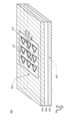
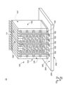
- FIG. 1 is a perspective view showing the configuration of a semiconductor module according to a first embodiment of the present invention.
- FIG. 2 is a perspective view showing a plurality of inductors included in a logic chip and a group of inductors included in a plurality of memory chips according to a first embodiment of the present invention.
- 3(A) is a perspective view showing the configuration of the inductor on the logic chip and the inductor on the memory chip shown in FIG. 2
- FIG. 3(B) is a perspective view showing the structure of the inductor on the logic chip and the inductor on the memory chip shown in FIG.
- FIG. 1 is a block diagram showing the configuration of a semiconductor module according to a first embodiment of the present invention.
- FIG. 1 is a perspective view showing the configuration of a memory chip according to a first embodiment of the present invention. 6 is a cross-sectional view showing the cross-sectional structure of the memory chip taken along line A1-A2 shown in FIG. 5.
- FIG. FIG. 1 is a block diagram showing the configuration of a memory chip according to a first embodiment of the present invention.
- FIG. 2 is a plan view showing the configuration of an inductor group included in the memory chip according to the first embodiment of the present invention.
- FIG. 1 is a perspective view showing the configuration of a logic chip according to a first embodiment of the present invention.
- 10 is a cross-sectional view showing the cross-sectional structure of the logic chip taken along the line B1-B2 shown in FIG. 9.
- FIG. 1 is a block diagram showing the configuration of a logic chip according to a first embodiment of the present invention.
- FIG. 2 is a plan view showing the configuration of an inductor group included in the logic chip according to the first embodiment of the present invention.
- 1 is a perspective view and a schematic diagram showing the configurations of an inductor included in a logic chip and an inductor included in a memory chip according to a first embodiment of the present invention.
- FIG. FIG. 3 is a schematic diagram showing the positional relationship of inductor groups included in each of a plurality of memory chips according to the first embodiment of the present invention.
- FIG. 2 is a schematic diagram showing the positional relationship of an inductor group included in the logic chip according to the first embodiment of the present invention.
- FIG. 2 is a schematic diagram showing the relationship between an inductor group included in a logic chip and a memory chip (an inductor group included in a memory chip) during inductor communication according to the first embodiment of the present invention.
- 17(A) to 17(C) are schematic diagrams showing a method for manufacturing a semiconductor module according to the first embodiment of the present invention.
- 18(A) to 18(C) are schematic diagrams showing a method for manufacturing a semiconductor module according to the first embodiment of the present invention.
- FIG. 2 is a schematic diagram showing the configuration of a semiconductor module according to a comparative example.
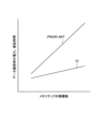
- 7 is a graph showing power and delay time during data communication with respect to the stacked number of memory chips in the semiconductor module according to the first embodiment of the present invention and the semiconductor module according to a comparative example.
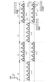
- FIG. 7 is a schematic diagram showing the positional relationship of an inductor group included in a logic chip according to a second embodiment of the present invention.
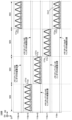
- FIG. 7 is a schematic diagram showing the relationship between an inductor group included in a logic chip and a memory chip (an inductor group included in a memory chip) during inductor communication according to a second embodiment of the present invention.
- FIG. 7 is a schematic diagram showing the positional relationship of inductor groups included in each of a plurality of memory chips according to a second embodiment of the present invention.
- 24(A) and 24(B) are schematic diagrams showing a method for manufacturing a semiconductor module according to a second embodiment of the present invention.
- FIG. 1 is a schematic diagram showing the positional relationship of an inductor group included in a logic chip according to a second embodiment of the present invention.
- FIG. 7 is a schematic diagram showing the positional relationship of inductor groups included in each of a plurality of memory chips according to a third embodiment of the present invention.
- FIG. 7 is a schematic diagram showing the positional relationship of an inductor group included in a logic chip according to a third embodiment of the present invention.
- FIG. 7 is a schematic diagram showing the relationship between an inductor group included in a logic chip and a memory chip (an inductor group included in a memory chip) during inductor communication according to a third embodiment of the present invention.
- 28(A) to 28(D) are schematic diagrams showing a method for manufacturing a semiconductor module according to a third embodiment of the present invention.
- FIG. 29(A) and 29(B) are schematic diagrams showing a method for manufacturing a semiconductor module according to a third embodiment of the present invention.
- 30(A), FIG. 30(B), and FIG. 30(C) are schematic diagrams showing a method for manufacturing a semiconductor module according to a fourth embodiment of the present invention.
- 31(A) and 31(B) are schematic diagrams showing a method for manufacturing a semiconductor module according to a fourth embodiment of the present invention.
- FIG. 32(A) is a plan view showing the configuration of an inductor included in a seal ring and a memory chip according to the fifth embodiment of the present invention
- FIG. 32(B) is a plan view taken along line C1-C2 in FIG.
- FIG. 33(A) is a plan view showing the configuration of an inductor included in a seal ring and a logic chip according to the fifth embodiment of the present invention
- FIG. 33(B) is a plan view taken along the line J1-J2 in FIG. 33(A).
- FIG. 34(A) is a plan view showing the configuration of an inductor included in a seal ring and a memory chip according to the fifth embodiment of the present invention
- FIG. 34(B) is a plan view taken along the line E1-E2 in FIG. FIG.
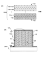
- FIG. 35(A) is a plan view showing a method of manufacturing an inductor included in a memory cube according to the sixth embodiment of the present invention
- FIG. 35(B) is a side view showing a memory cube and an inductor included in the memory cube.
- FIG. 36(A) is a plan view showing a method for manufacturing an inductor included in a memory cube according to the sixth embodiment of the present invention
- FIG. 36(B) is a plan view taken along line F1-F2 in FIG. 35(A).
- FIG. 3 is a cross-sectional view showing a cross section of a memory cube.
- FIG. 37(A) is a plan view showing a method for manufacturing an inductor included in a memory cube according to the sixth embodiment of the present invention
- FIG. 37(B) is a side view showing a memory cube and an inductor included in the memory cube.
- FIG. 38(A) is a plan view showing a method for manufacturing an inductor included in a memory cube according to the sixth embodiment of the present invention
- FIG. 38(B) is a plan view taken along line G1-G2 in FIG. 37(A).
- FIG. 3 is a cross-sectional view showing a cross section of a memory cube.
- FIG. 7 is a perspective view showing the configuration of a power supply line of a semiconductor module according to a seventh embodiment of the present invention.
- FIG. 40 is a cross-sectional view showing a cross section of the semiconductor module taken along line H1-H2 in FIG. 39.
- 41(A) and 41(B) are side views showing a method for manufacturing a power supply line for a semiconductor module according to a seventh embodiment of the present invention.
- FIG. 7 is a perspective view showing an integrated circuit mounted with a semiconductor module according to an eighth embodiment of the present invention.
- FIG. 43 is a cross-sectional view showing a cross section of the integrated circuit of FIG. 42;
- FIGS. 44(A) to 44(C) are cross-sectional views showing a cross section of an integrated circuit mounted with a semiconductor module according to an eighth embodiment of the present invention. It is a flowchart which shows the mounting method of the semiconductor module based on 9th Embodiment of this invention.
- a member or region when referred to as being “above (or below)” another member or region, it is meant to be directly above (or below) the other member or region, unless otherwise specified. This includes not only the case where it is located directly below (directly below) but also the case where it is above (or below) another member or area, that is, another component is included in between above (or below) another member or area. Including cases.
- the D1 direction intersects the D2 direction
- the D3 direction intersects the D1 direction and the D2 direction (D1D2 plane).
- the D1 direction is called a first direction
- the D2 direction is called a second direction
- the D3 direction is called a third direction.
- the expressions “identical” and “identical” when the expressions “identical” and “identical” are used, the “identical” and “identical” may include errors within the design range. Furthermore, in an embodiment of the present invention, when an error is included in the design range, the expressions “substantially identical” and “substantially matched” may be used.
- FIG. 1 is a perspective view showing the configuration of a semiconductor module 10.
- FIG. 2 is a perspective view showing a plurality of inductors 272 included in the logic chip 200 and an inductor group 171 included in the plurality of memory chips 110.
- 3(A) is a perspective view showing the configuration of the inductor 272 on the logic chip 200 shown in FIG. 2 and the inductor 172 on the memory chip 110
- FIG. 5 is a diagram showing the positional relationship with an inductor 172 on the memory chip 110.
- FIG. FIG. 4 is a block diagram showing the configuration of the semiconductor module 10.
- the semiconductor module 10 includes a memory cube 100, a logic chip 200, and an adhesive layer 300.
- Logic chip 200 is sometimes called a semiconductor chip.
- the memory cube 100 includes a structure in which a plurality of memory chips 110 are stacked, and is arranged on the second surface 204 of the logic chip 200.
- Each of the plurality of memory chips 110 includes a similar configuration.
- Each of the plurality of memory chips 110 includes, for example, a transistor layer 130, a wiring layer 150, and an inductor layer 170.
- the logic chip 200 includes, for example, a transistor layer 230, a wiring layer 250, and an inductor layer 270, and has a first surface 202 parallel to a D1 direction (first direction) and a D2 direction (second direction) that intersects the first direction. , including a first surface 202 and an opposite second surface 204.
- the first surface 202 is a surface opposite to the surface on which the wiring layer 250 is arranged with respect to the transistor layer 230
- the second surface 204 is the surface on the opposite side to the surface on which the wiring layer 250 is arranged with respect to the inductor layer 270. It is a surface.
- Adhesive layer 300 is disposed between second side 146 of memory cube 100 and second side 204 of logic chip 200 and connects memory cube 100 and logic chip 200.
- the inductor layer 170 of each of the plurality of memory chips 110 is arranged in a D3 direction (third direction) perpendicular to the first direction and the second direction (i.e., the first surface 202 and the second surface 204).
- the first inductor includes a plurality of inductors 172 (first inductors) arranged in parallel with each other.
- the logic chip 200 includes a plurality of inductors 272 (second inductors) arranged parallel to the positions where the plurality of inductors 172 are arranged and parallel to and close to the second surface 204 .
- the inductor layer 270 includes a plurality of inductors 272.
- the plurality of memory chips 110 include, for example, a memory chip 110n and a memory chip 110n+1 arranged adjacent to the memory chip 110n.
- Memory chip 110n includes an inductor layer 170n.
- the inductor layer 170n includes a plurality of inductors 172, and the plurality of inductors 172 includes an inductor 172b including one linear side 172bb.
- the memory chip 110n+1 includes an inductor layer 170n+1.
- the inductor layer 170n+1 includes a plurality of inductors 172, and the plurality of inductors 172 includes an inductor 172a including one linear side 172ab. Note that, like the inductors 172b and 172a, one straight side 172bb and one straight side 172ab are close to and parallel to the second surface 204.
- the plurality of inductors 172 are arranged in parallel in the second direction.
- Inductor 172 includes terminal A and terminal B. Although details will be described later, the inductor 172 is electrically connected to the transmitting/receiving circuit 114 using terminals A and B.
- the plurality of inductors 272 are arranged in a matrix in the first direction and the second direction.
- the plurality of inductors 272 include an inductor 272a including one linear side 272ab, and an inductor 272b including one linear side 272bb.
- Inductor 272 includes terminal C and terminal D. Although details will be described later, the inductor 272 is electrically connected to the transmitting/receiving circuit 214 using terminals C and D.
- the shape of the inductor 172 and the shape of the inductor 272 are, for example, triangular. Since the memory chip 110 stands perpendicular to the logic chip 200, the inductor 172 faces the inductor 272 at 90 degrees. Among the plurality of inductors 172 and the plurality of inductors 272, one inductor 172 and one inductor 272 facing each other are magnetically coupled to each other, so that the inductors can communicate with each other on a one-to-one basis. Communication between inductors associated with magnetic field coupling is called, for example, inductor communication, signal communication, data communication, or the like.
- the shape of the inductor 172 and the shape of the inductor 272 are not limited to the triangular shape.
- the shape of the inductor 172 and the shape of the inductor 272 may be trapezoidal or pentagonal.
- the shape of the inductor 172 and the shape of the inductor 272 may be any shape that allows inductor communication.
- inductor 172a and inductor 272a face each other at 90 degrees, and can communicate one-to-one by magnetic field coupling. More specifically, effective inductor communication is performed by the base of the triangle of inductor 172a (one straight side 172ab) and the base of the triangle of inductor 272a overlapping with one straight side 172ab (one straight side 272ab).
- One straight side 172ab mainly has the function of performing inductor communication with one straight side 272ab.
- the two sides other than one straight side 172ab mainly have the function of supplying current to one straight side 172ab.
- inductor 272a Similar to inductor 172a, in inductor 272a, the two sides other than one straight side 272ab mainly have the function of supplying current to one straight side 272ab. Inductor 172b and inductor 272b have the same configuration and function as inductor 172a and inductor 272a.
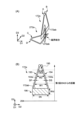
- each of the plurality of inductors 172 includes a first side 193a, extends in the D3 direction, and has a first width DS that is limited in the D2 direction.
- a second portion 194 including a second side 194a and extending in the D3 direction and having a finite second width DS in the D2 direction;
- the third portion 196 includes one linear side (for example, side 172ab), extends in the D2 direction, has a length Dh parallel to the D22 direction, and has a finite third width Wid in the D3 direction.
- the distances (distance W1, distance W2, and distance W3) between the first side 193a and the second side 194a cut parallel to the second surface 204 are the same as the distances (distance W1, distance W2, and distance W3) that are The distance from the second surface 204 becomes shorter. That is, distance W1, distance W2, and distance W3 become shorter in this order.
- the inductor 172a is arranged perpendicularly to the second side surface 146 of the memory cube 100.
- the first side 193a and the second side 194a are defined as lines extending in the D3 direction and D2 direction, and one linear side (for example, 172ab) is defined as a side extending in the D2 direction.
- the shape of the region 195 formed by is triangular. Note that the shape of the region 195 is not limited to a triangular shape.
- the inductor 172a has a fourth part (not shown) including a third side (not shown) between the first side 193a and one straight side, and a fourth part (not shown) that is straight with the second side 194a.
- the region 195 may have a trapezoidal shape including a fifth portion (not shown) including a fourth side (not shown) between one side of the shape, or a pentagonal shape.
- the shape may be a pentagonal shape.
- the shape of the inductor 172a and the shape of the region 195 may be any shape that allows inductor communication.
- Inductor 272a may have a similar configuration and function as inductor 172a. Note that in this specification and the drawings, viewing a plane parallel to the D2 direction and the D3 direction from the D1 direction is referred to as a front view.
- the memory cube 100 includes a plurality of magnetically coupled chip interfaces (Through Chip Interface-IO (TCI-IO)) 112 and a plurality of memory modules 111.
- TCI-IO Through Chip Interface-IO
- the plurality of TCI-IOs 112 are electrically connected to the memory module 111.
- the TCI-IO 112 includes an inductor 172, a transmission/reception circuit 114, and a parallel-to-serial conversion circuit 113.
- Inductor 172 is electrically connected to transmitter/receiver circuit 114 using terminals A and B.
- the transmitter/receiver circuit 114 is electrically connected to the parallel-serial converter circuit 113 .
- Parallel-to-serial conversion circuit 113 is electrically connected to memory module 111 .
- the inductor 172 has a function of contactless inductor communication with the inductor 272 of the logic chip 200.
- the transmitting/receiving circuit 114 has, for example, a function of amplifying the signal (data) received by the inductor 172 and a function of removing noise from the received signal (data). Further, the transmitting/receiving circuit 114 has a function of transmitting, for example, a desired signal (data) converted using the parallel-to-serial converting circuit 113 onto radio waves.
- the signal received by inductor 172 includes multiple parallel signals from logic chip 200.
- the desired signals include multiple parallel signals from memory module 111.
- step 1 the parallel-to-serial conversion circuit 113 performs parallel-to-serial conversion on a large number of parallel signals from the logic chip 200 to convert them into a serial signal (serial signal). Serial signals are transferred at high speed using one signal path (wiring).
- step 2 the parallel-to-serial conversion circuit 113 performs serial-to-parallel conversion on the serial signal immediately before the memory module 111, returns it to a large number of parallel signals, and then transmits the large number of parallel signals to the memory module 111. .
- the parallel-to-serial conversion circuit 113 executes step 1 following step 2, for example.
- the parallel-to-serial conversion circuit 113 is called, for example, a SerDes circuit (Serialize and Deserialize Circuit).
- the memory module 111 includes, for example, a function of generating a large number of parallel signals to be transmitted, and a function of controlling a large number of received parallel signals and storing them in the memory cell array 115 (see FIG. 7).
- the logic chip 200 includes a plurality of magnetic field coupling chip interfaces (Through Chip Interface-IO (TCI-IO)) 212 and a plurality of logic modules 211.
- TCI-IO Through Chip Interface-IO
- the plurality of TCI-IOs 212 are electrically connected to the logic module 211.
- the TCI-IO 212 includes an inductor 272, a transmission/reception circuit 214, and a parallel-to-serial conversion circuit 213.
- Inductor 272 is electrically connected to transmitter/receiver circuit 214 using terminals C and D.
- the transmitter/receiver circuit 214 is electrically connected to the parallel-to-serial converter circuit 213 .
- Parallel-serial conversion circuit 213 is electrically connected to logic module 211 .
- the configurations and functions of the inductor 272, the transmission/reception circuit 214, the parallel-serial conversion circuit 213, and the logic module 211 are the same as those of the inductor 172, the transmission/reception circuit 114, the parallel-serial conversion circuit 113, and the memory module 111. Therefore, descriptions of the configurations and functions of the inductor 272, the transmission/reception circuit 214, the parallel-to-serial conversion circuit 213, and the logic module 211 will be omitted here.
- the semiconductor module 10 includes the functions and configurations described above. Signals are transmitted and received between the inductor 172 included in the memory chip 110 and the inductor 272 included in the logic chip 200 using non-contact inductor communication.
- the distance between the memory chip 110 (inductor 172) and the logic chip 200 (inductor 272) in the semiconductor module 10 is substantially the thickness of the adhesive layer 300.
- the distance between the memory chip 110 (inductor 172) and the logic chip 200 (inductor 272) in the semiconductor module 10 is the distance between the memory chip 110 and the logic chip 200 that are connected using wiring, through electrodes, bumps, etc.
- the memory chip 110 and the logic chip 200 can be bonded to each other using the thin adhesive layer 300 without creating a gap due to the bumps, so that the thermal resistance is low and the heat dissipation characteristics are excellent. Further, since the wiring resistance and parasitic capacitance of the semiconductor module 10 are suppressed, power consumption in communication using the semiconductor module 10 can be suppressed.
- the semiconductor module 10 includes a memory cube 100 in which a plurality of memory chips 110 including a plurality of inductors 172 are stacked, and a large-capacity memory can be realized without increasing the size of the memory chip. That is, the semiconductor module 10 includes a large-capacity memory in which wiring resistance and parasitic capacitance of the semiconductor module 10 are suppressed compared to a module having a large chip size. Therefore, a memory with low power consumption and large capacity can be realized by using the semiconductor module 10.
- the semiconductor module 10 includes a configuration in which one-to-one inductor communication is possible between the inductor 172 and the inductor 272, which are arranged to face each other at 90 degrees. Further, a plurality of inductors 172 are arranged in parallel to the second side surface 146 of the memory cube 100, a plurality of inductors 272 are arranged in parallel to the second surface 204 of the logic chip 200, and the inductors communicate with each other on a one-to-one basis. be able to. As a result, it is easy to communicate large amounts of signals (data) in parallel.
- the semiconductor module 10 includes, for example, a plurality of triangular inductors 172, and the distance between the two sides of the inductor 172 becomes shorter as the distance from the second surface 204 increases. That is, the distance between two adjacent inductors 172 increases as the distance from the second surface 204 increases. Therefore, since two adjacent inductors 172 are unlikely to interfere with each other, the semiconductor module 10 can suppress crosstalk.
- FIG. 5 is a perspective view showing the configuration of the memory chip 110.
- FIG. 6 is a cross-sectional view showing the cross-sectional structure of the memory chip 110 along line A1-A2 shown in FIG.
- FIG. 7 is a block diagram showing the configuration of the memory chip 110.
- FIG. 8 is a plan view showing the configuration of the inductor group 171. Descriptions of configurations that are the same or similar to those in FIGS. 1 to 4 will be omitted here.
- the memory cube 100 includes a configuration in which a plurality of memory chips 110 are stacked in the D1 direction.
- the memory cube 100 includes a first surface 142 parallel to the D2 direction and the D3 direction, and a second surface 144 opposite to the first surface 142 and parallel to the first surface 142 with respect to the D1 direction.
- the memory cube 100 also includes a first side surface 145 perpendicular to the first surface 142 and the second surface 144, a second side surface 146 adjacent to the first side surface 145, a third side surface 147 adjacent to the second side surface 146, and It includes a third side 147 and a fourth side 148 adjacent to the first side 145 .
- the second side surface 146 is in contact with the adhesive layer 300, and the memory cube 100 is placed on the second surface 204 of the logic chip 200.
- each of the plurality of memory chips 110 includes, for example, a transistor layer 130, a wiring layer 150, and an inductor layer 170.
- Each of the plurality of memory chips 110 includes, for example, a memory chip 110n, a memory chip 110n+1 adjacent to the memory chip 110n, a memory chip 110n+2 adjacent to the memory chip 110n+1, a memory chip 110n+3 adjacent to the memory chip 110n+2, and a memory chip 110n+3 adjacent to the memory chip 110n+3.
- the memory chip 110n+4 includes a memory chip 110n+4.
- the memory chip is expressed as a memory chip 110.
- the memory chips are expressed as a memory chip 110n, a memory chip 110n+1, a memory chip 110n+2, etc.
- the inductor group is expressed as an inductor group 171
- the inductor is expressed as an inductor 172.
- the inductor groups 171a, 171b, etc. are expressed as inductor groups 171a, 171b, etc.
- the inductors are expressed as inductors 172a, 172b, etc.
- the memory chip 110 includes a first surface 102 parallel to the D2 direction and the D3 direction, and a second surface 104 opposite to the first surface 102 with respect to the D1 direction.
- the first surface 102 is a surface opposite to the transistor layer 130 on which the wiring layer 150 is disposed
- the second surface 104 is the surface opposite to the surface on which the wiring layer 250 is disposed relative to the inductor layer 170. It is a surface.
- the first surface 102 and the second surface 104 are parallel to the first surface 142 and the second surface 144.
- the memory chip 110 also has a first side surface 105 perpendicular to the first surface 102 and the second surface 104, a second side surface 106 adjacent to the first side surface 105, a third side surface 107 adjacent to the second side surface 106, and It includes a third side 107 and a fourth side 108 adjacent to the first side 105 .
- the first side 105 is a part of the first side 145
- the second side 106 is a part of the second side 146
- the third side 107 is a part of the third side 147
- the fourth side 108 is a part of the second side 145. It is a part of the fourth side surface 148.
- the inductor layer 170 includes a plurality of inductor groups 171.
- Each of the plurality of inductor groups 171 includes a plurality of inductors 172.
- inductor group 171 includes five inductors 172.
- the plurality of inductor groups 171 include a plurality of inductors 172 arranged perpendicularly to the D2 direction and the D3 direction (that is, the first surface 102 and the second surface 104) and parallel to the D3 direction.
- Each of the plurality of inductor groups 171 is arranged apart from the fourth side surface 108 and close to the second side surface 146, and is arranged to extend in the D2 direction.
- the number of the plurality of inductors 172 included in the inductor group 171 is not limited to five. The number of inductors 172 can be changed as appropriate depending on the specifications, usage, etc. of the semiconductor module 10.
- the transistor layer 130 includes, for example, a substrate 173, an element isolation region 174, an activation region 175, a transistor 176, an insulating layer 177, and a portion of a wiring 178.
- the substrate 173 is, for example, a Si substrate or a Si-wafer.
- the wiring layer 150 includes a multilayer wiring structure in which wiring and insulating layers are alternately stacked.
- the wiring layer 150 includes, for example, a part of the wiring 178, an insulating layer 179, a wiring 180, and an insulating layer 181.
- the number of layers of multilayer wiring in wiring layer 150 is not limited to two layers shown in FIG. 6 .
- the number of multilayer wiring layers in the wiring layer 150 may be three or more layers.
- the number of multilayer wiring layers in the wiring layer 150 can be changed as appropriate depending on the specifications, usage, etc. of the semiconductor module 10.
- the inductor layer 170 includes, for example, an insulating layer 182 and a plurality of inductors 172. Further, the inductor layer 170 includes a plurality of inductor groups 171.
- the memory chip 110 includes a plurality of memory modules 111, a plurality of TCI-IOs 112, a power supply wiring 164, and a ground wiring 165.
- Each of the plurality of memory modules 111 includes a memory cell array 115.
- Each of the plurality of TCI-IOs 112 includes a plurality of inductor groups 171, and the inductor group 171 includes a plurality of inductors 172.
- the memory module 111 stores signals (data) in the memory cell array 115, reads signals (data) from the memory cell array 115, transmits signals (data) to the TCI-IO 112, or reads signals (data) from the TCI-IO 112. It has a function to control the reception of data).
- the memory cell array 115 includes a plurality of memory cells (not shown).
- Each of the plurality of memory cell arrays 115 is, for example, an SRAM (Static Random Access Memory), and each of the plurality of memory cells is an SRAM cell. It is a cell.
- the SRAM, the SRAM cell, and the memory module 111 for SRAM can employ technology used in the technical field of SRAM. Therefore, detailed explanation will be omitted here.
- the plurality of memory cell arrays 115 and the plurality of memory cells may be memory cell arrays and memory cells other than SRAM, such as DRAM (Dynamic Random Access Memory), DRAM cells, and MRAM (Magnetoresistive Random Access Memory). Memory) and MRAM cell etc.
- the plurality of memory modules 111 and the plurality of TCI-IOs 112 are electrically connected to a power supply wiring 164 and a ground wiring 165.
- the power supply wiring 164 and the ground wiring 165 are electrically connected to, for example, an external circuit (not shown), and are supplied with power (VDD), VSS, and the like.
- VDD is, for example, 1V or 3V.
- VSS is, for example, a ground voltage, 0V, or the like.
- the plurality of inductor groups 171 are close to the second side surface 106 of the memory chip 110 and are arranged in parallel in the D2 direction.
- Each of the plurality of inductor groups 171 includes a plurality of inductors 172.
- inductor group 171 includes five inductors 172c, 172d, 172e, 172f, and 172g.
- the plurality of inductors 172 include, for example, an inductor having a data communication (data transmission) function and an inductor having a clock communication (clock transmission) function.
- the inductor group 171 is sometimes called a channel.
- the inductor 172c has a function of data communication with the inductor 272 with a one-to-one correspondence, and is called a first data channel (Data Channel 1).
- Inductors 172d, 172f, and 172g have the same function and configuration as inductor 172c, and are connected to the second data channel (Data Channel 2), the third data channel (Data Channel 3), and the fourth data channel (Data Channel 3), respectively. 4) It is called.
- the inductor 172e has a function of clock communication (clock transmission) with the inductor 272 with one-to-one correspondence, and is called a clock channel.
- Each inductor 172 may perform inductor communication with the corresponding inductor 272 on a one-to-one basis (in synchronization) with the clock received through clock communication. (asynchronously), inductor communication may be performed with one-to-one corresponding inductor 272. Further, for example, the inductor 172e does not have a clock communication function and has the same function and configuration as the inductor 172c, and each inductor 172 performs inductor communication with the corresponding inductor 272 on a one-to-one basis in an asynchronous manner. Good too.
- the inductor communication of the semiconductor module 10 can be selected as appropriate based on the specifications, usage, etc. of the semiconductor module 10 without departing from the scope of the present invention.
- the length MCBZ (see FIG. 1) of the memory cube 100 in the D1 direction is 5.12 mm
- the length MCBY (see FIG. 1) of the memory cube 100 in the D2 direction is 5.00 mm
- the length MCBZ (see FIG. 1) of the memory cube 100 in the D3 direction is 5.12 mm
- the length MCBX (see Figure 1) is 5.00 mm.
- the thickness THI (see FIG. 6) of the memory chip 110 is 80 ⁇ m.
- the length MIX (see FIG. 8) of the inductor group 171 parallel to the D2 direction is 600 ⁇ m
- the length MIY (see FIG. 8) of the inductor group 171 parallel to the D3 direction is 160 ⁇ m.
- the memory chip 110 is manufactured using a 2 nm CMOS process
- the memory cube 100 is configured with the above size in which 64 memory chips 110 are stacked
- the inductor group 171 is configured with the above size including four data channels.
- the data transfer rate is 200 Gbps.
- the data rate of one data channel of the inductor 172 and the inductor 272 is 50 Gbps
- the frequency of the system clock of the clock channel is 0.5 GHz
- the clock frequency of the transmitting/receiving circuits 114 and 214 is 250 GHz.
- FIG. 9 is a perspective view showing the configuration of the logic chip 200.
- FIG. 10 is a cross-sectional view showing the cross-sectional structure of the logic chip 200 taken along the line B1-B2 shown in FIG.
- FIG. 11 is a block diagram showing the configuration of the logic chip 200.
- FIG. 12 is a plan view showing the configuration of the inductor group 271. Descriptions of configurations that are the same or similar to those in FIGS. 1 to 8 will be omitted here.
- the semiconductor module 10 includes a first surface 202 parallel to the D1 direction and the D2 direction, and a second surface 204 opposite to the first surface 202.
- the first surface 202 is a surface opposite to the surface on which the wiring layer 250 is arranged with respect to the transistor layer 230
- the second surface 204 is the surface on the opposite side to the surface on which the wiring layer 250 is arranged with respect to the inductor layer 270. It is a surface.
- the logic chip 200 includes, for example, a transistor layer 230, a wiring layer 250, and an inductor layer 270.
- the inductor layer 170 includes a plurality of inductor groups 271.
- Each of the plurality of inductor groups 271 includes a plurality of inductors 272.
- inductor group 271 includes five inductors 272.
- the plurality of inductor groups 271 are arranged in a matrix in parallel to the D1 direction and the D2 direction (that is, the first surface 202 and the second surface 204).
- the plurality of inductors 172 are arranged in a matrix in parallel to the D1 direction and the D2 direction (that is, the first surface 202 and the second surface 204).
- the number of the plurality of inductors 272 included in the inductor group 271 is not limited to five. The number of inductors 272 can be changed as appropriate depending on the specifications, usage, etc. of the semiconductor module 10.
- the logic chip 200 includes a memory cube placement area 210 approximately in the center.
- the memory cube arrangement area 210 is in contact with the adhesive layer 300, and the adhesive layer 300 is arranged thereon.
- the memory cube 100 is placed on the memory cube placement area 210.
- the memory cube arrangement area 210 overlaps the plurality of inductor groups 271.
- the plurality of inductor groups 271 are arranged inside the memory cube arrangement area 210 when viewed from the front.
- the inductor group is expressed as an inductor group 271 and the inductor is expressed as an inductor 272.
- the inductor groups are expressed as inductor groups 271a, 271b, etc.
- the inductors are expressed as inductors 272a, 272b, etc.
- the transistor layer 230 includes, for example, a substrate 273 including an element isolation region 274 and an activation region 275, a transistor 276a, a transistor 276b, an insulating layer 277, a part of a wiring 278a, and a part of a wiring 278b.
- the substrate 273 is, for example, a Si substrate or a Si-wafer.
- the wiring layer 250 includes a multilayer wiring structure in which wiring and insulating layers are alternately stacked.
- the wiring layer 250 includes, for example, a part of the wiring 278a, a part of the wiring 278b, an insulating layer 279, a wiring 280a, a wiring 280b, and an insulating layer 281.
- the number of layers of multilayer wiring in wiring layer 250 is not limited to two layers shown in FIG. 10.
- the number of layers of multilayer wiring in the wiring layer 250 may be three or more layers.
- the number of multilayer wiring layers in the wiring layer 250 can be changed as appropriate depending on the specifications, usage, etc. of the semiconductor module 10.
- the inductor layer 270 includes, for example, an insulating layer 282 and a plurality of inductors 272 (inductor 272a, inductor 272b). Further, the inductor layer 270 includes a plurality of inductor groups 271.
- the logic chip 200 includes, for example, a plurality of logic modules 211, a plurality of TCI-IOs 212, a plurality of DRAM interfaces (Dynamic Random Access Memory (DRAM) IO) 215, and a plurality of external IOs 216.
- Each of the plurality of TCI-IOs 212 includes a plurality of inductor groups 271, and the inductor group 271 includes a plurality of inductors 272.
- the configuration of the logic chip 200 shown in FIG. 11 is an example, and the configuration of the logic chip 200 is not limited to the example shown in FIG. 11.
- logic chip 200 may not include DRAMIO 215.
- the logic module 211 has a function for controlling the transmission of signals (data) to the TCI-IO 212 or the reception of signals (data) from the TCI-IO 212. Furthermore, the logic module 211 has a function of driving the memory module 111 within the memory chip 110. For example, the logic module 211 transmits a signal for driving the memory module 111 via the TCI-IO 212.
- the logic module 211 may include, for example, an arithmetic circuit such as a CPU (Central Processing Unit).
- the DRAMIO 215 is electrically connected to, for example, the DRAM module 400 (see FIG. 42), and has a function of transmitting and receiving signals between the DRAM module 400 and the logic chip 200.
- the external IO 216 is electrically connected to, for example, the logic chip 200 and an external circuit (not shown, such as a power supply circuit), and has a function of transmitting and receiving signals between the external circuit and the logic chip 200.
- Each of the plurality of logic modules 211 is electrically connected to a part of the plurality of TCI-IOs 212, a part of the plurality of DRAMIOs 215, and a part of the plurality of external IOs.
- Each of the plurality of logic modules 211 is supplied with power (VDD), VSS, etc. from an external circuit, receives a control program stored in the DRAM module 400 from the DRAM module 400, and executes processing of the control program. .
- the plurality of inductor groups 271 are arranged in a matrix in the D1 direction and the D2 direction.
- Each of the plurality of inductor groups 271 includes a plurality of inductors 272.
- inductor group 271 includes five inductors 272c, 272d, 272e, 272f, and 272g.
- the plurality of inductors 272, like the plurality of inductors 172 include, for example, an inductor having a data communication (data transmission) function and an inductor having a clock communication (clock transmission) function.
- the inductor group 271, like the inductor group 171 is sometimes called a channel.
- the inductor 272c has a function of data communication with the inductor 172 with one-to-one correspondence, and the first data channel ( It is called Data Channel 1).
- the inductors 272d, 272f, and 272g have the same function and configuration as the inductor 272c, and are connected to the second data channel (Data Channel 2), the third data channel (Data Channel 3), and the fourth data channel (Data Channel 3), respectively. 4) It is called.
- the inductor 272e has a function of clock communication (clock transmission) with the inductor 172 with one-to-one correspondence, and is called a clock channel.
- each inductor 272 may perform inductor communication with the corresponding inductor 172 on a one-to-one basis in response to (synchronized with) the clock received through clock communication; Inductor communication may be performed with one-to-one corresponding inductor 172 without synchronization (asynchronously).
- the inductor 272e does not have a clock communication function and has the same function and configuration as the inductor 272c, and each inductor 272 performs inductor communication with the corresponding inductor 172 on a one-to-one basis in an asynchronous manner. Good too.
- the length LCX (see FIG. 1) of the logic chip 200 in the D1 direction is 12.00 mm
- the length LCY (see FIG. 1) of the logic chip 200 in the D2 direction is 12.00 mm
- the thickness of the logic chip 200 in the D3 direction is 80 ⁇ m, similar to the thickness THI of the memory chip 110 (see FIG. 1).
- the length LIX (see FIG. 12) of the inductor group 271 parallel to the D2 direction is 600 ⁇ m
- the length LIY (see FIG. 12) of the inductor group 271 parallel to the D1 direction is 160 ⁇ m.
- the logic chip 200 is manufactured using a 2 nm CMOS process, and the inductor group 271 has the above size including four data channels. Further, the data transfer rate, the data rate of one data channel, the frequency of the system clock, and the clock frequencies of the transmitting/receiving circuits 114 and 214 are as described in "1-2. Overview of the memory cube 100."
- FIG. 13 is a perspective view and a schematic diagram showing the configurations of an inductor 272 included in the logic chip 200 and an inductor 172 included in the memory chip 110. Descriptions of configurations that are the same or similar to those in FIGS. 1 to 12 will be omitted here.
- the perspective view of the inductor 172a and the inductor 272a shown in FIG. 13 is an enlarged view with a part of FIG. 2 omitted.
- the plurality of inductors 172 include the inductor 172a including one linear side 172ab, and the plurality of inductors 272 include one linear side 272ab.
- Inductor 272a is included.
- the inductor 172a and the inductor 272a are arranged to face each other at 90 degrees, and one straight side 172ab and one straight side 272ab are close to each other and parallel to each other, and are also parallel to the second surface 204. parallel.
- the plan view of the inductor 172a and the inductor 272a shown in FIG. is shown.
- the memory chip 110 is arranged in the D3 direction (that is, vertically installed) with respect to the second surface 204 of the logic chip 200, the inductor 172a and the inductor 272a are connected to the second surface 204 of the logic chip 200. In contrast, it is arranged in the D3 direction.
- the distance between the inductor 172a and the inductor 272a, and the distance between one straight side 172ab and one straight side 272ab are indicated by a distance Dis.
- the height of the inductor 172a is indicated by height MIDv
- the width of one linear side 172ab in the D3 direction is indicated by width Wid
- the length of the inductor 272a is indicated by the length Dh
- the height of the inductor 272a is indicated by the height LIDv.
- the interval (distance between) the inductors 172 adjacent to each other and the interval (distance between the inductors 272) adjacent to each other are indicated by the interval (distance) Sh.
- the distance Dis is 10 ⁇ m ⁇ 5 ⁇ m (3 ⁇ ), for example, 18 ⁇ m.
- the height MIDv is, for example, 160 ⁇ m
- the width Wid is, for example, 20 ⁇ m
- the length Dh is, for example, 80 ⁇ m
- the height LIDv is, for example, 80 ⁇ m.
- the length Dh may be, for example, four times or more the distance Dis, and may be four times or more the distance Dis and 15 times or less the distance Dis.
- the height MIDv may be, for example, greater than or equal to the length Dh, and may be greater than or equal to the length Dh and less than or equal to 5 times the length Dh.
- the distance Sh may be, for example, 1/4 or more of the length Dh, 1/2 or more of the length Dh, and 2 times or less of the length Dh.
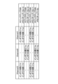
- FIG. 14 is a schematic diagram showing the positional relationship of the inductor groups 171 included in each of the plurality of memory chips 110
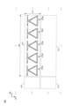
- FIG. 15 is a schematic diagram showing the positional relationship of the plurality of inductor groups 271
- FIG. 16 is a schematic diagram showing the positional relationship of the plurality of inductor groups 271.
- FIG. 2 is a schematic diagram showing the relationship between an inductor group 271 included in a logic chip 200 and a memory chip 110 (an inductor group 171 included in a memory chip 110). Descriptions of configurations that are the same or similar to those in FIGS. 1 to 13 will be omitted here.
- the memory cube 100 includes memory chips 110n to 110n+3, for example, as described in "1-2. Overview of the memory cube 100."
- the memory chip 110n and the memory chip 110n+1 are stacked, for example, so that their inductor layers 170 (see FIG. 1) face each other, and the memory chip 110n+2 and the memory chip 110n+3 are stacked, for example, so that their inductor layers 170 (see FIG. 1) face each other. are stacked so that they are facing each other.
- the memory chip 110n+1 and the memory chip 110n+2 are stacked, for example, so that their transistor layers 130 (see FIG. 1) face each other.
- the inductor groups 171a to 171f shown in FIG. It is shown as follows. Actually, since the memory chips 110n to 110n+3 are arranged (vertical) in the D3 direction with respect to the second surface 204 of the logic chip 200, the inductor groups 171a to 171f are arranged on the second surface 204 of the logic chip 200. It is installed vertically.
- the memory chip 110n includes an inductor group 171b
- the memory chip 110n+1 includes an inductor group 171a and an inductor group 171c
- the memory chip 110n+2 includes an inductor group 171e
- the memory chip 110n+3 includes an inductor group 171d and an inductor group 171f.
- FIG. 14 is an enlarged view of a part of the memory cube 100, and each of the memory chips 110n to 110n+3 includes a plurality of inductor groups 171, and the plurality of inductor groups 171 are arranged apart from each other by a length MIX.
- the inductor group 171a is arranged a length MIX apart from the inductor group 171 adjacent in parallel in the D2 direction (not shown).
- the other inductor groups are arranged a length MIX apart from the inductor group 171 adjacent in parallel in the D2 direction (not shown).
- each of the inductor groups 171a to 171f includes the same configuration and function as the inductor group 171 described with reference to FIG. 8 in "1-2. Overview of the memory cube 100."
- the inductor groups 171a to 171f included in the memory chips 110n to 110n+3 are arranged in a checkered pattern. be done.
- the multiple inductor groups 271 include inductor groups 271a to 271f.
- the inductor groups 271a to 271f are uniformly arranged in a matrix in the D1 and D2 directions.
- Each of the inductor groups 271a to 271f includes the same configuration and function as the inductor group 271 described with reference to FIG. 12 in "1-3. Overview of the logic chip 200".
- One linear side (for example, 272ab) of each of the inductor groups 271a, 271b, and 271c is arranged in parallel, for example, on the boundary between the memory chip 110n and the memory chip 110n+1. Further, one linear side (for example, 272bb) of each of the inductor groups 271d, 271e, and 271f is arranged in parallel, for example, on the boundary between the memory chip 110n+2 and the memory chip 110n+3.
- the thickness THI of the memory chips 110n to 110n+3 and the logic chip 200 is 80 ⁇ m
- the interval between the boundary between the memory chip 110n and the memory chip 110n+1 and the boundary between the memory chip 110n+2 and the memory chip 110n+3 (distance between them) is 160 ⁇ m, which is twice the thickness THI (THI ⁇ 2).
- the length Dh is, for example, 70 ⁇ m
- the interval MIS (distance MIS) between the inductor group 271a and the inductor group 271d in the D1 direction is, for example, 90 ⁇ m. Therefore, in the semiconductor module 10 according to the first embodiment, the thickness THI of the memory chips 110n to 110n+3 and the logic chip 200 is thicker (longer) than the length Dh of one linear side of the inductor 172 and the inductor 272.
- the semiconductor module 10 includes three channels (Channel 1, Channel 2, and Channel 3).
- memory chip 110n and memory chip 110n+2 correspond to an even channel (channel 2)
- memory chip 110n+1 and memory chip 110n+3 correspond to odd channels (channel 1 and channel 3).
- the plurality of inductors 272 of the inductor group 271b included in the logic chip 200 communicate with the plurality of inductors 172 of the inductor group 171b included in the memory chip 110n in one-to-one correspondence through channel 2.
- the plurality of inductors 272 of the inductor group 271a each communicate with the plurality of inductors 172 of the inductor group 171a in one-to-one correspondence through channel 1, and the plurality of inductors 272 of the inductor group 271c each correspond one-to-one.
- the plurality of inductors 272 of the inductor group 271e communicate with the plurality of inductors 172 of the inductor group 171e corresponding one-to-one through channel 2, and the inductor group 271d communicates with the plurality of inductors 172 of the inductor group 171c.
- the plurality of inductors 272 communicate with the plurality of inductors 172 of the inductor group 171d that correspond to each other on a one-to-one basis
- the plurality of inductors 272 of the inductor group 271f communicate with the plurality of inductors 172 of the inductor group 171f that correspond to each other on a one-to-one basis. communicates with the inductor 172 on channel 3.
- the semiconductor module 10 can suppress crosstalk in communication between the logic chip 200 and the memory chip 110n and memory chip 110n+1, which are arranged at substantially the same position. Similarly, crosstalk in communication between the logic chip 200 and the memory chip 110n+2 and the memory chip 110n+3, which are arranged at substantially the same position, can be suppressed.
- the distance MIS between the inductor group 271a and the inductor group 271d in the D1 direction should be approximately the same length as the length Dh of one linear side of the inductor 172 and the inductor 272. is preferred. Thereby, crosstalk in communication between mutually adjacent inductors can be suppressed.
- the inductor Cm1 included in the inductor group 171a of the memory chip 110n+1 is magnetically coupled with the inductor Cl1 included in the inductor group 271a of the logic chip 200, so that inductor communication is possible.
- There is no magnetic field coupling with the inductor Cl4 included in the inductor and there is no crosstalk.
- the inductor Cl1 and the inductor Cl4 are not magnetically coupled and do not have crosstalk.
- FIGS. 17 and 18 are schematic diagrams showing a method of manufacturing the semiconductor module 10. Descriptions of configurations that are the same or similar to those in FIGS. 1 to 16 will be omitted here.
- the stacking (bonding) of memory chips 110 such that their second surfaces 104 on the inductor layer 170 side face each other is called, for example, F2F bonding (Face to Face Fusion).
- the stacking (bonding) of the memory chips 110 such that their first surfaces 102 on the transistor layer 130 side face each other is called, for example, B2B bonding (Back to Back Fusion).
- the stacking (bonding) of the memory chips 110 such that the second surface 104 on the inductor layer 170 side and the first surface 102 on the transistor layer 130 side face each other is called, for example, F2B bonding (Face to Back Fusion).
- the stacking (bonding) of memory chips can be performed using, for example, a technique such as welding (Fusion Bonding) or Silicon Direct Bonding (SDB). Since this is a technique used in the field, a detailed explanation will be omitted here.
- step 1 the second surface 104 of the memory chip 110n and the second surface 104 of the memory chip 110n+1 are stacked (bonded) so as to face each other (see FIG. 17(A)). That is, in step 1, the two memory chips 110n and 110n+1 are joined by F2F junction.
- the thickness THI of the memory chip 110 is, for example, 80 ⁇ m.
- step 2 the memory chip 110n and the memory chip 110n+1 that were F2F bonded in step 1 are bonded to the memory chip 110n+2 and the memory chip 110n+3 that were F2F bonded in the same way as the memory chip 110n and the memory chip 110n+1 (FIG. 17(B) ).
- the first surface 102 on the memory chip 110n+1 side of the bonded memory chip 110n and memory chip 110n+1 is bonded to the first surface 102 on the memory chip 110n+2 side of the bonded memory chip 110n+2 and memory chip 110n+3. That is, the four memory chips 110n to 110n+3 are B2B bonded.
- the memory chips 110n to 110n+3 that were B2B bonded in step 2 are B2B bonded to the memory chips 110n+4 to 110n+7 that were B2B bonded similarly to the memory chips 110n to 110n+3 (see FIG. 17(C)).
- the first surface 102 on the memory chip 110n+1 side of the bonded memory chip 110n and memory chip 110n+1 is bonded to the first surface 102 on the memory chip 110n+2 side of the bonded memory chip 110n+2 and memory chip 110n+3. That is, the four memory chips 110n to 110n+3 are B2B bonded.
- the thickness of the two memory chips 110 combined is, for example, 160 ⁇ m, which is twice the thickness THI.
- memory chips 110n to 110n+63 are stacked (bonded) to form a memory cube 100 in which 64 layers of memory chips 110 are stacked (FIG. 18( (See A).
- the first side 145, second side 146, third side 147, and fourth side of the memory cube 100 are, for example, polished and planarized.
- CMP chemical mechanical polishing
- the memory cube 100 is placed on the logic chip 200 using the adhesive layer 300.
- the second side 146 of the memory cube 100 is connected to the adhesive layer 300, and the second side 146 of the memory cube 100 and the adhesive layer 300 are bonded onto the second side 204 of the logic chip 200 (FIG. 18).
- the adhesive layer 300 may be, for example, an adhesive containing an epoxy resin or an acrylic polymer, or may be a die bonding film containing an epoxy resin or an acrylic polymer, or a die attached film. It may also be an adhesive film such as.
- step 8 the second surface 204 of the logic chip 200 on which the adhesive layer 300 is not disposed, the first surface 142 and the second surface 144 of the memory cube 100, and the fourth side surface 148 of the memory cube 100 are A heat dissipation layer 152 is stacked so as to be in contact with each other (see FIG. 18(C)).
- the fourth side surface 148 is a surface opposite to the second side surface 146 with respect to the D2 direction.
- the heat dissipation layer 152 may be called a heat dissipation plate.
- the thickness THI of the plurality of memory chips 110 can be processed with an accuracy of thickness THI ⁇ 1.3 ⁇ m (3 ⁇ ).
- the position of the inductor 172 is, for example, a design value of ⁇ 4 ⁇ m (3 ⁇ ) in a memory cube 100 in which 64 layers of memory chips 110 are stacked.
- the positioning accuracy of the chip bonder that mounts the memory cube 100 on the logic chip 200 is a design value of ⁇ 2 ⁇ m (3 ⁇ ). Therefore, for example, the horizontal position of the inductor 172 (for example, one linear side 172ab) when mounted is the design value ⁇ 4.5 ⁇ m (3 ⁇ ).
- the distance Dis between the inductor 172 and the inductor 272 is 10 ⁇ m as a design value
- the variation in the horizontal position of the inductor 172 for example, one linear side 172ab
- the length Dh of one straight side 172ab and 272ab of the inductor is designed so that the inductor can communicate even if the distance Dis is 11 ⁇ m.
- FIG. 19 is a schematic diagram showing the configuration of a semiconductor module according to a comparative example
- FIG. 20 is a diagram showing the power and power during data communication with respect to the stacked number of memory chips between the semiconductor module 10 and the semiconductor module 500 according to the comparative example (PRIOR ART). It is a graph showing delay time. Descriptions of configurations that are the same or similar to those in FIGS. 1 to 18 will be omitted here.
- the semiconductor module 500 includes a configuration in which a plurality of memory chips 510 and logic chips 520 are stacked in the D3 direction.
- Each of the plurality of memory chips 510 includes a protection circuit 512, an interface 514 electrically connected to the protection circuit 512, and a memory module 516 electrically connected to the interface 514.
- Logic chip 520 includes a protection circuit 512 , an interface 524 electrically connected to protection circuit 512 , and a logic module 526 electrically connected to interface 524 .
- the protection circuits 512 included in the plurality of memory chips 510 and the protection circuits 512 included in the logic chip 520 are connected using through electrodes 530 formed in parallel to the D3 direction.
- a plurality of memory chips 510 are connected by through electrodes 530 made of copper (Cu), for example.
- the length of the through electrode 530 increases in proportion to the number of stacked memory chips 510, so that parasitic capacitance such as wiring resistance and wiring capacitance associated with the through electrode 530 increases. growing.
- the power during data communication and the delay time required for communication increase in proportion to the number of stacked memory chips 510.
- the amount of noise such as power supply noise (switching noise) also increases.
- the distance between the plurality of inductors 172 included in the memory cube 100 and the inductors 272 included in the logic chip 200 that correspond one-to-one is determined by the distance between the inductors 172 and the inductors 272 that correspond one-to-one.
- Inductor 172 and inductor 272, which are substantially the same and correspond to each other on a one-to-one basis, are capable of non-contact inductor communication. Therefore, parasitic capacitance such as wiring resistance and wiring capacitance of the semiconductor module 10 can be made smaller than that of the semiconductor module 500. Therefore, as shown in FIG. 20, the semiconductor module 10 is capable of lower power consumption and higher speed communication than the semiconductor module 500. Further, the semiconductor module 10 can also reduce the amount of noise such as power supply noise (switching noise) more than the semiconductor module 500.
- FIG. 21 is a schematic diagram showing the positional relationship of the inductor group 171 included in each of the plurality of memory chips 110 according to the second embodiment
- FIG. FIG. 23 is a schematic diagram showing the positional relationship of the inductor group 271, and FIG. 171)
- FIGS. 24(A) and 24(B) are schematic diagrams showing a method for manufacturing a semiconductor module 10A according to the second embodiment of the present invention. Descriptions of configurations that are the same or similar to those in FIGS. 1 to 20 will be omitted here.
- the semiconductor module 10A includes a memory cube 100A and a logic chip 200A.
- the memory cube 100 includes 64 layers of memory chips 110
- the memory cube 100A includes 128 layers of memory chips 110.
- the arrangement of the inductor group 171 of the memory cube 100A and the inductor group 271 of the logic chip 200A is different from the arrangement of the inductor group 171 of the memory cube 100 and the inductor group 271 of the logic chip 200.
- Other functions and configurations of the memory cube 100A and the logic chip 200A are the same as those of the memory cube 100 and the logic chip 200, so detailed explanations are omitted here.
- the memory cube 100 includes, for example, a configuration similar to the configuration described in “1-2. Overview of the memory cube 100”.
- memory cube 100 includes memory chips 110n to 110n+5.
- the memory chip 110n and the memory chip 110n+1, the memory chip 110n+2 and the memory chip 110n+3, and the memory chip 110n+4 and the memory chip 110n+5 are stacked, for example, so that their inductor layers 170 (see FIG. 1) face each other.
- the memory chip 110n+1 and the memory chip 110n+2, and the memory chip 110n+3 and the memory chip 110n+4 are stacked such that their transistor layers 130 (see FIG. 1) face each other.
- the inductor groups 171a to 171f shown in FIG. They are shown parallel to each other.
- Memory chip 110n includes an inductor group 171a
- memory chip 110n+1 includes an inductor group 171c
- memory chip 110n+2 includes an inductor group 171b
- memory chip 110n+3 includes an inductor group 171d
- memory chip 110n+4 includes an inductor group 171e
- Memory chip 110n+5 includes an inductor group 171f.
- FIG. 21 is an enlarged view of a part of the memory cube 100A.
- Each of the memory chips 110n to 110n+5 includes a plurality of inductor groups 171, and the plurality of inductor groups 171 in the same memory chip 110 are arranged at a distance of three times the length LIX from each other in the D2 direction.
- the inductor group 171a is arranged at a distance of three times the length MIX from the inductor group 171 adjacent in parallel in the D2 direction (not shown).
- the other inductor groups are arranged at a distance of three times the length MIX from the inductor group 171 adjacent in parallel in the D2 direction (not shown).
- the inductor groups 171 are spaced apart by a length MIX.
- the inductor group 171a included in the memory chip 110n is arranged a length MIX apart from the inductor group 171b included in the memory chip 110n+1. Similar to the memory chip 110n and the memory chip 110n+1, the same applies to the inductor groups included in the memory chips 110n+2 to 110n+5.
- each of the inductor groups 171a to 171f includes the same configuration and function as the inductor group 171 described with reference to FIG. 8 in "1-2. Overview of the memory cube 100.”
- the plurality of inductor groups 271 include inductor groups 271a to 271f.
- the inductor groups 271a to 271f are arranged in a checkered pattern in the D1 direction and the D2 direction.
- Each of the inductor groups 271a to 271f includes the same configuration and function as the inductor group 271 described with reference to FIG. 12 in "1-3. Overview of the logic chip 200.”
- One linear side (for example, 272ab) of each of the inductor groups 271a and 271c is arranged in parallel, for example, on the boundary between the memory chip 110n and the memory chip 110n+1.
- One linear side (for example, 272ab) of each of the inductor groups 271b and 271d is arranged in parallel, for example, on the boundary between the memory chip 110n+2 and the memory chip 110n+3.
- one linear side (for example, 272bb) of each of the inductor groups 271e and 271f is arranged in parallel on the boundary between the memory chips 110n+4 and 110n+5, for example.
- the interval between the boundary between the memory chip 110n and the memory chip 110n+1 and the boundary between the memory chip 110n+2 and the memory chip 110n+3 (distance between them) is 80 ⁇ m, which is twice the thickness THI (THI ⁇ 2).
- the interval (distance) between the boundary between the memory chip 110n+2 and the memory chip 110n+3 and the boundary between the memory chip 110n+4 and the memory chip 110n+5 is 80 ⁇ m, which is twice the thickness THI (THI ⁇ 2).
- the length Dh is, for example, 70 ⁇ m
- the interval MIS (distance MIS) between the inductor group 271a and the inductor group 271e in the D1 direction is, for example, 80 ⁇ m. Therefore, in the semiconductor module 10 according to the second embodiment, the thickness THI (40 ⁇ m) of the memory chips 110n to 110n+5 and the logic chip 200 is smaller than the length Dh (70 ⁇ m) of one linear side of the inductor 172 and the inductor 272. Thin (short).
- the semiconductor module 10A includes four channels (Channel 1, Channel 2, Channel 3, and Channel 4).
- memory chip 110n and memory chip 110n+4 correspond to channel 1
- memory chip 110n+2 corresponds to channel 2
- memory chip 110n+1 and memory chip 110n+5 correspond to channel 3
- memory chip 110n+3 corresponds to channel 4.
- the plurality of inductors 272 of the inductor group 271a included in the logic chip 200A communicate with the plurality of inductors 172 of the inductor group 171a included in the memory chip 110n on a one-to-one basis through channel 1.
- the plurality of inductors 272 of the inductor group 271b included in the logic chip 200A communicate with the plurality of inductors 172 of the inductor group 171b included in the memory chip 110n+2 on a one-to-one basis through channel 2, and the inductors included in the logic chip 200A
- the plurality of inductors 272 of the group 271c each communicate one-to-one with the plurality of inductors 172 of the inductor group 171c included in the corresponding memory chip 110n+1 through channel 3, and communicate with the plurality of inductors 272 of the inductor group 271d included in the logic chip 200A.
- the plurality of inductors 172 of the inductor group 171e included in the corresponding memory chip 110n communicate through channel 1, and the plurality of inductors 272 of the inductor group 271f included in the logic chip 200A are included in the corresponding memory chip 110n+5 on a one-to-one basis.
- the channel 3 communicates with the plurality of inductors 172 of the inductor group 171f.
- the semiconductor module 10A can suppress crosstalk in communication between the memory chip 110 and the logic chip 200.
- the thickness THI of the plurality of memory chips 110 can be processed with an accuracy of thickness THI ⁇ 1.3 ⁇ m (3 ⁇ ).
- the position of the inductor 172 is, for example, ⁇ 6 ⁇ m (3 ⁇ ) of the design value in the memory cube 100 in which 128 layers of memory chips 110 are stacked.
- the distance MIS between the inductor group 271a and the inductor group 271e in the D1 direction be approximately the same length as the length Dh of one linear side of the inductor 172 and the inductor 272. Thereby, crosstalk in communication between mutually adjacent inductors can be suppressed.
- the inductor Cm1 included in the inductor group 171a of the memory chip 110n is magnetically coupled with the inductor Cl1 included in the inductor group 271a of the logic chip 200A, so that inductor communication is possible. There is no magnetic field coupling with the inductor Cl4 included in the inductor, and there is no crosstalk. Further, the inductor Cl1 and the inductor Cl4 are not magnetically coupled and do not have crosstalk.
- FIG. 24(A) and 24(B) are schematic diagrams showing a method for manufacturing the semiconductor module 10A. Descriptions of configurations that are the same or similar to those in FIGS. 1 to 23 will be omitted here.
- the manufacturing method of the semiconductor module 10A is the same as the manufacturing method described in "1-6.
- steps 1 to 6 are executed to stack 64 layers of memory chips 110.
- step 9 two blocks in which 64 layers of memory chips 110 are stacked are bonded B2B to form a memory cube 100A in which 128 layers of memory chips 110 are stacked (see FIG. 24(A)). ).
- step 10 the memory is Cube 100A is placed on logic chip 200A using adhesive layer 300, and heat dissipation layer 152 is laminated (see FIG. 24(B)).
- FIG. 25 is a schematic diagram showing the positional relationship of the inductor group 171 included in each of the plurality of memory chips 110 according to the third embodiment of the invention
- FIG. 26 is a logic chip 200B according to the third embodiment of the invention
- FIG. 27 is a schematic diagram showing the positional relationship between the inductor group 271 included in the inductor group 271 included in the inductor group 271 and the memory chip 110 (included in the memory chip) included in the logic chip 200C during inductor communication according to the third embodiment of the present invention.
- 29(B) are schematic diagrams showing the relationship between the semiconductor module and the inductor group 171) according to the third embodiment of the present invention.
- 10B is a schematic diagram showing a manufacturing method of 10B. Descriptions of configurations that are the same or similar to those in FIGS. 1 to 24 will be omitted here.
- the semiconductor module 10B includes a memory cube 100B and a logic chip 200B.
- the memory cube 100B includes 128 layers of memory chips 110.
- the arrangement of the inductor group 171 of the memory cube 100B and the inductor group 271 of the logic chip 200B is different from the arrangement of the inductor group 171 of the memory cube 100 and the inductor group 271 of the logic chip 200.
- Other functions and configurations of the memory cube 100B and the logic chip 200B are the same as those of the memory cube 100 and the logic chip 200, so detailed explanations are omitted here.
- the memory cube 100B includes, for example, the same configuration as that described in "1-2. Overview of the memory cube 100.”
- memory cube 100 includes memory chips 110n to 110n+4.
- the memory chip 110n and the memory chip 110n+1, the memory chip 110n+1 and the memory chip 110n+2, the memory chip 110n+2 and the memory chip 110n+3, and the memory chip 110n+3 and the memory chip 110n+4 are stacked such that, for example, the inductor layer 170 and the transistor layer 130 face each other. Ru.
- the memory chip 110n includes an inductor group 171a
- the memory chip 110n+1 includes an inductor group 171b
- the memory chip 110n+2 includes an inductor group 171c
- the memory chip 110n+3 includes an inductor group 171d
- the memory chip 110n+4 includes an inductor group 171e.
- FIG. 25 is an enlarged view of a part of the memory cube 100B.
- each of the memory chips 110n to 110n+4 includes a plurality of inductor groups 171, and the plurality of inductor groups 171 in the same memory chip 110 are arranged at a distance of three times the length LIX from each other in the D2 direction. Ru. Note that each of the inductor groups 171a to 171e includes the same configuration and function as the inductor group 171 described with reference to FIG. 8 in "1-2. Overview of the memory cube 100.”
- the plurality of inductor groups 271 include inductor groups 271a to 271e.
- the inductor group 271b is arranged apart from the inductor group 271a by a length LIX in the D2 direction and a thickness THI (40 ⁇ m) in the D1 direction.
- the inductor group 271c is arranged apart from the inductor group 271b by a length LIX in the D2 direction and a thickness THI (40 ⁇ m) in the D1 direction.
- the inductor group 271d is arranged apart from the inductor group 271b by a length LIX in the D2 direction and a thickness THI (40 ⁇ m) in the D1 direction.
- the inductor group 271e is arranged at a distance of four times the thickness THI (40 ⁇ m) from the inductor group 271a in the D1 direction. Note that each of the inductor groups 271a to 271e includes the same configuration and function as the inductor group 271 described with reference to FIG. 12 in "1-3. Overview of the logic chip 200.”
- One linear side (for example, 272ab) of the inductor group 271a is arranged parallel to the position where the inductor 272a of the memory chip 110n is arranged. Similar to the inductor group 271a, one linear side (for example, 272ab) of the inductor group 271b is arranged parallel to the position where the inductor 272b of the memory chip 110n+1 is arranged, and one linear side of the inductor group 271c Two sides (for example, 272ab) are arranged parallel to the position where the inductor 272c of the memory chip 110n+2 is arranged, and one straight side (for example, 272ab) of the inductor group 271d is arranged above the position where the inductor 272c of the memory chip 110n+3 is arranged.
- One linear side (for example, 272ab) of the inductor group 271e is arranged parallel to the position where the inductor 272e of the memory chip 110n+4 is arranged.
- the thickness THI is, for example, 40 ⁇ m
- the length Dh is, for example, 70 ⁇ m
- the interval MIS (distance MIS) between the inductor group 271a and the inductor group 271e in the D1 direction is, for example, 80 ⁇ m. Therefore, in the semiconductor module 10B according to the third embodiment, the thickness THI (40 ⁇ m) of the memory chips 110n to 110n+4 and the logic chip 200 is smaller than the length Dh (70 ⁇ m) of one linear side of the inductor 172 and the inductor 272. Thin (short).
- the semiconductor module 10B has four channels (Channel 1, Channel 2, Channel 3, Channel 4) like the semiconductor module 10A. including. Memory chip 110n and memory chip 110n+4 correspond to channel 1, memory chip 110n+2 corresponds to channel 2, memory chip 110n+1 corresponds to channel 3, and memory chip 110n+3 corresponds to channel 4.
- the plurality of inductors 272 of the inductor group 271a included in the logic chip 200C communicate with the plurality of inductors 172 of the inductor group 171a included in the memory chip 110n in one-to-one correspondence through channel 1, respectively.
- the plurality of inductors 272 of the inductor group 271b included in the logic chip 200C communicate with the plurality of inductors 172 of the inductor group 171b included in the memory chip 110n+1 on a one-to-one basis through channel 2, and the inductors included in the logic chip 200C
- the plurality of inductors 272 of the group 271c each communicate one-to-one with the plurality of inductors 172 of the inductor group 171c included in the corresponding memory chip 110n+2 through channel 3, and communicate with the plurality of inductors 272 of the inductor group 271d included in the logic chip 200C.
- the semiconductor module 10B can suppress crosstalk in communication between the memory chip 110 and the logic chip 200B.
- FIGS. 28(A) to 28(D), FIG. 29(A), and FIG. 29(B) are schematic diagrams showing a method for manufacturing the semiconductor module 10B. Descriptions of configurations that are the same or similar to those in FIGS. 1 to 27 will be omitted here.
- step 21 F2B bonding is performed so that the second surface 104 of the memory chip 110n and the first surface 102 of the memory chip 110n+1 face each other (see FIG. 28(A)).
- the thickness THI of the memory chip 110 is, for example, 40 ⁇ m.
- step 22 F2B bonding is performed such that the second surfaces 104 on the memory chip 110n+1 side of the memory chip 110n and memory chip 110n+1, which were F2B bonded in step 1, face the first surface 102 of the memory chip 110n+2 ( (See FIG. 28(B)).
- step 23 the second surface 104 of the memory chip 110n+2, which was F2B bonded in step 2, is F2B bonded to the first surface 102 of the memory chip 110n+3 (see FIG. 28(C)).
- step 23 124 By repeating the same steps as step 23 124 times, the memory chips 110n to 110n+127 are stacked (joined) by F2B coupling of the chips, and a memory cube 100B in which 128 layers of memory chips 110 are stacked is formed. (See FIG. 28(D)). Similar to the memory cube 100, the first side 145, second side 146, third side 147 (not shown), and fourth side of the memory cube 100B are flattened by, for example, polishing.
- the memory cube 100B is placed on the logic chip 200B using the adhesive layer 300, and the second surface 204 of the logic chip 200B on which the adhesive layer 300 is not placed and the memory cube 100B are placed on the logic chip 200B using the adhesive layer 300.
- a heat dissipation layer 152 is laminated so as to be in contact with the first surface 142 and second surface 144 of the memory cube 100B and the fourth side surface 148 of the memory cube 100B (see FIG. 29(B)).
- FIGS. 30(A) to 31(B) are schematic diagrams showing a method for manufacturing a semiconductor module according to the fourth embodiment of the present invention. It is. Descriptions of configurations that are the same or similar to those in FIGS. 1 to 29(B) will be omitted here.
- the memory cube 100 includes, for example, memory chips 110n to 110n+3, and includes a configuration similar to the configuration described in "1-6. Example of manufacturing method of semiconductor module 10.” That is, the memory chip 110n and the memory chip 110n+1 are connected F2F, the memory chip 110n+2 and the memory chip 110n+3 are connected F2F, and the memory chip 110n+1 and the memory chip 110n+2 are connected B2B.
- the positions of the memory chips 110n to 110n+3 in the D3 direction corresponding to the second side surface 146 of the memory cube 100 vary.
- the height MIDv of the inductor 172 is 160 ⁇ m
- the width Wid of one linear side 172ab of the inductor 172 is 20 ⁇ m.
- the ends of the memory chips 110n to 110n+3 corresponding to the second side surface 146 are made flat so that the second side surface 146 of the memory cube 100 is flat. (polished portion 190) is polished.
- the memory cube 100 is arranged so that the second side surface 146 is in contact with the adhesive layer 300 with one linear side 172ab exposed to the second side surface 146, and the memory cube 100 and an adhesive layer 300 are disposed on the second side 104 of the logic chip 200 .
- the alignment accuracy MAL between the memory cube 100 and the logic chip 200 is, for example, ⁇ 5 ⁇ m with respect to the boundary between the memory chip 110n and the memory chip 110n+1 (the boundary between the memory chip 110n+2 and the memory chip 110n+3).
- the distance DSF between one of the plurality of linear sides 172ab and the second surface 204 is approximately the same.
- the distance DFS is the same as the thickness of the adhesive layer 300 and the distance Dis.
- the distance DFS is 15 ⁇ m or more and 20 ⁇ m or less.
- the memory cube 100 may be formed by, for example, a plurality of memory chips 110n to 110n+3 having different thicknesses THI.
- the thickness THI4 of the memory chip 110n+3 is thicker than the thickness THI of the memory chip 110n
- the thickness THI of the memory chip 110n is thicker than the thickness THI3 of the memory chip 110n+3
- the thickness THI3 of the memory chip 110n+3 is Thickness is thicker than THI2.
- FIG. 32(A) is a plan view showing the configuration of the seal ring 160 and the inductor 172 included in the memory chip 110 according to the fifth embodiment of the present invention
- FIG. 3 is a cross-sectional view showing a cross section of the seal ring 160 and the inductor 172 included in the memory chip 110 along line C2.
- FIG. 33(A) is a plan view showing the configuration of a seal ring 260 and an inductor 272 included in the logic chip 200 according to the fifth embodiment of the present invention
- FIG. 34(A) is a plan view showing the configuration of the seal ring 160 and the inductor 172 included in the memory chip 110 according to the fifth embodiment of the present invention
- FIG. 34(B) is a plan view showing the configuration of E1-
- FIG. 3 is a cross-sectional view showing a cross section of the seal ring 160 and the inductor 172 included in the memory chip 110 along line E2. Descriptions of configurations that are the same or similar to those in FIGS. 1 to 31(B) will be omitted here.
- the memory cube 100 includes a seal ring 160.
- the seal ring 160 is provided on the outer peripheral portion 192 and formed on the wiring layer 150.
- the inductor 172 is formed to ride over (straddle) the seal ring 160. At least a portion of inductor 172 is disposed outside outer circumferential portion 192 .
- the wiring layer 150 includes a multilayer wiring structure.
- the wiring layer 150 includes, for example, a multilayer wiring structure of six layers (first to sixth layers).
- the six-layer multilayer wiring structure includes an insulating layer 151a, a wiring 151b, an insulating layer 152a, a wiring 152b, an insulating layer 153a, a wiring 153b, an insulating layer 154a, a wiring 154b, an insulating layer 155a, a wiring 155b, an insulating layer 156a, and a wiring 156b. including.
- a first insulating layer 151a is formed on the transistor layer 130, and a first wiring 151b is formed on the transistor layer 130 by penetrating the insulating layer 151a.
- a second insulating layer 152a is formed on the insulating layer 151a and the wiring 151b, and a second wiring 152b is formed on the wiring 151b by penetrating the insulating layer 152a.
- An insulating layer 156a and a wiring 156b are formed.
- the inductor layer 170 is formed on the wiring layer 150.
- the inductor layer 170 includes, for example, an insulating layer 182 and a wiring 183 forming the inductor 172.
- the seal ring 160 has a function of suppressing the absorption of moisture and the intrusion of impurities from the second side surface 146 of the memory cube 100. As a result, by using the seal ring 160, the semiconductor module 10 can suppress corrosion, deterioration, etc. of the inductor 172 due to moisture absorption and intrusion of impurities.
- the logic chip 200 includes a seal ring 260.
- the seal ring 260 is provided on the outer peripheral portion 298 and formed on the wiring layer 250.
- Inductor 272 is placed inside seal ring 260.
- the wiring layer 250 includes a multilayer wiring structure.
- the wiring layer 250 includes, for example, a multilayer wiring structure of six layers (first to sixth layers).
- the six-layer multilayer wiring structure includes an insulating layer 251a, a wiring 251b, an insulating layer 252a, a wiring 252b, an insulating layer 253a, a wiring 253b, an insulating layer 254a, a wiring 254b, an insulating layer 255a, a wiring 255b, an insulating layer 256a, and a wiring 256b.
- the multilayer wiring structure of the wiring layer 250 includes the same configuration and function as the multilayer wiring structure of the wiring layer 150, so a detailed description of the wiring layer 250 will be omitted here.
- the inductor 172 may be formed using multiple wiring lines.
- the inductor 172 is formed using five layers of wiring shown in FIGS. 34(A) and 34(B).
- the wirings 154b, 155b, and 156b are formed with the same wiring as the multilayer wiring in the fourth to sixth layers of the wiring layer 150, and the wiring 184 is formed in the inductor layer 170. be done.
- the wirings 154b, 155b, 156b, 184, and 183 are formed in this order from the lower layer to the upper layer, and are electrically connected to each other.
- Insulating layers 182, 156a, 155a, and 154a are formed in the region where inductor 172 straddles seal ring 160.
- the insulating layers 182, 156a, 155a, and 154a are formed using, for example, an insulating material different from a material with a low dielectric constant (low-k material).
- the insulating material forming the insulating layers 182, 156a, 155a, and 154a is, for example, SiO 2 , SiCN, SiN, SiON, or the like.
- a method for forming an inductor 172 will be described with reference to FIGS. 35(A) to 38(B).
- two sides of the inductor 172 are formed within the memory cube 100, and one linear side of the inductor 172 is formed on the second side surface 146 of the memory cube 100.
- the other configurations and functions are the same as those described in the first to second embodiments, so detailed explanations will be omitted here.
- FIG. 35(A) and 36(A) are plan views showing a method for manufacturing the one-turn inductor 172 included in the memory cube 100 according to the sixth embodiment of the present invention
- FIG. 36(B) is a side view showing an enlarged side view of the one-turn inductor 172 included in the memory cube 100 and the memory cube 100
- FIG. 36(B) shows a cross section of the memory cube 100 along the line F1-F2 of FIG. 35(A).
- FIG. 37(A) and 38(A) are plan views showing a method for manufacturing a three-turn inductor included in a memory cube 100 according to the sixth embodiment of the present invention
- 38(B) is a side view showing an enlarged side view of an inductor 172 included in the memory cube 100, and FIG. . Descriptions of configurations that are the same or similar to those in FIGS. 1 to 34(B) will be omitted here.
- the memory cube 100 includes memory chips 110n and 110n+1.
- Memory chip 110n includes an inductor 172.
- the two sides of the inductor 172 of the memory chip 110n are formed using the wiring 183, and the inductor 172 of the memory cube 100 is formed using the wiring 183.
- the wiring 183 forming two sides of is exposed on the second side surface 146.
- the inductor group 171 (the plurality of inductors 172) included in the memory chip 110n+1 is the inductor group 171 (the plurality of inductors 172) included in the memory chip 110n. 172)
- the memory chip 110n includes the inductor 172
- the memory chip 110n+1 does not include the inductor 172.
- an inductor is formed similarly to the memory chip 110n.
- the other memory chips 110 also have inductors 172 formed in the same way as the memory chips 110n+1 and 110n.
- two sides of the inductor 172 of the memory chip 110n are formed using the wiring 183, and one straight side is formed using the wiring 183. It is formed using side wiring 161.
- the side wiring 161 is formed on the second side surface 146 so as to overlap the wiring 183 forming the two sides exposed on the second side surface 146, and the side wiring 161 is formed on the wiring 183 forming the two sides exposed on the second side surface 146. electrically connected.
- the side wiring 161 around the wiring 183 has a wider wiring width so as to surround the wiring 183. Thereby, the side wiring 161 is reliably connected to the wiring 183.
- the side wiring 161 around the wiring 183 may be called an electrode pad, and may be formed individually as an electrode pad.
- the memory cube 100 may include a three-turn inductor 172.
- the two sides forming the first turn and the second turn are the three-turn inductor 172.
- the two sides forming the inductor and the two sides forming the third turn of the inductor are formed by the wiring 183. Therefore, the cross-sections of the six wiring lines 183 forming the two sides forming the first-turn inductor, the two sides forming the second-turn inductor, and the two sides forming the third-turn inductor are as follows. It is exposed on the second side surface 146.
- the memory cube 100 is formed by forming each of the first to third turns of the inductor 172 of the memory chip 110n.
- the side wiring 161a is formed on the second side surface n146.
- the side wiring 161c is formed on the second side 146 so as to overlap the wiring 183 forming the two sides of the first roll exposed on the second side 146, and the side wiring 161a is formed on the second side of the first roll.
- the side wiring 161b is electrically connected to the wiring 183 forming the two sides of the second roll
- the side wiring 161a is electrically connected to the wiring 183 forming the two sides of the third roll.
- the width of the side wirings 161a to 161c around the wiring 183 is increased so as to surround the wiring 183.
- the inductor 172 of the memory cube 100 according to the sixth embodiment is formed using a wiring 183 and side wirings 161, 161a to 161c that are different from the wiring 183.
- the side wirings 161, 161a to 161c are formed on the second side surface 146 of the memory cube 100. Therefore, by using the method for forming the inductor 172 according to the sixth embodiment, the interval (distance) Dis between the inductor 172 and the inductor 272 that corresponds one-to-one can be further reduced. As a result, the quality of inductor communication between inductor 172 and inductor 272 can be improved.
- FIG. 39 is a perspective view showing the configuration of a power supply line and a ground line of a semiconductor module 10 according to a seventh embodiment of the present invention
- FIG. 40 is a cross-sectional view of the semiconductor module 10 taken along line H1-H2 in FIG. 41(A) and 41(B) are side views showing a method for manufacturing a power supply line and a grounding line of a semiconductor module 10 according to a seventh embodiment of the present invention. Descriptions of configurations that are the same or similar to those in FIGS. 1 to 38(B) will be omitted here.
- the semiconductor module 10 includes a plurality of side power supply wirings 162 and a plurality of side ground wirings 163.
- the plurality of side power wiring lines 162 and the plurality of side ground wiring lines 163 extend from at least above the first side surface 145 and the third side surface 147 of the memory cube 100 to the second surface 204 of the logic chip 200, 100 and the second side 204 of the logic chip 200 .
- a portion of the plurality of side power wirings 162 and a portion of the plurality of side ground wirings 163 may be arranged on the adhesive layer 300.
- the logic chip 200 also includes wiring 290, electrode pads 291, through electrodes 292, electrode pads 297, and bumps 293.
- the wiring 290 is electrically connected to the plurality of side power supply wirings 162, the plurality of side ground wirings 163, and the electrode pad 291.
- Electrode pad 291 is electrically connected to through electrode 292 .
- the through electrode 292 is exposed on the first surface 202 and electrically connected to an electrode pad 297 formed on the first surface 202 .
- the bumps 293 are electrically connected to the electrode pads 297, and are electrically connected to external circuits, substrates, and the like. Power (VDD), VSS, etc.
- the logic chip 200 also includes wiring formed in the same layer as the electrode pads 291, and power (VDD), VSS, etc. are supplied to each circuit in the logic chip 200 using the electrode pads 291 and the wiring. Ru.
- FIGS. 41(A) and 41(B) A method for manufacturing the power supply line and ground line of the semiconductor module 10 will be explained using FIGS. 41(A) and 41(B).
- the memory chips 110n to 110n+5 are joined by F2F junction and B2B junction to form the memory cube 100.
- the memory cube 100 is placed on the logic chip 200 using the adhesive layer 300.
- a plurality of power supply wirings 164 and a plurality of ground wirings 165 are exposed on the first side surface 145 (third side surface 147) of the memory cube 100.
- the memory chip 110n and the memory chip 110n+1, the memory chip 110n+2 and the memory chip 110n+3 are joined by F2F junction, and the memory chip 110n+1 and the memory chip 110n+2 are joined by B2B junction.
- B2B bonding the first surfaces 102 of the transistor layer 130 of the memory chip 110 on the substrate 173 side are bonded to each other.
- the power supply wiring 164 of each of the memory chips 110n+2 to 110n+5 is exposed on the first side surface 145.
- a plurality of side power supply wirings 162 and a plurality of side ground wirings 163 are formed in an L shape on the second side surface 146.
- the power supply wiring 164 of each of the memory chips 110n+2 to 110n+5 is defined as one set of power supply wiring 166 (one set of the first row), and a plurality of power supply wirings 164 extending in the D1 direction and exposed parallel to the D3 direction are used.
- the power supply wirings 166 of the set are electrically connected by the side power supply wiring 162.
- each of the ground wirings 165 of the memory chips 110n to 110n+3 is set as one set of ground wirings 167 (one set of the second row), and a plurality of sets of ground wirings exposed parallel to the D3 direction are formed.
- the wiring 167 is electrically connected to the side ground wiring 163.
- One set of power supply wires 166 (one set in the first row) and one set of ground wires 167 (one set in the second row) are arranged in parallel to the D3 direction.
- a plurality of side power wirings 162 and a plurality of side grounding wirings 163 are formed on the third side surface 147 opposite to the first side surface 145, and a plurality of power wirings 164 are electrically connected to the plurality of side power wirings 162.
- the plurality of side ground wirings 163 are electrically connected to the plurality of side ground wirings 163.
- a plurality of side power wiring lines 162 and a plurality of side ground wiring lines 163 can be formed in the same layer on the first side surface 145 and the third side surface 147n of the memory cube 100 and on the second side 204 of the logic chip 200. . That is, two different voltages can be simultaneously supplied to the memory cube 100 and the logic chip 200 using two side wirings formed on the same layer.
- FIG. 42 is a perspective view showing an integrated circuit 600 mounted with a semiconductor module 10 according to the eighth embodiment of the present invention
- FIG. 43 is a sectional view showing a cross section of the integrated circuit 600 of FIG. 42
- 44(A) to 44(C) are cross-sectional views showing a cross section of an integrated circuit 600 on which semiconductor modules 10C to 10E according to the eighth embodiment of the present invention are mounted. Descriptions of configurations that are the same or similar to those in FIGS. 1 to 41(B) will be omitted here.
- the integrated circuit 600 includes a semiconductor module 10, a plurality of DRAM modules 400, a bump layer 410, an interposer 450, a bump layer 460, a substrate 470, and a bump layer 480.
- Each of the plurality of DRAM modules 400 stores, for example, a control program for controlling the plurality of memory chips 110 within the semiconductor module 10.
- the DRAM module 400 may be, for example, a high-performance DRAM called HBM (High Bandwidth Memory (HBM)) or the like that is capable of wideband communication.
- HBM High Bandwidth Memory
- the bump layer 410 includes a plurality of bumps 293 and a plurality of bumps 411, and has a function of electrically connecting the semiconductor module 10, the DRAM module 400, and the interposer 450.
- the interposer 450 includes, for example, a second surface 456, a first surface 457, a plurality of wirings (wiring layers, not shown), and a plurality of through electrodes 451 that penetrate from the second surface 456 to the first surface 457.
- Interposer 450 has the function of electrically connecting semiconductor module 10 and DRAM module 400 to substrate 470.
- the interposer 450 includes a function of electrically connecting the wiring included in the semiconductor module 10, the wiring included in the DRAM module 400, and the wiring included in the substrate 470 based on the position of each wiring.
- the bump layer 460 includes a plurality of bumps 461 and has a function of electrically connecting the interposer 450 and the substrate 470.
- the substrate 470 includes, for example, a second surface 476, a first surface 475, and a plurality of wiring lines 471 and 472, and has a function of connecting the semiconductor module 10, the plurality of DRAM modules 400, and the interposer 450 to an external substrate, an external circuit, etc. include.
- the substrate 470 is, for example, a printed circuit board capable of high-density interconnect (HDI).
- the bump layer 480 includes a plurality of bumps 481 and has a function of connecting the substrate 470 to an external substrate, an external circuit, etc.
- the logic chip 200 includes, for example, a configuration in which an inductor layer 270, a wiring layer 250, and a transistor layer 230 are electrically connected using a plurality of through electrodes 292.
- the plurality of through electrodes 292 of the semiconductor module 10 are electrically connected to the through electrodes 451 on the second surface 456 side in the interposer 450 using the plurality of bumps 293 .
- the plurality of DRAM modules 400 electrically connected by the through electrodes 402 are arranged on the left and right sides of the semiconductor module 10 in parallel to the D1 direction, for example, and are arranged on the second surface 456 side of the interposer 450 using the plurality of bumps 411. It is electrically connected to the through electrode 451 of.
- the through electrode 451 on the first surface 457 side of the interposer 450 is electrically connected to the wiring 471 formed on the second surface 476 side of the substrate 470 using a plurality of bumps 461.
- the integrated circuit 600 may have a configuration in which the semiconductor module 10 is replaced with a semiconductor module 10C shown in FIG. 44(A).
- the semiconductor module 10C includes a logic chip 200C.
- an inductor layer 270 is formed on the substrate 273 side of the transistor layer 230. That is, the substrate 273 is arranged on a plane parallel to the D1 direction and the D2 direction, and the transistor layer 230 and the wiring layer 250 on the transistor layer 230 are formed.
- the formed transistor layer 230 and wiring layer 250 are turned upside down with respect to the D3 direction, and the inductor layer 270 is formed on the substrate 273 on the side opposite to the side on which the wiring layer 250 is formed with respect to the transistor layer 230. .
- the semiconductor module 10C includes a configuration in which an inductor layer 270, a wiring layer 250, and a transistor layer 230 are electrically connected using a plurality of through electrodes 292. Bumps 293 are arranged on the first surface 207 where the wiring layer 250 is exposed, and the semiconductor module 10C is electrically connected to the interposer 450.
- the integrated circuit 600 may have a configuration in which the semiconductor module 10 is replaced with a semiconductor module 10D shown in FIG. 44(B).
- Semiconductor module 10D includes a logic chip 200D.
- Logic chip 200D includes a logic section 700 and a TCI-IO section 710.
- the logic section 700 includes a transistor layer 230a and a wiring layer 250a.
- the transistor layer 230a includes at least a substrate 273a and an insulating layer 277a, and has the same function and configuration as the transistor layer 230.
- the wiring layer 250a includes the same function and configuration as the wiring layer 250.
- the logic unit 700 includes, for example, a plurality of logic modules 211, a plurality of DRAMIOs 215, and a plurality of external IOs 216 shown in FIG. The plurality of logic modules 211, the plurality of DRAMIOs 215, and the plurality of external IOs 216 are created using the transistor layer 230a and the wiring layer 250a.
- the TCI-IO section 710 includes a transistor layer 230b, a wiring layer 250b, and an inductor layer 270b.
- the transistor layer 230b includes at least a substrate 273b and an insulating layer 277b, and has the same function and configuration as the transistor layer 230.
- the wiring layer 250a and the inductor layer 270b include the same functions and configurations as the wiring layer 250 and the inductor layer 270.
- the TCI-IO section 710 includes, for example, a plurality of TCI-IOs 212 shown in FIG. .
- the plurality of inductors 272, the plurality of transmission/reception circuits 214, and the plurality of parallel-to-serial conversion circuits 213 are created using the transistor layer 230b, the wiring layer 250b, and the inductor layer 270b.
- the transistor layer 230b, the wiring layer 250b, and the inductor layer 270b are electrically connected using the through electrode 296.
- a second surface 714 of the TCI-IO section 710 on the inductor layer 270a side is connected to the adhesive layer 300 and then to the memory cube 100.
- a first surface 712 of the transistor layer 230a of the TCI-IO section 710 on the substrate 273a side is connected to the bump 295 and electrically connected to the logic section 700.
- the transistor layer 230b and the wiring layer 250b are electrically connected using the through electrode 294.
- a second surface 704 of the logic section 700 on the wiring layer 250a side is connected to the bump 295 and electrically connected to the TCI-IO section 710.
- a first surface 702 of the transistor layer 230a of the logic section 700 on the substrate 273a side is connected to the bump 293 and electrically connected to the interposer 450.
- the integrated circuit 600 may have a configuration in which the semiconductor module 10 is replaced with a semiconductor module 10E shown in FIG. 44(C).
- Semiconductor module 10E includes a logic chip 200E.
- the logic chip 200E includes a logic section 700 and a TCI-IO section 710a.
- the logic chip 200E has the configuration of the logic chip 200D in which the TCI-IO section 710 is replaced with a TCI-IO section 710a.
- the TCI-IO section 710a includes a structure in which a transistor layer 230b and a wiring layer 250b are vertically inverted in parallel to the D3 direction with respect to the TCI-IO section 710.
- an inductor layer 270a is formed on the substrate 273b side of the transistor layer 230b. That is, the substrate 273b is arranged on a plane parallel to the D1 direction and the D2 direction, and the transistor layer 230b and the wiring layer 250b on the transistor layer 230b are formed.
- the formed transistor layer 230b and wiring layer 250b are turned upside down with respect to the D3 direction, and an inductor layer 270a is formed on the substrate 273b on the side opposite to the side on which the wiring layer 250b is formed with respect to the transistor layer 230b. .
- the inductor layer 270a, the wiring layer 250a, and the transistor layer 230a are electrically connected using a plurality of through electrodes 296, and the second surface 718 on the side where the wiring layer 250a is exposed is connected to the adhesive layer 300. and is connected to the memory cube 100.
- a first surface 716 of the transistor layer 230b of the TCI-IO section 710a on the inductor layer 270b side is connected to the bump 295 and electrically connected to the logic section 700.
- FIG. 45 is a flowchart showing a semiconductor module mounting method according to the ninth embodiment of the present invention. Descriptions of configurations that are the same or similar to those in FIGS. 1 to 44(C) will be omitted here.
- step 1 the position information of one straight side 172ab of all the inductors 172 exposed on the second side surface 146 is map.
- step 3 the position information of one linear side 172ab of all the inductors 172 exposed on the second side surface 146 and the relative position with a predetermined position on the second side surface 146 are recorded.
- the predetermined positions are, for example, the four corners of the second side surface of the memory cube 100.
- step 5 (S5), one linear side 172ab of all the inductors 172 exposed on the second side surface 146 and an inductor on the logic chip 200 that corresponds one-to-one to each inductor 172.
- the center of gravity point with the minimum deviation from 272 is calculated.
- step 7 the inductor 172 included in the memory cube 100 and the inductor 272 included in the logic chip 200 are caused to communicate.
- the induced current in inductor 172 or inductor 272 is then measured.
- the memory cube 100 and the logic chip 200 are positioned based on the measured induced current.
- step 9 the setting position (initial setting position) for arranging the memory cube 100 on the second surface 204 of the logic chip 200 is determined based on the calculated center of gravity point and corresponding to the center of gravity point. Offset to position.
- the memory cube 100 is placed on the second surface 204 of the logic chip 200 based on the offset setting position.
- the semiconductor module 10 can be formed.
- the semiconductor modules 10, 10A, 10B, 10C, 10D, and 10E illustrated as an embodiment of the present invention can be replaced as appropriate without departing from the spirit of the present invention.
- the various configurations of the semiconductor module and the semiconductor module manufacturing method illustrated as an embodiment of the present invention can be appropriately combined as long as they do not contradict each other, and technical matters common to each embodiment can be clearly described. It is included in each embodiment even if there is no.
- a person skilled in the art may appropriately add, delete, or change the design, or add, omit, or add a process. Those with modified conditions are also included within the scope of the present invention as long as they have the gist of the present invention.
- 10 semiconductor module, 10A: semiconductor module, 10B: semiconductor module, 10C: semiconductor module, 10D: semiconductor module, 10E: semiconductor module, 100: memory cube, 100A: memory cube, 100B: memory cube, 102: first surface , 104: Second side, 105: First side, 106: Second side, 107: Third side, 108: Fourth side, 110: Memory chip, 111: Memory module, 112: TCI-IO, 113: Parallel Serial conversion circuit, 114: Transmission/reception circuit, 115: Memory cell array, 130: Transistor layer, 142: First surface, 144: Second surface, 145: First side surface, 146: Second side surface, 147: Third side surface, 148 : Fourth side surface, 150: Wiring layer, 152: Heat dissipation layer, 151a: Insulating layer, 151b: Wiring, 152a: Insulating layer, 152b: Wiring, 153a: Insulating layer, 153b: Wiring, 154a: Insulating layer, 154
Landscapes
- Semiconductor Integrated Circuits (AREA)
Priority Applications (2)
| Application Number | Priority Date | Filing Date | Title |
|---|---|---|---|
| JP2024546733A JPWO2024057707A1 (https=) | 2022-09-12 | 2023-07-19 | |
| US19/076,417 US20250210514A1 (en) | 2022-09-12 | 2025-03-11 | Semiconductor module |
Applications Claiming Priority (2)
| Application Number | Priority Date | Filing Date | Title |
|---|---|---|---|
| JP2022-144892 | 2022-09-12 | ||
| JP2022144892 | 2022-09-12 |
Related Child Applications (1)
| Application Number | Title | Priority Date | Filing Date |
|---|---|---|---|
| US19/076,417 Continuation US20250210514A1 (en) | 2022-09-12 | 2025-03-11 | Semiconductor module |
Publications (1)
| Publication Number | Publication Date |
|---|---|
| WO2024057707A1 true WO2024057707A1 (ja) | 2024-03-21 |
Family
ID=90274623
Family Applications (1)
| Application Number | Title | Priority Date | Filing Date |
|---|---|---|---|
| PCT/JP2023/026387 Ceased WO2024057707A1 (ja) | 2022-09-12 | 2023-07-19 | 半導体モジュール及びその製造方法 |
Country Status (4)
| Country | Link |
|---|---|
| US (1) | US20250210514A1 (https=) |
| JP (1) | JPWO2024057707A1 (https=) |
| TW (1) | TWI863483B (https=) |
| WO (1) | WO2024057707A1 (https=) |
Cited By (5)
| Publication number | Priority date | Publication date | Assignee | Title |
|---|---|---|---|---|
| WO2024262221A1 (ja) * | 2023-06-20 | 2024-12-26 | 先端システム技術研究組合 | 半導体モジュール |
| WO2024262220A1 (ja) * | 2023-06-20 | 2024-12-26 | 先端システム技術研究組合 | 半導体モジュール |
| WO2025258552A1 (ja) * | 2024-06-10 | 2025-12-18 | 先端システム技術研究組合 | 半導体モジュール及び半導体モジュールの製造方法 |
| WO2025263452A1 (ja) * | 2024-06-19 | 2025-12-26 | ヤマハロボティクス株式会社 | チップ積層デバイス、半導体モジュール、及びそれらの製造方法 |
| WO2026018508A1 (ja) * | 2024-07-16 | 2026-01-22 | 先端システム技術研究組合 | 半導体モジュール |
Citations (6)
| Publication number | Priority date | Publication date | Assignee | Title |
|---|---|---|---|---|
| JPH08509579A (ja) * | 1993-04-23 | 1996-10-08 | イルビン センサーズ コーポレーション | Icチップの積層体を含む電子モジュール |
| JPH09232503A (ja) * | 1996-02-21 | 1997-09-05 | Hitachi Ltd | 三次元積層モジュール |
| JP2011108779A (ja) * | 2009-11-16 | 2011-06-02 | Panasonic Corp | 半導体装置 |
| WO2018220849A1 (ja) * | 2017-06-02 | 2018-12-06 | ウルトラメモリ株式会社 | 半導体モジュール |
| JP2020126705A (ja) * | 2016-01-18 | 2020-08-20 | ウルトラメモリ株式会社 | 積層型半導体装置及びその製造方法 |
| WO2021095083A1 (ja) * | 2019-11-11 | 2021-05-20 | ウルトラメモリ株式会社 | 半導体モジュール、dimmモジュール、及びそれらの製造方法 |
Family Cites Families (5)
| Publication number | Priority date | Publication date | Assignee | Title |
|---|---|---|---|---|
| US6240622B1 (en) * | 1999-07-09 | 2001-06-05 | Micron Technology, Inc. | Integrated circuit inductors |
| US10614942B2 (en) * | 2018-07-13 | 2020-04-07 | Qualcomm Incorporated | Inductors formed with through glass vias |
| US10714434B1 (en) * | 2018-12-29 | 2020-07-14 | Intel Corporation | Integrated magnetic inductors for embedded-multi-die interconnect bridge substrates |
| TW202044500A (zh) * | 2019-05-29 | 2020-12-01 | 佐臻股份有限公司 | 模組堆疊封裝結構 |
| US11616013B2 (en) * | 2020-06-12 | 2023-03-28 | Taiwan Semiconductor Manufacturing Co., Ltd. | Extended via semiconductor structure and device |
-
2023
- 2023-07-19 WO PCT/JP2023/026387 patent/WO2024057707A1/ja not_active Ceased
- 2023-07-19 JP JP2024546733A patent/JPWO2024057707A1/ja active Pending
- 2023-08-04 TW TW112129327A patent/TWI863483B/zh active
-
2025
- 2025-03-11 US US19/076,417 patent/US20250210514A1/en active Pending
Patent Citations (6)
| Publication number | Priority date | Publication date | Assignee | Title |
|---|---|---|---|---|
| JPH08509579A (ja) * | 1993-04-23 | 1996-10-08 | イルビン センサーズ コーポレーション | Icチップの積層体を含む電子モジュール |
| JPH09232503A (ja) * | 1996-02-21 | 1997-09-05 | Hitachi Ltd | 三次元積層モジュール |
| JP2011108779A (ja) * | 2009-11-16 | 2011-06-02 | Panasonic Corp | 半導体装置 |
| JP2020126705A (ja) * | 2016-01-18 | 2020-08-20 | ウルトラメモリ株式会社 | 積層型半導体装置及びその製造方法 |
| WO2018220849A1 (ja) * | 2017-06-02 | 2018-12-06 | ウルトラメモリ株式会社 | 半導体モジュール |
| WO2021095083A1 (ja) * | 2019-11-11 | 2021-05-20 | ウルトラメモリ株式会社 | 半導体モジュール、dimmモジュール、及びそれらの製造方法 |
Cited By (5)
| Publication number | Priority date | Publication date | Assignee | Title |
|---|---|---|---|---|
| WO2024262221A1 (ja) * | 2023-06-20 | 2024-12-26 | 先端システム技術研究組合 | 半導体モジュール |
| WO2024262220A1 (ja) * | 2023-06-20 | 2024-12-26 | 先端システム技術研究組合 | 半導体モジュール |
| WO2025258552A1 (ja) * | 2024-06-10 | 2025-12-18 | 先端システム技術研究組合 | 半導体モジュール及び半導体モジュールの製造方法 |
| WO2025263452A1 (ja) * | 2024-06-19 | 2025-12-26 | ヤマハロボティクス株式会社 | チップ積層デバイス、半導体モジュール、及びそれらの製造方法 |
| WO2026018508A1 (ja) * | 2024-07-16 | 2026-01-22 | 先端システム技術研究組合 | 半導体モジュール |
Also Published As
| Publication number | Publication date |
|---|---|
| TWI863483B (zh) | 2024-11-21 |
| US20250210514A1 (en) | 2025-06-26 |
| TW202412218A (zh) | 2024-03-16 |
| JPWO2024057707A1 (https=) | 2024-03-21 |
Similar Documents
| Publication | Publication Date | Title |
|---|---|---|
| WO2024057707A1 (ja) | 半導体モジュール及びその製造方法 | |
| US12222880B2 (en) | Stacked semiconductor device assembly in computer system | |
| TWI672772B (zh) | 包含內插器的半導體封裝 | |
| TWI672787B (zh) | 具有中介層的半導體封裝及其製造方法 | |
| KR101639989B1 (ko) | 윈도우 인터포저를 갖는 3d 집적 회로 패키지 | |
| JP4587676B2 (ja) | チップ積層構成の3次元半導体装置 | |
| TW202125758A (zh) | 用於積體電路封裝之有機中介件 | |
| US12519062B2 (en) | Multiple die package using an embedded bridge connecting dies | |
| CN101847590B (zh) | 多叠层多芯片封装在柔性电路基板上的方法及封装芯片组 | |
| TWI523178B (zh) | 高效能的封裝上封裝 | |
| WO2024127812A1 (ja) | 半導体モジュール | |
| KR20180011433A (ko) | 인터포저를 포함하는 메모리 장치 및 그것을 포함하는 시스템 인 패키지 | |
| TWI894736B (zh) | 半導體模組 | |
| US20240055420A1 (en) | Semiconductor package structure and manufacturing method therefor | |
| WO2024258852A1 (en) | Apparatus including tsv structure | |
| US20250038118A1 (en) | Semiconductor chip having an interconnection area and semiconductor package including the same | |
| TWI917778B (zh) | 半導體封裝及其製造方法 | |
| US20260101828A1 (en) | Semiconductor module | |
| US20260101521A1 (en) | Semiconductor module | |
| WO2025253863A1 (ja) | 半導体モジュール | |
| TW202610071A (zh) | 半導體模組 | |
| CN118335718A (zh) | 封装结构及其制造方法、电子设备 |
Legal Events
| Date | Code | Title | Description |
|---|---|---|---|
| 121 | Ep: the epo has been informed by wipo that ep was designated in this application |
Ref document number: 23865069 Country of ref document: EP Kind code of ref document: A1 |
|
| WWE | Wipo information: entry into national phase |
Ref document number: 2024546733 Country of ref document: JP |
|
| NENP | Non-entry into the national phase |
Ref country code: DE |
|
| 122 | Ep: pct application non-entry in european phase |
Ref document number: 23865069 Country of ref document: EP Kind code of ref document: A1 |