WO2024057707A1 - Semiconductor module and method for producing same - Google Patents
Semiconductor module and method for producing same Download PDFInfo
- Publication number
- WO2024057707A1 WO2024057707A1 PCT/JP2023/026387 JP2023026387W WO2024057707A1 WO 2024057707 A1 WO2024057707 A1 WO 2024057707A1 JP 2023026387 W JP2023026387 W JP 2023026387W WO 2024057707 A1 WO2024057707 A1 WO 2024057707A1
- Authority
- WO
- WIPO (PCT)
- Prior art keywords
- inductor
- memory
- wiring
- chip
- memory chip
- Prior art date
Links
- 239000004065 semiconductor Substances 0.000 title claims abstract description 204
- 238000004519 manufacturing process Methods 0.000 title claims description 50
- 238000000034 method Methods 0.000 claims description 59
- 238000004891 communication Methods 0.000 claims description 58
- 239000000758 substrate Substances 0.000 claims description 41
- 230000005484 gravity Effects 0.000 claims description 7
- 230000007423 decrease Effects 0.000 claims description 2
- 238000013507 mapping Methods 0.000 claims 1
- 239000010410 layer Substances 0.000 description 266
- 108091006146 Channels Proteins 0.000 description 72
- 230000006870 function Effects 0.000 description 54
- 238000010586 diagram Methods 0.000 description 43
- 239000012790 adhesive layer Substances 0.000 description 24
- 238000006243 chemical reaction Methods 0.000 description 16
- 230000005540 biological transmission Effects 0.000 description 14
- 238000013461 design Methods 0.000 description 9
- 230000017525 heat dissipation Effects 0.000 description 8
- 230000000052 comparative effect Effects 0.000 description 7
- 238000010168 coupling process Methods 0.000 description 7
- 238000005859 coupling reaction Methods 0.000 description 7
- 230000008878 coupling Effects 0.000 description 6
- 239000011159 matrix material Substances 0.000 description 5
- 230000004913 activation Effects 0.000 description 4
- 230000004927 fusion Effects 0.000 description 4
- 238000002955 isolation Methods 0.000 description 4
- 230000003071 parasitic effect Effects 0.000 description 4
- 230000008569 process Effects 0.000 description 4
- 238000012546 transfer Methods 0.000 description 4
- 238000003491 array Methods 0.000 description 3
- 238000005498 polishing Methods 0.000 description 3
- 101100536883 Legionella pneumophila subsp. pneumophila (strain Philadelphia 1 / ATCC 33152 / DSM 7513) thi5 gene Proteins 0.000 description 2
- 101100152887 Saccharomyces cerevisiae (strain ATCC 204508 / S288c) THI3 gene Proteins 0.000 description 2
- 101100240664 Schizosaccharomyces pombe (strain 972 / ATCC 24843) nmt1 gene Proteins 0.000 description 2
- 238000010521 absorption reaction Methods 0.000 description 2
- 239000008186 active pharmaceutical agent Substances 0.000 description 2
- 230000015572 biosynthetic process Effects 0.000 description 2
- 239000010949 copper Substances 0.000 description 2
- 239000003822 epoxy resin Substances 0.000 description 2
- 230000014509 gene expression Effects 0.000 description 2
- 239000012535 impurity Substances 0.000 description 2
- 239000011810 insulating material Substances 0.000 description 2
- 239000000463 material Substances 0.000 description 2
- 230000000149 penetrating effect Effects 0.000 description 2
- 230000002093 peripheral effect Effects 0.000 description 2
- 229920000058 polyacrylate Polymers 0.000 description 2
- 229920000647 polyepoxide Polymers 0.000 description 2
- 238000012545 processing Methods 0.000 description 2
- 229910052710 silicon Inorganic materials 0.000 description 2
- 239000010703 silicon Substances 0.000 description 2
- RYGMFSIKBFXOCR-UHFFFAOYSA-N Copper Chemical compound [Cu] RYGMFSIKBFXOCR-UHFFFAOYSA-N 0.000 description 1
- 101100425082 Emericella nidulans (strain FGSC A4 / ATCC 38163 / CBS 112.46 / NRRL 194 / M139) thiA gene Proteins 0.000 description 1
- 101000694017 Homo sapiens Sodium channel protein type 5 subunit alpha Proteins 0.000 description 1
- -1 SiCN Inorganic materials 0.000 description 1
- 229910004298 SiO 2 Inorganic materials 0.000 description 1
- XUIMIQQOPSSXEZ-UHFFFAOYSA-N Silicon Chemical compound [Si] XUIMIQQOPSSXEZ-UHFFFAOYSA-N 0.000 description 1
- 101150011158 THI1 gene Proteins 0.000 description 1
- 101150073441 THI2 gene Proteins 0.000 description 1
- 239000000853 adhesive Substances 0.000 description 1
- 230000001070 adhesive effect Effects 0.000 description 1
- 239000002313 adhesive film Substances 0.000 description 1
- 230000008859 change Effects 0.000 description 1
- 229910052802 copper Inorganic materials 0.000 description 1
- 230000007797 corrosion Effects 0.000 description 1
- 238000005260 corrosion Methods 0.000 description 1
- 230000006866 deterioration Effects 0.000 description 1
- 238000005516 engineering process Methods 0.000 description 1
- 230000001151 other effect Effects 0.000 description 1
- 230000004044 response Effects 0.000 description 1
- 230000008054 signal transmission Effects 0.000 description 1
- 229910052814 silicon oxide Inorganic materials 0.000 description 1
- 230000003068 static effect Effects 0.000 description 1
- 239000000126 substance Substances 0.000 description 1
- 230000001360 synchronised effect Effects 0.000 description 1
- 101150063803 thi4 gene Proteins 0.000 description 1
- 238000003466 welding Methods 0.000 description 1
Images


Classifications
-
- H—ELECTRICITY
- H01—ELECTRIC ELEMENTS
- H01L—SEMICONDUCTOR DEVICES NOT COVERED BY CLASS H10
- H01L25/00—Assemblies consisting of a plurality of individual semiconductor or other solid state devices ; Multistep manufacturing processes thereof
- H01L25/03—Assemblies consisting of a plurality of individual semiconductor or other solid state devices ; Multistep manufacturing processes thereof all the devices being of a type provided for in the same subgroup of groups H01L27/00 - H01L33/00, or in a single subclass of H10K, H10N, e.g. assemblies of rectifier diodes
- H01L25/04—Assemblies consisting of a plurality of individual semiconductor or other solid state devices ; Multistep manufacturing processes thereof all the devices being of a type provided for in the same subgroup of groups H01L27/00 - H01L33/00, or in a single subclass of H10K, H10N, e.g. assemblies of rectifier diodes the devices not having separate containers
- H01L25/065—Assemblies consisting of a plurality of individual semiconductor or other solid state devices ; Multistep manufacturing processes thereof all the devices being of a type provided for in the same subgroup of groups H01L27/00 - H01L33/00, or in a single subclass of H10K, H10N, e.g. assemblies of rectifier diodes the devices not having separate containers the devices being of a type provided for in group H01L27/00
-
- H—ELECTRICITY
- H01—ELECTRIC ELEMENTS
- H01L—SEMICONDUCTOR DEVICES NOT COVERED BY CLASS H10
- H01L25/00—Assemblies consisting of a plurality of individual semiconductor or other solid state devices ; Multistep manufacturing processes thereof
- H01L25/03—Assemblies consisting of a plurality of individual semiconductor or other solid state devices ; Multistep manufacturing processes thereof all the devices being of a type provided for in the same subgroup of groups H01L27/00 - H01L33/00, or in a single subclass of H10K, H10N, e.g. assemblies of rectifier diodes
- H01L25/04—Assemblies consisting of a plurality of individual semiconductor or other solid state devices ; Multistep manufacturing processes thereof all the devices being of a type provided for in the same subgroup of groups H01L27/00 - H01L33/00, or in a single subclass of H10K, H10N, e.g. assemblies of rectifier diodes the devices not having separate containers
- H01L25/07—Assemblies consisting of a plurality of individual semiconductor or other solid state devices ; Multistep manufacturing processes thereof all the devices being of a type provided for in the same subgroup of groups H01L27/00 - H01L33/00, or in a single subclass of H10K, H10N, e.g. assemblies of rectifier diodes the devices not having separate containers the devices being of a type provided for in group H01L29/00
-
- H—ELECTRICITY
- H01—ELECTRIC ELEMENTS
- H01L—SEMICONDUCTOR DEVICES NOT COVERED BY CLASS H10
- H01L25/00—Assemblies consisting of a plurality of individual semiconductor or other solid state devices ; Multistep manufacturing processes thereof
- H01L25/18—Assemblies consisting of a plurality of individual semiconductor or other solid state devices ; Multistep manufacturing processes thereof the devices being of types provided for in two or more different subgroups of the same main group of groups H01L27/00 - H01L33/00, or in a single subclass of H10K, H10N
Definitions
- One embodiment of the present invention relates to a semiconductor module and a method for manufacturing the same.
- an electronic computer includes multiple logic chips and multiple memory chips electrically connected to the multiple logic chips.
- a logic chip is, for example, an IC (Integrated Circuit) chip on which a logic circuit is mounted
- a memory chip is a semiconductor chip on which a memory circuit is mounted.
- Data communication in an electronic computer is performed, for example, between a logic chip and a memory chip.
- one effective solution is to shorten the distance between logic chips and memory chips by stacking them and three-dimensionally mounting them. It is one.
- Patent Documents 1 to 3 disclose, as an example of a high-density three-dimensional mounting method, a structure (horizontal stacked memory cube) in which a plurality of memory chips are stacked so that the memory chips are perpendicular to a substrate or a logic chip.
- a semiconductor module is disclosed in which a semiconductor module is installed vertically on a substrate or logic chip.
- the horizontally stacked memory cube and the substrate or logic chip are electrically connected using, for example, TSVs or microbumps.
- Patent Document 4 discloses that memory chips are vertically stacked using TSVs (Through-Silicon Vias) and microbumps.
- TSVs Through-Silicon Vias
- Patent Documents 2, 3, and 5 and Non-Patent Documents 1 and 2 disclose techniques for performing contactless communication between two chips.
- the memory chip and the substrate or logic chip are connected using TSVs or microbumps.
- a gap is created between the memory chip and the logic chip by the length (size) of the microbumps.
- the thermal resistance increases accordingly, resulting in a decrease in thermal conductivity and making it difficult to remove heat.
- the respective inductors in the two chips are arranged on the same plane.
- the angle between the surfaces on which the respective inductors are provided in the two chips is 0 degrees, and the inductors are placed on opposite sides of the two chips, so the number of inductors is equal to the number of inductors in the chip. Determined by the length of the sides.
- the chip size For example, in order to increase the memory capacity using the techniques described in Patent Documents 2, 3, and 5, it is necessary to increase the chip size. However, as the chip size increases, the length of the wiring and the wiring load (capacitance) increase, which increases the power consumption of the chip. That is, with the techniques described in Patent Documents 2, 3, and 5, it is difficult to increase the memory capacity and reduce power consumption.
- the angle between the surfaces on which the respective coils in the two chips are provided is an arbitrary angle; Therefore, the number of coils is determined by the length of the side of the chip, similar to the techniques described in Patent Documents 2, 3, and 5. Therefore, if the memory capacity is increased using the techniques of Non-Patent Documents 1 and 2, the length of the wiring and the wiring load (capacitance) will increase, and the power consumption of the chip will increase. That is, with the techniques described in Non-Patent Documents 1 and 2, it is difficult to increase the memory capacity and reduce power consumption.
- an embodiment of the present invention provides a semiconductor module using inductor communication that has good heat conduction and excellent heat dissipation characteristics, and is capable of increasing memory capacity and reducing power consumption, and its manufacture.
- One of the purposes is to provide a method.
- a semiconductor module includes a semiconductor chip including a first surface parallel to a first direction and a second direction intersecting the first direction, and a second surface parallel to the first surface; a memory cube including a plurality of memory chips stacked in a first direction and arranged on the second surface, each of the plurality of memory chips stacked in the first direction and the second direction.
- the semiconductor chip includes a first inductor disposed in a third orthogonal direction, and the semiconductor chip includes a second inductor disposed parallel to the second surface, and when viewed from the front, the first inductor is disposed in the third direction.
- the distance between the first side and the second side, which include the extending first side and second side and are cut parallel to the second surface, is the distance between the first side and the second side that is cut parallel to the third direction.
- the length becomes shorter as the distance from the second surface increases, and the first inductor and the second inductor can communicate without contact.
- the first inductor includes a first portion that includes the first side, extends in the third direction, and has a finite first width in the second direction, and the second side. a second portion extending in the third direction and having a finite second width in the second direction; and one linear side that is close to the second surface and parallel to the second surface. a third portion extending in a second direction and having a length parallel to the second direction and a finite third width in the third direction; It may be wider than the width.
- each of the first side and the second side is formed by a line extending in the third direction and the second direction, and a side extending the linear side in the second direction.
- the region formed may have a triangular shape.
- the third width may be different for each of the plurality of memory chips, and the distance between the one linear side and the second surface may be approximately the same.
- the memory chip includes a plurality of the first inductors, the second inductor includes one linear side, and one linear side of the first inductor and one linear side of the second inductor.
- the two sides are close to each other, and the length parallel to the second direction is equal to four sides of the distance between one straight side of the first inductor and one straight side of the second inductor. It may be twice or more.
- the memory chip includes a plurality of the first inductors, the second inductor includes one linear side, and one linear side of the first inductor and one linear side of the second inductor.
- the two sides may be close to each other, and the distance between the first inductor and a first inductor adjacent to the first inductor may be 1/4 or more of a length parallel to the second direction.
- At least a portion of the first inductor is arranged outside a seal ring arranged around the outer periphery of the memory chip, and the second inductor is arranged inside the seal ring arranged around the outer periphery of the semiconductor chip. It's fine.
- the first inductor is composed of a wiring included in the memory chip and a side wiring arranged on a side surface of the memory cube, and the wiring may be different from the side wiring.
- a method for manufacturing a semiconductor module including a memory cube comprising stacking a plurality of memory chips to form a memory cube including the plurality of memory chips and including a first side, a second side, a third side, and a fourth side. flattening the first side, the second side, the third side, and the fourth side, and flattening any one of the first side, the second side, the third side, and the fourth side.
- Wiring included in the inductor for communication is exposed on a side surface, and power supply wiring and ground wiring are exposed on at least one side surface other than the one side surface, and the wiring included in the inductor is exposed on at least one side surface other than the one side surface.
- the wiring, the power supply wiring, and the ground wiring are included in the wiring included in the memory chip.
- the semiconductor module further includes a semiconductor chip including a first surface, a second surface opposite to the first surface, and a heat sink, and includes the first side, the second side, the third side, and a heat sink.
- One of the fourth sides is arranged to face the second side
- a heat sink is arranged on the opposite side to the one of the fourth sides
- one of the sides is arranged to face the second side.
- At least one of the two side surfaces other than the side surface and the opposite side surface has a side power wiring electrically connected to the power wiring, and a side ground wiring electrically connected to the ground wiring. may be formed.
- the side power supply wiring and the side ground wiring may extend and be arranged on the second surface of the semiconductor chip, and may be connected to electrode pads included in the semiconductor chip.
- Each of the plurality of memory chips includes a structure in which a substrate, a transistor layer including a transistor, and an inductor layer including the inductor are stacked, and the inductor layers of the memory chips are bonded to each other, and the transistor layer of the memory chip is stacked.
- the method may include bonding layers to form the memory cube in which the plurality of memory chips are stacked.
- the memory cube includes a first memory chip, a second memory chip stacked on the first memory chip, a third memory chip stacked on the second memory chip, and a third memory chip stacked on the third memory chip.
- the third memory chip includes a fourth memory chip, a fifth memory chip stacked on the fourth memory chip, and a sixth memory chip stacked on the fifth memory chip, and the third memory chip is exposed on the at least one side surface.
- the power supply wirings of each of the memory chips to the sixth memory chip are set in a first row, and one set of the first rows is electrically connected to the side power supply wirings formed on the at least one side surface.
- the ground wires of each of the first to fourth memory chips that are connected and exposed on the at least one side surface are set as a set of second rows, and one set of the second rows is set as a set of the ground wires of the first to fourth memory chips, and
- the first row may be parallel to the second row, including electrical connection with a side ground wiring formed on at least one side surface.
- the side power wiring and the side ground wiring are arranged to extend from the side surface of the substrate to the second surface, and the side power wiring and the side ground wiring connect the memory cube and the semiconductor chip. It may include an L-shaped wiring for connection.
- the inductor may further include a side wiring electrically connected to the wiring included in the inductor, and the inductor may include the side wiring and the wiring included in the inductor.
- the inductor included in the memory chip and the inductor included in the semiconductor chip are brought into inductor communication to measure an induced current, and the memory cube and the semiconductor It may include positioning with the chip.
- the memory cube includes a first memory chip, a second memory chip stacked on the first memory chip, a third memory chip stacked on the second memory chip, and a third memory chip stacked on the third memory chip. a fourth memory chip, the third memory chip being thinner than the first memory chip, the second memory chip being thinner than the third memory chip, and the fourth memory chip being thicker than the first memory chip. good.
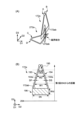
- FIG. 1 is a perspective view showing the configuration of a semiconductor module according to a first embodiment of the present invention.
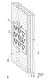
- FIG. 2 is a perspective view showing a plurality of inductors included in a logic chip and a group of inductors included in a plurality of memory chips according to a first embodiment of the present invention.
- 3(A) is a perspective view showing the configuration of the inductor on the logic chip and the inductor on the memory chip shown in FIG. 2
- FIG. 3(B) is a perspective view showing the structure of the inductor on the logic chip and the inductor on the memory chip shown in FIG.
- FIG. 1 is a block diagram showing the configuration of a semiconductor module according to a first embodiment of the present invention.
- FIG. 1 is a perspective view showing the configuration of a memory chip according to a first embodiment of the present invention. 6 is a cross-sectional view showing the cross-sectional structure of the memory chip taken along line A1-A2 shown in FIG. 5.
- FIG. FIG. 1 is a block diagram showing the configuration of a memory chip according to a first embodiment of the present invention.
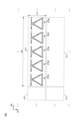
- FIG. 2 is a plan view showing the configuration of an inductor group included in the memory chip according to the first embodiment of the present invention.
- FIG. 1 is a perspective view showing the configuration of a logic chip according to a first embodiment of the present invention.
- 10 is a cross-sectional view showing the cross-sectional structure of the logic chip taken along the line B1-B2 shown in FIG. 9.
- FIG. 1 is a block diagram showing the configuration of a logic chip according to a first embodiment of the present invention.
- FIG. 2 is a plan view showing the configuration of an inductor group included in the logic chip according to the first embodiment of the present invention.
- 1 is a perspective view and a schematic diagram showing the configurations of an inductor included in a logic chip and an inductor included in a memory chip according to a first embodiment of the present invention.
- FIG. FIG. 3 is a schematic diagram showing the positional relationship of inductor groups included in each of a plurality of memory chips according to the first embodiment of the present invention.
- FIG. 2 is a schematic diagram showing the positional relationship of an inductor group included in the logic chip according to the first embodiment of the present invention.
- FIG. 2 is a schematic diagram showing the relationship between an inductor group included in a logic chip and a memory chip (an inductor group included in a memory chip) during inductor communication according to the first embodiment of the present invention.
- 17(A) to 17(C) are schematic diagrams showing a method for manufacturing a semiconductor module according to the first embodiment of the present invention.
- 18(A) to 18(C) are schematic diagrams showing a method for manufacturing a semiconductor module according to the first embodiment of the present invention.
- FIG. 2 is a schematic diagram showing the configuration of a semiconductor module according to a comparative example.
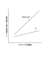
- 7 is a graph showing power and delay time during data communication with respect to the stacked number of memory chips in the semiconductor module according to the first embodiment of the present invention and the semiconductor module according to a comparative example.
- FIG. 7 is a schematic diagram showing the positional relationship of an inductor group included in a logic chip according to a second embodiment of the present invention.
- FIG. 7 is a schematic diagram showing the relationship between an inductor group included in a logic chip and a memory chip (an inductor group included in a memory chip) during inductor communication according to a second embodiment of the present invention.
- FIG. 7 is a schematic diagram showing the positional relationship of inductor groups included in each of a plurality of memory chips according to a second embodiment of the present invention.
- 24(A) and 24(B) are schematic diagrams showing a method for manufacturing a semiconductor module according to a second embodiment of the present invention.
- FIG. 1 is a schematic diagram showing the positional relationship of an inductor group included in a logic chip according to a second embodiment of the present invention.
- FIG. 7 is a schematic diagram showing the positional relationship of inductor groups included in each of a plurality of memory chips according to a third embodiment of the present invention.
- FIG. 7 is a schematic diagram showing the positional relationship of an inductor group included in a logic chip according to a third embodiment of the present invention.
- FIG. 7 is a schematic diagram showing the relationship between an inductor group included in a logic chip and a memory chip (an inductor group included in a memory chip) during inductor communication according to a third embodiment of the present invention.
- 28(A) to 28(D) are schematic diagrams showing a method for manufacturing a semiconductor module according to a third embodiment of the present invention.
- FIG. 29(A) and 29(B) are schematic diagrams showing a method for manufacturing a semiconductor module according to a third embodiment of the present invention.
- 30(A), FIG. 30(B), and FIG. 30(C) are schematic diagrams showing a method for manufacturing a semiconductor module according to a fourth embodiment of the present invention.
- 31(A) and 31(B) are schematic diagrams showing a method for manufacturing a semiconductor module according to a fourth embodiment of the present invention.
- FIG. 32(A) is a plan view showing the configuration of an inductor included in a seal ring and a memory chip according to the fifth embodiment of the present invention
- FIG. 32(B) is a plan view taken along line C1-C2 in FIG.
- FIG. 33(A) is a plan view showing the configuration of an inductor included in a seal ring and a logic chip according to the fifth embodiment of the present invention
- FIG. 33(B) is a plan view taken along the line J1-J2 in FIG. 33(A).
- FIG. 34(A) is a plan view showing the configuration of an inductor included in a seal ring and a memory chip according to the fifth embodiment of the present invention
- FIG. 34(B) is a plan view taken along the line E1-E2 in FIG. FIG.
- FIG. 35(A) is a plan view showing a method of manufacturing an inductor included in a memory cube according to the sixth embodiment of the present invention
- FIG. 35(B) is a side view showing a memory cube and an inductor included in the memory cube.
- FIG. 36(A) is a plan view showing a method for manufacturing an inductor included in a memory cube according to the sixth embodiment of the present invention
- FIG. 36(B) is a plan view taken along line F1-F2 in FIG. 35(A).
- FIG. 3 is a cross-sectional view showing a cross section of a memory cube.
- FIG. 37(A) is a plan view showing a method for manufacturing an inductor included in a memory cube according to the sixth embodiment of the present invention
- FIG. 37(B) is a side view showing a memory cube and an inductor included in the memory cube.
- FIG. 38(A) is a plan view showing a method for manufacturing an inductor included in a memory cube according to the sixth embodiment of the present invention
- FIG. 38(B) is a plan view taken along line G1-G2 in FIG. 37(A).
- FIG. 3 is a cross-sectional view showing a cross section of a memory cube.
- FIG. 7 is a perspective view showing the configuration of a power supply line of a semiconductor module according to a seventh embodiment of the present invention.
- FIG. 40 is a cross-sectional view showing a cross section of the semiconductor module taken along line H1-H2 in FIG. 39.
- 41(A) and 41(B) are side views showing a method for manufacturing a power supply line for a semiconductor module according to a seventh embodiment of the present invention.
- FIG. 7 is a perspective view showing an integrated circuit mounted with a semiconductor module according to an eighth embodiment of the present invention.
- FIG. 43 is a cross-sectional view showing a cross section of the integrated circuit of FIG. 42;
- FIGS. 44(A) to 44(C) are cross-sectional views showing a cross section of an integrated circuit mounted with a semiconductor module according to an eighth embodiment of the present invention. It is a flowchart which shows the mounting method of the semiconductor module based on 9th Embodiment of this invention.
- a member or region when referred to as being “above (or below)” another member or region, it is meant to be directly above (or below) the other member or region, unless otherwise specified. This includes not only the case where it is located directly below (directly below) but also the case where it is above (or below) another member or area, that is, another component is included in between above (or below) another member or area. Including cases.
- the D1 direction intersects the D2 direction
- the D3 direction intersects the D1 direction and the D2 direction (D1D2 plane).
- the D1 direction is called a first direction
- the D2 direction is called a second direction
- the D3 direction is called a third direction.
- the expressions “identical” and “identical” when the expressions “identical” and “identical” are used, the “identical” and “identical” may include errors within the design range. Furthermore, in an embodiment of the present invention, when an error is included in the design range, the expressions “substantially identical” and “substantially matched” may be used.
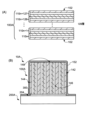
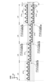
- FIG. 1 is a perspective view showing the configuration of a semiconductor module 10.
- FIG. 2 is a perspective view showing a plurality of inductors 272 included in the logic chip 200 and an inductor group 171 included in the plurality of memory chips 110.
- 3(A) is a perspective view showing the configuration of the inductor 272 on the logic chip 200 shown in FIG. 2 and the inductor 172 on the memory chip 110
- FIG. 5 is a diagram showing the positional relationship with an inductor 172 on the memory chip 110.
- FIG. FIG. 4 is a block diagram showing the configuration of the semiconductor module 10.
- the semiconductor module 10 includes a memory cube 100, a logic chip 200, and an adhesive layer 300.
- Logic chip 200 is sometimes called a semiconductor chip.
- the memory cube 100 includes a structure in which a plurality of memory chips 110 are stacked, and is arranged on the second surface 204 of the logic chip 200.
- Each of the plurality of memory chips 110 includes a similar configuration.
- Each of the plurality of memory chips 110 includes, for example, a transistor layer 130, a wiring layer 150, and an inductor layer 170.
- the logic chip 200 includes, for example, a transistor layer 230, a wiring layer 250, and an inductor layer 270, and has a first surface 202 parallel to a D1 direction (first direction) and a D2 direction (second direction) that intersects the first direction. , including a first surface 202 and an opposite second surface 204.
- the first surface 202 is a surface opposite to the surface on which the wiring layer 250 is arranged with respect to the transistor layer 230
- the second surface 204 is the surface on the opposite side to the surface on which the wiring layer 250 is arranged with respect to the inductor layer 270. It is a surface.
- Adhesive layer 300 is disposed between second side 146 of memory cube 100 and second side 204 of logic chip 200 and connects memory cube 100 and logic chip 200.
- the inductor layer 170 of each of the plurality of memory chips 110 is arranged in a D3 direction (third direction) perpendicular to the first direction and the second direction (i.e., the first surface 202 and the second surface 204).
- the first inductor includes a plurality of inductors 172 (first inductors) arranged in parallel with each other.
- the logic chip 200 includes a plurality of inductors 272 (second inductors) arranged parallel to the positions where the plurality of inductors 172 are arranged and parallel to and close to the second surface 204 .
- the inductor layer 270 includes a plurality of inductors 272.
- the plurality of memory chips 110 include, for example, a memory chip 110n and a memory chip 110n+1 arranged adjacent to the memory chip 110n.
- Memory chip 110n includes an inductor layer 170n.
- the inductor layer 170n includes a plurality of inductors 172, and the plurality of inductors 172 includes an inductor 172b including one linear side 172bb.
- the memory chip 110n+1 includes an inductor layer 170n+1.
- the inductor layer 170n+1 includes a plurality of inductors 172, and the plurality of inductors 172 includes an inductor 172a including one linear side 172ab. Note that, like the inductors 172b and 172a, one straight side 172bb and one straight side 172ab are close to and parallel to the second surface 204.
- the plurality of inductors 172 are arranged in parallel in the second direction.
- Inductor 172 includes terminal A and terminal B. Although details will be described later, the inductor 172 is electrically connected to the transmitting/receiving circuit 114 using terminals A and B.
- the plurality of inductors 272 are arranged in a matrix in the first direction and the second direction.
- the plurality of inductors 272 include an inductor 272a including one linear side 272ab, and an inductor 272b including one linear side 272bb.
- Inductor 272 includes terminal C and terminal D. Although details will be described later, the inductor 272 is electrically connected to the transmitting/receiving circuit 214 using terminals C and D.
- the shape of the inductor 172 and the shape of the inductor 272 are, for example, triangular. Since the memory chip 110 stands perpendicular to the logic chip 200, the inductor 172 faces the inductor 272 at 90 degrees. Among the plurality of inductors 172 and the plurality of inductors 272, one inductor 172 and one inductor 272 facing each other are magnetically coupled to each other, so that the inductors can communicate with each other on a one-to-one basis. Communication between inductors associated with magnetic field coupling is called, for example, inductor communication, signal communication, data communication, or the like.
- the shape of the inductor 172 and the shape of the inductor 272 are not limited to the triangular shape.
- the shape of the inductor 172 and the shape of the inductor 272 may be trapezoidal or pentagonal.
- the shape of the inductor 172 and the shape of the inductor 272 may be any shape that allows inductor communication.
- inductor 172a and inductor 272a face each other at 90 degrees, and can communicate one-to-one by magnetic field coupling. More specifically, effective inductor communication is performed by the base of the triangle of inductor 172a (one straight side 172ab) and the base of the triangle of inductor 272a overlapping with one straight side 172ab (one straight side 272ab).
- One straight side 172ab mainly has the function of performing inductor communication with one straight side 272ab.
- the two sides other than one straight side 172ab mainly have the function of supplying current to one straight side 172ab.
- inductor 272a Similar to inductor 172a, in inductor 272a, the two sides other than one straight side 272ab mainly have the function of supplying current to one straight side 272ab. Inductor 172b and inductor 272b have the same configuration and function as inductor 172a and inductor 272a.
- each of the plurality of inductors 172 includes a first side 193a, extends in the D3 direction, and has a first width DS that is limited in the D2 direction.
- a second portion 194 including a second side 194a and extending in the D3 direction and having a finite second width DS in the D2 direction;
- the third portion 196 includes one linear side (for example, side 172ab), extends in the D2 direction, has a length Dh parallel to the D22 direction, and has a finite third width Wid in the D3 direction.
- the distances (distance W1, distance W2, and distance W3) between the first side 193a and the second side 194a cut parallel to the second surface 204 are the same as the distances (distance W1, distance W2, and distance W3) that are The distance from the second surface 204 becomes shorter. That is, distance W1, distance W2, and distance W3 become shorter in this order.
- the inductor 172a is arranged perpendicularly to the second side surface 146 of the memory cube 100.
- the first side 193a and the second side 194a are defined as lines extending in the D3 direction and D2 direction, and one linear side (for example, 172ab) is defined as a side extending in the D2 direction.
- the shape of the region 195 formed by is triangular. Note that the shape of the region 195 is not limited to a triangular shape.
- the inductor 172a has a fourth part (not shown) including a third side (not shown) between the first side 193a and one straight side, and a fourth part (not shown) that is straight with the second side 194a.
- the region 195 may have a trapezoidal shape including a fifth portion (not shown) including a fourth side (not shown) between one side of the shape, or a pentagonal shape.
- the shape may be a pentagonal shape.
- the shape of the inductor 172a and the shape of the region 195 may be any shape that allows inductor communication.
- Inductor 272a may have a similar configuration and function as inductor 172a. Note that in this specification and the drawings, viewing a plane parallel to the D2 direction and the D3 direction from the D1 direction is referred to as a front view.
- the memory cube 100 includes a plurality of magnetically coupled chip interfaces (Through Chip Interface-IO (TCI-IO)) 112 and a plurality of memory modules 111.
- TCI-IO Through Chip Interface-IO
- the plurality of TCI-IOs 112 are electrically connected to the memory module 111.
- the TCI-IO 112 includes an inductor 172, a transmission/reception circuit 114, and a parallel-to-serial conversion circuit 113.
- Inductor 172 is electrically connected to transmitter/receiver circuit 114 using terminals A and B.
- the transmitter/receiver circuit 114 is electrically connected to the parallel-serial converter circuit 113 .
- Parallel-to-serial conversion circuit 113 is electrically connected to memory module 111 .
- the inductor 172 has a function of contactless inductor communication with the inductor 272 of the logic chip 200.
- the transmitting/receiving circuit 114 has, for example, a function of amplifying the signal (data) received by the inductor 172 and a function of removing noise from the received signal (data). Further, the transmitting/receiving circuit 114 has a function of transmitting, for example, a desired signal (data) converted using the parallel-to-serial converting circuit 113 onto radio waves.
- the signal received by inductor 172 includes multiple parallel signals from logic chip 200.
- the desired signals include multiple parallel signals from memory module 111.
- step 1 the parallel-to-serial conversion circuit 113 performs parallel-to-serial conversion on a large number of parallel signals from the logic chip 200 to convert them into a serial signal (serial signal). Serial signals are transferred at high speed using one signal path (wiring).
- step 2 the parallel-to-serial conversion circuit 113 performs serial-to-parallel conversion on the serial signal immediately before the memory module 111, returns it to a large number of parallel signals, and then transmits the large number of parallel signals to the memory module 111. .
- the parallel-to-serial conversion circuit 113 executes step 1 following step 2, for example.
- the parallel-to-serial conversion circuit 113 is called, for example, a SerDes circuit (Serialize and Deserialize Circuit).
- the memory module 111 includes, for example, a function of generating a large number of parallel signals to be transmitted, and a function of controlling a large number of received parallel signals and storing them in the memory cell array 115 (see FIG. 7).
- the logic chip 200 includes a plurality of magnetic field coupling chip interfaces (Through Chip Interface-IO (TCI-IO)) 212 and a plurality of logic modules 211.
- TCI-IO Through Chip Interface-IO
- the plurality of TCI-IOs 212 are electrically connected to the logic module 211.
- the TCI-IO 212 includes an inductor 272, a transmission/reception circuit 214, and a parallel-to-serial conversion circuit 213.
- Inductor 272 is electrically connected to transmitter/receiver circuit 214 using terminals C and D.
- the transmitter/receiver circuit 214 is electrically connected to the parallel-to-serial converter circuit 213 .
- Parallel-serial conversion circuit 213 is electrically connected to logic module 211 .
- the configurations and functions of the inductor 272, the transmission/reception circuit 214, the parallel-serial conversion circuit 213, and the logic module 211 are the same as those of the inductor 172, the transmission/reception circuit 114, the parallel-serial conversion circuit 113, and the memory module 111. Therefore, descriptions of the configurations and functions of the inductor 272, the transmission/reception circuit 214, the parallel-to-serial conversion circuit 213, and the logic module 211 will be omitted here.
- the semiconductor module 10 includes the functions and configurations described above. Signals are transmitted and received between the inductor 172 included in the memory chip 110 and the inductor 272 included in the logic chip 200 using non-contact inductor communication.
- the distance between the memory chip 110 (inductor 172) and the logic chip 200 (inductor 272) in the semiconductor module 10 is substantially the thickness of the adhesive layer 300.
- the distance between the memory chip 110 (inductor 172) and the logic chip 200 (inductor 272) in the semiconductor module 10 is the distance between the memory chip 110 and the logic chip 200 that are connected using wiring, through electrodes, bumps, etc.
- the memory chip 110 and the logic chip 200 can be bonded to each other using the thin adhesive layer 300 without creating a gap due to the bumps, so that the thermal resistance is low and the heat dissipation characteristics are excellent. Further, since the wiring resistance and parasitic capacitance of the semiconductor module 10 are suppressed, power consumption in communication using the semiconductor module 10 can be suppressed.
- the semiconductor module 10 includes a memory cube 100 in which a plurality of memory chips 110 including a plurality of inductors 172 are stacked, and a large-capacity memory can be realized without increasing the size of the memory chip. That is, the semiconductor module 10 includes a large-capacity memory in which wiring resistance and parasitic capacitance of the semiconductor module 10 are suppressed compared to a module having a large chip size. Therefore, a memory with low power consumption and large capacity can be realized by using the semiconductor module 10.
- the semiconductor module 10 includes a configuration in which one-to-one inductor communication is possible between the inductor 172 and the inductor 272, which are arranged to face each other at 90 degrees. Further, a plurality of inductors 172 are arranged in parallel to the second side surface 146 of the memory cube 100, a plurality of inductors 272 are arranged in parallel to the second surface 204 of the logic chip 200, and the inductors communicate with each other on a one-to-one basis. be able to. As a result, it is easy to communicate large amounts of signals (data) in parallel.
- the semiconductor module 10 includes, for example, a plurality of triangular inductors 172, and the distance between the two sides of the inductor 172 becomes shorter as the distance from the second surface 204 increases. That is, the distance between two adjacent inductors 172 increases as the distance from the second surface 204 increases. Therefore, since two adjacent inductors 172 are unlikely to interfere with each other, the semiconductor module 10 can suppress crosstalk.
- FIG. 5 is a perspective view showing the configuration of the memory chip 110.
- FIG. 6 is a cross-sectional view showing the cross-sectional structure of the memory chip 110 along line A1-A2 shown in FIG.
- FIG. 7 is a block diagram showing the configuration of the memory chip 110.
- FIG. 8 is a plan view showing the configuration of the inductor group 171. Descriptions of configurations that are the same or similar to those in FIGS. 1 to 4 will be omitted here.
- the memory cube 100 includes a configuration in which a plurality of memory chips 110 are stacked in the D1 direction.
- the memory cube 100 includes a first surface 142 parallel to the D2 direction and the D3 direction, and a second surface 144 opposite to the first surface 142 and parallel to the first surface 142 with respect to the D1 direction.
- the memory cube 100 also includes a first side surface 145 perpendicular to the first surface 142 and the second surface 144, a second side surface 146 adjacent to the first side surface 145, a third side surface 147 adjacent to the second side surface 146, and It includes a third side 147 and a fourth side 148 adjacent to the first side 145 .
- the second side surface 146 is in contact with the adhesive layer 300, and the memory cube 100 is placed on the second surface 204 of the logic chip 200.
- each of the plurality of memory chips 110 includes, for example, a transistor layer 130, a wiring layer 150, and an inductor layer 170.
- Each of the plurality of memory chips 110 includes, for example, a memory chip 110n, a memory chip 110n+1 adjacent to the memory chip 110n, a memory chip 110n+2 adjacent to the memory chip 110n+1, a memory chip 110n+3 adjacent to the memory chip 110n+2, and a memory chip 110n+3 adjacent to the memory chip 110n+3.
- the memory chip 110n+4 includes a memory chip 110n+4.
- the memory chip is expressed as a memory chip 110.
- the memory chips are expressed as a memory chip 110n, a memory chip 110n+1, a memory chip 110n+2, etc.
- the inductor group is expressed as an inductor group 171
- the inductor is expressed as an inductor 172.
- the inductor groups 171a, 171b, etc. are expressed as inductor groups 171a, 171b, etc.
- the inductors are expressed as inductors 172a, 172b, etc.
- the memory chip 110 includes a first surface 102 parallel to the D2 direction and the D3 direction, and a second surface 104 opposite to the first surface 102 with respect to the D1 direction.
- the first surface 102 is a surface opposite to the transistor layer 130 on which the wiring layer 150 is disposed
- the second surface 104 is the surface opposite to the surface on which the wiring layer 250 is disposed relative to the inductor layer 170. It is a surface.
- the first surface 102 and the second surface 104 are parallel to the first surface 142 and the second surface 144.
- the memory chip 110 also has a first side surface 105 perpendicular to the first surface 102 and the second surface 104, a second side surface 106 adjacent to the first side surface 105, a third side surface 107 adjacent to the second side surface 106, and It includes a third side 107 and a fourth side 108 adjacent to the first side 105 .
- the first side 105 is a part of the first side 145
- the second side 106 is a part of the second side 146
- the third side 107 is a part of the third side 147
- the fourth side 108 is a part of the second side 145. It is a part of the fourth side surface 148.
- the inductor layer 170 includes a plurality of inductor groups 171.
- Each of the plurality of inductor groups 171 includes a plurality of inductors 172.
- inductor group 171 includes five inductors 172.
- the plurality of inductor groups 171 include a plurality of inductors 172 arranged perpendicularly to the D2 direction and the D3 direction (that is, the first surface 102 and the second surface 104) and parallel to the D3 direction.
- Each of the plurality of inductor groups 171 is arranged apart from the fourth side surface 108 and close to the second side surface 146, and is arranged to extend in the D2 direction.
- the number of the plurality of inductors 172 included in the inductor group 171 is not limited to five. The number of inductors 172 can be changed as appropriate depending on the specifications, usage, etc. of the semiconductor module 10.
- the transistor layer 130 includes, for example, a substrate 173, an element isolation region 174, an activation region 175, a transistor 176, an insulating layer 177, and a portion of a wiring 178.
- the substrate 173 is, for example, a Si substrate or a Si-wafer.
- the wiring layer 150 includes a multilayer wiring structure in which wiring and insulating layers are alternately stacked.
- the wiring layer 150 includes, for example, a part of the wiring 178, an insulating layer 179, a wiring 180, and an insulating layer 181.
- the number of layers of multilayer wiring in wiring layer 150 is not limited to two layers shown in FIG. 6 .
- the number of multilayer wiring layers in the wiring layer 150 may be three or more layers.
- the number of multilayer wiring layers in the wiring layer 150 can be changed as appropriate depending on the specifications, usage, etc. of the semiconductor module 10.
- the inductor layer 170 includes, for example, an insulating layer 182 and a plurality of inductors 172. Further, the inductor layer 170 includes a plurality of inductor groups 171.
- the memory chip 110 includes a plurality of memory modules 111, a plurality of TCI-IOs 112, a power supply wiring 164, and a ground wiring 165.
- Each of the plurality of memory modules 111 includes a memory cell array 115.
- Each of the plurality of TCI-IOs 112 includes a plurality of inductor groups 171, and the inductor group 171 includes a plurality of inductors 172.
- the memory module 111 stores signals (data) in the memory cell array 115, reads signals (data) from the memory cell array 115, transmits signals (data) to the TCI-IO 112, or reads signals (data) from the TCI-IO 112. It has a function to control the reception of data).
- the memory cell array 115 includes a plurality of memory cells (not shown).
- Each of the plurality of memory cell arrays 115 is, for example, an SRAM (Static Random Access Memory), and each of the plurality of memory cells is an SRAM cell. It is a cell.
- the SRAM, the SRAM cell, and the memory module 111 for SRAM can employ technology used in the technical field of SRAM. Therefore, detailed explanation will be omitted here.
- the plurality of memory cell arrays 115 and the plurality of memory cells may be memory cell arrays and memory cells other than SRAM, such as DRAM (Dynamic Random Access Memory), DRAM cells, and MRAM (Magnetoresistive Random Access Memory). Memory) and MRAM cell etc.
- the plurality of memory modules 111 and the plurality of TCI-IOs 112 are electrically connected to a power supply wiring 164 and a ground wiring 165.
- the power supply wiring 164 and the ground wiring 165 are electrically connected to, for example, an external circuit (not shown), and are supplied with power (VDD), VSS, and the like.
- VDD is, for example, 1V or 3V.
- VSS is, for example, a ground voltage, 0V, or the like.
- the plurality of inductor groups 171 are close to the second side surface 106 of the memory chip 110 and are arranged in parallel in the D2 direction.
- Each of the plurality of inductor groups 171 includes a plurality of inductors 172.
- inductor group 171 includes five inductors 172c, 172d, 172e, 172f, and 172g.
- the plurality of inductors 172 include, for example, an inductor having a data communication (data transmission) function and an inductor having a clock communication (clock transmission) function.
- the inductor group 171 is sometimes called a channel.
- the inductor 172c has a function of data communication with the inductor 272 with a one-to-one correspondence, and is called a first data channel (Data Channel 1).
- Inductors 172d, 172f, and 172g have the same function and configuration as inductor 172c, and are connected to the second data channel (Data Channel 2), the third data channel (Data Channel 3), and the fourth data channel (Data Channel 3), respectively. 4) It is called.
- the inductor 172e has a function of clock communication (clock transmission) with the inductor 272 with one-to-one correspondence, and is called a clock channel.
- Each inductor 172 may perform inductor communication with the corresponding inductor 272 on a one-to-one basis (in synchronization) with the clock received through clock communication. (asynchronously), inductor communication may be performed with one-to-one corresponding inductor 272. Further, for example, the inductor 172e does not have a clock communication function and has the same function and configuration as the inductor 172c, and each inductor 172 performs inductor communication with the corresponding inductor 272 on a one-to-one basis in an asynchronous manner. Good too.
- the inductor communication of the semiconductor module 10 can be selected as appropriate based on the specifications, usage, etc. of the semiconductor module 10 without departing from the scope of the present invention.
- the length MCBZ (see FIG. 1) of the memory cube 100 in the D1 direction is 5.12 mm
- the length MCBY (see FIG. 1) of the memory cube 100 in the D2 direction is 5.00 mm
- the length MCBZ (see FIG. 1) of the memory cube 100 in the D3 direction is 5.12 mm
- the length MCBX (see Figure 1) is 5.00 mm.
- the thickness THI (see FIG. 6) of the memory chip 110 is 80 ⁇ m.
- the length MIX (see FIG. 8) of the inductor group 171 parallel to the D2 direction is 600 ⁇ m
- the length MIY (see FIG. 8) of the inductor group 171 parallel to the D3 direction is 160 ⁇ m.
- the memory chip 110 is manufactured using a 2 nm CMOS process
- the memory cube 100 is configured with the above size in which 64 memory chips 110 are stacked
- the inductor group 171 is configured with the above size including four data channels.
- the data transfer rate is 200 Gbps.
- the data rate of one data channel of the inductor 172 and the inductor 272 is 50 Gbps
- the frequency of the system clock of the clock channel is 0.5 GHz
- the clock frequency of the transmitting/receiving circuits 114 and 214 is 250 GHz.
- FIG. 9 is a perspective view showing the configuration of the logic chip 200.
- FIG. 10 is a cross-sectional view showing the cross-sectional structure of the logic chip 200 taken along the line B1-B2 shown in FIG.
- FIG. 11 is a block diagram showing the configuration of the logic chip 200.
- FIG. 12 is a plan view showing the configuration of the inductor group 271. Descriptions of configurations that are the same or similar to those in FIGS. 1 to 8 will be omitted here.
- the semiconductor module 10 includes a first surface 202 parallel to the D1 direction and the D2 direction, and a second surface 204 opposite to the first surface 202.
- the first surface 202 is a surface opposite to the surface on which the wiring layer 250 is arranged with respect to the transistor layer 230
- the second surface 204 is the surface on the opposite side to the surface on which the wiring layer 250 is arranged with respect to the inductor layer 270. It is a surface.
- the logic chip 200 includes, for example, a transistor layer 230, a wiring layer 250, and an inductor layer 270.
- the inductor layer 170 includes a plurality of inductor groups 271.
- Each of the plurality of inductor groups 271 includes a plurality of inductors 272.
- inductor group 271 includes five inductors 272.
- the plurality of inductor groups 271 are arranged in a matrix in parallel to the D1 direction and the D2 direction (that is, the first surface 202 and the second surface 204).
- the plurality of inductors 172 are arranged in a matrix in parallel to the D1 direction and the D2 direction (that is, the first surface 202 and the second surface 204).
- the number of the plurality of inductors 272 included in the inductor group 271 is not limited to five. The number of inductors 272 can be changed as appropriate depending on the specifications, usage, etc. of the semiconductor module 10.
- the logic chip 200 includes a memory cube placement area 210 approximately in the center.
- the memory cube arrangement area 210 is in contact with the adhesive layer 300, and the adhesive layer 300 is arranged thereon.
- the memory cube 100 is placed on the memory cube placement area 210.
- the memory cube arrangement area 210 overlaps the plurality of inductor groups 271.
- the plurality of inductor groups 271 are arranged inside the memory cube arrangement area 210 when viewed from the front.
- the inductor group is expressed as an inductor group 271 and the inductor is expressed as an inductor 272.
- the inductor groups are expressed as inductor groups 271a, 271b, etc.
- the inductors are expressed as inductors 272a, 272b, etc.
- the transistor layer 230 includes, for example, a substrate 273 including an element isolation region 274 and an activation region 275, a transistor 276a, a transistor 276b, an insulating layer 277, a part of a wiring 278a, and a part of a wiring 278b.
- the substrate 273 is, for example, a Si substrate or a Si-wafer.
- the wiring layer 250 includes a multilayer wiring structure in which wiring and insulating layers are alternately stacked.
- the wiring layer 250 includes, for example, a part of the wiring 278a, a part of the wiring 278b, an insulating layer 279, a wiring 280a, a wiring 280b, and an insulating layer 281.
- the number of layers of multilayer wiring in wiring layer 250 is not limited to two layers shown in FIG. 10.
- the number of layers of multilayer wiring in the wiring layer 250 may be three or more layers.
- the number of multilayer wiring layers in the wiring layer 250 can be changed as appropriate depending on the specifications, usage, etc. of the semiconductor module 10.
- the inductor layer 270 includes, for example, an insulating layer 282 and a plurality of inductors 272 (inductor 272a, inductor 272b). Further, the inductor layer 270 includes a plurality of inductor groups 271.
- the logic chip 200 includes, for example, a plurality of logic modules 211, a plurality of TCI-IOs 212, a plurality of DRAM interfaces (Dynamic Random Access Memory (DRAM) IO) 215, and a plurality of external IOs 216.
- Each of the plurality of TCI-IOs 212 includes a plurality of inductor groups 271, and the inductor group 271 includes a plurality of inductors 272.
- the configuration of the logic chip 200 shown in FIG. 11 is an example, and the configuration of the logic chip 200 is not limited to the example shown in FIG. 11.
- logic chip 200 may not include DRAMIO 215.
- the logic module 211 has a function for controlling the transmission of signals (data) to the TCI-IO 212 or the reception of signals (data) from the TCI-IO 212. Furthermore, the logic module 211 has a function of driving the memory module 111 within the memory chip 110. For example, the logic module 211 transmits a signal for driving the memory module 111 via the TCI-IO 212.
- the logic module 211 may include, for example, an arithmetic circuit such as a CPU (Central Processing Unit).
- the DRAMIO 215 is electrically connected to, for example, the DRAM module 400 (see FIG. 42), and has a function of transmitting and receiving signals between the DRAM module 400 and the logic chip 200.
- the external IO 216 is electrically connected to, for example, the logic chip 200 and an external circuit (not shown, such as a power supply circuit), and has a function of transmitting and receiving signals between the external circuit and the logic chip 200.
- Each of the plurality of logic modules 211 is electrically connected to a part of the plurality of TCI-IOs 212, a part of the plurality of DRAMIOs 215, and a part of the plurality of external IOs.
- Each of the plurality of logic modules 211 is supplied with power (VDD), VSS, etc. from an external circuit, receives a control program stored in the DRAM module 400 from the DRAM module 400, and executes processing of the control program. .
- the plurality of inductor groups 271 are arranged in a matrix in the D1 direction and the D2 direction.
- Each of the plurality of inductor groups 271 includes a plurality of inductors 272.
- inductor group 271 includes five inductors 272c, 272d, 272e, 272f, and 272g.
- the plurality of inductors 272, like the plurality of inductors 172 include, for example, an inductor having a data communication (data transmission) function and an inductor having a clock communication (clock transmission) function.
- the inductor group 271, like the inductor group 171 is sometimes called a channel.
- the inductor 272c has a function of data communication with the inductor 172 with one-to-one correspondence, and the first data channel ( It is called Data Channel 1).
- the inductors 272d, 272f, and 272g have the same function and configuration as the inductor 272c, and are connected to the second data channel (Data Channel 2), the third data channel (Data Channel 3), and the fourth data channel (Data Channel 3), respectively. 4) It is called.
- the inductor 272e has a function of clock communication (clock transmission) with the inductor 172 with one-to-one correspondence, and is called a clock channel.
- each inductor 272 may perform inductor communication with the corresponding inductor 172 on a one-to-one basis in response to (synchronized with) the clock received through clock communication; Inductor communication may be performed with one-to-one corresponding inductor 172 without synchronization (asynchronously).
- the inductor 272e does not have a clock communication function and has the same function and configuration as the inductor 272c, and each inductor 272 performs inductor communication with the corresponding inductor 172 on a one-to-one basis in an asynchronous manner. Good too.
- the length LCX (see FIG. 1) of the logic chip 200 in the D1 direction is 12.00 mm
- the length LCY (see FIG. 1) of the logic chip 200 in the D2 direction is 12.00 mm
- the thickness of the logic chip 200 in the D3 direction is 80 ⁇ m, similar to the thickness THI of the memory chip 110 (see FIG. 1).
- the length LIX (see FIG. 12) of the inductor group 271 parallel to the D2 direction is 600 ⁇ m
- the length LIY (see FIG. 12) of the inductor group 271 parallel to the D1 direction is 160 ⁇ m.
- the logic chip 200 is manufactured using a 2 nm CMOS process, and the inductor group 271 has the above size including four data channels. Further, the data transfer rate, the data rate of one data channel, the frequency of the system clock, and the clock frequencies of the transmitting/receiving circuits 114 and 214 are as described in "1-2. Overview of the memory cube 100."
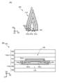
- FIG. 13 is a perspective view and a schematic diagram showing the configurations of an inductor 272 included in the logic chip 200 and an inductor 172 included in the memory chip 110. Descriptions of configurations that are the same or similar to those in FIGS. 1 to 12 will be omitted here.
- the perspective view of the inductor 172a and the inductor 272a shown in FIG. 13 is an enlarged view with a part of FIG. 2 omitted.
- the plurality of inductors 172 include the inductor 172a including one linear side 172ab, and the plurality of inductors 272 include one linear side 272ab.
- Inductor 272a is included.
- the inductor 172a and the inductor 272a are arranged to face each other at 90 degrees, and one straight side 172ab and one straight side 272ab are close to each other and parallel to each other, and are also parallel to the second surface 204. parallel.
- the plan view of the inductor 172a and the inductor 272a shown in FIG. is shown.
- the memory chip 110 is arranged in the D3 direction (that is, vertically installed) with respect to the second surface 204 of the logic chip 200, the inductor 172a and the inductor 272a are connected to the second surface 204 of the logic chip 200. In contrast, it is arranged in the D3 direction.
- the distance between the inductor 172a and the inductor 272a, and the distance between one straight side 172ab and one straight side 272ab are indicated by a distance Dis.
- the height of the inductor 172a is indicated by height MIDv
- the width of one linear side 172ab in the D3 direction is indicated by width Wid
- the length of the inductor 272a is indicated by the length Dh
- the height of the inductor 272a is indicated by the height LIDv.
- the interval (distance between) the inductors 172 adjacent to each other and the interval (distance between the inductors 272) adjacent to each other are indicated by the interval (distance) Sh.
- the distance Dis is 10 ⁇ m ⁇ 5 ⁇ m (3 ⁇ ), for example, 18 ⁇ m.
- the height MIDv is, for example, 160 ⁇ m
- the width Wid is, for example, 20 ⁇ m
- the length Dh is, for example, 80 ⁇ m
- the height LIDv is, for example, 80 ⁇ m.
- the length Dh may be, for example, four times or more the distance Dis, and may be four times or more the distance Dis and 15 times or less the distance Dis.
- the height MIDv may be, for example, greater than or equal to the length Dh, and may be greater than or equal to the length Dh and less than or equal to 5 times the length Dh.
- the distance Sh may be, for example, 1/4 or more of the length Dh, 1/2 or more of the length Dh, and 2 times or less of the length Dh.
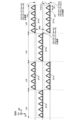
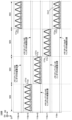
- FIG. 14 is a schematic diagram showing the positional relationship of the inductor groups 171 included in each of the plurality of memory chips 110
- FIG. 15 is a schematic diagram showing the positional relationship of the plurality of inductor groups 271
- FIG. 16 is a schematic diagram showing the positional relationship of the plurality of inductor groups 271.
- FIG. 2 is a schematic diagram showing the relationship between an inductor group 271 included in a logic chip 200 and a memory chip 110 (an inductor group 171 included in a memory chip 110). Descriptions of configurations that are the same or similar to those in FIGS. 1 to 13 will be omitted here.
- the memory cube 100 includes memory chips 110n to 110n+3, for example, as described in "1-2. Overview of the memory cube 100."
- the memory chip 110n and the memory chip 110n+1 are stacked, for example, so that their inductor layers 170 (see FIG. 1) face each other, and the memory chip 110n+2 and the memory chip 110n+3 are stacked, for example, so that their inductor layers 170 (see FIG. 1) face each other. are stacked so that they are facing each other.
- the memory chip 110n+1 and the memory chip 110n+2 are stacked, for example, so that their transistor layers 130 (see FIG. 1) face each other.
- the inductor groups 171a to 171f shown in FIG. It is shown as follows. Actually, since the memory chips 110n to 110n+3 are arranged (vertical) in the D3 direction with respect to the second surface 204 of the logic chip 200, the inductor groups 171a to 171f are arranged on the second surface 204 of the logic chip 200. It is installed vertically.
- the memory chip 110n includes an inductor group 171b
- the memory chip 110n+1 includes an inductor group 171a and an inductor group 171c
- the memory chip 110n+2 includes an inductor group 171e
- the memory chip 110n+3 includes an inductor group 171d and an inductor group 171f.
- FIG. 14 is an enlarged view of a part of the memory cube 100, and each of the memory chips 110n to 110n+3 includes a plurality of inductor groups 171, and the plurality of inductor groups 171 are arranged apart from each other by a length MIX.
- the inductor group 171a is arranged a length MIX apart from the inductor group 171 adjacent in parallel in the D2 direction (not shown).
- the other inductor groups are arranged a length MIX apart from the inductor group 171 adjacent in parallel in the D2 direction (not shown).
- each of the inductor groups 171a to 171f includes the same configuration and function as the inductor group 171 described with reference to FIG. 8 in "1-2. Overview of the memory cube 100."
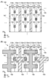
- the inductor groups 171a to 171f included in the memory chips 110n to 110n+3 are arranged in a checkered pattern. be done.
- the multiple inductor groups 271 include inductor groups 271a to 271f.
- the inductor groups 271a to 271f are uniformly arranged in a matrix in the D1 and D2 directions.
- Each of the inductor groups 271a to 271f includes the same configuration and function as the inductor group 271 described with reference to FIG. 12 in "1-3. Overview of the logic chip 200".
- One linear side (for example, 272ab) of each of the inductor groups 271a, 271b, and 271c is arranged in parallel, for example, on the boundary between the memory chip 110n and the memory chip 110n+1. Further, one linear side (for example, 272bb) of each of the inductor groups 271d, 271e, and 271f is arranged in parallel, for example, on the boundary between the memory chip 110n+2 and the memory chip 110n+3.
- the thickness THI of the memory chips 110n to 110n+3 and the logic chip 200 is 80 ⁇ m
- the interval between the boundary between the memory chip 110n and the memory chip 110n+1 and the boundary between the memory chip 110n+2 and the memory chip 110n+3 (distance between them) is 160 ⁇ m, which is twice the thickness THI (THI ⁇ 2).
- the length Dh is, for example, 70 ⁇ m
- the interval MIS (distance MIS) between the inductor group 271a and the inductor group 271d in the D1 direction is, for example, 90 ⁇ m. Therefore, in the semiconductor module 10 according to the first embodiment, the thickness THI of the memory chips 110n to 110n+3 and the logic chip 200 is thicker (longer) than the length Dh of one linear side of the inductor 172 and the inductor 272.
- the semiconductor module 10 includes three channels (Channel 1, Channel 2, and Channel 3).
- memory chip 110n and memory chip 110n+2 correspond to an even channel (channel 2)
- memory chip 110n+1 and memory chip 110n+3 correspond to odd channels (channel 1 and channel 3).
- the plurality of inductors 272 of the inductor group 271b included in the logic chip 200 communicate with the plurality of inductors 172 of the inductor group 171b included in the memory chip 110n in one-to-one correspondence through channel 2.
- the plurality of inductors 272 of the inductor group 271a each communicate with the plurality of inductors 172 of the inductor group 171a in one-to-one correspondence through channel 1, and the plurality of inductors 272 of the inductor group 271c each correspond one-to-one.
- the plurality of inductors 272 of the inductor group 271e communicate with the plurality of inductors 172 of the inductor group 171e corresponding one-to-one through channel 2, and the inductor group 271d communicates with the plurality of inductors 172 of the inductor group 171c.
- the plurality of inductors 272 communicate with the plurality of inductors 172 of the inductor group 171d that correspond to each other on a one-to-one basis
- the plurality of inductors 272 of the inductor group 271f communicate with the plurality of inductors 172 of the inductor group 171f that correspond to each other on a one-to-one basis. communicates with the inductor 172 on channel 3.
- the semiconductor module 10 can suppress crosstalk in communication between the logic chip 200 and the memory chip 110n and memory chip 110n+1, which are arranged at substantially the same position. Similarly, crosstalk in communication between the logic chip 200 and the memory chip 110n+2 and the memory chip 110n+3, which are arranged at substantially the same position, can be suppressed.
- the distance MIS between the inductor group 271a and the inductor group 271d in the D1 direction should be approximately the same length as the length Dh of one linear side of the inductor 172 and the inductor 272. is preferred. Thereby, crosstalk in communication between mutually adjacent inductors can be suppressed.
- the inductor Cm1 included in the inductor group 171a of the memory chip 110n+1 is magnetically coupled with the inductor Cl1 included in the inductor group 271a of the logic chip 200, so that inductor communication is possible.
- There is no magnetic field coupling with the inductor Cl4 included in the inductor and there is no crosstalk.
- the inductor Cl1 and the inductor Cl4 are not magnetically coupled and do not have crosstalk.
- FIGS. 17 and 18 are schematic diagrams showing a method of manufacturing the semiconductor module 10. Descriptions of configurations that are the same or similar to those in FIGS. 1 to 16 will be omitted here.
- the stacking (bonding) of memory chips 110 such that their second surfaces 104 on the inductor layer 170 side face each other is called, for example, F2F bonding (Face to Face Fusion).
- the stacking (bonding) of the memory chips 110 such that their first surfaces 102 on the transistor layer 130 side face each other is called, for example, B2B bonding (Back to Back Fusion).
- the stacking (bonding) of the memory chips 110 such that the second surface 104 on the inductor layer 170 side and the first surface 102 on the transistor layer 130 side face each other is called, for example, F2B bonding (Face to Back Fusion).
- the stacking (bonding) of memory chips can be performed using, for example, a technique such as welding (Fusion Bonding) or Silicon Direct Bonding (SDB). Since this is a technique used in the field, a detailed explanation will be omitted here.
- step 1 the second surface 104 of the memory chip 110n and the second surface 104 of the memory chip 110n+1 are stacked (bonded) so as to face each other (see FIG. 17(A)). That is, in step 1, the two memory chips 110n and 110n+1 are joined by F2F junction.
- the thickness THI of the memory chip 110 is, for example, 80 ⁇ m.
- step 2 the memory chip 110n and the memory chip 110n+1 that were F2F bonded in step 1 are bonded to the memory chip 110n+2 and the memory chip 110n+3 that were F2F bonded in the same way as the memory chip 110n and the memory chip 110n+1 (FIG. 17(B) ).
- the first surface 102 on the memory chip 110n+1 side of the bonded memory chip 110n and memory chip 110n+1 is bonded to the first surface 102 on the memory chip 110n+2 side of the bonded memory chip 110n+2 and memory chip 110n+3. That is, the four memory chips 110n to 110n+3 are B2B bonded.
- the memory chips 110n to 110n+3 that were B2B bonded in step 2 are B2B bonded to the memory chips 110n+4 to 110n+7 that were B2B bonded similarly to the memory chips 110n to 110n+3 (see FIG. 17(C)).
- the first surface 102 on the memory chip 110n+1 side of the bonded memory chip 110n and memory chip 110n+1 is bonded to the first surface 102 on the memory chip 110n+2 side of the bonded memory chip 110n+2 and memory chip 110n+3. That is, the four memory chips 110n to 110n+3 are B2B bonded.
- the thickness of the two memory chips 110 combined is, for example, 160 ⁇ m, which is twice the thickness THI.
- memory chips 110n to 110n+63 are stacked (bonded) to form a memory cube 100 in which 64 layers of memory chips 110 are stacked (FIG. 18( (See A).
- the first side 145, second side 146, third side 147, and fourth side of the memory cube 100 are, for example, polished and planarized.
- CMP chemical mechanical polishing
- the memory cube 100 is placed on the logic chip 200 using the adhesive layer 300.
- the second side 146 of the memory cube 100 is connected to the adhesive layer 300, and the second side 146 of the memory cube 100 and the adhesive layer 300 are bonded onto the second side 204 of the logic chip 200 (FIG. 18).
- the adhesive layer 300 may be, for example, an adhesive containing an epoxy resin or an acrylic polymer, or may be a die bonding film containing an epoxy resin or an acrylic polymer, or a die attached film. It may also be an adhesive film such as.
- step 8 the second surface 204 of the logic chip 200 on which the adhesive layer 300 is not disposed, the first surface 142 and the second surface 144 of the memory cube 100, and the fourth side surface 148 of the memory cube 100 are A heat dissipation layer 152 is stacked so as to be in contact with each other (see FIG. 18(C)).
- the fourth side surface 148 is a surface opposite to the second side surface 146 with respect to the D2 direction.
- the heat dissipation layer 152 may be called a heat dissipation plate.
- the thickness THI of the plurality of memory chips 110 can be processed with an accuracy of thickness THI ⁇ 1.3 ⁇ m (3 ⁇ ).
- the position of the inductor 172 is, for example, a design value of ⁇ 4 ⁇ m (3 ⁇ ) in a memory cube 100 in which 64 layers of memory chips 110 are stacked.
- the positioning accuracy of the chip bonder that mounts the memory cube 100 on the logic chip 200 is a design value of ⁇ 2 ⁇ m (3 ⁇ ). Therefore, for example, the horizontal position of the inductor 172 (for example, one linear side 172ab) when mounted is the design value ⁇ 4.5 ⁇ m (3 ⁇ ).
- the distance Dis between the inductor 172 and the inductor 272 is 10 ⁇ m as a design value
- the variation in the horizontal position of the inductor 172 for example, one linear side 172ab
- the length Dh of one straight side 172ab and 272ab of the inductor is designed so that the inductor can communicate even if the distance Dis is 11 ⁇ m.
- FIG. 19 is a schematic diagram showing the configuration of a semiconductor module according to a comparative example
- FIG. 20 is a diagram showing the power and power during data communication with respect to the stacked number of memory chips between the semiconductor module 10 and the semiconductor module 500 according to the comparative example (PRIOR ART). It is a graph showing delay time. Descriptions of configurations that are the same or similar to those in FIGS. 1 to 18 will be omitted here.
- the semiconductor module 500 includes a configuration in which a plurality of memory chips 510 and logic chips 520 are stacked in the D3 direction.
- Each of the plurality of memory chips 510 includes a protection circuit 512, an interface 514 electrically connected to the protection circuit 512, and a memory module 516 electrically connected to the interface 514.
- Logic chip 520 includes a protection circuit 512 , an interface 524 electrically connected to protection circuit 512 , and a logic module 526 electrically connected to interface 524 .
- the protection circuits 512 included in the plurality of memory chips 510 and the protection circuits 512 included in the logic chip 520 are connected using through electrodes 530 formed in parallel to the D3 direction.
- a plurality of memory chips 510 are connected by through electrodes 530 made of copper (Cu), for example.
- the length of the through electrode 530 increases in proportion to the number of stacked memory chips 510, so that parasitic capacitance such as wiring resistance and wiring capacitance associated with the through electrode 530 increases. growing.
- the power during data communication and the delay time required for communication increase in proportion to the number of stacked memory chips 510.
- the amount of noise such as power supply noise (switching noise) also increases.
- the distance between the plurality of inductors 172 included in the memory cube 100 and the inductors 272 included in the logic chip 200 that correspond one-to-one is determined by the distance between the inductors 172 and the inductors 272 that correspond one-to-one.
- Inductor 172 and inductor 272, which are substantially the same and correspond to each other on a one-to-one basis, are capable of non-contact inductor communication. Therefore, parasitic capacitance such as wiring resistance and wiring capacitance of the semiconductor module 10 can be made smaller than that of the semiconductor module 500. Therefore, as shown in FIG. 20, the semiconductor module 10 is capable of lower power consumption and higher speed communication than the semiconductor module 500. Further, the semiconductor module 10 can also reduce the amount of noise such as power supply noise (switching noise) more than the semiconductor module 500.
- FIG. 21 is a schematic diagram showing the positional relationship of the inductor group 171 included in each of the plurality of memory chips 110 according to the second embodiment
- FIG. FIG. 23 is a schematic diagram showing the positional relationship of the inductor group 271, and FIG. 171)
- FIGS. 24(A) and 24(B) are schematic diagrams showing a method for manufacturing a semiconductor module 10A according to the second embodiment of the present invention. Descriptions of configurations that are the same or similar to those in FIGS. 1 to 20 will be omitted here.
- the semiconductor module 10A includes a memory cube 100A and a logic chip 200A.
- the memory cube 100 includes 64 layers of memory chips 110
- the memory cube 100A includes 128 layers of memory chips 110.
- the arrangement of the inductor group 171 of the memory cube 100A and the inductor group 271 of the logic chip 200A is different from the arrangement of the inductor group 171 of the memory cube 100 and the inductor group 271 of the logic chip 200.
- Other functions and configurations of the memory cube 100A and the logic chip 200A are the same as those of the memory cube 100 and the logic chip 200, so detailed explanations are omitted here.
- the memory cube 100 includes, for example, a configuration similar to the configuration described in “1-2. Overview of the memory cube 100”.
- memory cube 100 includes memory chips 110n to 110n+5.
- the memory chip 110n and the memory chip 110n+1, the memory chip 110n+2 and the memory chip 110n+3, and the memory chip 110n+4 and the memory chip 110n+5 are stacked, for example, so that their inductor layers 170 (see FIG. 1) face each other.
- the memory chip 110n+1 and the memory chip 110n+2, and the memory chip 110n+3 and the memory chip 110n+4 are stacked such that their transistor layers 130 (see FIG. 1) face each other.
- the inductor groups 171a to 171f shown in FIG. They are shown parallel to each other.
- Memory chip 110n includes an inductor group 171a
- memory chip 110n+1 includes an inductor group 171c
- memory chip 110n+2 includes an inductor group 171b
- memory chip 110n+3 includes an inductor group 171d
- memory chip 110n+4 includes an inductor group 171e
- Memory chip 110n+5 includes an inductor group 171f.
- FIG. 21 is an enlarged view of a part of the memory cube 100A.
- Each of the memory chips 110n to 110n+5 includes a plurality of inductor groups 171, and the plurality of inductor groups 171 in the same memory chip 110 are arranged at a distance of three times the length LIX from each other in the D2 direction.
- the inductor group 171a is arranged at a distance of three times the length MIX from the inductor group 171 adjacent in parallel in the D2 direction (not shown).
- the other inductor groups are arranged at a distance of three times the length MIX from the inductor group 171 adjacent in parallel in the D2 direction (not shown).
- the inductor groups 171 are spaced apart by a length MIX.
- the inductor group 171a included in the memory chip 110n is arranged a length MIX apart from the inductor group 171b included in the memory chip 110n+1. Similar to the memory chip 110n and the memory chip 110n+1, the same applies to the inductor groups included in the memory chips 110n+2 to 110n+5.
- each of the inductor groups 171a to 171f includes the same configuration and function as the inductor group 171 described with reference to FIG. 8 in "1-2. Overview of the memory cube 100.”
- the plurality of inductor groups 271 include inductor groups 271a to 271f.
- the inductor groups 271a to 271f are arranged in a checkered pattern in the D1 direction and the D2 direction.
- Each of the inductor groups 271a to 271f includes the same configuration and function as the inductor group 271 described with reference to FIG. 12 in "1-3. Overview of the logic chip 200.”
- One linear side (for example, 272ab) of each of the inductor groups 271a and 271c is arranged in parallel, for example, on the boundary between the memory chip 110n and the memory chip 110n+1.
- One linear side (for example, 272ab) of each of the inductor groups 271b and 271d is arranged in parallel, for example, on the boundary between the memory chip 110n+2 and the memory chip 110n+3.
- one linear side (for example, 272bb) of each of the inductor groups 271e and 271f is arranged in parallel on the boundary between the memory chips 110n+4 and 110n+5, for example.
- the interval between the boundary between the memory chip 110n and the memory chip 110n+1 and the boundary between the memory chip 110n+2 and the memory chip 110n+3 (distance between them) is 80 ⁇ m, which is twice the thickness THI (THI ⁇ 2).
- the interval (distance) between the boundary between the memory chip 110n+2 and the memory chip 110n+3 and the boundary between the memory chip 110n+4 and the memory chip 110n+5 is 80 ⁇ m, which is twice the thickness THI (THI ⁇ 2).
- the length Dh is, for example, 70 ⁇ m
- the interval MIS (distance MIS) between the inductor group 271a and the inductor group 271e in the D1 direction is, for example, 80 ⁇ m. Therefore, in the semiconductor module 10 according to the second embodiment, the thickness THI (40 ⁇ m) of the memory chips 110n to 110n+5 and the logic chip 200 is smaller than the length Dh (70 ⁇ m) of one linear side of the inductor 172 and the inductor 272. Thin (short).
- the semiconductor module 10A includes four channels (Channel 1, Channel 2, Channel 3, and Channel 4).
- memory chip 110n and memory chip 110n+4 correspond to channel 1
- memory chip 110n+2 corresponds to channel 2
- memory chip 110n+1 and memory chip 110n+5 correspond to channel 3
- memory chip 110n+3 corresponds to channel 4.
- the plurality of inductors 272 of the inductor group 271a included in the logic chip 200A communicate with the plurality of inductors 172 of the inductor group 171a included in the memory chip 110n on a one-to-one basis through channel 1.
- the plurality of inductors 272 of the inductor group 271b included in the logic chip 200A communicate with the plurality of inductors 172 of the inductor group 171b included in the memory chip 110n+2 on a one-to-one basis through channel 2, and the inductors included in the logic chip 200A
- the plurality of inductors 272 of the group 271c each communicate one-to-one with the plurality of inductors 172 of the inductor group 171c included in the corresponding memory chip 110n+1 through channel 3, and communicate with the plurality of inductors 272 of the inductor group 271d included in the logic chip 200A.
- the plurality of inductors 172 of the inductor group 171e included in the corresponding memory chip 110n communicate through channel 1, and the plurality of inductors 272 of the inductor group 271f included in the logic chip 200A are included in the corresponding memory chip 110n+5 on a one-to-one basis.
- the channel 3 communicates with the plurality of inductors 172 of the inductor group 171f.
- the semiconductor module 10A can suppress crosstalk in communication between the memory chip 110 and the logic chip 200.
- the thickness THI of the plurality of memory chips 110 can be processed with an accuracy of thickness THI ⁇ 1.3 ⁇ m (3 ⁇ ).
- the position of the inductor 172 is, for example, ⁇ 6 ⁇ m (3 ⁇ ) of the design value in the memory cube 100 in which 128 layers of memory chips 110 are stacked.
- the distance MIS between the inductor group 271a and the inductor group 271e in the D1 direction be approximately the same length as the length Dh of one linear side of the inductor 172 and the inductor 272. Thereby, crosstalk in communication between mutually adjacent inductors can be suppressed.
- the inductor Cm1 included in the inductor group 171a of the memory chip 110n is magnetically coupled with the inductor Cl1 included in the inductor group 271a of the logic chip 200A, so that inductor communication is possible. There is no magnetic field coupling with the inductor Cl4 included in the inductor, and there is no crosstalk. Further, the inductor Cl1 and the inductor Cl4 are not magnetically coupled and do not have crosstalk.
- FIG. 24(A) and 24(B) are schematic diagrams showing a method for manufacturing the semiconductor module 10A. Descriptions of configurations that are the same or similar to those in FIGS. 1 to 23 will be omitted here.
- the manufacturing method of the semiconductor module 10A is the same as the manufacturing method described in "1-6.
- steps 1 to 6 are executed to stack 64 layers of memory chips 110.
- step 9 two blocks in which 64 layers of memory chips 110 are stacked are bonded B2B to form a memory cube 100A in which 128 layers of memory chips 110 are stacked (see FIG. 24(A)). ).
- step 10 the memory is Cube 100A is placed on logic chip 200A using adhesive layer 300, and heat dissipation layer 152 is laminated (see FIG. 24(B)).
- FIG. 25 is a schematic diagram showing the positional relationship of the inductor group 171 included in each of the plurality of memory chips 110 according to the third embodiment of the invention
- FIG. 26 is a logic chip 200B according to the third embodiment of the invention
- FIG. 27 is a schematic diagram showing the positional relationship between the inductor group 271 included in the inductor group 271 included in the inductor group 271 and the memory chip 110 (included in the memory chip) included in the logic chip 200C during inductor communication according to the third embodiment of the present invention.
- 29(B) are schematic diagrams showing the relationship between the semiconductor module and the inductor group 171) according to the third embodiment of the present invention.
- 10B is a schematic diagram showing a manufacturing method of 10B. Descriptions of configurations that are the same or similar to those in FIGS. 1 to 24 will be omitted here.
- the semiconductor module 10B includes a memory cube 100B and a logic chip 200B.
- the memory cube 100B includes 128 layers of memory chips 110.
- the arrangement of the inductor group 171 of the memory cube 100B and the inductor group 271 of the logic chip 200B is different from the arrangement of the inductor group 171 of the memory cube 100 and the inductor group 271 of the logic chip 200.
- Other functions and configurations of the memory cube 100B and the logic chip 200B are the same as those of the memory cube 100 and the logic chip 200, so detailed explanations are omitted here.
- the memory cube 100B includes, for example, the same configuration as that described in "1-2. Overview of the memory cube 100.”
- memory cube 100 includes memory chips 110n to 110n+4.
- the memory chip 110n and the memory chip 110n+1, the memory chip 110n+1 and the memory chip 110n+2, the memory chip 110n+2 and the memory chip 110n+3, and the memory chip 110n+3 and the memory chip 110n+4 are stacked such that, for example, the inductor layer 170 and the transistor layer 130 face each other. Ru.
- the memory chip 110n includes an inductor group 171a
- the memory chip 110n+1 includes an inductor group 171b
- the memory chip 110n+2 includes an inductor group 171c
- the memory chip 110n+3 includes an inductor group 171d
- the memory chip 110n+4 includes an inductor group 171e.
- FIG. 25 is an enlarged view of a part of the memory cube 100B.
- each of the memory chips 110n to 110n+4 includes a plurality of inductor groups 171, and the plurality of inductor groups 171 in the same memory chip 110 are arranged at a distance of three times the length LIX from each other in the D2 direction. Ru. Note that each of the inductor groups 171a to 171e includes the same configuration and function as the inductor group 171 described with reference to FIG. 8 in "1-2. Overview of the memory cube 100.”
- the plurality of inductor groups 271 include inductor groups 271a to 271e.
- the inductor group 271b is arranged apart from the inductor group 271a by a length LIX in the D2 direction and a thickness THI (40 ⁇ m) in the D1 direction.
- the inductor group 271c is arranged apart from the inductor group 271b by a length LIX in the D2 direction and a thickness THI (40 ⁇ m) in the D1 direction.
- the inductor group 271d is arranged apart from the inductor group 271b by a length LIX in the D2 direction and a thickness THI (40 ⁇ m) in the D1 direction.
- the inductor group 271e is arranged at a distance of four times the thickness THI (40 ⁇ m) from the inductor group 271a in the D1 direction. Note that each of the inductor groups 271a to 271e includes the same configuration and function as the inductor group 271 described with reference to FIG. 12 in "1-3. Overview of the logic chip 200.”
- One linear side (for example, 272ab) of the inductor group 271a is arranged parallel to the position where the inductor 272a of the memory chip 110n is arranged. Similar to the inductor group 271a, one linear side (for example, 272ab) of the inductor group 271b is arranged parallel to the position where the inductor 272b of the memory chip 110n+1 is arranged, and one linear side of the inductor group 271c Two sides (for example, 272ab) are arranged parallel to the position where the inductor 272c of the memory chip 110n+2 is arranged, and one straight side (for example, 272ab) of the inductor group 271d is arranged above the position where the inductor 272c of the memory chip 110n+3 is arranged.
- One linear side (for example, 272ab) of the inductor group 271e is arranged parallel to the position where the inductor 272e of the memory chip 110n+4 is arranged.
- the thickness THI is, for example, 40 ⁇ m
- the length Dh is, for example, 70 ⁇ m
- the interval MIS (distance MIS) between the inductor group 271a and the inductor group 271e in the D1 direction is, for example, 80 ⁇ m. Therefore, in the semiconductor module 10B according to the third embodiment, the thickness THI (40 ⁇ m) of the memory chips 110n to 110n+4 and the logic chip 200 is smaller than the length Dh (70 ⁇ m) of one linear side of the inductor 172 and the inductor 272. Thin (short).
- the semiconductor module 10B has four channels (Channel 1, Channel 2, Channel 3, Channel 4) like the semiconductor module 10A. including. Memory chip 110n and memory chip 110n+4 correspond to channel 1, memory chip 110n+2 corresponds to channel 2, memory chip 110n+1 corresponds to channel 3, and memory chip 110n+3 corresponds to channel 4.
- the plurality of inductors 272 of the inductor group 271a included in the logic chip 200C communicate with the plurality of inductors 172 of the inductor group 171a included in the memory chip 110n in one-to-one correspondence through channel 1, respectively.
- the plurality of inductors 272 of the inductor group 271b included in the logic chip 200C communicate with the plurality of inductors 172 of the inductor group 171b included in the memory chip 110n+1 on a one-to-one basis through channel 2, and the inductors included in the logic chip 200C
- the plurality of inductors 272 of the group 271c each communicate one-to-one with the plurality of inductors 172 of the inductor group 171c included in the corresponding memory chip 110n+2 through channel 3, and communicate with the plurality of inductors 272 of the inductor group 271d included in the logic chip 200C.
- the semiconductor module 10B can suppress crosstalk in communication between the memory chip 110 and the logic chip 200B.
- FIGS. 28(A) to 28(D), FIG. 29(A), and FIG. 29(B) are schematic diagrams showing a method for manufacturing the semiconductor module 10B. Descriptions of configurations that are the same or similar to those in FIGS. 1 to 27 will be omitted here.
- step 21 F2B bonding is performed so that the second surface 104 of the memory chip 110n and the first surface 102 of the memory chip 110n+1 face each other (see FIG. 28(A)).
- the thickness THI of the memory chip 110 is, for example, 40 ⁇ m.
- step 22 F2B bonding is performed such that the second surfaces 104 on the memory chip 110n+1 side of the memory chip 110n and memory chip 110n+1, which were F2B bonded in step 1, face the first surface 102 of the memory chip 110n+2 ( (See FIG. 28(B)).
- step 23 the second surface 104 of the memory chip 110n+2, which was F2B bonded in step 2, is F2B bonded to the first surface 102 of the memory chip 110n+3 (see FIG. 28(C)).
- step 23 124 By repeating the same steps as step 23 124 times, the memory chips 110n to 110n+127 are stacked (joined) by F2B coupling of the chips, and a memory cube 100B in which 128 layers of memory chips 110 are stacked is formed. (See FIG. 28(D)). Similar to the memory cube 100, the first side 145, second side 146, third side 147 (not shown), and fourth side of the memory cube 100B are flattened by, for example, polishing.
- the memory cube 100B is placed on the logic chip 200B using the adhesive layer 300, and the second surface 204 of the logic chip 200B on which the adhesive layer 300 is not placed and the memory cube 100B are placed on the logic chip 200B using the adhesive layer 300.
- a heat dissipation layer 152 is laminated so as to be in contact with the first surface 142 and second surface 144 of the memory cube 100B and the fourth side surface 148 of the memory cube 100B (see FIG. 29(B)).
- FIGS. 30(A) to 31(B) are schematic diagrams showing a method for manufacturing a semiconductor module according to the fourth embodiment of the present invention. It is. Descriptions of configurations that are the same or similar to those in FIGS. 1 to 29(B) will be omitted here.
- the memory cube 100 includes, for example, memory chips 110n to 110n+3, and includes a configuration similar to the configuration described in "1-6. Example of manufacturing method of semiconductor module 10.” That is, the memory chip 110n and the memory chip 110n+1 are connected F2F, the memory chip 110n+2 and the memory chip 110n+3 are connected F2F, and the memory chip 110n+1 and the memory chip 110n+2 are connected B2B.
- the positions of the memory chips 110n to 110n+3 in the D3 direction corresponding to the second side surface 146 of the memory cube 100 vary.
- the height MIDv of the inductor 172 is 160 ⁇ m
- the width Wid of one linear side 172ab of the inductor 172 is 20 ⁇ m.
- the ends of the memory chips 110n to 110n+3 corresponding to the second side surface 146 are made flat so that the second side surface 146 of the memory cube 100 is flat. (polished portion 190) is polished.
- the memory cube 100 is arranged so that the second side surface 146 is in contact with the adhesive layer 300 with one linear side 172ab exposed to the second side surface 146, and the memory cube 100 and an adhesive layer 300 are disposed on the second side 104 of the logic chip 200 .
- the alignment accuracy MAL between the memory cube 100 and the logic chip 200 is, for example, ⁇ 5 ⁇ m with respect to the boundary between the memory chip 110n and the memory chip 110n+1 (the boundary between the memory chip 110n+2 and the memory chip 110n+3).
- the distance DSF between one of the plurality of linear sides 172ab and the second surface 204 is approximately the same.
- the distance DFS is the same as the thickness of the adhesive layer 300 and the distance Dis.
- the distance DFS is 15 ⁇ m or more and 20 ⁇ m or less.
- the memory cube 100 may be formed by, for example, a plurality of memory chips 110n to 110n+3 having different thicknesses THI.
- the thickness THI4 of the memory chip 110n+3 is thicker than the thickness THI of the memory chip 110n
- the thickness THI of the memory chip 110n is thicker than the thickness THI3 of the memory chip 110n+3
- the thickness THI3 of the memory chip 110n+3 is Thickness is thicker than THI2.
- FIG. 32(A) is a plan view showing the configuration of the seal ring 160 and the inductor 172 included in the memory chip 110 according to the fifth embodiment of the present invention
- FIG. 3 is a cross-sectional view showing a cross section of the seal ring 160 and the inductor 172 included in the memory chip 110 along line C2.
- FIG. 33(A) is a plan view showing the configuration of a seal ring 260 and an inductor 272 included in the logic chip 200 according to the fifth embodiment of the present invention
- FIG. 34(A) is a plan view showing the configuration of the seal ring 160 and the inductor 172 included in the memory chip 110 according to the fifth embodiment of the present invention
- FIG. 34(B) is a plan view showing the configuration of E1-
- FIG. 3 is a cross-sectional view showing a cross section of the seal ring 160 and the inductor 172 included in the memory chip 110 along line E2. Descriptions of configurations that are the same or similar to those in FIGS. 1 to 31(B) will be omitted here.
- the memory cube 100 includes a seal ring 160.
- the seal ring 160 is provided on the outer peripheral portion 192 and formed on the wiring layer 150.
- the inductor 172 is formed to ride over (straddle) the seal ring 160. At least a portion of inductor 172 is disposed outside outer circumferential portion 192 .
- the wiring layer 150 includes a multilayer wiring structure.
- the wiring layer 150 includes, for example, a multilayer wiring structure of six layers (first to sixth layers).
- the six-layer multilayer wiring structure includes an insulating layer 151a, a wiring 151b, an insulating layer 152a, a wiring 152b, an insulating layer 153a, a wiring 153b, an insulating layer 154a, a wiring 154b, an insulating layer 155a, a wiring 155b, an insulating layer 156a, and a wiring 156b. including.
- a first insulating layer 151a is formed on the transistor layer 130, and a first wiring 151b is formed on the transistor layer 130 by penetrating the insulating layer 151a.
- a second insulating layer 152a is formed on the insulating layer 151a and the wiring 151b, and a second wiring 152b is formed on the wiring 151b by penetrating the insulating layer 152a.
- An insulating layer 156a and a wiring 156b are formed.
- the inductor layer 170 is formed on the wiring layer 150.
- the inductor layer 170 includes, for example, an insulating layer 182 and a wiring 183 forming the inductor 172.
- the seal ring 160 has a function of suppressing the absorption of moisture and the intrusion of impurities from the second side surface 146 of the memory cube 100. As a result, by using the seal ring 160, the semiconductor module 10 can suppress corrosion, deterioration, etc. of the inductor 172 due to moisture absorption and intrusion of impurities.
- the logic chip 200 includes a seal ring 260.
- the seal ring 260 is provided on the outer peripheral portion 298 and formed on the wiring layer 250.
- Inductor 272 is placed inside seal ring 260.
- the wiring layer 250 includes a multilayer wiring structure.
- the wiring layer 250 includes, for example, a multilayer wiring structure of six layers (first to sixth layers).
- the six-layer multilayer wiring structure includes an insulating layer 251a, a wiring 251b, an insulating layer 252a, a wiring 252b, an insulating layer 253a, a wiring 253b, an insulating layer 254a, a wiring 254b, an insulating layer 255a, a wiring 255b, an insulating layer 256a, and a wiring 256b.
- the multilayer wiring structure of the wiring layer 250 includes the same configuration and function as the multilayer wiring structure of the wiring layer 150, so a detailed description of the wiring layer 250 will be omitted here.
- the inductor 172 may be formed using multiple wiring lines.
- the inductor 172 is formed using five layers of wiring shown in FIGS. 34(A) and 34(B).
- the wirings 154b, 155b, and 156b are formed with the same wiring as the multilayer wiring in the fourth to sixth layers of the wiring layer 150, and the wiring 184 is formed in the inductor layer 170. be done.
- the wirings 154b, 155b, 156b, 184, and 183 are formed in this order from the lower layer to the upper layer, and are electrically connected to each other.
- Insulating layers 182, 156a, 155a, and 154a are formed in the region where inductor 172 straddles seal ring 160.
- the insulating layers 182, 156a, 155a, and 154a are formed using, for example, an insulating material different from a material with a low dielectric constant (low-k material).
- the insulating material forming the insulating layers 182, 156a, 155a, and 154a is, for example, SiO 2 , SiCN, SiN, SiON, or the like.
- a method for forming an inductor 172 will be described with reference to FIGS. 35(A) to 38(B).
- two sides of the inductor 172 are formed within the memory cube 100, and one linear side of the inductor 172 is formed on the second side surface 146 of the memory cube 100.
- the other configurations and functions are the same as those described in the first to second embodiments, so detailed explanations will be omitted here.
- FIG. 35(A) and 36(A) are plan views showing a method for manufacturing the one-turn inductor 172 included in the memory cube 100 according to the sixth embodiment of the present invention
- FIG. 36(B) is a side view showing an enlarged side view of the one-turn inductor 172 included in the memory cube 100 and the memory cube 100
- FIG. 36(B) shows a cross section of the memory cube 100 along the line F1-F2 of FIG. 35(A).
- FIG. 37(A) and 38(A) are plan views showing a method for manufacturing a three-turn inductor included in a memory cube 100 according to the sixth embodiment of the present invention
- 38(B) is a side view showing an enlarged side view of an inductor 172 included in the memory cube 100, and FIG. . Descriptions of configurations that are the same or similar to those in FIGS. 1 to 34(B) will be omitted here.
- the memory cube 100 includes memory chips 110n and 110n+1.
- Memory chip 110n includes an inductor 172.
- the two sides of the inductor 172 of the memory chip 110n are formed using the wiring 183, and the inductor 172 of the memory cube 100 is formed using the wiring 183.
- the wiring 183 forming two sides of is exposed on the second side surface 146.
- the inductor group 171 (the plurality of inductors 172) included in the memory chip 110n+1 is the inductor group 171 (the plurality of inductors 172) included in the memory chip 110n. 172)
- the memory chip 110n includes the inductor 172
- the memory chip 110n+1 does not include the inductor 172.
- an inductor is formed similarly to the memory chip 110n.
- the other memory chips 110 also have inductors 172 formed in the same way as the memory chips 110n+1 and 110n.
- two sides of the inductor 172 of the memory chip 110n are formed using the wiring 183, and one straight side is formed using the wiring 183. It is formed using side wiring 161.
- the side wiring 161 is formed on the second side surface 146 so as to overlap the wiring 183 forming the two sides exposed on the second side surface 146, and the side wiring 161 is formed on the wiring 183 forming the two sides exposed on the second side surface 146. electrically connected.
- the side wiring 161 around the wiring 183 has a wider wiring width so as to surround the wiring 183. Thereby, the side wiring 161 is reliably connected to the wiring 183.
- the side wiring 161 around the wiring 183 may be called an electrode pad, and may be formed individually as an electrode pad.
- the memory cube 100 may include a three-turn inductor 172.
- the two sides forming the first turn and the second turn are the three-turn inductor 172.
- the two sides forming the inductor and the two sides forming the third turn of the inductor are formed by the wiring 183. Therefore, the cross-sections of the six wiring lines 183 forming the two sides forming the first-turn inductor, the two sides forming the second-turn inductor, and the two sides forming the third-turn inductor are as follows. It is exposed on the second side surface 146.
- the memory cube 100 is formed by forming each of the first to third turns of the inductor 172 of the memory chip 110n.
- the side wiring 161a is formed on the second side surface n146.
- the side wiring 161c is formed on the second side 146 so as to overlap the wiring 183 forming the two sides of the first roll exposed on the second side 146, and the side wiring 161a is formed on the second side of the first roll.
- the side wiring 161b is electrically connected to the wiring 183 forming the two sides of the second roll
- the side wiring 161a is electrically connected to the wiring 183 forming the two sides of the third roll.
- the width of the side wirings 161a to 161c around the wiring 183 is increased so as to surround the wiring 183.
- the inductor 172 of the memory cube 100 according to the sixth embodiment is formed using a wiring 183 and side wirings 161, 161a to 161c that are different from the wiring 183.
- the side wirings 161, 161a to 161c are formed on the second side surface 146 of the memory cube 100. Therefore, by using the method for forming the inductor 172 according to the sixth embodiment, the interval (distance) Dis between the inductor 172 and the inductor 272 that corresponds one-to-one can be further reduced. As a result, the quality of inductor communication between inductor 172 and inductor 272 can be improved.
- FIG. 39 is a perspective view showing the configuration of a power supply line and a ground line of a semiconductor module 10 according to a seventh embodiment of the present invention
- FIG. 40 is a cross-sectional view of the semiconductor module 10 taken along line H1-H2 in FIG. 41(A) and 41(B) are side views showing a method for manufacturing a power supply line and a grounding line of a semiconductor module 10 according to a seventh embodiment of the present invention. Descriptions of configurations that are the same or similar to those in FIGS. 1 to 38(B) will be omitted here.
- the semiconductor module 10 includes a plurality of side power supply wirings 162 and a plurality of side ground wirings 163.
- the plurality of side power wiring lines 162 and the plurality of side ground wiring lines 163 extend from at least above the first side surface 145 and the third side surface 147 of the memory cube 100 to the second surface 204 of the logic chip 200, 100 and the second side 204 of the logic chip 200 .
- a portion of the plurality of side power wirings 162 and a portion of the plurality of side ground wirings 163 may be arranged on the adhesive layer 300.
- the logic chip 200 also includes wiring 290, electrode pads 291, through electrodes 292, electrode pads 297, and bumps 293.
- the wiring 290 is electrically connected to the plurality of side power supply wirings 162, the plurality of side ground wirings 163, and the electrode pad 291.
- Electrode pad 291 is electrically connected to through electrode 292 .
- the through electrode 292 is exposed on the first surface 202 and electrically connected to an electrode pad 297 formed on the first surface 202 .
- the bumps 293 are electrically connected to the electrode pads 297, and are electrically connected to external circuits, substrates, and the like. Power (VDD), VSS, etc.
- the logic chip 200 also includes wiring formed in the same layer as the electrode pads 291, and power (VDD), VSS, etc. are supplied to each circuit in the logic chip 200 using the electrode pads 291 and the wiring. Ru.
- FIGS. 41(A) and 41(B) A method for manufacturing the power supply line and ground line of the semiconductor module 10 will be explained using FIGS. 41(A) and 41(B).
- the memory chips 110n to 110n+5 are joined by F2F junction and B2B junction to form the memory cube 100.
- the memory cube 100 is placed on the logic chip 200 using the adhesive layer 300.
- a plurality of power supply wirings 164 and a plurality of ground wirings 165 are exposed on the first side surface 145 (third side surface 147) of the memory cube 100.
- the memory chip 110n and the memory chip 110n+1, the memory chip 110n+2 and the memory chip 110n+3 are joined by F2F junction, and the memory chip 110n+1 and the memory chip 110n+2 are joined by B2B junction.
- B2B bonding the first surfaces 102 of the transistor layer 130 of the memory chip 110 on the substrate 173 side are bonded to each other.
- the power supply wiring 164 of each of the memory chips 110n+2 to 110n+5 is exposed on the first side surface 145.
- a plurality of side power supply wirings 162 and a plurality of side ground wirings 163 are formed in an L shape on the second side surface 146.
- the power supply wiring 164 of each of the memory chips 110n+2 to 110n+5 is defined as one set of power supply wiring 166 (one set of the first row), and a plurality of power supply wirings 164 extending in the D1 direction and exposed parallel to the D3 direction are used.
- the power supply wirings 166 of the set are electrically connected by the side power supply wiring 162.
- each of the ground wirings 165 of the memory chips 110n to 110n+3 is set as one set of ground wirings 167 (one set of the second row), and a plurality of sets of ground wirings exposed parallel to the D3 direction are formed.
- the wiring 167 is electrically connected to the side ground wiring 163.
- One set of power supply wires 166 (one set in the first row) and one set of ground wires 167 (one set in the second row) are arranged in parallel to the D3 direction.
- a plurality of side power wirings 162 and a plurality of side grounding wirings 163 are formed on the third side surface 147 opposite to the first side surface 145, and a plurality of power wirings 164 are electrically connected to the plurality of side power wirings 162.
- the plurality of side ground wirings 163 are electrically connected to the plurality of side ground wirings 163.
- a plurality of side power wiring lines 162 and a plurality of side ground wiring lines 163 can be formed in the same layer on the first side surface 145 and the third side surface 147n of the memory cube 100 and on the second side 204 of the logic chip 200. . That is, two different voltages can be simultaneously supplied to the memory cube 100 and the logic chip 200 using two side wirings formed on the same layer.
- FIG. 42 is a perspective view showing an integrated circuit 600 mounted with a semiconductor module 10 according to the eighth embodiment of the present invention
- FIG. 43 is a sectional view showing a cross section of the integrated circuit 600 of FIG. 42
- 44(A) to 44(C) are cross-sectional views showing a cross section of an integrated circuit 600 on which semiconductor modules 10C to 10E according to the eighth embodiment of the present invention are mounted. Descriptions of configurations that are the same or similar to those in FIGS. 1 to 41(B) will be omitted here.
- the integrated circuit 600 includes a semiconductor module 10, a plurality of DRAM modules 400, a bump layer 410, an interposer 450, a bump layer 460, a substrate 470, and a bump layer 480.
- Each of the plurality of DRAM modules 400 stores, for example, a control program for controlling the plurality of memory chips 110 within the semiconductor module 10.
- the DRAM module 400 may be, for example, a high-performance DRAM called HBM (High Bandwidth Memory (HBM)) or the like that is capable of wideband communication.
- HBM High Bandwidth Memory
- the bump layer 410 includes a plurality of bumps 293 and a plurality of bumps 411, and has a function of electrically connecting the semiconductor module 10, the DRAM module 400, and the interposer 450.
- the interposer 450 includes, for example, a second surface 456, a first surface 457, a plurality of wirings (wiring layers, not shown), and a plurality of through electrodes 451 that penetrate from the second surface 456 to the first surface 457.
- Interposer 450 has the function of electrically connecting semiconductor module 10 and DRAM module 400 to substrate 470.
- the interposer 450 includes a function of electrically connecting the wiring included in the semiconductor module 10, the wiring included in the DRAM module 400, and the wiring included in the substrate 470 based on the position of each wiring.
- the bump layer 460 includes a plurality of bumps 461 and has a function of electrically connecting the interposer 450 and the substrate 470.
- the substrate 470 includes, for example, a second surface 476, a first surface 475, and a plurality of wiring lines 471 and 472, and has a function of connecting the semiconductor module 10, the plurality of DRAM modules 400, and the interposer 450 to an external substrate, an external circuit, etc. include.
- the substrate 470 is, for example, a printed circuit board capable of high-density interconnect (HDI).
- the bump layer 480 includes a plurality of bumps 481 and has a function of connecting the substrate 470 to an external substrate, an external circuit, etc.
- the logic chip 200 includes, for example, a configuration in which an inductor layer 270, a wiring layer 250, and a transistor layer 230 are electrically connected using a plurality of through electrodes 292.
- the plurality of through electrodes 292 of the semiconductor module 10 are electrically connected to the through electrodes 451 on the second surface 456 side in the interposer 450 using the plurality of bumps 293 .
- the plurality of DRAM modules 400 electrically connected by the through electrodes 402 are arranged on the left and right sides of the semiconductor module 10 in parallel to the D1 direction, for example, and are arranged on the second surface 456 side of the interposer 450 using the plurality of bumps 411. It is electrically connected to the through electrode 451 of.
- the through electrode 451 on the first surface 457 side of the interposer 450 is electrically connected to the wiring 471 formed on the second surface 476 side of the substrate 470 using a plurality of bumps 461.
- the integrated circuit 600 may have a configuration in which the semiconductor module 10 is replaced with a semiconductor module 10C shown in FIG. 44(A).
- the semiconductor module 10C includes a logic chip 200C.
- an inductor layer 270 is formed on the substrate 273 side of the transistor layer 230. That is, the substrate 273 is arranged on a plane parallel to the D1 direction and the D2 direction, and the transistor layer 230 and the wiring layer 250 on the transistor layer 230 are formed.
- the formed transistor layer 230 and wiring layer 250 are turned upside down with respect to the D3 direction, and the inductor layer 270 is formed on the substrate 273 on the side opposite to the side on which the wiring layer 250 is formed with respect to the transistor layer 230. .
- the semiconductor module 10C includes a configuration in which an inductor layer 270, a wiring layer 250, and a transistor layer 230 are electrically connected using a plurality of through electrodes 292. Bumps 293 are arranged on the first surface 207 where the wiring layer 250 is exposed, and the semiconductor module 10C is electrically connected to the interposer 450.
- the integrated circuit 600 may have a configuration in which the semiconductor module 10 is replaced with a semiconductor module 10D shown in FIG. 44(B).
- Semiconductor module 10D includes a logic chip 200D.
- Logic chip 200D includes a logic section 700 and a TCI-IO section 710.
- the logic section 700 includes a transistor layer 230a and a wiring layer 250a.
- the transistor layer 230a includes at least a substrate 273a and an insulating layer 277a, and has the same function and configuration as the transistor layer 230.
- the wiring layer 250a includes the same function and configuration as the wiring layer 250.
- the logic unit 700 includes, for example, a plurality of logic modules 211, a plurality of DRAMIOs 215, and a plurality of external IOs 216 shown in FIG. The plurality of logic modules 211, the plurality of DRAMIOs 215, and the plurality of external IOs 216 are created using the transistor layer 230a and the wiring layer 250a.
- the TCI-IO section 710 includes a transistor layer 230b, a wiring layer 250b, and an inductor layer 270b.
- the transistor layer 230b includes at least a substrate 273b and an insulating layer 277b, and has the same function and configuration as the transistor layer 230.
- the wiring layer 250a and the inductor layer 270b include the same functions and configurations as the wiring layer 250 and the inductor layer 270.
- the TCI-IO section 710 includes, for example, a plurality of TCI-IOs 212 shown in FIG. .
- the plurality of inductors 272, the plurality of transmission/reception circuits 214, and the plurality of parallel-to-serial conversion circuits 213 are created using the transistor layer 230b, the wiring layer 250b, and the inductor layer 270b.
- the transistor layer 230b, the wiring layer 250b, and the inductor layer 270b are electrically connected using the through electrode 296.
- a second surface 714 of the TCI-IO section 710 on the inductor layer 270a side is connected to the adhesive layer 300 and then to the memory cube 100.
- a first surface 712 of the transistor layer 230a of the TCI-IO section 710 on the substrate 273a side is connected to the bump 295 and electrically connected to the logic section 700.
- the transistor layer 230b and the wiring layer 250b are electrically connected using the through electrode 294.
- a second surface 704 of the logic section 700 on the wiring layer 250a side is connected to the bump 295 and electrically connected to the TCI-IO section 710.
- a first surface 702 of the transistor layer 230a of the logic section 700 on the substrate 273a side is connected to the bump 293 and electrically connected to the interposer 450.
- the integrated circuit 600 may have a configuration in which the semiconductor module 10 is replaced with a semiconductor module 10E shown in FIG. 44(C).
- Semiconductor module 10E includes a logic chip 200E.
- the logic chip 200E includes a logic section 700 and a TCI-IO section 710a.
- the logic chip 200E has the configuration of the logic chip 200D in which the TCI-IO section 710 is replaced with a TCI-IO section 710a.
- the TCI-IO section 710a includes a structure in which a transistor layer 230b and a wiring layer 250b are vertically inverted in parallel to the D3 direction with respect to the TCI-IO section 710.
- an inductor layer 270a is formed on the substrate 273b side of the transistor layer 230b. That is, the substrate 273b is arranged on a plane parallel to the D1 direction and the D2 direction, and the transistor layer 230b and the wiring layer 250b on the transistor layer 230b are formed.
- the formed transistor layer 230b and wiring layer 250b are turned upside down with respect to the D3 direction, and an inductor layer 270a is formed on the substrate 273b on the side opposite to the side on which the wiring layer 250b is formed with respect to the transistor layer 230b. .
- the inductor layer 270a, the wiring layer 250a, and the transistor layer 230a are electrically connected using a plurality of through electrodes 296, and the second surface 718 on the side where the wiring layer 250a is exposed is connected to the adhesive layer 300. and is connected to the memory cube 100.
- a first surface 716 of the transistor layer 230b of the TCI-IO section 710a on the inductor layer 270b side is connected to the bump 295 and electrically connected to the logic section 700.
- FIG. 45 is a flowchart showing a semiconductor module mounting method according to the ninth embodiment of the present invention. Descriptions of configurations that are the same or similar to those in FIGS. 1 to 44(C) will be omitted here.
- step 1 the position information of one straight side 172ab of all the inductors 172 exposed on the second side surface 146 is map.
- step 3 the position information of one linear side 172ab of all the inductors 172 exposed on the second side surface 146 and the relative position with a predetermined position on the second side surface 146 are recorded.
- the predetermined positions are, for example, the four corners of the second side surface of the memory cube 100.
- step 5 (S5), one linear side 172ab of all the inductors 172 exposed on the second side surface 146 and an inductor on the logic chip 200 that corresponds one-to-one to each inductor 172.
- the center of gravity point with the minimum deviation from 272 is calculated.
- step 7 the inductor 172 included in the memory cube 100 and the inductor 272 included in the logic chip 200 are caused to communicate.
- the induced current in inductor 172 or inductor 272 is then measured.
- the memory cube 100 and the logic chip 200 are positioned based on the measured induced current.
- step 9 the setting position (initial setting position) for arranging the memory cube 100 on the second surface 204 of the logic chip 200 is determined based on the calculated center of gravity point and corresponding to the center of gravity point. Offset to position.
- the memory cube 100 is placed on the second surface 204 of the logic chip 200 based on the offset setting position.
- the semiconductor module 10 can be formed.
- the semiconductor modules 10, 10A, 10B, 10C, 10D, and 10E illustrated as an embodiment of the present invention can be replaced as appropriate without departing from the spirit of the present invention.
- the various configurations of the semiconductor module and the semiconductor module manufacturing method illustrated as an embodiment of the present invention can be appropriately combined as long as they do not contradict each other, and technical matters common to each embodiment can be clearly described. It is included in each embodiment even if there is no.
- a person skilled in the art may appropriately add, delete, or change the design, or add, omit, or add a process. Those with modified conditions are also included within the scope of the present invention as long as they have the gist of the present invention.
- 10 semiconductor module, 10A: semiconductor module, 10B: semiconductor module, 10C: semiconductor module, 10D: semiconductor module, 10E: semiconductor module, 100: memory cube, 100A: memory cube, 100B: memory cube, 102: first surface , 104: Second side, 105: First side, 106: Second side, 107: Third side, 108: Fourth side, 110: Memory chip, 111: Memory module, 112: TCI-IO, 113: Parallel Serial conversion circuit, 114: Transmission/reception circuit, 115: Memory cell array, 130: Transistor layer, 142: First surface, 144: Second surface, 145: First side surface, 146: Second side surface, 147: Third side surface, 148 : Fourth side surface, 150: Wiring layer, 152: Heat dissipation layer, 151a: Insulating layer, 151b: Wiring, 152a: Insulating layer, 152b: Wiring, 153a: Insulating layer, 153b: Wiring, 154a: Insulating layer, 154
Abstract
This semiconductor module has: a semiconductor chip comprising a first surface, which is parallel to a first direction and a second direction that intersects the first direction, and a second surface that is parallel to the first surface; and a memory cube disposed on the second surface and comprising a plurality of memory chips stacked in the first direction. Each of the plurality of memory chips contains a first inductor that is disposed in a third direction that is orthogonal to the first direction and second direction. The semiconductor chip contains a second inductor that is disposed in parallel to the second surface. In front view the first inductor contains a first side and second side that extend in the third direction, and the distance between the first side and second side sectioned in parallel to the second surface is shorter as the distance from the second surface in parallel to the third direction increases. The first inductor and the second inductor can communicate contactlessly.
Description
本発明の一実施形態は、半導体モジュール及びその製造方法に関する。
One embodiment of the present invention relates to a semiconductor module and a method for manufacturing the same.
近年、データセンタなどの電子計算機の消費電力が急増している。例えば、電子計算機は、複数のロジックチップ、及び、複数のロジックチップに電気的に接続された複数のメモリチップを含む。ロジックチップは例えば論理回路が実装されたIC(Integrated Circuit、集積回路)チップであり、メモリチップはメモリ回路が実装された半導体チップである。電子計算機におけるデータ通信は、例えば、ロジックチップとメモリチップとの間で実行される。例えば、電子計算機の消費電力を削減するために、ロジックチップ及びメモリチップを積層して3次元実装することによって、ロジックチップとメモリチップと間の距離を短くすることは、有効な解決手段の一つである。
In recent years, the power consumption of electronic computers such as data centers has increased rapidly. For example, an electronic computer includes multiple logic chips and multiple memory chips electrically connected to the multiple logic chips. A logic chip is, for example, an IC (Integrated Circuit) chip on which a logic circuit is mounted, and a memory chip is a semiconductor chip on which a memory circuit is mounted. Data communication in an electronic computer is performed, for example, between a logic chip and a memory chip. For example, in order to reduce the power consumption of electronic computers, one effective solution is to shorten the distance between logic chips and memory chips by stacking them and three-dimensionally mounting them. It is one.
特許文献1~3は、高密度な3次元実装方法の一例として、複数のメモリチップが基板やロジックチップに垂直になるように、複数のメモリチップを積層した構造体(横積層型メモリキューブ)を基板やロジックチップに垂設した(垂直に立てた)半導体モジュールが開示されている。特許文献1~3の半導体モジュールでは、横積層型メモリキューブと、基板又はロジックチップとは、例えば、TSVやマイクロバンプを用いて電気的に接続される。また、電子計算機の消費電力を削減するという目的のために、例えば、特許文献4には、メモリチップをTSV(Through-Silicon Via、シリコン貫通電極)やマイクロバンプを用いて垂直方向に積み重ねていく縦積層型メモリキューブが開示されている。また、特許文献2、3及び5、並びに、非特許文献1及び2には、2つのチップ間の通信を非接触で行う技術が開示されている。
Patent Documents 1 to 3 disclose, as an example of a high-density three-dimensional mounting method, a structure (horizontal stacked memory cube) in which a plurality of memory chips are stacked so that the memory chips are perpendicular to a substrate or a logic chip. A semiconductor module is disclosed in which a semiconductor module is installed vertically on a substrate or logic chip. In the semiconductor modules of Patent Documents 1 to 3, the horizontally stacked memory cube and the substrate or logic chip are electrically connected using, for example, TSVs or microbumps. Furthermore, for the purpose of reducing the power consumption of electronic computers, for example, Patent Document 4 discloses that memory chips are vertically stacked using TSVs (Through-Silicon Vias) and microbumps. A vertically stacked memory cube is disclosed. Furthermore, Patent Documents 2, 3, and 5 and Non-Patent Documents 1 and 2 disclose techniques for performing contactless communication between two chips.
しかしながら、特許文献1~4に記載の積層型メモリキューブでは、メモリチップと、基板やロジックチップとがTSV又はマイクロバンプを用いて接続される。例えば、メモリチップとロジックチップとがマイクロバンプを用いて接続されると、マイクロバンプの長さ(大きさ)の分、メモリチップとロジックチップとの隙間が生じる。メモリチップとロジックチップとの隙間が生じると、その分、熱抵抗が高くなるため、熱伝導率が低下し、抜熱が難しくなる。
However, in the stacked memory cubes described in Patent Documents 1 to 4, the memory chip and the substrate or logic chip are connected using TSVs or microbumps. For example, when a memory chip and a logic chip are connected using microbumps, a gap is created between the memory chip and the logic chip by the length (size) of the microbumps. When a gap is created between the memory chip and the logic chip, the thermal resistance increases accordingly, resulting in a decrease in thermal conductivity and making it difficult to remove heat.
また、特許文献2、3及び5に記載の技術では、2つのチップ内のそれぞれのインダクタは、互いに同じ平面上に配置されている。すなわち、2つのチップ内のそれぞれのインダクタが設けられた面同士がなす角度は0度になっており、2つのチップにおいて、互いに向かい合う辺にインダクタが配置されるため、インダクタの個数は、チップの辺の長さによって決まる。例えば、特許文献2、3及び5に記載の技術を用いて、メモリの容量を増加するためには、チップサイズを大きくする必要がある。しかし、チップサイズが大きくなると、配線の長さ及び配線負荷(容量)が増加し、チップの消費電力が増加する。すなわち、特許文献2、3及び5に記載の技術では、メモリ容量の大容量化及び低消費電力化は困難である。
Furthermore, in the techniques described in Patent Documents 2, 3, and 5, the respective inductors in the two chips are arranged on the same plane. In other words, the angle between the surfaces on which the respective inductors are provided in the two chips is 0 degrees, and the inductors are placed on opposite sides of the two chips, so the number of inductors is equal to the number of inductors in the chip. Determined by the length of the sides. For example, in order to increase the memory capacity using the techniques described in Patent Documents 2, 3, and 5, it is necessary to increase the chip size. However, as the chip size increases, the length of the wiring and the wiring load (capacitance) increase, which increases the power consumption of the chip. That is, with the techniques described in Patent Documents 2, 3, and 5, it is difficult to increase the memory capacity and reduce power consumption.
さらに、非特許文献1及び2に記載の技術では、2つのチップ内のそれぞれのコイルが設けられた面同士がなす角度は任意の角度であるが、2つのチップにおいて、互いに向かい合う辺にコイルが配置されるため、特許文献2、3及び5に記載の技術と同様に、コイルの個数は、チップの辺の長さによって決まる。よって、非特許文献1及び2の技術を用いて、メモリの容量を増加すると配線の長さ及び配線負荷(容量)が増加し、チップの消費電力が増加する。すなわち、非特許文献1及び2に記載の技術では、メモリ容量の大容量化及び低消費電力化は困難である。
Furthermore, in the techniques described in Non-Patent Documents 1 and 2, the angle between the surfaces on which the respective coils in the two chips are provided is an arbitrary angle; Therefore, the number of coils is determined by the length of the side of the chip, similar to the techniques described in Patent Documents 2, 3, and 5. Therefore, if the memory capacity is increased using the techniques of Non-Patent Documents 1 and 2, the length of the wiring and the wiring load (capacitance) will increase, and the power consumption of the chip will increase. That is, with the techniques described in Non-Patent Documents 1 and 2, it is difficult to increase the memory capacity and reduce power consumption.
このような問題に鑑み、本発明の一実施形態は、熱伝導が良く抜熱特性が優れると共に、メモリ容量の大容量化及び低消費電力化が可能なインダクタ通信を用いた半導体モジュール及びその製造方法を提供することを目的の一つとする。
In view of these problems, an embodiment of the present invention provides a semiconductor module using inductor communication that has good heat conduction and excellent heat dissipation characteristics, and is capable of increasing memory capacity and reducing power consumption, and its manufacture. One of the purposes is to provide a method.
本発明の一実施形態に係る半導体モジュールは、第1方向及び第1方向に交差する第2方向に平行な第1面と、前記第1面に平行な第2面とを含む半導体チップと、第1方向に積層された複数のメモリチップを含み、前記第2面上に配置されたメモリキューブと、を有し、前記複数のメモリチップのそれぞれは、前記第1方向及び前記第2方向に直交する第3方向に配置された第1インダクタを含み、前記半導体チップは、前記第2面に平行に配置された第2インダクタを含み、正面視において、前記第1インダクタは前記第3方向に延在する第1の辺及び第2の辺を含み、前記第2面に平行に切断された前記第1の辺と前記第2の辺の間の距離は、前記第3方向に平行に前記第2面から離れるにつれて短くなり、前記第1インダクタと前記第2インダクタとは、非接触で通信が可能である。
A semiconductor module according to an embodiment of the present invention includes a semiconductor chip including a first surface parallel to a first direction and a second direction intersecting the first direction, and a second surface parallel to the first surface; a memory cube including a plurality of memory chips stacked in a first direction and arranged on the second surface, each of the plurality of memory chips stacked in the first direction and the second direction. The semiconductor chip includes a first inductor disposed in a third orthogonal direction, and the semiconductor chip includes a second inductor disposed parallel to the second surface, and when viewed from the front, the first inductor is disposed in the third direction. The distance between the first side and the second side, which include the extending first side and second side and are cut parallel to the second surface, is the distance between the first side and the second side that is cut parallel to the third direction. The length becomes shorter as the distance from the second surface increases, and the first inductor and the second inductor can communicate without contact.
正面視において、前記第1インダクタは、前記第1の辺を含み前記第3方向に延在すると共に前記第2方向に有限の第1幅を有する第1部分と、前記第2の辺を含み前記第3方向に延在すると共に前記第2方向に有限の第2幅を有する第2部分と、前記第2面に近接すると共に前記第2面に平行な直線状の一つの辺を含み前記第2方向に延在する共に前記第2方向に平行な長さと前記第3方向に有限の第3幅を有する第3部分を有し、前記第3幅は、前記第1幅及び前記第2幅より広くてもよい。
In a front view, the first inductor includes a first portion that includes the first side, extends in the third direction, and has a finite first width in the second direction, and the second side. a second portion extending in the third direction and having a finite second width in the second direction; and one linear side that is close to the second surface and parallel to the second surface. a third portion extending in a second direction and having a length parallel to the second direction and a finite third width in the third direction; It may be wider than the width.
正面視において、前記第1の辺及び第2の辺のそれぞれを、前記第3方向及び前記第2方向に延長する線と、前記直線状の一つの辺を前記第2方向に延長する辺によって形成される領域の形状は、三角形状であってよい。
When viewed from the front, each of the first side and the second side is formed by a line extending in the third direction and the second direction, and a side extending the linear side in the second direction. The region formed may have a triangular shape.
前記第3幅は、前記複数のメモリチップごとに異なり、前記直線状の一つの辺と前記第2面との間の距離が略同一であってよい。
The third width may be different for each of the plurality of memory chips, and the distance between the one linear side and the second surface may be approximately the same.
前記メモリチップは複数の前記第1インダクタを含み、前記第2インダクタは、直線状の一つの辺を含み、前記第1インダクタの直線状の一つの辺と、前記第2インダクタの直線状の一つの辺とは、互いに近接し、前記第2方向に平行な長さは、前記第1インダクタの直線状の一つの辺と前記第2インダクタの直線状の一つの辺との間の距離の4倍以上であってよい。
The memory chip includes a plurality of the first inductors, the second inductor includes one linear side, and one linear side of the first inductor and one linear side of the second inductor. The two sides are close to each other, and the length parallel to the second direction is equal to four sides of the distance between one straight side of the first inductor and one straight side of the second inductor. It may be twice or more.
前記メモリチップは複数の前記第1インダクタを含み、前記第2インダクタは、直線状の一つの辺を含み、前記第1インダクタの直線状の一つの辺と、前記第2インダクタの直線状の一つの辺とは、互いに近接し、前記第1インダクタと前記第1インダクタに隣接する第1インダクタとの間の距離は、第2方向に平行な長さの1/4以上であってよい。
The memory chip includes a plurality of the first inductors, the second inductor includes one linear side, and one linear side of the first inductor and one linear side of the second inductor. The two sides may be close to each other, and the distance between the first inductor and a first inductor adjacent to the first inductor may be 1/4 or more of a length parallel to the second direction.
前記第1インダクタの少なくとも一部は、前記メモリチップの外周部に配置されたシールリングの外側に配置され、前記第2インダクタが前記半導体チップの外周部に配置されたシールリングの内側に配置されてよい。
At least a portion of the first inductor is arranged outside a seal ring arranged around the outer periphery of the memory chip, and the second inductor is arranged inside the seal ring arranged around the outer periphery of the semiconductor chip. It's fine.
前記第1インダクタは、前記メモリチップに含まれる配線、及び前記メモリキューブの側面に配置された側面配線で構成され、前記配線は前記側面配線と異なってよい。
The first inductor is composed of a wiring included in the memory chip and a side wiring arranged on a side surface of the memory cube, and the wiring may be different from the side wiring.
メモリキューブを含む半導体モジュールの製造方法であって、複数のメモリチップを積層し、前記複数のメモリチップを含むと共に、第1側面、第2側面、第3側面及び第4側面を含むメモリキューブを形成し、前記第1側面、前記第2側面、前記第3側面及び前記第4側面を平坦化し、前記第1側面、前記第2側面、前記第3側面及び前記第4側面の何れか一つの側面に、通信のためのインダクタに含まれる配線を露出させることを含み、前記何れか一つの側面以外の側面のうち、少なくとも一つの側面に、電源配線及び接地配線が露出し、前記インダクタに含まれる前記配線、前記電源配線、及び前記接地配線は、前記メモリチップに含まれる配線に含まれる。
A method for manufacturing a semiconductor module including a memory cube, the method comprising stacking a plurality of memory chips to form a memory cube including the plurality of memory chips and including a first side, a second side, a third side, and a fourth side. flattening the first side, the second side, the third side, and the fourth side, and flattening any one of the first side, the second side, the third side, and the fourth side. Wiring included in the inductor for communication is exposed on a side surface, and power supply wiring and ground wiring are exposed on at least one side surface other than the one side surface, and the wiring included in the inductor is exposed on at least one side surface other than the one side surface. The wiring, the power supply wiring, and the ground wiring are included in the wiring included in the memory chip.
前記半導体モジュールは、第1面と、前記第1面と反対側の第2面とを含む半導体チップと、放熱板とをさらに含み、前記第1側面、前記第2側面、前記第3側面及び前記第4側面のうち、前記何れか一つの側面は前記第2面に対向するように配置され、前記何れか一つの側面と反対側の側面には放熱板が配置され、前記何れか一つの側面及び前記反対側の側面以外の二つの側面のうち、少なくとも一つの側面は、前記電源配線に電気的に接続された側面電源配線、及び、前記接地配線に電気的に接続された側面接地配線が形成されてよい。
The semiconductor module further includes a semiconductor chip including a first surface, a second surface opposite to the first surface, and a heat sink, and includes the first side, the second side, the third side, and a heat sink. One of the fourth sides is arranged to face the second side, a heat sink is arranged on the opposite side to the one of the fourth sides, and one of the sides is arranged to face the second side. At least one of the two side surfaces other than the side surface and the opposite side surface has a side power wiring electrically connected to the power wiring, and a side ground wiring electrically connected to the ground wiring. may be formed.
前記側面電源配線及び側面接地配線は、前記半導体チップの前記第2面に延伸し、配置される共に、前記半導体チップに含まれる電極パッドに接続されてよい。
The side power supply wiring and the side ground wiring may extend and be arranged on the second surface of the semiconductor chip, and may be connected to electrode pads included in the semiconductor chip.
前記複数のメモリチップのそれぞれは、基板及びトランジスタを含むトランジスタ層と前記インダクタを含むインダクタ層とが積層された構成を含み、前記メモリチップの前記インダクタ層同士を接合し、前記メモリチップの前記トランジスタ層同士を接合し、前記複数のメモリチップを積層された前記メモリキューブを形成することを含んでよい。
Each of the plurality of memory chips includes a structure in which a substrate, a transistor layer including a transistor, and an inductor layer including the inductor are stacked, and the inductor layers of the memory chips are bonded to each other, and the transistor layer of the memory chip is stacked. The method may include bonding layers to form the memory cube in which the plurality of memory chips are stacked.
前記メモリキューブは、第1メモリチップと、前記第1メモリチップに積層された第2メモリチップと、前記第2メモリチップに積層された第3メモリチップと、前記第3メモリチップに積層された第4メモリチップと、前記第4メモリチップに積層された第5メモリチップと、前記第5メモリチップに積層された第6メモリチップとを含み、前記少なくとも一つの側面に露出した、前記第3メモリチップ乃至前記第6メモリチップのそれぞれの前記電源配線を第1の並びの一組とし、前記第1の並びの一組を、前記少なくとも一つの側面に形成された側面電源配線で電気的に接続し、前記少なくとも一つの側面に露出した、前記第1メモリチップ乃至前記第4メモリチップのそれぞれの前記接地配線を第2の並びの一組とし、前記第2の並びの一組を、前記少なくとも一つの側面に形成された側面接地配線で電気的に接続することを含み、前記第1の並びは前記第2の並びと平行であってよい。
The memory cube includes a first memory chip, a second memory chip stacked on the first memory chip, a third memory chip stacked on the second memory chip, and a third memory chip stacked on the third memory chip. The third memory chip includes a fourth memory chip, a fifth memory chip stacked on the fourth memory chip, and a sixth memory chip stacked on the fifth memory chip, and the third memory chip is exposed on the at least one side surface. The power supply wirings of each of the memory chips to the sixth memory chip are set in a first row, and one set of the first rows is electrically connected to the side power supply wirings formed on the at least one side surface. The ground wires of each of the first to fourth memory chips that are connected and exposed on the at least one side surface are set as a set of second rows, and one set of the second rows is set as a set of the ground wires of the first to fourth memory chips, and The first row may be parallel to the second row, including electrical connection with a side ground wiring formed on at least one side surface.
前記側面電源配線及び前記側面接地配線は、前記基板の側面から前記第2面まで延伸して配置されることを含み、前記側面電源配線及び前記側面接地配線は、前記メモリキューブ及び前記半導体チップを接続するL字状配線を含んでよい。
The side power wiring and the side ground wiring are arranged to extend from the side surface of the substrate to the second surface, and the side power wiring and the side ground wiring connect the memory cube and the semiconductor chip. It may include an L-shaped wiring for connection.
前記インダクタに含まれる配線と電気的に接続される側面配線をさらに含み、前記インダクタは、前記側面配線及び前記インダクタに含まれる配線を含んでよい。
The inductor may further include a side wiring electrically connected to the wiring included in the inductor, and the inductor may include the side wiring and the wiring included in the inductor.
前記何れか一つの側面に露出した全てのインダクタの一つの辺の位置情報をマッピングし、前記全てのインダクタの一つの辺と、前記何れか一つの側面上の所定の場所との相対位置を算出して記録し、前記全てのインダクタの一つの辺と、前記全てのインダクタの一つの辺のそれぞれに対応する前記半導体チップに含まれるインダクタの一つの辺とのズレが最小となる重心点を算出し、前記メモリキューブを前記半導体チップの前記第2面上に配置するための設定位置を、前記重心点に対応する位置にオフセットして、前記メモリキューブを前記第2面上に配置することを含んでよい。
Map the positional information of one side of all the inductors exposed on any one of the side surfaces, and calculate the relative position between one side of all the inductors and a predetermined location on the one side surface. and calculate the center of gravity point at which the deviation between one side of all the inductors and one side of the inductor included in the semiconductor chip corresponding to each of the one side of all the inductors is minimized. and arranging the memory cube on the second surface by offsetting a set position for arranging the memory cube on the second surface of the semiconductor chip to a position corresponding to the center of gravity. may be included.
前記メモリキューブを前記第2面上に配置するとき、前記メモリチップに含まれる前記インダクタと前記半導体チップに含まれる前記インダクタとをインダクタ通信させて、誘導電流を測定し、前記メモリキューブと前記半導体チップとの位置決めを行うことを含んでよい。
When the memory cube is placed on the second surface, the inductor included in the memory chip and the inductor included in the semiconductor chip are brought into inductor communication to measure an induced current, and the memory cube and the semiconductor It may include positioning with the chip.
前記メモリキューブは、第1メモリチップと、前記第1メモリチップに積層された第2メモリチップと、前記第2メモリチップに積層された第3メモリチップと、前記第3メモリチップに積層された第4メモリチップとを含み、前記第3メモリチップは前記第1メモリチップより薄く、前記第2メモリチップは前記第3メモリチップより薄く、前記第4メモリチップは前記第1メモリチップより厚くてよい。
The memory cube includes a first memory chip, a second memory chip stacked on the first memory chip, a third memory chip stacked on the second memory chip, and a third memory chip stacked on the third memory chip. a fourth memory chip, the third memory chip being thinner than the first memory chip, the second memory chip being thinner than the third memory chip, and the fourth memory chip being thicker than the first memory chip. good.
以下、本発明の実施形態を、図面などを参照しながら説明する。但し、本発明は多くの異なる態様で実施することが可能であり、以下に例示する実施形態の記載内容に限定して解釈されるものではない。図面は説明をより明確にするため、実際の態様に比べ、各部の幅、厚さ、形状などについて模式的に表される場合があるが、あくまで一例であって、本発明の解釈を限定するものではない。また、本明細書と各図において、既出の図に関して前述したものと同様の要素には、同一の符号(又は数字の後にa、bなどを付した符号)を付して、詳細な説明を適宜省略することがある。さらに各要素に対する「第1」、「第2」と付記された文字は、各要素を区別するために用いられる便宜的な標識であり、特段の説明がない限りそれ以上の意味を有しない。
Hereinafter, embodiments of the present invention will be described with reference to the drawings and the like. However, the present invention can be implemented in many different ways, and should not be construed as being limited to the contents of the embodiments exemplified below. In order to make the explanation more clear, the drawings may schematically represent the width, thickness, shape, etc. of each part compared to the actual aspect, but this is only an example and does not limit the interpretation of the present invention. It's not a thing. In addition, in this specification and each drawing, elements similar to those described above with respect to the existing drawings are denoted by the same reference numerals (or numerals followed by a, b, etc.) and detailed explanations are given. It may be omitted as appropriate. Further, the characters ``first'' and ``second'' for each element are convenient signs used to distinguish each element, and have no further meaning unless otherwise specified.
本発明の一実施形態において、ある部材又は領域が他の部材又は領域の「上に(又は下に)」あるとする場合、特段の限定がない限りこれは他の部材又は領域の直上(又は直下)にある場合のみでなく他の部材又は領域の上方(又は下方)にある場合を含み、すなわち、他の部材又は領域の上方(又は下方)において間に別の構成要素が含まれている場合も含む。
In an embodiment of the present invention, when a member or region is referred to as being “above (or below)” another member or region, it is meant to be directly above (or below) the other member or region, unless otherwise specified. This includes not only the case where it is located directly below (directly below) but also the case where it is above (or below) another member or area, that is, another component is included in between above (or below) another member or area. Including cases.
本発明の一実施形態において、D1方向はD2方向に交差し、D3方向はD1方向及びD2方向(D1D2平面)に交差する。D1方向は第1方向と呼ばれ、D2方向は第2方向と呼ばれ、D3方向は第3方向と呼ばれる。
In one embodiment of the present invention, the D1 direction intersects the D2 direction, and the D3 direction intersects the D1 direction and the D2 direction (D1D2 plane). The D1 direction is called a first direction, the D2 direction is called a second direction, and the D3 direction is called a third direction.
本発明の一実施形態において、同一及び一致という表記を用いている場合、同一及び一致には、設計の範囲での誤差が含まれてよい。また、本発明の一実施形態において、設計の範囲での誤差が含まれる場合、略同一及び略一致という表現を用いる場合がある。
In an embodiment of the present invention, when the expressions "identical" and "identical" are used, the "identical" and "identical" may include errors within the design range. Furthermore, in an embodiment of the present invention, when an error is included in the design range, the expressions "substantially identical" and "substantially matched" may be used.
<第1実施形態>
第1実施形態に係る半導体モジュール10を、図1~図20を参照して、説明する。 <First embodiment>
Asemiconductor module 10 according to the first embodiment will be described with reference to FIGS. 1 to 20.
第1実施形態に係る半導体モジュール10を、図1~図20を参照して、説明する。 <First embodiment>
A
<1-1.半導体モジュール10の概要>
半導体モジュール10の概要を図1~図4を参照して説明する。図1は半導体モジュール10の構成を示す斜視図である。図2はロジックチップ200に含まれる複数のインダクタ272及び複数のメモリチップ110に含まれるインダクタ群171を示す斜視図である。図3(A)は図2に示されるロジックチップ200上のインダクタ272及びメモリチップ110上のインダクタ172の構成を示す斜視図であり、図3(B)は図2に示されるロジックチップ200とメモリチップ110上のインダクタ172との位置関係を示す図である。図4は半導体モジュール10の構成を示すブロック図である。 <1-1. Overview ofsemiconductor module 10>
An overview of thesemiconductor module 10 will be explained with reference to FIGS. 1 to 4. FIG. 1 is a perspective view showing the configuration of a semiconductor module 10. As shown in FIG. FIG. 2 is a perspective view showing a plurality of inductors 272 included in the logic chip 200 and an inductor group 171 included in the plurality of memory chips 110. 3(A) is a perspective view showing the configuration of the inductor 272 on the logic chip 200 shown in FIG. 2 and the inductor 172 on the memory chip 110, and FIG. 5 is a diagram showing the positional relationship with an inductor 172 on the memory chip 110. FIG. FIG. 4 is a block diagram showing the configuration of the semiconductor module 10.
半導体モジュール10の概要を図1~図4を参照して説明する。図1は半導体モジュール10の構成を示す斜視図である。図2はロジックチップ200に含まれる複数のインダクタ272及び複数のメモリチップ110に含まれるインダクタ群171を示す斜視図である。図3(A)は図2に示されるロジックチップ200上のインダクタ272及びメモリチップ110上のインダクタ172の構成を示す斜視図であり、図3(B)は図2に示されるロジックチップ200とメモリチップ110上のインダクタ172との位置関係を示す図である。図4は半導体モジュール10の構成を示すブロック図である。 <1-1. Overview of
An overview of the
はじめに、半導体モジュール10の構成を図1~図3を参照して説明する。図1に示されるように、半導体モジュール10は、メモリキューブ100と、ロジックチップ200と、接着層300とを含む。ロジックチップ200は半導体チップと呼ばれる場合がある。
First, the configuration of the semiconductor module 10 will be explained with reference to FIGS. 1 to 3. As shown in FIG. 1, the semiconductor module 10 includes a memory cube 100, a logic chip 200, and an adhesive layer 300. Logic chip 200 is sometimes called a semiconductor chip.
メモリキューブ100は、複数のメモリチップ110が積層された構成を含むと共に、ロジックチップ200の第2面204上に配置される。複数のメモリチップ110のそれぞれは、同様の構成を含む。複数のメモリチップ110のそれぞれは、例えば、トランジスタ層130、配線層150及びインダクタ層170を含む。ロジックチップ200は、例えば、トランジスタ層230、配線層250及びインダクタ層270を含み、D1方向(第1方向)及び第1方向に交差するD2方向(第2方向)に平行な第1面202と、第1面202と反対側の第2面204とを含む。第1面202はトランジスタ層230に対して配線層250が配置される面と反対側の面であり、第2面204はインダクタ層270に対して配線層250が配置される面と反対側の面である。接着層300は、メモリキューブ100の第2側面146と、ロジックチップ200の第2面204との間に配置され、メモリキューブ100とロジックチップ200とを接続する。
The memory cube 100 includes a structure in which a plurality of memory chips 110 are stacked, and is arranged on the second surface 204 of the logic chip 200. Each of the plurality of memory chips 110 includes a similar configuration. Each of the plurality of memory chips 110 includes, for example, a transistor layer 130, a wiring layer 150, and an inductor layer 170. The logic chip 200 includes, for example, a transistor layer 230, a wiring layer 250, and an inductor layer 270, and has a first surface 202 parallel to a D1 direction (first direction) and a D2 direction (second direction) that intersects the first direction. , including a first surface 202 and an opposite second surface 204. The first surface 202 is a surface opposite to the surface on which the wiring layer 250 is arranged with respect to the transistor layer 230, and the second surface 204 is the surface on the opposite side to the surface on which the wiring layer 250 is arranged with respect to the inductor layer 270. It is a surface. Adhesive layer 300 is disposed between second side 146 of memory cube 100 and second side 204 of logic chip 200 and connects memory cube 100 and logic chip 200.
図2に示されるように、複数のメモリチップ110のそれぞれのインダクタ層170は、第1方向及び第2方向(すなわち、第1面202及び前記第2面204)に直交するD3方向(第3方向)に平行に配置された複数のインダクタ172(第1インダクタ)を含む。ロジックチップ200は、複数のインダクタ172が配置された位置に平行であると共に、第2面204に平行に近接して配置された複数のインダクタ272(第2インダクタ)を含む。なお、インダクタ層270は複数のインダクタ272を含む。
As shown in FIG. 2, the inductor layer 170 of each of the plurality of memory chips 110 is arranged in a D3 direction (third direction) perpendicular to the first direction and the second direction (i.e., the first surface 202 and the second surface 204). The first inductor includes a plurality of inductors 172 (first inductors) arranged in parallel with each other. The logic chip 200 includes a plurality of inductors 272 (second inductors) arranged parallel to the positions where the plurality of inductors 172 are arranged and parallel to and close to the second surface 204 . Note that the inductor layer 270 includes a plurality of inductors 272.
複数のメモリチップ110は、例えば、メモリチップ110n、及び、メモリチップ110nに隣接して配置されたメモリチップ110n+1を含む。メモリチップ110nはインダクタ層170nを含む。インダクタ層170nは、複数のインダクタ172を含み、複数のインダクタ172は、直線状の一つの辺172bbを含むインダクタ172bを含む。
The plurality of memory chips 110 include, for example, a memory chip 110n and a memory chip 110n+1 arranged adjacent to the memory chip 110n. Memory chip 110n includes an inductor layer 170n. The inductor layer 170n includes a plurality of inductors 172, and the plurality of inductors 172 includes an inductor 172b including one linear side 172bb.
メモリチップ110nと同様に、メモリチップ110n+1はインダクタ層170n+1を含む。インダクタ層170n+1は複数のインダクタ172を含み、複数のインダクタ172は、直線状の一つの辺172abを含むインダクタ172aを含む。なお、インダクタ172b及びインダクタ172aと同様に、直線状の一つの辺172bb及び直線状の一つの辺172abは、第2面204に近接すると共に平行である。
Similar to the memory chip 110n, the memory chip 110n+1 includes an inductor layer 170n+ 1. The inductor layer 170n+1 includes a plurality of inductors 172, and the plurality of inductors 172 includes an inductor 172a including one linear side 172ab. Note that, like the inductors 172b and 172a, one straight side 172bb and one straight side 172ab are close to and parallel to the second surface 204.
複数のインダクタ172は第2方向に平行に並んで配置される。インダクタ172は端子A及び端子Bを含む。詳細は後述されるが、インダクタ172は、端子A及び端子Bを用いて、送受信回路114に電気的に接続される。
The plurality of inductors 172 are arranged in parallel in the second direction. Inductor 172 includes terminal A and terminal B. Although details will be described later, the inductor 172 is electrically connected to the transmitting/receiving circuit 114 using terminals A and B.
複数のインダクタ272は、第1方向及び第2方向にマトリクス状に配置される。複数のインダクタ272は、直線状の一つの辺272abを含むインダクタ272a、及び、直線状の一つの辺272bbを含むインダクタ272bを含む。インダクタ272は端子C及び端子Dを含む。詳細は後述されるが、インダクタ272は、端子C及び端子Dを用いて、送受信回路214に電気的に接続される。
The plurality of inductors 272 are arranged in a matrix in the first direction and the second direction. The plurality of inductors 272 include an inductor 272a including one linear side 272ab, and an inductor 272b including one linear side 272bb. Inductor 272 includes terminal C and terminal D. Although details will be described later, the inductor 272 is electrically connected to the transmitting/receiving circuit 214 using terminals C and D.
図2及び図3(A)に示されるように、インダクタ172の形状及びインダクタ272の形状は、例えば、三角形状である。メモリチップ110はロジックチップ200に垂直に立った状態であるため、インダクタ172はインダクタ272に対して、90度で対向する。複数のインダクタ172と複数のインダクタ272のうち、互いに対向する一つのインダクタ172と一つのインダクタ272とが、磁界結合することによって、互いのインダクタが1対1で通信可能である。磁界結合することに伴う互いのインダクタ同士の通信は、例えば、インダクタ通信、信号通信、データ通信などと呼ばれる。なお、インダクタ172の形状及びインダクタ272の形状は、三角形状に限定されない。例えば、インダクタ172の形状及びインダクタ272の形状は台形状であってよく、五角形状であってもよい。インダクタ172の形状及びインダクタ272の形状は、インダクタ通信可能な形状であればよい。
As shown in FIGS. 2 and 3A, the shape of the inductor 172 and the shape of the inductor 272 are, for example, triangular. Since the memory chip 110 stands perpendicular to the logic chip 200, the inductor 172 faces the inductor 272 at 90 degrees. Among the plurality of inductors 172 and the plurality of inductors 272, one inductor 172 and one inductor 272 facing each other are magnetically coupled to each other, so that the inductors can communicate with each other on a one-to-one basis. Communication between inductors associated with magnetic field coupling is called, for example, inductor communication, signal communication, data communication, or the like. Note that the shape of the inductor 172 and the shape of the inductor 272 are not limited to the triangular shape. For example, the shape of the inductor 172 and the shape of the inductor 272 may be trapezoidal or pentagonal. The shape of the inductor 172 and the shape of the inductor 272 may be any shape that allows inductor communication.
図2又は図3(A)に示されるように、例えば、インダクタ172aとインダクタ272aとは互いに90度で対向し、磁界結合することによって、1対1で通信可能である。より具体的には、実効的なインダクタ通信は、インダクタ172aの三角形の底辺(直線状の一つの辺172ab)と、直線状の一つの辺172abに重畳するインダクタ272aの三角形の底辺(直線状の一つの辺272ab)とによって行われる。直線状の一つの辺172abは、主に、直線状の一つの辺272abと、インダクタ通信を行う機能を有する。インダクタ172aでは、直線状の一つの辺172abを除く二つの辺は、主に、直線状の一つの辺172abに電流を供給する機能を有する。インダクタ172aと同様に、インダクタ272aでは、直線状の一つの辺272abを除く二つの辺は、主に、直線状の一つの辺272abに電流を供給する機能を有する。インダクタ172b及びインダクタ272bは、インダクタ172a及びインダクタ272aと同様の構成及び機能を有する。
As shown in FIG. 2 or FIG. 3A, for example, inductor 172a and inductor 272a face each other at 90 degrees, and can communicate one-to-one by magnetic field coupling. More specifically, effective inductor communication is performed by the base of the triangle of inductor 172a (one straight side 172ab) and the base of the triangle of inductor 272a overlapping with one straight side 172ab (one straight side 272ab). One straight side 172ab mainly has the function of performing inductor communication with one straight side 272ab. In inductor 172a, the two sides other than one straight side 172ab mainly have the function of supplying current to one straight side 172ab. Similar to inductor 172a, in inductor 272a, the two sides other than one straight side 272ab mainly have the function of supplying current to one straight side 272ab. Inductor 172b and inductor 272b have the same configuration and function as inductor 172a and inductor 272a.
図3(B)に示されるように、正面視において、複数のインダクタ172のそれぞれは、第1の辺193aを含みD3方向に延在すると共にD2方向に有限の第1幅DSを有する第1部分193と、第2の辺194aを含みD3方向に延在すると共にD2方向に有限の第2幅DSを有する第2部分194と、第2面204に近接すると共に第2面204に平行な直線状の一つの辺(例えば、辺172ab)を含みD2方向に延在する共にD22方向に平行な長さDhとD3方向に有限の第3幅Widを有する第3部分196を含む。また、インダクタ172aにおいて、第2面204に平行に切断された第1の辺193aと第2の辺194aとの間の距離(距離W1、距離W2及び距離W3)は、D3方向に平行に第2面204から離れるにつれて短くなる。すなわち、距離W1、距離W2及び距離W3は、この順に短くなる。なお、インダクタ172aは、メモリキューブ100の第2側面146に垂直に配置される。また、正面視において、第1の辺193a及び第2の辺194aを、D3方向及びD2方向に延在する線と、直線状の一つの辺(例えば、172ab)をD2方向に延在する辺によって形成される領域195の形状は、三角形状である。なお、領域195の形状は、三角形状に限定されない。例えば、インダクタ172aは、第1の辺193aと直線状の一つの辺の間に第3の辺(図示は省略)を含む第4部分(図示は省略)、並びに、第2の辺194aと直線状の一つの辺の間に第4の辺(図示は省略)を含む第5部分(図示は省略)を含む台形状であってよく、五角形状であってもよく、領域195の形状は台形状であってよく、五角形状であってもよい。インダクタ172aの形状及び領域195の形状は、インダクタ通信可能な形状であればよい。インダクタ272aはインダクタ172aと同様の構成及び機能を有してよい。なお、本明細書及び図面では、D1方向から、D2方向及びD3方向に平行な面を見ることを正面視と呼ぶ。
As shown in FIG. 3B, in a front view, each of the plurality of inductors 172 includes a first side 193a, extends in the D3 direction, and has a first width DS that is limited in the D2 direction. a second portion 194 including a second side 194a and extending in the D3 direction and having a finite second width DS in the D2 direction; The third portion 196 includes one linear side (for example, side 172ab), extends in the D2 direction, has a length Dh parallel to the D22 direction, and has a finite third width Wid in the D3 direction. In addition, in the inductor 172a, the distances (distance W1, distance W2, and distance W3) between the first side 193a and the second side 194a cut parallel to the second surface 204 are the same as the distances (distance W1, distance W2, and distance W3) that are The distance from the second surface 204 becomes shorter. That is, distance W1, distance W2, and distance W3 become shorter in this order. Note that the inductor 172a is arranged perpendicularly to the second side surface 146 of the memory cube 100. In addition, in a front view, the first side 193a and the second side 194a are defined as lines extending in the D3 direction and D2 direction, and one linear side (for example, 172ab) is defined as a side extending in the D2 direction. The shape of the region 195 formed by is triangular. Note that the shape of the region 195 is not limited to a triangular shape. For example, the inductor 172a has a fourth part (not shown) including a third side (not shown) between the first side 193a and one straight side, and a fourth part (not shown) that is straight with the second side 194a. The region 195 may have a trapezoidal shape including a fifth portion (not shown) including a fourth side (not shown) between one side of the shape, or a pentagonal shape. The shape may be a pentagonal shape. The shape of the inductor 172a and the shape of the region 195 may be any shape that allows inductor communication. Inductor 272a may have a similar configuration and function as inductor 172a. Note that in this specification and the drawings, viewing a plane parallel to the D2 direction and the D3 direction from the D1 direction is referred to as a front view.
次に、半導体モジュール10の電気的な回路構成の概略を、図4を参照して説明する。図4に示されるように、メモリキューブ100は、複数の磁界結合チップ間インターフェース(Through Chip Interface-IO(TCI-IO))112、及び、複数のメモリモジュール111を含む。複数のTCI-IO112はメモリモジュール111に電気的に接続される。
Next, an outline of the electrical circuit configuration of the semiconductor module 10 will be explained with reference to FIG. 4. As shown in FIG. 4, the memory cube 100 includes a plurality of magnetically coupled chip interfaces (Through Chip Interface-IO (TCI-IO)) 112 and a plurality of memory modules 111. The plurality of TCI-IOs 112 are electrically connected to the memory module 111.
TCI-IO112は、インダクタ172、送受信回路114、及び並列直列変換回路113を含む。インダクタ172は端子A及び端子Bを用いて送受信回路114に電気的に接続される。送受信回路114は並列直列変換回路113に電気的に接続される。並列直列変換回路113はメモリモジュール111に電気的に接続される。
The TCI-IO 112 includes an inductor 172, a transmission/reception circuit 114, and a parallel-to-serial conversion circuit 113. Inductor 172 is electrically connected to transmitter/receiver circuit 114 using terminals A and B. The transmitter/receiver circuit 114 is electrically connected to the parallel-serial converter circuit 113 . Parallel-to-serial conversion circuit 113 is electrically connected to memory module 111 .
インダクタ172は、ロジックチップ200のインダクタ272との間で、非接触でインダクタ通信する機能を有する。
The inductor 172 has a function of contactless inductor communication with the inductor 272 of the logic chip 200.
送受信回路114は、例えば、インダクタ172によって受信された信号(データ)を増幅する機能、及び、受信された信号(データ)からノイズを除去する機能を有する。また、送受信回路114は、例えば、並列直列変換回路113を用いて変換された所望の信号(データ)を電波に載せる機能を有する。インダクタ172によって受信された信号は、ロジックチップ200からの多数の並列信号(パラレル信号)を含む。前記所望の信号は、メモリモジュール111からの多数の並列信号(パラレル信号)を含む。
The transmitting/receiving circuit 114 has, for example, a function of amplifying the signal (data) received by the inductor 172 and a function of removing noise from the received signal (data). Further, the transmitting/receiving circuit 114 has a function of transmitting, for example, a desired signal (data) converted using the parallel-to-serial converting circuit 113 onto radio waves. The signal received by inductor 172 includes multiple parallel signals from logic chip 200. The desired signals include multiple parallel signals from memory module 111.
並列直列変換回路113は、例えば、ステップ1にて、ロジックチップ200からの多数の並列信号を並列直列変換して、直列信号(シリアル信号)に変換する。直列信号は、一つの信号経路(配線)を使用して高速転送される。並列直列変換回路113は、ステップ2にて、メモリモジュール111の直前で、前記直列信号を直列並列変換して、多数の並列信号に戻したのち、前記多数の並列信号をメモリモジュール111に送信する。メモリモジュール111からロジックチップ200に信号(データ)を送信する場合には、並列直列変換回路113は、例えば、ステップ2に続けてステップ1を実行する。並列直列変換回路113は、例えば、SerDes回路(Serialize and Deseriarise Circuit)と呼ばれる。
For example, in step 1, the parallel-to-serial conversion circuit 113 performs parallel-to-serial conversion on a large number of parallel signals from the logic chip 200 to convert them into a serial signal (serial signal). Serial signals are transferred at high speed using one signal path (wiring). In step 2, the parallel-to-serial conversion circuit 113 performs serial-to-parallel conversion on the serial signal immediately before the memory module 111, returns it to a large number of parallel signals, and then transmits the large number of parallel signals to the memory module 111. . When transmitting a signal (data) from the memory module 111 to the logic chip 200, the parallel-to-serial conversion circuit 113 executes step 1 following step 2, for example. The parallel-to-serial conversion circuit 113 is called, for example, a SerDes circuit (Serialize and Deserialize Circuit).
メモリモジュール111は、例えば、送信する多数の並列信号を生成する機能、受信した多数の並列信号を制御し、メモリセルアレイ115(図7を参照)に格納する機能を含む。
The memory module 111 includes, for example, a function of generating a large number of parallel signals to be transmitted, and a function of controlling a large number of received parallel signals and storing them in the memory cell array 115 (see FIG. 7).
ロジックチップ200は、複数の磁界結合チップ間インターフェース(Through Chip Interface-IO(TCI-IO))212、及び、複数の論理モジュール211を含む。複数のTCI-IO212は論理モジュール211に電気的に接続される。
The logic chip 200 includes a plurality of magnetic field coupling chip interfaces (Through Chip Interface-IO (TCI-IO)) 212 and a plurality of logic modules 211. The plurality of TCI-IOs 212 are electrically connected to the logic module 211.
TCI-IO212は、インダクタ272、送受信回路214、及び並列直列変換回路213を含む。インダクタ272は端子C及び端子Dを用いて送受信回路214に電気的に接続される。送受信回路214は並列直列変換回路213に電気的に接続される。並列直列変換回路213は論理モジュール211に電気的に接続される。
The TCI-IO 212 includes an inductor 272, a transmission/reception circuit 214, and a parallel-to-serial conversion circuit 213. Inductor 272 is electrically connected to transmitter/receiver circuit 214 using terminals C and D. The transmitter/receiver circuit 214 is electrically connected to the parallel-to-serial converter circuit 213 . Parallel-serial conversion circuit 213 is electrically connected to logic module 211 .
インダクタ272、送受信回路214、並列直列変換回路213及び論理モジュール211の構成及び機能などは、インダクタ172、送受信回路114、並列直列変換回路113及びメモリモジュール111の構成及び機能などと同様である。よって、インダクタ272、送受信回路214、並列直列変換回路213及び論理モジュール211の構成及び機能などの説明はここでは省略される。
The configurations and functions of the inductor 272, the transmission/reception circuit 214, the parallel-serial conversion circuit 213, and the logic module 211 are the same as those of the inductor 172, the transmission/reception circuit 114, the parallel-serial conversion circuit 113, and the memory module 111. Therefore, descriptions of the configurations and functions of the inductor 272, the transmission/reception circuit 214, the parallel-to-serial conversion circuit 213, and the logic module 211 will be omitted here.
第1実施形態に係る半導体モジュール10は、上述したような機能及び構成を含む。メモリチップ110に含まれるインダクタ172と、ロジックチップ200に含まれるインダクタ272との間で非接触のインダクタ通信を用いて、信号が送受信される。半導体モジュール10におけるメモリチップ110(インダクタ172)と、ロジックチップ200(インダクタ272)との間の距離は、実質的に接着層300の厚さである。半導体モジュール10におけるメモリチップ110(インダクタ172)と、ロジックチップ200(インダクタ272)との間の距離は、配線、貫通電極及びバンプなどを用いて接続されたメモリチップ110とロジックチップ200との間の距離より、短くすることができる。その結果、半導体モジュール10では、バンプによる隙間ができず、薄い接着層300を用いてメモリチップ110とロジックチップ200とが接合可能であるため、熱抵抗が低く、抜熱特性に優れる。また、半導体モジュール10の配線抵抗及び寄生容量が抑制されるため、半導体モジュール10を用いた通信は、消費電力を抑制することができる。
The semiconductor module 10 according to the first embodiment includes the functions and configurations described above. Signals are transmitted and received between the inductor 172 included in the memory chip 110 and the inductor 272 included in the logic chip 200 using non-contact inductor communication. The distance between the memory chip 110 (inductor 172) and the logic chip 200 (inductor 272) in the semiconductor module 10 is substantially the thickness of the adhesive layer 300. The distance between the memory chip 110 (inductor 172) and the logic chip 200 (inductor 272) in the semiconductor module 10 is the distance between the memory chip 110 and the logic chip 200 that are connected using wiring, through electrodes, bumps, etc. can be made shorter than the distance of As a result, in the semiconductor module 10, the memory chip 110 and the logic chip 200 can be bonded to each other using the thin adhesive layer 300 without creating a gap due to the bumps, so that the thermal resistance is low and the heat dissipation characteristics are excellent. Further, since the wiring resistance and parasitic capacitance of the semiconductor module 10 are suppressed, power consumption in communication using the semiconductor module 10 can be suppressed.
また、半導体モジュール10は、複数のインダクタ172を含む複数のメモリチップ110が積層されたメモリキューブ100を含み、メモリチップのサイズを大きくすることなく、大容量のメモリを実現することができる。すなわち、半導体モジュール10は、チップサイズが大きなモジュールと比較して、半導体モジュール10の配線抵抗及び寄生容量が抑制された大容量メモリを含む。よって、低消費電力かつ大容量のメモリが、半導体モジュール10を用いることによって、実現可能である。
Further, the semiconductor module 10 includes a memory cube 100 in which a plurality of memory chips 110 including a plurality of inductors 172 are stacked, and a large-capacity memory can be realized without increasing the size of the memory chip. That is, the semiconductor module 10 includes a large-capacity memory in which wiring resistance and parasitic capacitance of the semiconductor module 10 are suppressed compared to a module having a large chip size. Therefore, a memory with low power consumption and large capacity can be realized by using the semiconductor module 10.
さらに、半導体モジュール10は、互いに90度で対向して配置されたインダクタ172とインダクタ272との間で、1対1でのインダクタ通信可能な構成を含む。また、複数のインダクタ172がメモリキューブ100の第2側面146に平行に配置され、複数のインダクタ272がロジックチップ200の第2面204に平行に配置され、互いのインダクタは1対1で通信することができる。その結果、大容量の信号(データ)を並列に通信し易い。
Furthermore, the semiconductor module 10 includes a configuration in which one-to-one inductor communication is possible between the inductor 172 and the inductor 272, which are arranged to face each other at 90 degrees. Further, a plurality of inductors 172 are arranged in parallel to the second side surface 146 of the memory cube 100, a plurality of inductors 272 are arranged in parallel to the second surface 204 of the logic chip 200, and the inductors communicate with each other on a one-to-one basis. be able to. As a result, it is easy to communicate large amounts of signals (data) in parallel.
また、例えば、インダクタの形状が長方形又は正方形の場合には、隣接する二つのインダクタ間の距離が、第2面204の距離に依存せずに、一定の距離である。隣接する二つのインダクタ間の距離が一定の場合には、隣接する二つのインダクタ同士は互いに干渉するため、クロストークが生じる。一方、上述のとおり、半導体モジュール10は例えば三角形状の複数のインダクタ172を含み、インダクタ172の二つの辺の間の距離が第2面204から離れるにつれて短くなる。すなわち、隣接する二つのインダクタ172の間の距離は、第2面204から離れるにつれて長くなる。よって、隣接する二つのインダクタ172同士は互いに干渉し難いため、半導体モジュール10は、クロストークを抑制可能である。
Further, for example, when the shape of the inductor is rectangular or square, the distance between two adjacent inductors is a constant distance regardless of the distance of the second surface 204. When the distance between two adjacent inductors is constant, the two adjacent inductors interfere with each other, resulting in crosstalk. On the other hand, as described above, the semiconductor module 10 includes, for example, a plurality of triangular inductors 172, and the distance between the two sides of the inductor 172 becomes shorter as the distance from the second surface 204 increases. That is, the distance between two adjacent inductors 172 increases as the distance from the second surface 204 increases. Therefore, since two adjacent inductors 172 are unlikely to interfere with each other, the semiconductor module 10 can suppress crosstalk.
<1-2.メモリキューブ100の概要>
次に、メモリキューブ100の概要を図1、図5~図8を参照して説明する。図5はメモリチップ110の構成を示す斜視図である。図6は、図5に示されるA1-A2線に沿ったメモリチップ110の断面構造を示す断面図である。図7は、メモリチップ110の構成を示すブロック図である。図8はインダクタ群171の構成を示す平面図である。図1~図4と同一又は類似する構成については、ここでの説明を省略する。 <1-2. Overview ofMemory Cube 100>
Next, an overview of thememory cube 100 will be explained with reference to FIGS. 1 and 5 to 8. FIG. 5 is a perspective view showing the configuration of the memory chip 110. FIG. 6 is a cross-sectional view showing the cross-sectional structure of the memory chip 110 along line A1-A2 shown in FIG. FIG. 7 is a block diagram showing the configuration of the memory chip 110. FIG. 8 is a plan view showing the configuration of the inductor group 171. Descriptions of configurations that are the same or similar to those in FIGS. 1 to 4 will be omitted here.
次に、メモリキューブ100の概要を図1、図5~図8を参照して説明する。図5はメモリチップ110の構成を示す斜視図である。図6は、図5に示されるA1-A2線に沿ったメモリチップ110の断面構造を示す断面図である。図7は、メモリチップ110の構成を示すブロック図である。図8はインダクタ群171の構成を示す平面図である。図1~図4と同一又は類似する構成については、ここでの説明を省略する。 <1-2. Overview of
Next, an overview of the
図1を参照し、「1-1.半導体モジュール10の概要」で説明したとおり、メモリキューブ100は、複数のメモリチップ110がD1方向に積層された構成を含む。メモリキューブ100は、D2方向及びD3方向に平行な第1面142、及び、D1方向に対して第1面142と反対側であると共に第1面142に平行な第2面144を含む。また、メモリキューブ100は、第1面142及び第2面144に垂直な第1側面145、第1側面145に隣接する第2側面146、第2側面146に隣接する第3側面147、及び、第3側面147及び第1側面145に隣接する第4側面148を含む。なお、第2側面146が接着層300に接し、メモリキューブ100はロジックチップ200の第2面204上に配置される。
As described in "1-1. Overview of semiconductor module 10" with reference to FIG. 1, the memory cube 100 includes a configuration in which a plurality of memory chips 110 are stacked in the D1 direction. The memory cube 100 includes a first surface 142 parallel to the D2 direction and the D3 direction, and a second surface 144 opposite to the first surface 142 and parallel to the first surface 142 with respect to the D1 direction. The memory cube 100 also includes a first side surface 145 perpendicular to the first surface 142 and the second surface 144, a second side surface 146 adjacent to the first side surface 145, a third side surface 147 adjacent to the second side surface 146, and It includes a third side 147 and a fourth side 148 adjacent to the first side 145 . Note that the second side surface 146 is in contact with the adhesive layer 300, and the memory cube 100 is placed on the second surface 204 of the logic chip 200.
図1及び図5に示されるように、複数のメモリチップ110のそれぞれは、例えば、トランジスタ層130、配線層150及びインダクタ層170を含む。
As shown in FIGS. 1 and 5, each of the plurality of memory chips 110 includes, for example, a transistor layer 130, a wiring layer 150, and an inductor layer 170.
複数のメモリチップ110のそれぞれは、例えば、メモリチップ110n、メモリチップ110nに隣接するメモリチップ110n+1、メモリチップ110n+1に隣接するメモリチップ110n+2、メモリチップ110n+2に隣接するメモリチップ110n+3、メモリチップ110n+3に隣接するメモリチップ110n+4を含む。
Each of the plurality of memory chips 110 includes, for example, a memory chip 110n, a memory chip 110n+1 adjacent to the memory chip 110n, a memory chip 110n+2 adjacent to the memory chip 110n+1, a memory chip 110n+3 adjacent to the memory chip 110n+2, and a memory chip 110n+3 adjacent to the memory chip 110n+3. The memory chip 110n+4 includes a memory chip 110n+4.
複数のメモリチップ110のそれぞれが区別されない場合、メモリチップは、メモリチップ110と表現される。複数のメモリチップ110のそれぞれが区別される場合、メモリチップは、メモリチップ110n、メモリチップ110n+1、メモリチップ110n+2などと表現される。
If each of the plurality of memory chips 110 is not distinguished, the memory chip is expressed as a memory chip 110. When each of the plurality of memory chips 110 is distinguished, the memory chips are expressed as a memory chip 110n, a memory chip 110n+1, a memory chip 110n+2, etc.
複数のメモリチップ110と同様に、複数のインダクタ群171及び複数のインダクタ172のそれぞれが区別されない場合、インダクタ群はインダクタ群171と表現され、インダクタはインダクタ172と表現される。複数のインダクタ群171及び複数のインダクタ172のそれぞれが区別される場合、インダクタ群はインダクタ群171a、171bなどと表現され、インダクタはインダクタ172a、172bなどと表現される。
Similarly to the plurality of memory chips 110, when the plurality of inductor groups 171 and the plurality of inductors 172 are not distinguished from each other, the inductor group is expressed as an inductor group 171, and the inductor is expressed as an inductor 172. When the plurality of inductor groups 171 and the plurality of inductors 172 are distinguished from each other, the inductor groups are expressed as inductor groups 171a, 171b, etc., and the inductors are expressed as inductors 172a, 172b, etc.
図5に示されるように、メモリチップ110は、D2方向及びD3方向に平行な第1面102と、D1方向に対して第1面102と反対側の第2面104とを含む。第1面102はトランジスタ層130に対して配線層150が配置される面と反対側の面であり、第2面104はインダクタ層170に対して配線層250が配置される面と反対側の面である。第1面102及び第2面104は、第1面142及び第2面144に平行である。
As shown in FIG. 5, the memory chip 110 includes a first surface 102 parallel to the D2 direction and the D3 direction, and a second surface 104 opposite to the first surface 102 with respect to the D1 direction. The first surface 102 is a surface opposite to the transistor layer 130 on which the wiring layer 150 is disposed, and the second surface 104 is the surface opposite to the surface on which the wiring layer 250 is disposed relative to the inductor layer 170. It is a surface. The first surface 102 and the second surface 104 are parallel to the first surface 142 and the second surface 144.
また、メモリチップ110は、第1面102及び第2面104に垂直な第1側面105、第1側面105に隣接する第2側面106、第2側面106に隣接する第3側面107、及び、第3側面107及び第1側面105に隣接する第4側面108を含む。第1側面105は第1側面145の一部であり、第2側面106は第2側面146の一部であり、第3側面107は第3側面147の一部であり、第4側面108は第4側面148の一部である。
The memory chip 110 also has a first side surface 105 perpendicular to the first surface 102 and the second surface 104, a second side surface 106 adjacent to the first side surface 105, a third side surface 107 adjacent to the second side surface 106, and It includes a third side 107 and a fourth side 108 adjacent to the first side 105 . The first side 105 is a part of the first side 145, the second side 106 is a part of the second side 146, the third side 107 is a part of the third side 147, and the fourth side 108 is a part of the second side 145. It is a part of the fourth side surface 148.
インダクタ層170は、複数のインダクタ群171を含む。複数のインダクタ群171のそれぞれは複数のインダクタ172を含む。例えば、インダクタ群171は、5つのインダクタ172を含む。複数のインダクタ群171は、D2方向及びD3方向(すなわち、第1面102及び第2面104)に垂直に、D3方向に平行に配置された複数のインダクタ172を含む。複数のインダクタ群171のそれぞれは、第4側面108から離れて、第2側面146に近接して配置されると共に、D2方向に延伸して配置される。なお、インダクタ群171に含まれる複数のインダクタ172の個数は、5つに限定されない。インダクタ172の個数は、半導体モジュール10の仕様、用途などに応じて、適宜変更可能である。
The inductor layer 170 includes a plurality of inductor groups 171. Each of the plurality of inductor groups 171 includes a plurality of inductors 172. For example, inductor group 171 includes five inductors 172. The plurality of inductor groups 171 include a plurality of inductors 172 arranged perpendicularly to the D2 direction and the D3 direction (that is, the first surface 102 and the second surface 104) and parallel to the D3 direction. Each of the plurality of inductor groups 171 is arranged apart from the fourth side surface 108 and close to the second side surface 146, and is arranged to extend in the D2 direction. Note that the number of the plurality of inductors 172 included in the inductor group 171 is not limited to five. The number of inductors 172 can be changed as appropriate depending on the specifications, usage, etc. of the semiconductor module 10.
図6に示されるように、トランジスタ層130は、例えば、基板173、素子分離領域174、活性化領域175、トランジスタ176、絶縁層177、及び配線178の一部を含む。基板173は、例えば、Si基板、Si‐waferである。
As shown in FIG. 6, the transistor layer 130 includes, for example, a substrate 173, an element isolation region 174, an activation region 175, a transistor 176, an insulating layer 177, and a portion of a wiring 178. The substrate 173 is, for example, a Si substrate or a Si-wafer.
配線層150は、配線と絶縁層とが交互に積層された多層配線構造を含む。配線層150は、例えば、配線178の一部、絶縁層179、配線180、及び絶縁層181を含む。配線層150における多層配線の層数は、図6に示される2層に限定されない。配線層150における多層配線の層数は、3層以上であってよい。配線層150における多層配線の層数は、半導体モジュール10の仕様、用途などに応じて、適宜変更可能である。
The wiring layer 150 includes a multilayer wiring structure in which wiring and insulating layers are alternately stacked. The wiring layer 150 includes, for example, a part of the wiring 178, an insulating layer 179, a wiring 180, and an insulating layer 181. The number of layers of multilayer wiring in wiring layer 150 is not limited to two layers shown in FIG. 6 . The number of multilayer wiring layers in the wiring layer 150 may be three or more layers. The number of multilayer wiring layers in the wiring layer 150 can be changed as appropriate depending on the specifications, usage, etc. of the semiconductor module 10.
インダクタ層170は、例えば、絶縁層182、及び複数のインダクタ172を含む。また、インダクタ層170は、複数のインダクタ群171を含む。
The inductor layer 170 includes, for example, an insulating layer 182 and a plurality of inductors 172. Further, the inductor layer 170 includes a plurality of inductor groups 171.
図7に示されるように、メモリチップ110は、複数のメモリモジュール111、複数のTCI-IO112、電源配線164及び接地配線165を含む。複数のメモリモジュール111のそれぞれはメモリセルアレイ115を含む。複数のTCI-IO112のそれぞれは複数のインダクタ群171を含み、インダクタ群171は複数のインダクタ172を含む。
As shown in FIG. 7, the memory chip 110 includes a plurality of memory modules 111, a plurality of TCI-IOs 112, a power supply wiring 164, and a ground wiring 165. Each of the plurality of memory modules 111 includes a memory cell array 115. Each of the plurality of TCI-IOs 112 includes a plurality of inductor groups 171, and the inductor group 171 includes a plurality of inductors 172.
メモリモジュール111は、メモリセルアレイ115への信号(データ)の格納、メモリセルアレイ115からの信号(データ)の読み出し、TCI-IO112への信号(データ)の送信、又は、TCI-IO112からの信号(データ)の受信などを制御するための機能を有する。
The memory module 111 stores signals (data) in the memory cell array 115, reads signals (data) from the memory cell array 115, transmits signals (data) to the TCI-IO 112, or reads signals (data) from the TCI-IO 112. It has a function to control the reception of data).
メモリセルアレイ115は複数のメモリセル(図示は省略)を含む。複数のメモリセルアレイ115のそれぞれは、例えば、SRAM(Static Random Access Memory)であり、複数のメモリセルのそれぞれは、SRAMセルである。セルである。SRAM、SRAMセル、SRAM用のメモリモジュール111は、SRAMの技術分野において使用される技術を採用することができる。よって、詳細な説明は、ここでは省略する。なお、複数のメモリセルアレイ115及び複数のメモリセルは、SRAM以外のメモリセルアレイ及びメモリセルであってよく、例えば、DRAM(Dynamic Random Access Memory)及びDRAMセル、MRAM(Magnetoresistive Random Access Memory)及びMRAMセルなどであってよい。
The memory cell array 115 includes a plurality of memory cells (not shown). Each of the plurality of memory cell arrays 115 is, for example, an SRAM (Static Random Access Memory), and each of the plurality of memory cells is an SRAM cell. It is a cell. The SRAM, the SRAM cell, and the memory module 111 for SRAM can employ technology used in the technical field of SRAM. Therefore, detailed explanation will be omitted here. Note that the plurality of memory cell arrays 115 and the plurality of memory cells may be memory cell arrays and memory cells other than SRAM, such as DRAM (Dynamic Random Access Memory), DRAM cells, and MRAM (Magnetoresistive Random Access Memory). Memory) and MRAM cell etc.
複数のメモリモジュール111及び複数のTCI-IO112は、電源配線164及び接地配線165に電気的に接続される。電源配線164及び接地配線165には、例えば、外部回路(図示は省略)に電気的に接続され、電源(VDD)及びVSSなどが供給される。VDDは、例えば、1V、3Vなどである。VSSは、例えば、接地電圧、0Vなどである。
The plurality of memory modules 111 and the plurality of TCI-IOs 112 are electrically connected to a power supply wiring 164 and a ground wiring 165. The power supply wiring 164 and the ground wiring 165 are electrically connected to, for example, an external circuit (not shown), and are supplied with power (VDD), VSS, and the like. VDD is, for example, 1V or 3V. VSS is, for example, a ground voltage, 0V, or the like.
図8に示されるように、複数のインダクタ群171は、メモリチップ110の第2側面106に近接し、D2方向に平行に並ぶ。複数のインダクタ群171のそれぞれは、複数のインダクタ172を含む。例えば、インダクタ群171は、5つのインダクタ172c、172d、172e、172f及び172gを含む。複数のインダクタ172は、例えば、データ通信(データ伝送)の機能を有するインダクタ、及び、クロック通信(クロック伝送)の機能を有するインダクタを含む。インダクタ群171はチャネル(Channel)と呼ばれる場合がある。例えば、インダクタ172cは、1対1で対応するインダクタ272とのデータ通信の機能を有し、第1データチャネル(Data Chnannel 1)とよばれる。インダクタ172d、172f及び172gは、インダクタ172cと同様の機能及び構成を有し、それぞれ、第2データチャネル(Data Chnannel 2)、第3データチャネル(Data Chnannel 3)、及び第4データチャネル(Data Chnannel 4)とよばれる。例えば、インダクタ172eは、1対1で対応するインダクタ272とのクロック通信(クロック伝送)の機能を有し、クロックチャネル(Clock Chnannel)とよばれる。各インダクタ172は、クロック通信によって受信したクロックに応じて(同期して)、1対1で対応するインダクタ272とインダクタ通信を行ってよく、各インダクタ172は、クロック通信によって受信したクロックに同期せず(非同期で)、1対1で対応するインダクタ272とインダクタ通信を行ってもよい。また、例えば、インダクタ172eはクロック通信の機能を有さず、インダクタ172cと同様の機能及び構成を有し、各インダクタ172は、非同期で、1対1で対応するインダクタ272とインダクタ通信を行ってもよい。半導体モジュール10のインダクタ通信は、半導体モジュール10の仕様、用途などに基づき、本発明を逸脱しない範囲において、適宜選択することができる。
As shown in FIG. 8, the plurality of inductor groups 171 are close to the second side surface 106 of the memory chip 110 and are arranged in parallel in the D2 direction. Each of the plurality of inductor groups 171 includes a plurality of inductors 172. For example, inductor group 171 includes five inductors 172c, 172d, 172e, 172f, and 172g. The plurality of inductors 172 include, for example, an inductor having a data communication (data transmission) function and an inductor having a clock communication (clock transmission) function. The inductor group 171 is sometimes called a channel. For example, the inductor 172c has a function of data communication with the inductor 272 with a one-to-one correspondence, and is called a first data channel (Data Channel 1). Inductors 172d, 172f, and 172g have the same function and configuration as inductor 172c, and are connected to the second data channel (Data Channel 2), the third data channel (Data Channel 3), and the fourth data channel (Data Channel 3), respectively. 4) It is called. For example, the inductor 172e has a function of clock communication (clock transmission) with the inductor 272 with one-to-one correspondence, and is called a clock channel. Each inductor 172 may perform inductor communication with the corresponding inductor 272 on a one-to-one basis (in synchronization) with the clock received through clock communication. (asynchronously), inductor communication may be performed with one-to-one corresponding inductor 272. Further, for example, the inductor 172e does not have a clock communication function and has the same function and configuration as the inductor 172c, and each inductor 172 performs inductor communication with the corresponding inductor 272 on a one-to-one basis in an asynchronous manner. Good too. The inductor communication of the semiconductor module 10 can be selected as appropriate based on the specifications, usage, etc. of the semiconductor module 10 without departing from the scope of the present invention.
例えば、メモリキューブ100のD1方向の長さMCBZ(図1を参照)は5.12mm、メモリキューブ100のD2方向の長さMCBY(図1を参照)は5.00mm、メモリキューブ100のD3方向の長さMCBX(図1を参照)は5.00mmである。例えば、メモリチップ110の厚さTHI(図6を参照)は80μmである。例えば、D2方向に平行なインダクタ群171の長さMIX(図8を参照)は600μmであり、D3方向に平行なインダクタ群171の長さMIY(図8を参照)は160μmである。例えば、メモリチップ110が2nmのCMOSプロセスで作製され、メモリキューブ100が、64枚のメモリチップ110が積層された上記のサイズで構成され、インダクタ群171が4つのデータチャネルを含む上記のサイズで構成され、データ転送レートが200Gbpsである場合を考える。なお、例えば、インダクタ172とインダクタ272との一つのデータチャネルのデータレートは50Gbpsであり、クロックチャネルのシステムクロックの周波数は0.5GHzであり、送受信回路114及び214のクロック周波数は250GHzである。
For example, the length MCBZ (see FIG. 1) of the memory cube 100 in the D1 direction is 5.12 mm, the length MCBY (see FIG. 1) of the memory cube 100 in the D2 direction is 5.00 mm, and the length MCBZ (see FIG. 1) of the memory cube 100 in the D3 direction is 5.12 mm. The length MCBX (see Figure 1) is 5.00 mm. For example, the thickness THI (see FIG. 6) of the memory chip 110 is 80 μm. For example, the length MIX (see FIG. 8) of the inductor group 171 parallel to the D2 direction is 600 μm, and the length MIY (see FIG. 8) of the inductor group 171 parallel to the D3 direction is 160 μm. For example, the memory chip 110 is manufactured using a 2 nm CMOS process, the memory cube 100 is configured with the above size in which 64 memory chips 110 are stacked, and the inductor group 171 is configured with the above size including four data channels. Assume that the data transfer rate is 200 Gbps. Note that, for example, the data rate of one data channel of the inductor 172 and the inductor 272 is 50 Gbps, the frequency of the system clock of the clock channel is 0.5 GHz, and the clock frequency of the transmitting/receiving circuits 114 and 214 is 250 GHz.
メモリチップ110当たりのメモリ容量は0.25GBであり、メモリキューブ100のメモリ容量は16GBである。また、一つのインダクタ群171は4つのデータチャネルを含み、すなわち、メモリチップ110当たり4つのデータチャネルを含み、データ転送レートはメモリチップ110当たり800Gbps=100GBpsである。よって、メモリキューブ100の総データ転送レートは、100GBps×64=6.4TBpsである。
The memory capacity per memory chip 110 is 0.25 GB, and the memory capacity of the memory cube 100 is 16 GB. Further, one inductor group 171 includes four data channels, that is, four data channels per memory chip 110, and the data transfer rate is 800 Gbps per memory chip 110=100 GBps. Therefore, the total data transfer rate of the memory cube 100 is 100 GBps×64=6.4 TBps.
<1-3.ロジックチップ200の概要>
次に、ロジックチップ200の概要を図1、図9~図12を参照して説明する。図9はロジックチップ200の構成を示す斜視図である。図10は、図9に示されるB1-B2線に沿ったロジックチップ200の断面構造を示す断面図である。図11は、ロジックチップ200の構成を示すブロック図である。図12はインダクタ群271の構成を示す平面図である。図1~図8と同一又は類似する構成については、ここでの説明を省略する。 <1-3. Overview oflogic chip 200>
Next, an outline of thelogic chip 200 will be explained with reference to FIG. 1 and FIGS. 9 to 12. FIG. 9 is a perspective view showing the configuration of the logic chip 200. FIG. 10 is a cross-sectional view showing the cross-sectional structure of the logic chip 200 taken along the line B1-B2 shown in FIG. FIG. 11 is a block diagram showing the configuration of the logic chip 200. FIG. 12 is a plan view showing the configuration of the inductor group 271. Descriptions of configurations that are the same or similar to those in FIGS. 1 to 8 will be omitted here.
次に、ロジックチップ200の概要を図1、図9~図12を参照して説明する。図9はロジックチップ200の構成を示す斜視図である。図10は、図9に示されるB1-B2線に沿ったロジックチップ200の断面構造を示す断面図である。図11は、ロジックチップ200の構成を示すブロック図である。図12はインダクタ群271の構成を示す平面図である。図1~図8と同一又は類似する構成については、ここでの説明を省略する。 <1-3. Overview of
Next, an outline of the
図1を参照し、「1-1.半導体モジュール10の概要」で説明したとおり、ロジックチップ200は、トランジスタ層230、配線層250及びインダクタ層270がこの順序でD3方向に積層された構成を含み、D1方向及びD2方向に平行な第1面202と、第1面202と反対側の第2面204とを含む。第1面202はトランジスタ層230に対して配線層250が配置される面と反対側の面であり、第2面204はインダクタ層270に対して配線層250が配置される面と反対側の面である。
As explained in "1-1. Overview of the semiconductor module 10" with reference to FIG. and includes a first surface 202 parallel to the D1 direction and the D2 direction, and a second surface 204 opposite to the first surface 202. The first surface 202 is a surface opposite to the surface on which the wiring layer 250 is arranged with respect to the transistor layer 230, and the second surface 204 is the surface on the opposite side to the surface on which the wiring layer 250 is arranged with respect to the inductor layer 270. It is a surface.
図1及び図9に示されるように、ロジックチップ200は、例えば、トランジスタ層230、配線層250及びインダクタ層270を含む。
As shown in FIGS. 1 and 9, the logic chip 200 includes, for example, a transistor layer 230, a wiring layer 250, and an inductor layer 270.
インダクタ層170は、複数のインダクタ群271を含む。複数のインダクタ群271のそれぞれは複数のインダクタ272を含む。例えば、インダクタ群271は、5つのインダクタ272を含む。複数のインダクタ群271は、D1方向及びD2方向(すなわち、第1面202及び第2面204)に平行にマトリクス状に配置される。また、複数のインダクタ172は、D1方向及びD2方向(すなわち、第1面202及び第2面204)に平行にマトリクス状に配置される。なお、インダクタ群271に含まれる複数のインダクタ272の個数は、5つに限定されない。インダクタ272の個数は、半導体モジュール10の仕様、用途などに応じて、適宜変更可能である。
The inductor layer 170 includes a plurality of inductor groups 271. Each of the plurality of inductor groups 271 includes a plurality of inductors 272. For example, inductor group 271 includes five inductors 272. The plurality of inductor groups 271 are arranged in a matrix in parallel to the D1 direction and the D2 direction (that is, the first surface 202 and the second surface 204). Further, the plurality of inductors 172 are arranged in a matrix in parallel to the D1 direction and the D2 direction (that is, the first surface 202 and the second surface 204). Note that the number of the plurality of inductors 272 included in the inductor group 271 is not limited to five. The number of inductors 272 can be changed as appropriate depending on the specifications, usage, etc. of the semiconductor module 10.
また、ロジックチップ200は、略中央部に、メモリキューブ配置領域210を含む。メモリキューブ配置領域210は、接着層300と接し、接着層300が配置される。メモリキューブ配置領域210上に、メモリキューブ100が配置される。また、メモリキューブ配置領域210は、複数のインダクタ群271に重畳する。例えば、複数のインダクタ群271は、正面視において、メモリキューブ配置領域210の内側に配置される。
Additionally, the logic chip 200 includes a memory cube placement area 210 approximately in the center. The memory cube arrangement area 210 is in contact with the adhesive layer 300, and the adhesive layer 300 is arranged thereon. The memory cube 100 is placed on the memory cube placement area 210. Further, the memory cube arrangement area 210 overlaps the plurality of inductor groups 271. For example, the plurality of inductor groups 271 are arranged inside the memory cube arrangement area 210 when viewed from the front.
複数のインダクタ群271及び複数のインダクタ272のそれぞれが区別されない場合、インダクタ群はインダクタ群271と表現され、インダクタはインダクタ272と表現される。複数のインダクタ群271及び複数のインダクタ272のそれぞれが区別される場合、インダクタ群はインダクタ群271a、271bなどと表現され、インダクタはインダクタ272a、272bなどと表現される。
When the plurality of inductor groups 271 and the plurality of inductors 272 are not distinguished from each other, the inductor group is expressed as an inductor group 271 and the inductor is expressed as an inductor 272. When the plurality of inductor groups 271 and the plurality of inductors 272 are distinguished from each other, the inductor groups are expressed as inductor groups 271a, 271b, etc., and the inductors are expressed as inductors 272a, 272b, etc.
図10に示されるように、トランジスタ層230は、例えば、素子分離領域274及び活性化領域275を含む基板273、トランジスタ276a、トランジスタ276b、絶縁層277、配線278aの一部、及び配線278bの一部を含む。基板273は、例えば、Si基板、Si‐waferである。
As shown in FIG. 10, the transistor layer 230 includes, for example, a substrate 273 including an element isolation region 274 and an activation region 275, a transistor 276a, a transistor 276b, an insulating layer 277, a part of a wiring 278a, and a part of a wiring 278b. Including. The substrate 273 is, for example, a Si substrate or a Si-wafer.
配線層250は、配線と絶縁層とが交互に積層された多層配線構造を含む。配線層250は、例えば、配線278aの一部、配線278bの一部、絶縁層279、配線280a、配線280b、及び絶縁層281を含む。配線層250における多層配線の層数は、図10に示される2層に限定されない。配線層250における多層配線の層数は、3層以上であってよい。配線層250における多層配線の層数は、半導体モジュール10の仕様、用途などに応じて、適宜変更可能である。
The wiring layer 250 includes a multilayer wiring structure in which wiring and insulating layers are alternately stacked. The wiring layer 250 includes, for example, a part of the wiring 278a, a part of the wiring 278b, an insulating layer 279, a wiring 280a, a wiring 280b, and an insulating layer 281. The number of layers of multilayer wiring in wiring layer 250 is not limited to two layers shown in FIG. 10. The number of layers of multilayer wiring in the wiring layer 250 may be three or more layers. The number of multilayer wiring layers in the wiring layer 250 can be changed as appropriate depending on the specifications, usage, etc. of the semiconductor module 10.
インダクタ層270は、例えば、絶縁層282、及び複数のインダクタ272(インダクタ272a、インダクタ272b)を含む。また、インダクタ層270は、複数のインダクタ群271を含む。
The inductor layer 270 includes, for example, an insulating layer 282 and a plurality of inductors 272 (inductor 272a, inductor 272b). Further, the inductor layer 270 includes a plurality of inductor groups 271.
図11に示されるように、ロジックチップ200は、例えば、複数の論理モジュール211、複数のTCI-IO212、複数のDRAMインターフェース(Dynamic Random Access Memory (DRAM)IO)215、及び複数の外部IO216を含む。複数のTCI-IO212のそれぞれは複数のインダクタ群271を含み、インダクタ群271は複数のインダクタ272を含む。なお、図11に示されるロジックチップ200の構成は一例であって、ロジックチップ200の構成は図11に示される例に限定されない。例えば、ロジックチップ200は、DRAMIO215を含まなくてもよい。
As shown in FIG. 11, the logic chip 200 includes, for example, a plurality of logic modules 211, a plurality of TCI-IOs 212, a plurality of DRAM interfaces (Dynamic Random Access Memory (DRAM) IO) 215, and a plurality of external IOs 216. . Each of the plurality of TCI-IOs 212 includes a plurality of inductor groups 271, and the inductor group 271 includes a plurality of inductors 272. Note that the configuration of the logic chip 200 shown in FIG. 11 is an example, and the configuration of the logic chip 200 is not limited to the example shown in FIG. 11. For example, logic chip 200 may not include DRAMIO 215.
論理モジュール211は、TCI-IO212への信号(データ)の送信、又は、TCI-IO212からの信号(データ)の受信などを制御するための機能を有する。また、論理モジュール211は、メモリチップ110内のメモリモジュール111を駆動する機能を有する。例えば、論理モジュール211は、メモリモジュール111を駆動するための信号をTCI-IO212を介して送信する。論理モジュール211は、例えば、CPU(Central Processing Unit)などの演算回路を含んでよい。
The logic module 211 has a function for controlling the transmission of signals (data) to the TCI-IO 212 or the reception of signals (data) from the TCI-IO 212. Furthermore, the logic module 211 has a function of driving the memory module 111 within the memory chip 110. For example, the logic module 211 transmits a signal for driving the memory module 111 via the TCI-IO 212. The logic module 211 may include, for example, an arithmetic circuit such as a CPU (Central Processing Unit).
DRAMIO215は、例えば、DRAMモジュール400(図42を参照)に電気的に接続され、DRAMモジュール400とロジックチップ200との信号の送受信を行う機能を有する。外部IO216は、例えば、ロジックチップ200と外部回路(図示は省略、例えば、電源回路など)と電気的に接続され、外部回路とロジックチップ200との信号の送受信を行う機能を有する。
The DRAMIO 215 is electrically connected to, for example, the DRAM module 400 (see FIG. 42), and has a function of transmitting and receiving signals between the DRAM module 400 and the logic chip 200. The external IO 216 is electrically connected to, for example, the logic chip 200 and an external circuit (not shown, such as a power supply circuit), and has a function of transmitting and receiving signals between the external circuit and the logic chip 200.
複数の論理モジュール211のそれぞれは、複数のTCI-IO212の一部、複数のDRAMIO215の一部、及び複数の外部IOの一部に電気的に接続される。複数の論理モジュール211のそれぞれは、例えば、外部回路から電源(VDD)及びVSSなどが供給され、DRAMモジュール400に格納されている制御プログラムをDRAMモジュール400から受信し、制御プログラムの処理を実行する。
Each of the plurality of logic modules 211 is electrically connected to a part of the plurality of TCI-IOs 212, a part of the plurality of DRAMIOs 215, and a part of the plurality of external IOs. Each of the plurality of logic modules 211 is supplied with power (VDD), VSS, etc. from an external circuit, receives a control program stored in the DRAM module 400 from the DRAM module 400, and executes processing of the control program. .
図12に示されるように、複数のインダクタ群271は、D1方向及びD2方向にマトリクス状に配置される。複数のインダクタ群271のそれぞれは、複数のインダクタ272を含む。例えば、インダクタ群271は、5つのインダクタ272c、272d、272e、272f及び272gを含む。複数のインダクタ272は、複数のインダクタ172と同様に、例えば、データ通信(データ伝送)の機能を有するインダクタ、及び、クロック通信(クロック伝送)の機能を有するインダクタを含む。また、インダクタ群271は、インダクタ群171と同様に、チャネルと呼ばれる場合があり、例えば、インダクタ272cは、1対1で対応するインダクタ172とのデータ通信の機能を有し、第1データチャネル(Data Chnannel 1)とよばれる。インダクタ272d、272f及び272gは、インダクタ272cと同様の機能及び構成を有し、それぞれ、第2データチャネル(Data Chnannel 2)、第3データチャネル(Data Chnannel 3)、及び第4データチャネル(Data Chnannel 4)とよばれる。また、例えば、インダクタ272eは、1対1で対応するインダクタ172とのクロック通信(クロック伝送)の機能を有し、クロックチャネル(Clock Chnannel)とよばれる。各インダクタ172と同様に、各インダクタ272は、クロック通信によって受信したクロックに応じて(同期して)、1対1で対応するインダクタ172とインダクタ通信を行ってよく、クロック通信によって受信したクロックに同期せず(非同期で)、1対1で対応するインダクタ172とインダクタ通信を行ってもよい。また、例えば、インダクタ272eはクロック通信の機能を有さず、インダクタ272cと同様の機能及び構成を有し、各インダクタ272は、非同期で、1対1で対応するインダクタ172とインダクタ通信を行ってもよい。
As shown in FIG. 12, the plurality of inductor groups 271 are arranged in a matrix in the D1 direction and the D2 direction. Each of the plurality of inductor groups 271 includes a plurality of inductors 272. For example, inductor group 271 includes five inductors 272c, 272d, 272e, 272f, and 272g. The plurality of inductors 272, like the plurality of inductors 172, include, for example, an inductor having a data communication (data transmission) function and an inductor having a clock communication (clock transmission) function. Also, the inductor group 271, like the inductor group 171, is sometimes called a channel. For example, the inductor 272c has a function of data communication with the inductor 172 with one-to-one correspondence, and the first data channel ( It is called Data Channel 1). The inductors 272d, 272f, and 272g have the same function and configuration as the inductor 272c, and are connected to the second data channel (Data Channel 2), the third data channel (Data Channel 3), and the fourth data channel (Data Channel 3), respectively. 4) It is called. Further, for example, the inductor 272e has a function of clock communication (clock transmission) with the inductor 172 with one-to-one correspondence, and is called a clock channel. Similarly to each inductor 172, each inductor 272 may perform inductor communication with the corresponding inductor 172 on a one-to-one basis in response to (synchronized with) the clock received through clock communication; Inductor communication may be performed with one-to-one corresponding inductor 172 without synchronization (asynchronously). Further, for example, the inductor 272e does not have a clock communication function and has the same function and configuration as the inductor 272c, and each inductor 272 performs inductor communication with the corresponding inductor 172 on a one-to-one basis in an asynchronous manner. Good too.
例えば、ロジックチップ200のD1方向の長さLCX(図1を参照)は12.00mm、ロジックチップ200のD2方向の長さLCY(図1を参照)は12.00mmである。例えば、ロジックチップ200のD3方向の厚さは、メモリチップ110の厚さTHI(図1を参照)と同様に、80μmである。例えば、D2方向に平行なインダクタ群271の長さLIX(図12を参照)は600μmであり、D1方向に平行なインダクタ群271の長さLIY(図12を参照)は160μmである。例えば、ロジックチップ200が、メモリチップ110と同様に、2nmのCMOSプロセスで作製され、インダクタ群271が4つのデータチャネルを含む上記のサイズで構成される。また、データ転送レート、一つのデータチャネルのデータレート、システムクロックの周波数、送受信回路114及び214のクロック周波数は「1-2.メモリキューブ100の概要」で説明したとおりである。
For example, the length LCX (see FIG. 1) of the logic chip 200 in the D1 direction is 12.00 mm, and the length LCY (see FIG. 1) of the logic chip 200 in the D2 direction is 12.00 mm. For example, the thickness of the logic chip 200 in the D3 direction is 80 μm, similar to the thickness THI of the memory chip 110 (see FIG. 1). For example, the length LIX (see FIG. 12) of the inductor group 271 parallel to the D2 direction is 600 μm, and the length LIY (see FIG. 12) of the inductor group 271 parallel to the D1 direction is 160 μm. For example, like the memory chip 110, the logic chip 200 is manufactured using a 2 nm CMOS process, and the inductor group 271 has the above size including four data channels. Further, the data transfer rate, the data rate of one data channel, the frequency of the system clock, and the clock frequencies of the transmitting/receiving circuits 114 and 214 are as described in "1-2. Overview of the memory cube 100."
<1-4.インダクタ172及びインダクタ272の概要>
次に、インダクタ172及びインダクタ272の概要を、主に、図13を参照して説明する。図13はロジックチップ200に含まれるインダクタ272及びメモリチップ110に含まれるインダクタ172の構成を示す斜視図及び概略図である。図1~図12と同一又は類似する構成については、ここでの説明を省略する。 <1-4. Overview ofinductor 172 and inductor 272>
Next, an outline of theinductor 172 and the inductor 272 will be explained mainly with reference to FIG. 13. FIG. 13 is a perspective view and a schematic diagram showing the configurations of an inductor 272 included in the logic chip 200 and an inductor 172 included in the memory chip 110. Descriptions of configurations that are the same or similar to those in FIGS. 1 to 12 will be omitted here.
次に、インダクタ172及びインダクタ272の概要を、主に、図13を参照して説明する。図13はロジックチップ200に含まれるインダクタ272及びメモリチップ110に含まれるインダクタ172の構成を示す斜視図及び概略図である。図1~図12と同一又は類似する構成については、ここでの説明を省略する。 <1-4. Overview of
Next, an outline of the
図13に示されるインダクタ172a及びインダクタ272aの斜視図は、図2の一部を省略し拡大した図である。「1-1.半導体モジュール10の概要」で説明したとおり、複数のインダクタ172は、直線状の一つの辺172abを含むインダクタ172aを含み、複数のインダクタ272は、直線状の一つの辺272abを含むインダクタ272aを含む。また、インダクタ172aとインダクタ272aとは、互いに90度で対向して配置され、直線状の一つの辺172ab及び直線状の一つの辺272abは、近接すると共に平行であり、第2面204にも平行である。
The perspective view of the inductor 172a and the inductor 272a shown in FIG. 13 is an enlarged view with a part of FIG. 2 omitted. As explained in "1-1. Overview of semiconductor module 10", the plurality of inductors 172 include the inductor 172a including one linear side 172ab, and the plurality of inductors 272 include one linear side 272ab. Inductor 272a is included. Further, the inductor 172a and the inductor 272a are arranged to face each other at 90 degrees, and one straight side 172ab and one straight side 272ab are close to each other and parallel to each other, and are also parallel to the second surface 204. parallel.
インダクタ172a及びインダクタ272aの構成を見やすくするため、図13に示されるインダクタ172a及びインダクタ272aの平面図は、D1及びD2方向に形成される面(第2面204)に対して、平行になるように示されている。実際には、メモリチップ110が、ロジックチップ200の第2面204に対して、D3方向に配置(すなわち、垂設)されるため、インダクタ172a及びインダクタ272aは、ロジックチップ200の第2面204に対して、D3方向に配置される。
In order to make it easier to see the configurations of the inductor 172a and the inductor 272a, the plan view of the inductor 172a and the inductor 272a shown in FIG. is shown. Actually, since the memory chip 110 is arranged in the D3 direction (that is, vertically installed) with respect to the second surface 204 of the logic chip 200, the inductor 172a and the inductor 272a are connected to the second surface 204 of the logic chip 200. In contrast, it is arranged in the D3 direction.
図13に示されるように、インダクタ172aとインダクタ272aとの距離、及び、直線状の一つの辺172abと直線状の一つの辺272abとの距離は、距離Disで示される。インダクタ172aの高さは高さMIDvで示され、直線状の一つの辺172abのD3方向の幅は幅Widで示され、直線状の一つの辺172ab及び直線状の一つの辺272abのD2方向の長さは長さDhで示され、インダクタ272aの高さは高さLIDvで示される。また、互いに隣接するインダクタ172の間隔(間の距離)、及び、互いに隣接するインダクタ272の間隔(間の距離)は、間隔(距離)Shで示される。
As shown in FIG. 13, the distance between the inductor 172a and the inductor 272a, and the distance between one straight side 172ab and one straight side 272ab are indicated by a distance Dis. The height of the inductor 172a is indicated by height MIDv, the width of one linear side 172ab in the D3 direction is indicated by width Wid, and the width of one linear side 172ab and one linear side 272ab in the D2 direction. The length of the inductor 272a is indicated by the length Dh, and the height of the inductor 272a is indicated by the height LIDv. Further, the interval (distance between) the inductors 172 adjacent to each other and the interval (distance between the inductors 272) adjacent to each other are indicated by the interval (distance) Sh.
距離Disは10μm±5μm(3σ)であり、例えば、18μmである。高さMIDvは例えば160μmであり、幅Widは例えば20μmであり、長さDhは例えば80μmであり、高さLIDvは例えば80μmである。インダクタ172を構成する三つの辺のうち、直線状の一つの辺172abの幅Widは、最も広い。また、長さDhは、例えば、距離Disの4倍以上であってよく、距離Disの4倍以上、距離Disの15倍以下であってもよい。高さMIDvは、例えば、長さDh以上であってよく、長さDh以上、長さDhの5倍以下であってもよい。距離Shは、例えば、長さDhの1/4以上であってよく、長さDhの1/2以上、長さDhの2倍以下であってもよい。
The distance Dis is 10 μm±5 μm (3σ), for example, 18 μm. The height MIDv is, for example, 160 μm, the width Wid is, for example, 20 μm, the length Dh is, for example, 80 μm, and the height LIDv is, for example, 80 μm. Among the three sides constituting the inductor 172, one straight side 172ab has the widest width Wid. Further, the length Dh may be, for example, four times or more the distance Dis, and may be four times or more the distance Dis and 15 times or less the distance Dis. The height MIDv may be, for example, greater than or equal to the length Dh, and may be greater than or equal to the length Dh and less than or equal to 5 times the length Dh. The distance Sh may be, for example, 1/4 or more of the length Dh, 1/2 or more of the length Dh, and 2 times or less of the length Dh.
<1-5.インダクタ群171及びインダクタ群271の概要>
次に、第1実施形態に係るインダクタ群171及びインダクタ群271の概要を、図14~図16を参照して説明する。図14は複数のメモリチップ110のそれぞれに含まれるインダクタ群171の位置関係を示す概略図であり、図15は複数のインダクタ群271の位置関係を示す概略図であり、図16はインダクタ通信時のロジックチップ200に含まれるインダクタ群271とメモリチップ110(メモリチップ110に含まれるインダクタ群171)との関係を示す概略図である。図1~図13と同一又は類似する構成については、ここでの説明を省略する。 <1-5. Overview ofinductor group 171 and inductor group 271>
Next, an overview of theinductor group 171 and the inductor group 271 according to the first embodiment will be explained with reference to FIGS. 14 to 16. FIG. 14 is a schematic diagram showing the positional relationship of the inductor groups 171 included in each of the plurality of memory chips 110, FIG. 15 is a schematic diagram showing the positional relationship of the plurality of inductor groups 271, and FIG. 16 is a schematic diagram showing the positional relationship of the plurality of inductor groups 271. FIG. 2 is a schematic diagram showing the relationship between an inductor group 271 included in a logic chip 200 and a memory chip 110 (an inductor group 171 included in a memory chip 110). Descriptions of configurations that are the same or similar to those in FIGS. 1 to 13 will be omitted here.
次に、第1実施形態に係るインダクタ群171及びインダクタ群271の概要を、図14~図16を参照して説明する。図14は複数のメモリチップ110のそれぞれに含まれるインダクタ群171の位置関係を示す概略図であり、図15は複数のインダクタ群271の位置関係を示す概略図であり、図16はインダクタ通信時のロジックチップ200に含まれるインダクタ群271とメモリチップ110(メモリチップ110に含まれるインダクタ群171)との関係を示す概略図である。図1~図13と同一又は類似する構成については、ここでの説明を省略する。 <1-5. Overview of
Next, an overview of the
図14に示されるように、メモリキューブ100は、例えば、「1-2.メモリキューブ100の概要」において説明したとおり、メモリチップ110n~110n+3を含む。メモリチップ110n及びメモリチップ110n+1は例えば互いのインダクタ層170(図1を参照)同士が対向するように積層され、メモリチップ110n+2及びメモリチップ110n+3は例えば互いのインダクタ層170(図1を参照)同士が対向するように積層される。また、メモリチップ110n+1及びメモリチップ110n+2は例えば互いのトランジスタ層130(図1を参照)同士が対向するように積層される。
As shown in FIG. 14, the memory cube 100 includes memory chips 110n to 110n+3, for example, as described in "1-2. Overview of the memory cube 100." The memory chip 110n and the memory chip 110n+1 are stacked, for example, so that their inductor layers 170 (see FIG. 1) face each other, and the memory chip 110n+2 and the memory chip 110n+3 are stacked, for example, so that their inductor layers 170 (see FIG. 1) face each other. are stacked so that they are facing each other. Further, the memory chip 110n+1 and the memory chip 110n+2 are stacked, for example, so that their transistor layers 130 (see FIG. 1) face each other.
インダクタ群171a~171fの構成を見やすくするため、図14に示されるインダクタ群171a~171fは、D1及びD2方向に形成される面(ロジックチップ200の第2面204)に対して、平行になるように示されている。実際には、メモリチップ110n~110n+3が、ロジックチップ200の第2面204に対して、D3方向に配置(垂設)されるため、インダクタ群171a~171fは、ロジックチップ200の第2面204に対して、垂設される。
In order to make the configuration of the inductor groups 171a to 171f easier to see, the inductor groups 171a to 171f shown in FIG. It is shown as follows. Actually, since the memory chips 110n to 110n+3 are arranged (vertical) in the D3 direction with respect to the second surface 204 of the logic chip 200, the inductor groups 171a to 171f are arranged on the second surface 204 of the logic chip 200. It is installed vertically.
例えば、メモリチップ110nはインダクタ群171bを含み、メモリチップ110n+1はインダクタ群171a及びインダクタ群171cを含み、メモリチップ110n+2はインダクタ群171eを含み、メモリチップ110n+3はインダクタ群171d及びインダクタ群171fを含む。図14はメモリキューブ100の一部を拡大した図であり、メモリチップ110n~110n+3のそれぞれは、複数のインダクタ群171を含み、複数のインダクタ群171は互いに長さMIX離れて配置される。例えば、インダクタ群171aは図示されていないD2方向に平行に隣接するインダクタ群171と長さMIX離れて配置される。その他のインダクタ群も同様に、図示されていないD2方向に平行に隣接するインダクタ群171とは長さMIX離れて配置される。なお、インダクタ群171a~171fのそれぞれは、「1-2.メモリキューブ100の概要」において図8を参照して説明されたインダクタ群171と同様の構成及び機能を含む。
For example, the memory chip 110n includes an inductor group 171b, the memory chip 110n+1 includes an inductor group 171a and an inductor group 171c, the memory chip 110n+2 includes an inductor group 171e, and the memory chip 110n+3 includes an inductor group 171d and an inductor group 171f. FIG. 14 is an enlarged view of a part of the memory cube 100, and each of the memory chips 110n to 110n+3 includes a plurality of inductor groups 171, and the plurality of inductor groups 171 are arranged apart from each other by a length MIX. For example, the inductor group 171a is arranged a length MIX apart from the inductor group 171 adjacent in parallel in the D2 direction (not shown). Similarly, the other inductor groups are arranged a length MIX apart from the inductor group 171 adjacent in parallel in the D2 direction (not shown). Note that each of the inductor groups 171a to 171f includes the same configuration and function as the inductor group 171 described with reference to FIG. 8 in "1-2. Overview of the memory cube 100."
メモリキューブ100をD3方向から見た場合(すなわち、D1及びD2方向に垂直な方向、第2面204に垂直な方向)、メモリチップ110n~110n+3に含まれるインダクタ群171a~171fは市松模様に配置される。
When the memory cube 100 is viewed from the D3 direction (that is, the direction perpendicular to the D1 and D2 directions, and the direction perpendicular to the second surface 204), the inductor groups 171a to 171f included in the memory chips 110n to 110n+3 are arranged in a checkered pattern. be done.
図15に示されるように、複数のインダクタ群271は、インダクタ群271a~271fを含む。インダクタ群271a~271fは、D1方向及びD2方向に一様にマトリクス状に配置される。インダクタ群271a~271fのそれぞれは、「1-3.ロジックチップ200の概要」において図12を参照して説明されたインダクタ群271と同様の構成及び機能を含む。
As shown in FIG. 15, the multiple inductor groups 271 include inductor groups 271a to 271f. The inductor groups 271a to 271f are uniformly arranged in a matrix in the D1 and D2 directions. Each of the inductor groups 271a to 271f includes the same configuration and function as the inductor group 271 described with reference to FIG. 12 in "1-3. Overview of the logic chip 200".
インダクタ群271a、271b及び271cのそれぞれの直線状の一つの辺(例えば、272ab)が、例えば、メモリチップ110nとメモリチップ110n+1との境界上に、平行に配置される。また、インダクタ群271d、271e及び271fのそれぞれの直線状の一つの辺(例えば、272bb)が、例えば、メモリチップ110n+2とメモリチップ110n+3との境界上に、平行に配置される。
One linear side (for example, 272ab) of each of the inductor groups 271a, 271b, and 271c is arranged in parallel, for example, on the boundary between the memory chip 110n and the memory chip 110n+1. Further, one linear side (for example, 272bb) of each of the inductor groups 271d, 271e, and 271f is arranged in parallel, for example, on the boundary between the memory chip 110n+2 and the memory chip 110n+3.
例えば、メモリチップ110n~110n+3及びロジックチップ200の厚さTHIが80μmの場合、メモリチップ110nとメモリチップ110n+1との境界と、メモリチップ110n+2とメモリチップ110n+3との境界との間隔(間の距離)は、厚さTHIの2倍(THI×2)の160μmである。また、長さDhは例えば70μmであり、インダクタ群271aとインダクタ群271dとのD1方向の間隔MIS(間の距離MIS)は例えば90μmである。よって、第1実施形態に係る半導体モジュール10は、メモリチップ110n~110n+3及びロジックチップ200の厚さTHIがインダクタ172及びインダクタ272の直線状の一つの辺の長さDhより厚い(長い)。
For example, when the thickness THI of the memory chips 110n to 110n+3 and the logic chip 200 is 80 μm, the interval between the boundary between the memory chip 110n and the memory chip 110n+1 and the boundary between the memory chip 110n+2 and the memory chip 110n+3 (distance between them) is 160 μm, which is twice the thickness THI (THI×2). Further, the length Dh is, for example, 70 μm, and the interval MIS (distance MIS) between the inductor group 271a and the inductor group 271d in the D1 direction is, for example, 90 μm. Therefore, in the semiconductor module 10 according to the first embodiment, the thickness THI of the memory chips 110n to 110n+3 and the logic chip 200 is thicker (longer) than the length Dh of one linear side of the inductor 172 and the inductor 272.
図16に示されるように、例えば、半導体モジュール10は、3つのチャネル(チャネル1(Channel1)、チャネル2(Channel2)、チャネル3(Channel3))を含む。例えば、メモリチップ110n及びメモリチップ110n+2は偶数チャネル(チャネル2)に対応し、メモリチップ110n+1及びメモリチップ110n+3は奇数チャネル(チャネル1及びチャネル3)に対応する。
As shown in FIG. 16, for example, the semiconductor module 10 includes three channels (Channel 1, Channel 2, and Channel 3). For example, memory chip 110n and memory chip 110n+2 correspond to an even channel (channel 2), and memory chip 110n+1 and memory chip 110n+3 correspond to odd channels (channel 1 and channel 3).
ロジックチップ200に含まれるインダクタ群271bの複数のインダクタ272は、それぞれ1対1で対応するメモリチップ110nに含まれるインダクタ群171bの複数のインダクタ172と、チャネル2で通信する。同様にして、インダクタ群271aの複数のインダクタ272はそれぞれ1対1で対応するインダクタ群171aの複数のインダクタ172とチャネル1で通信し、インダクタ群271cの複数のインダクタ272はそれぞれ1対1で対応するインダクタ群171cの複数のインダクタ172とチャネル3で通信し、インダクタ群271eの複数のインダクタ272はそれぞれ1対1で対応するインダクタ群171eの複数のインダクタ172とチャネル2で通信し、インダクタ群271dの複数のインダクタ272は、それぞれ1対1で対応するインダクタ群171dの複数のインダクタ172とチャネル1で通信し、インダクタ群271fの複数のインダクタ272はそれぞれ1対1で対応するインダクタ群171fの複数のインダクタ172とチャネル3で通信する。
The plurality of inductors 272 of the inductor group 271b included in the logic chip 200 communicate with the plurality of inductors 172 of the inductor group 171b included in the memory chip 110n in one-to-one correspondence through channel 2. Similarly, the plurality of inductors 272 of the inductor group 271a each communicate with the plurality of inductors 172 of the inductor group 171a in one-to-one correspondence through channel 1, and the plurality of inductors 272 of the inductor group 271c each correspond one-to-one. The plurality of inductors 272 of the inductor group 271e communicate with the plurality of inductors 172 of the inductor group 171e corresponding one-to-one through channel 2, and the inductor group 271d communicates with the plurality of inductors 172 of the inductor group 171c. The plurality of inductors 272 communicate with the plurality of inductors 172 of the inductor group 171d that correspond to each other on a one-to-one basis, and the plurality of inductors 272 of the inductor group 271f communicate with the plurality of inductors 172 of the inductor group 171f that correspond to each other on a one-to-one basis. communicates with the inductor 172 on channel 3.
半導体モジュール10は、複数のチャネルを含むことによって、略同一な位置に配置されるメモリチップ110n及びメモリチップ110n+1と、ロジックチップ200との通信でのクロストークを抑制することができる。同様にして、略同一な位置に配置されるメモリチップ110n+2及びメモリチップ110n+3と、ロジックチップ200との通信でのクロストークを抑制することができる。
By including a plurality of channels, the semiconductor module 10 can suppress crosstalk in communication between the logic chip 200 and the memory chip 110n and memory chip 110n+1, which are arranged at substantially the same position. Similarly, crosstalk in communication between the logic chip 200 and the memory chip 110n+2 and the memory chip 110n+3, which are arranged at substantially the same position, can be suppressed.
半導体モジュール10の設計では、例えば、インダクタ群271aとインダクタ群271dとのD1方向の間隔MISは、インダクタ172及びインダクタ272の直線状の一つの辺の長さDhと同程度の長さにすることが好ましい。それによって、互いに隣接するインダクタ間での通信におけるクロストークを抑制することができる。例えば、メモリチップ110n+1のインダクタ群171aに含まれるインダクタCm1は、ロジックチップ200のインダクタ群271aに含まれるインダクタCl1と磁界結合しインダクタ通信可能であるが、インダクタCm1は、ロジックチップ200のインダクタ群271dに含まれるインダクタCl4とは磁界結合せず、クロストークしない。また、インダクタCl1とインダクタCl4は磁界結合せず、クロストークしない。
In designing the semiconductor module 10, for example, the distance MIS between the inductor group 271a and the inductor group 271d in the D1 direction should be approximately the same length as the length Dh of one linear side of the inductor 172 and the inductor 272. is preferred. Thereby, crosstalk in communication between mutually adjacent inductors can be suppressed. For example, the inductor Cm1 included in the inductor group 171a of the memory chip 110n+1 is magnetically coupled with the inductor Cl1 included in the inductor group 271a of the logic chip 200, so that inductor communication is possible. There is no magnetic field coupling with the inductor Cl4 included in the inductor, and there is no crosstalk. Further, the inductor Cl1 and the inductor Cl4 are not magnetically coupled and do not have crosstalk.
<1-6.半導体モジュール10の製造方法の一例>
次に、半導体モジュール10の製造方法の一例を、主に、図17及び図18を参照して説明する。図17(A)~図17(C)、図18(A)~図18(C)は半導体モジュール10の製造方法を示す概略図である。図1~図16と同一又は類似する構成については、ここでの説明を省略する。 <1-6. An example of a method for manufacturing thesemiconductor module 10>
Next, an example of a method for manufacturing thesemiconductor module 10 will be described mainly with reference to FIGS. 17 and 18. 17(A) to 17(C) and FIG. 18(A) to FIG. 18(C) are schematic diagrams showing a method of manufacturing the semiconductor module 10. Descriptions of configurations that are the same or similar to those in FIGS. 1 to 16 will be omitted here.
次に、半導体モジュール10の製造方法の一例を、主に、図17及び図18を参照して説明する。図17(A)~図17(C)、図18(A)~図18(C)は半導体モジュール10の製造方法を示す概略図である。図1~図16と同一又は類似する構成については、ここでの説明を省略する。 <1-6. An example of a method for manufacturing the
Next, an example of a method for manufacturing the
メモリチップ110同士が、互いのインダクタ層170側の第2面104を対向するように積層(接合)することを、例えば、F2F接合(Face to Face Fusion)と呼ぶ。メモリチップ110同士が、互いのトランジスタ層130側の第1面102を対向するように積層(接合)することを、例えば、B2B接合(Back to Back Fusion)とよぶ。メモリチップ110同士が、インダクタ層170側の第2面104とトランジスタ層130側の第1面102とを対向するように積層(接合)することを、例えば、F2B接合(Face to Back Fusion)とよぶ。メモリチップ同士の積層(接合)は、例えば、溶着(フュージョンボンディング(Fusion Bonding)、シリコン直接接合(Silicon Direct Bonding(SDB))などの技術を用いることができる。溶着、シリコン直接接合は、当該技術分野において使用される技術であるから、詳細な説明は、ここでは省略する。
The stacking (bonding) of memory chips 110 such that their second surfaces 104 on the inductor layer 170 side face each other is called, for example, F2F bonding (Face to Face Fusion). The stacking (bonding) of the memory chips 110 such that their first surfaces 102 on the transistor layer 130 side face each other is called, for example, B2B bonding (Back to Back Fusion). The stacking (bonding) of the memory chips 110 such that the second surface 104 on the inductor layer 170 side and the first surface 102 on the transistor layer 130 side face each other is called, for example, F2B bonding (Face to Back Fusion). Call me. The stacking (bonding) of memory chips can be performed using, for example, a technique such as welding (Fusion Bonding) or Silicon Direct Bonding (SDB). Since this is a technique used in the field, a detailed explanation will be omitted here.
ステップ1では、メモリチップ110nの第2面104とメモリチップ110n+1の第2面104とが対向するように積層(接合)される(図17(A)を参照)。すなわち、ステップ1では、2つのメモリチップ110n及びメモリチップ110n+1がF2F接合によって接合される。メモリチップ110の厚さTHIは例えば80μmである。
In step 1, the second surface 104 of the memory chip 110n and the second surface 104 of the memory chip 110n+1 are stacked (bonded) so as to face each other (see FIG. 17(A)). That is, in step 1, the two memory chips 110n and 110n+1 are joined by F2F junction. The thickness THI of the memory chip 110 is, for example, 80 μm.
ステップ2では、ステップ1でF2F接合されたメモリチップ110n及びメモリチップ110n+1が、メモリチップ110n及びメモリチップ110n+1と同様にF2F接合されたメモリチップ110n+2及びメモリチップ110n+3と接合される(図17(B)を参照)。例えば、接合されたメモリチップ110n及びメモリチップ110n+1のメモリチップ110n+1側の第1面102が、接合されたメモリチップ110n+2及びメモリチップ110n+3のメモリチップ110n+2側の第1面102と接合される。すなわち、4つのメモリチップ110n~110n+3がB2B接合される。
In step 2, the memory chip 110n and the memory chip 110n+1 that were F2F bonded in step 1 are bonded to the memory chip 110n+2 and the memory chip 110n+3 that were F2F bonded in the same way as the memory chip 110n and the memory chip 110n+1 (FIG. 17(B) ). For example, the first surface 102 on the memory chip 110n+1 side of the bonded memory chip 110n and memory chip 110n+1 is bonded to the first surface 102 on the memory chip 110n+2 side of the bonded memory chip 110n+2 and memory chip 110n+3. That is, the four memory chips 110n to 110n+3 are B2B bonded.
ステップ3では、ステップ2でB2B接合されたメモリチップ110n~110n+3が、メモリチップ110n~110n+3と同様にB2B接合されたメモリチップ110n+4~110n+7とB2B接合される(図17(C)を参照)。例えば、接合されたメモリチップ110n及びメモリチップ110n+1のメモリチップ110n+1側の第1面102が、接合されたメモリチップ110n+2及びメモリチップ110n+3のメモリチップ110n+2側の第1面102と接合される。すなわち、4つのメモリチップ110n~110n+3がB2B接合される。2つのメモリチップ110が結合された厚さは例えば厚さTHIの2倍の160μmである。
In step 3, the memory chips 110n to 110n+3 that were B2B bonded in step 2 are B2B bonded to the memory chips 110n+4 to 110n+7 that were B2B bonded similarly to the memory chips 110n to 110n+3 (see FIG. 17(C)). For example, the first surface 102 on the memory chip 110n+1 side of the bonded memory chip 110n and memory chip 110n+1 is bonded to the first surface 102 on the memory chip 110n+2 side of the bonded memory chip 110n+2 and memory chip 110n+3. That is, the four memory chips 110n to 110n+3 are B2B bonded. The thickness of the two memory chips 110 combined is, for example, 160 μm, which is twice the thickness THI.
ステップ3と同様のステップを、ステップ4~ステップ6まで繰り返すことによって、メモリチップ110n~110n+63を積層(接合)し、64層のメモリチップ110が積層されたメモリキューブ100を形成する(図18(A)を参照)。メモリキューブ100の第1側面145、第2側面146、第3側面147及び第4側面は、例えば、研磨して平坦化される。研磨は例えば化学的機械研磨(Chemical Mechanical Polishing(CMP))を用いることができる。
By repeating steps similar to step 3 to steps 4 to 6, memory chips 110n to 110n+63 are stacked (bonded) to form a memory cube 100 in which 64 layers of memory chips 110 are stacked (FIG. 18( (See A). The first side 145, second side 146, third side 147, and fourth side of the memory cube 100 are, for example, polished and planarized. For example, chemical mechanical polishing (CMP) can be used for polishing.
次に、ステップ7では、メモリキューブ100が、接着層300を用いて、ロジックチップ200上に配置される。例えば、メモリキューブ100の第2側面146が、接着層300に接続され、メモリキューブ100の第2側面146及び接着層300が、ロジックチップ200の第2面204上に接着される(図18(B)を参照)。接着層300は、例えば、エポキシ樹脂やアクリルポリマーなどを含む接着剤であってよく、エポキシ樹脂やアクリルポリマーを含むダイボンディングフィルム(Die Bonding Film)であってよく、ダイアタッチフィルム(Die Attached Film)などの接着フィルムであってもよい。
Next, in step 7, the memory cube 100 is placed on the logic chip 200 using the adhesive layer 300. For example, the second side 146 of the memory cube 100 is connected to the adhesive layer 300, and the second side 146 of the memory cube 100 and the adhesive layer 300 are bonded onto the second side 204 of the logic chip 200 (FIG. 18). (See B). The adhesive layer 300 may be, for example, an adhesive containing an epoxy resin or an acrylic polymer, or may be a die bonding film containing an epoxy resin or an acrylic polymer, or a die attached film. It may also be an adhesive film such as.
次に、ステップ8では、接着層300が配置されていないロジックチップ200の第2面204と、メモリキューブ100の第1面142及び第2面144、並びに、メモリキューブ100の第4側面148に接するように、放熱層152が積層される(図18(C)を参照)。第4側面148は、D2方向に対して、第2側面146の反対側の面である。なお、放熱層152は、放熱板と呼ばれる場合がある。
Next, in step 8, the second surface 204 of the logic chip 200 on which the adhesive layer 300 is not disposed, the first surface 142 and the second surface 144 of the memory cube 100, and the fourth side surface 148 of the memory cube 100 are A heat dissipation layer 152 is stacked so as to be in contact with each other (see FIG. 18(C)). The fourth side surface 148 is a surface opposite to the second side surface 146 with respect to the D2 direction. Note that the heat dissipation layer 152 may be called a heat dissipation plate.
例えば、複数のメモリチップ110の厚さTHIは、厚さTHI±1.3μm(3σ)の精度で加工することができる。また、インダクタ172の位置は、例えば、64層のメモリチップ110が積層されたメモリキューブ100では、設計値±4μm(3σ)となる。さらに、メモリキューブ100をロジックチップ200上に実装するチップボンダーの位置合わせ精度は設計値±2μm(3σ)である。よって、例えば、実装時のインダクタ172(例えば、直線状の一つの辺172ab)の水平位置は、設計値±4.5μm(3σ)となる。また、例えば、インダクタ172とインダクタ272との距離Disが設計値で10μmであり、実装時のインダクタ172(例えば、直線状の一つの辺172ab)の水平位置のばらつき±4.5μmを考慮した場合には、インダクタの直線状の一つの辺172ab及び272abの長さDhは、距離Disが11μmであってもインダクタ通信可能なように、設計される。
For example, the thickness THI of the plurality of memory chips 110 can be processed with an accuracy of thickness THI±1.3 μm (3σ). Further, the position of the inductor 172 is, for example, a design value of ±4 μm (3σ) in a memory cube 100 in which 64 layers of memory chips 110 are stacked. Furthermore, the positioning accuracy of the chip bonder that mounts the memory cube 100 on the logic chip 200 is a design value of ±2 μm (3σ). Therefore, for example, the horizontal position of the inductor 172 (for example, one linear side 172ab) when mounted is the design value ±4.5 μm (3σ). Further, for example, when the distance Dis between the inductor 172 and the inductor 272 is 10 μm as a design value, and considering the variation in the horizontal position of the inductor 172 (for example, one linear side 172ab) of ±4.5 μm during mounting, The length Dh of one straight side 172ab and 272ab of the inductor is designed so that the inductor can communicate even if the distance Dis is 11 μm.
<1-7.半導体モジュール10と比較例に係る半導体モジュール500との比較>
次に、半導体モジュール10と比較例に係る半導体モジュール500との比較を、主に、図1、図2、図19及び図20を参照して説明する。図19は比較例に係る半導体モジュールの構成を示す概略図であり、図20は半導体モジュール10と比較例(PRIOR ART)に係る半導体モジュール500とのメモリチップの積層数に対するデータ通信時の電力及び遅延時間を示すグラフである。図1~図18と同一又は類似する構成については、ここでの説明を省略する。 <1-7. Comparison ofsemiconductor module 10 and semiconductor module 500 according to comparative example>
Next, a comparison between thesemiconductor module 10 and a semiconductor module 500 according to a comparative example will be described mainly with reference to FIGS. 1, 2, 19, and 20. FIG. 19 is a schematic diagram showing the configuration of a semiconductor module according to a comparative example, and FIG. 20 is a diagram showing the power and power during data communication with respect to the stacked number of memory chips between the semiconductor module 10 and the semiconductor module 500 according to the comparative example (PRIOR ART). It is a graph showing delay time. Descriptions of configurations that are the same or similar to those in FIGS. 1 to 18 will be omitted here.
次に、半導体モジュール10と比較例に係る半導体モジュール500との比較を、主に、図1、図2、図19及び図20を参照して説明する。図19は比較例に係る半導体モジュールの構成を示す概略図であり、図20は半導体モジュール10と比較例(PRIOR ART)に係る半導体モジュール500とのメモリチップの積層数に対するデータ通信時の電力及び遅延時間を示すグラフである。図1~図18と同一又は類似する構成については、ここでの説明を省略する。 <1-7. Comparison of
Next, a comparison between the
図19に示されるように、比較例に係る半導体モジュール500は、複数のメモリチップ510及びロジックチップ520がD3方向に積層された構成を含む。複数のメモリチップ510のそれぞれは、保護回路512、保護回路512に電気的に接続されたインターフェース514、及び、インターフェース514に電気的に接続されたメモリモジュール516を含む。ロジックチップ520は、保護回路512、保護回路512に電気的に接続されたインターフェース524、及び、インターフェース524に電気的に接続された論理モジュール526を含む。複数のメモリチップ510に含まれる保護回路512とロジックチップ520に含まれる保護回路512とは、D3方向に平行に形成された貫通電極530を用いて接続される。半導体モジュール500では、複数のメモリチップ510が例えば、銅(Cu)を用いた貫通電極530によって接続される。
As shown in FIG. 19, the semiconductor module 500 according to the comparative example includes a configuration in which a plurality of memory chips 510 and logic chips 520 are stacked in the D3 direction. Each of the plurality of memory chips 510 includes a protection circuit 512, an interface 514 electrically connected to the protection circuit 512, and a memory module 516 electrically connected to the interface 514. Logic chip 520 includes a protection circuit 512 , an interface 524 electrically connected to protection circuit 512 , and a logic module 526 electrically connected to interface 524 . The protection circuits 512 included in the plurality of memory chips 510 and the protection circuits 512 included in the logic chip 520 are connected using through electrodes 530 formed in parallel to the D3 direction. In the semiconductor module 500, a plurality of memory chips 510 are connected by through electrodes 530 made of copper (Cu), for example.
すなわち、図20に示されるように、半導体モジュール500では、メモリチップ510の積層数に比例して貫通電極530の長さが伸びるため、貫通電極530に伴う配線抵抗及び配線容量などの寄生容量が大きくなる。その結果、半導体モジュール500では、データ通信時の電力及び通信に要する遅延時間が、メモリチップ510の積層数に比例して増加する。また、半導体モジュール500では、例えば、電源ノイズ(スイッチングノイズ)などのノイズ量も増加する。
That is, as shown in FIG. 20, in the semiconductor module 500, the length of the through electrode 530 increases in proportion to the number of stacked memory chips 510, so that parasitic capacitance such as wiring resistance and wiring capacitance associated with the through electrode 530 increases. growing. As a result, in the semiconductor module 500, the power during data communication and the delay time required for communication increase in proportion to the number of stacked memory chips 510. Further, in the semiconductor module 500, the amount of noise such as power supply noise (switching noise) also increases.
一方、半導体モジュール10では、メモリキューブ100に含まれる複数のインダクタ172と1対1で対応するロジックチップ200に含まれるインダクタ272との距離は、1対1で対応するインダクタ172とインダクタ272とによって略同一であると共に、1対1で対応するインダクタ172とインダクタ272とは非接触でインダクタ通信可能である。よって、半導体モジュール10の配線抵抗及び配線容量などの寄生容量は、半導体モジュール500より小さくできる。したがって、図20に示されるように、半導体モジュール10は、半導体モジュール500より、低消費電力、かつ、高速通信が可能である。また、半導体モジュール10は、半導体モジュール500より、電源ノイズ(スイッチングノイズ)などのノイズ量も低減できる。
On the other hand, in the semiconductor module 10, the distance between the plurality of inductors 172 included in the memory cube 100 and the inductors 272 included in the logic chip 200 that correspond one-to-one is determined by the distance between the inductors 172 and the inductors 272 that correspond one-to-one. Inductor 172 and inductor 272, which are substantially the same and correspond to each other on a one-to-one basis, are capable of non-contact inductor communication. Therefore, parasitic capacitance such as wiring resistance and wiring capacitance of the semiconductor module 10 can be made smaller than that of the semiconductor module 500. Therefore, as shown in FIG. 20, the semiconductor module 10 is capable of lower power consumption and higher speed communication than the semiconductor module 500. Further, the semiconductor module 10 can also reduce the amount of noise such as power supply noise (switching noise) more than the semiconductor module 500.
<第2実施形態>
第2実施形態に係る半導体モジュール10Aを、図21~図24(B)を参照して説明する。図21は第2実施形態に係る複数のメモリチップ110のそれぞれに含まれるインダクタ群171の位置関係を示す概略図であり、図22は本発明の第2実施形態に係るロジックチップ200Aに含まれるインダクタ群271の位置関係を示す概略図であり、図23は本発明の第2実施形態に係るインダクタ通信時のロジックチップ200Aに含まれるインダクタ群271とメモリチップ110(メモリチップに含まれるインダクタ群171)との関係を示す概略図であり、図24(A)及び図24(B)は本発明の第2実施形態に係る半導体モジュール10Aの製造方法を示す概略図である。図1~図20と同一又は類似する構成については、ここでの説明を省略する。 <Second embodiment>
Asemiconductor module 10A according to the second embodiment will be described with reference to FIGS. 21 to 24(B). FIG. 21 is a schematic diagram showing the positional relationship of the inductor group 171 included in each of the plurality of memory chips 110 according to the second embodiment, and FIG. FIG. 23 is a schematic diagram showing the positional relationship of the inductor group 271, and FIG. 171), and FIGS. 24(A) and 24(B) are schematic diagrams showing a method for manufacturing a semiconductor module 10A according to the second embodiment of the present invention. Descriptions of configurations that are the same or similar to those in FIGS. 1 to 20 will be omitted here.
第2実施形態に係る半導体モジュール10Aを、図21~図24(B)を参照して説明する。図21は第2実施形態に係る複数のメモリチップ110のそれぞれに含まれるインダクタ群171の位置関係を示す概略図であり、図22は本発明の第2実施形態に係るロジックチップ200Aに含まれるインダクタ群271の位置関係を示す概略図であり、図23は本発明の第2実施形態に係るインダクタ通信時のロジックチップ200Aに含まれるインダクタ群271とメモリチップ110(メモリチップに含まれるインダクタ群171)との関係を示す概略図であり、図24(A)及び図24(B)は本発明の第2実施形態に係る半導体モジュール10Aの製造方法を示す概略図である。図1~図20と同一又は類似する構成については、ここでの説明を省略する。 <Second embodiment>
A
<2-1.半導体モジュール10Aの概要>
図21、図22、図23、図24(A)又は図24(B)に示されるように、半導体モジュール10Aは、メモリキューブ100A及びロジックチップ200Aを含む。 <2-1. Overview ofsemiconductor module 10A>
As shown in FIG. 21, FIG. 22, FIG. 23, FIG. 24(A), or FIG. 24(B), thesemiconductor module 10A includes a memory cube 100A and a logic chip 200A.
図21、図22、図23、図24(A)又は図24(B)に示されるように、半導体モジュール10Aは、メモリキューブ100A及びロジックチップ200Aを含む。 <2-1. Overview of
As shown in FIG. 21, FIG. 22, FIG. 23, FIG. 24(A), or FIG. 24(B), the
メモリキューブ100が64層のメモリチップ110を含むのに対し、メモリキューブ100Aは128層のメモリチップ110を含む。また、詳細は後述するが、メモリキューブ100Aのインダクタ群171及びロジックチップ200Aのインダクタ群271の配置が、メモリキューブ100のインダクタ群171及びロジックチップ200のインダクタ群271の配置と異なる。メモリキューブ100A及びロジックチップ200Aのその他の機能及び構成は、メモリキューブ100及びロジックチップ200と同様であるため、詳細な説明はここでは省略される。
While the memory cube 100 includes 64 layers of memory chips 110, the memory cube 100A includes 128 layers of memory chips 110. Although details will be described later, the arrangement of the inductor group 171 of the memory cube 100A and the inductor group 271 of the logic chip 200A is different from the arrangement of the inductor group 171 of the memory cube 100 and the inductor group 271 of the logic chip 200. Other functions and configurations of the memory cube 100A and the logic chip 200A are the same as those of the memory cube 100 and the logic chip 200, so detailed explanations are omitted here.
メモリキューブ100は、例えば、「1-2.メモリキューブ100の概要」において説明した構成と同様の構成を含む。例えば、メモリキューブ100は、メモリチップ110n~110n+5を含む。メモリチップ110n及びメモリチップ110n+1、メモリチップ110n+2及びメモリチップ110n+3、並びに、メモリチップ110n+4及びメモリチップ110n+5は例えば互いのインダクタ層170(図1を参照)同士が対向するように積層される。また、メモリチップ110n+1及びメモリチップ110n+2、並びに、メモリチップ110n+3及びメモリチップ110n+4は互いのトランジスタ層130(図1を参照)同士が対向するように積層される。
The memory cube 100 includes, for example, a configuration similar to the configuration described in “1-2. Overview of the memory cube 100”. For example, memory cube 100 includes memory chips 110n to 110n+5. The memory chip 110n and the memory chip 110n+1, the memory chip 110n+2 and the memory chip 110n+3, and the memory chip 110n+4 and the memory chip 110n+5 are stacked, for example, so that their inductor layers 170 (see FIG. 1) face each other. Further, the memory chip 110n+1 and the memory chip 110n+2, and the memory chip 110n+3 and the memory chip 110n+4 are stacked such that their transistor layers 130 (see FIG. 1) face each other.
インダクタ群171a~171fの構成を見やすくするため、図14と同様に、図21に示されるインダクタ群171a~171fは、D1及びD2方向に形成される面(ロジックチップ200の第2面204)に対して、平行になるように示されている。
In order to make the configuration of the inductor groups 171a to 171f easier to see, the inductor groups 171a to 171f shown in FIG. They are shown parallel to each other.
メモリチップ110nはインダクタ群171aを含み、メモリチップ110n+1はインダクタ群171cを含み、メモリチップ110n+2はインダクタ群171bを含み、メモリチップ110n+3はインダクタ群171dを含み、メモリチップ110n+4はインダクタ群171eを含み、メモリチップ110n+5はインダクタ群171fを含む。図21はメモリキューブ100Aの一部を拡大した図である。
Memory chip 110n includes an inductor group 171a, memory chip 110n+1 includes an inductor group 171c, memory chip 110n+2 includes an inductor group 171b, memory chip 110n+3 includes an inductor group 171d, memory chip 110n+4 includes an inductor group 171e, Memory chip 110n+5 includes an inductor group 171f. FIG. 21 is an enlarged view of a part of the memory cube 100A.
メモリチップ110n~110n+5のそれぞれは、複数のインダクタ群171を含み、同一のメモリチップ110内の複数のインダクタ群171はD2方向に互いに長さLIXの3倍離れて配置される。例えば、インダクタ群171aは図示されていないD2方向に平行に隣接するインダクタ群171と長さMIXの3倍離れて配置される。その他のインダクタ群も同様に、図示されていないD2方向に平行に隣接するインダクタ群171とは長さMIXの3倍離れて配置される。
Each of the memory chips 110n to 110n+5 includes a plurality of inductor groups 171, and the plurality of inductor groups 171 in the same memory chip 110 are arranged at a distance of three times the length LIX from each other in the D2 direction. For example, the inductor group 171a is arranged at a distance of three times the length MIX from the inductor group 171 adjacent in parallel in the D2 direction (not shown). Similarly, the other inductor groups are arranged at a distance of three times the length MIX from the inductor group 171 adjacent in parallel in the D2 direction (not shown).
互いにインダクタ層170(第2面104)同士が対向するように積層(接合)されたメモリチップ110では、インダクタ群171同士の間隔(距離)は長さMIX離れて配置される。例えば、メモリチップ110nに含まれるインダクタ群171aはメモリチップ110n+1に含まれるインダクタ群171bと長さMIX離れて配置される。メモリチップ110nとメモリチップ110n+1と同様に、メモリチップ110n+2~110n+5に含まれるインダクタ群も同様である。
In the memory chips 110 stacked (joined) such that the inductor layers 170 (second surfaces 104) face each other, the inductor groups 171 are spaced apart by a length MIX. For example, the inductor group 171a included in the memory chip 110n is arranged a length MIX apart from the inductor group 171b included in the memory chip 110n+1. Similar to the memory chip 110n and the memory chip 110n+1, the same applies to the inductor groups included in the memory chips 110n+2 to 110n+5.
なお、インダクタ群171a~171fのそれぞれは、「1-2.メモリキューブ100の概要」において図8を参照して説明されたインダクタ群171と同様の構成及び機能を含む。
Note that each of the inductor groups 171a to 171f includes the same configuration and function as the inductor group 171 described with reference to FIG. 8 in "1-2. Overview of the memory cube 100."
図22に示されるように、複数のインダクタ群271は、インダクタ群271a~271fを含む。インダクタ群271a~271fは、D1方向及びD2方向に市松模様に配置される。インダクタ群271a~271fのそれぞれは、「1-3.ロジックチップ200の概要」において図12を参照して説明されたインダクタ群271と同様の構成及び機能を含む。
As shown in FIG. 22, the plurality of inductor groups 271 include inductor groups 271a to 271f. The inductor groups 271a to 271f are arranged in a checkered pattern in the D1 direction and the D2 direction. Each of the inductor groups 271a to 271f includes the same configuration and function as the inductor group 271 described with reference to FIG. 12 in "1-3. Overview of the logic chip 200."
インダクタ群271a及び271cのそれぞれの直線状の一つの辺(例えば、272ab)が、例えば、メモリチップ110nとメモリチップ110n+1との境界上に、平行に配置される。インダクタ群271b及び271dのそれぞれの直線状の一つの辺(例えば、272ab)が、例えば、メモリチップ110n+2とメモリチップ110n+3との境界上に、平行に配置される。また、インダクタ群271e及び271fのそれぞれの直線状の一つの辺(例えば、272bb)が、例えば、メモリチップ110n+4とメモリチップ110n+5との境界上に、平行に配置される。
One linear side (for example, 272ab) of each of the inductor groups 271a and 271c is arranged in parallel, for example, on the boundary between the memory chip 110n and the memory chip 110n+1. One linear side (for example, 272ab) of each of the inductor groups 271b and 271d is arranged in parallel, for example, on the boundary between the memory chip 110n+2 and the memory chip 110n+3. Furthermore, one linear side (for example, 272bb) of each of the inductor groups 271e and 271f is arranged in parallel on the boundary between the memory chips 110n+4 and 110n+5, for example.
例えば、メモリチップ110n~110n+5及びロジックチップ200の厚さTHIが40μmの場合、メモリチップ110nとメモリチップ110n+1との境界と、メモリチップ110n+2とメモリチップ110n+3との境界との間隔(間の距離)は、厚さTHIの2倍(THI×2)の80μmである。同様にして、メモリチップ110n+2とメモリチップ110n+3との境界と、メモリチップ110n+4とメモリチップ110n+5との境界との間隔(間の距離)は、厚さTHIの2倍(THI×2)の80μmである。
For example, when the thickness THI of the memory chips 110n to 110n+5 and the logic chip 200 is 40 μm, the interval between the boundary between the memory chip 110n and the memory chip 110n+1 and the boundary between the memory chip 110n+2 and the memory chip 110n+3 (distance between them) is 80 μm, which is twice the thickness THI (THI×2). Similarly, the interval (distance) between the boundary between the memory chip 110n+2 and the memory chip 110n+3 and the boundary between the memory chip 110n+4 and the memory chip 110n+5 is 80 μm, which is twice the thickness THI (THI×2). be.
また、長さDhは例えば70μmであり、インダクタ群271aとインダクタ群271eとのD1方向の間隔MIS(間の距離MIS)は例えば80μmである。よって、第2実施形態に係る半導体モジュール10は、メモリチップ110n~110n+5及びロジックチップ200の厚さTHI(40μm)がインダクタ172及びインダクタ272の直線状の一つの辺の長さDh(70μm)より薄い(短い)。
Further, the length Dh is, for example, 70 μm, and the interval MIS (distance MIS) between the inductor group 271a and the inductor group 271e in the D1 direction is, for example, 80 μm. Therefore, in the semiconductor module 10 according to the second embodiment, the thickness THI (40 μm) of the memory chips 110n to 110n+5 and the logic chip 200 is smaller than the length Dh (70 μm) of one linear side of the inductor 172 and the inductor 272. Thin (short).
図23に示されるように、例えば、半導体モジュール10Aは、4つのチャネル(チャネル1(Channel1)、チャネル2(Channel2)、チャネル3(Channel3)、チャネル4(Channel4))を含む。例えば、メモリチップ110n及びメモリチップ110n+4はチャネル1に対応し、メモリチップ110n+2はチャネル2に対応し、メモリチップ110n+1及びメモリチップ110n+5はチャネル3に対応し、メモリチップ110n+3はチャネル4に対応する。
As shown in FIG. 23, for example, the semiconductor module 10A includes four channels (Channel 1, Channel 2, Channel 3, and Channel 4). For example, memory chip 110n and memory chip 110n+4 correspond to channel 1, memory chip 110n+2 corresponds to channel 2, memory chip 110n+1 and memory chip 110n+5 correspond to channel 3, and memory chip 110n+3 corresponds to channel 4.
同様にして、ロジックチップ200Aに含まれるインダクタ群271aの複数のインダクタ272は、それぞれ1対1で対応するメモリチップ110nに含まれるインダクタ群171aの複数のインダクタ172と、チャネル1で通信する。ロジックチップ200Aに含まれるインダクタ群271bの複数のインダクタ272はそれぞれ1対1で対応するメモリチップ110n+2に含まれるインダクタ群171bの複数のインダクタ172とチャネル2で通信し、ロジックチップ200Aに含まれるインダクタ群271cの複数のインダクタ272はそれぞれ1対1で対応するメモリチップ110n+1に含まれるインダクタ群171cの複数のインダクタ172とチャネル3で通信し、ロジックチップ200Aに含まれるインダクタ群271dの複数のインダクタ272は、それぞれ1対1で対応するメモリチップ110n+3に含まれるインダクタ群171dの複数のインダクタ172とチャネル4で通信し、ロジックチップ200Aに含まれるインダクタ群271eの複数のインダクタ272はそれぞれ1対1で対応するメモリチップ110nに含まれるインダクタ群171eの複数のインダクタ172とチャネル1で通信し、ロジックチップ200Aに含まれるインダクタ群271fの複数のインダクタ272はそれぞれ1対1で対応するメモリチップ110n+5に含まれるインダクタ群171fの複数のインダクタ172とチャネル3で通信する。
Similarly, the plurality of inductors 272 of the inductor group 271a included in the logic chip 200A communicate with the plurality of inductors 172 of the inductor group 171a included in the memory chip 110n on a one-to-one basis through channel 1. The plurality of inductors 272 of the inductor group 271b included in the logic chip 200A communicate with the plurality of inductors 172 of the inductor group 171b included in the memory chip 110n+2 on a one-to-one basis through channel 2, and the inductors included in the logic chip 200A The plurality of inductors 272 of the group 271c each communicate one-to-one with the plurality of inductors 172 of the inductor group 171c included in the corresponding memory chip 110n+1 through channel 3, and communicate with the plurality of inductors 272 of the inductor group 271d included in the logic chip 200A. communicate with the plurality of inductors 172 of the inductor group 171d included in the memory chip 110n+3, which correspond to each other on a one-to-one basis, through channel 4, and the plurality of inductors 272 of the inductor group 271e included in the logic chip 200A communicate with each other on a one-to-one basis. The plurality of inductors 172 of the inductor group 171e included in the corresponding memory chip 110n communicate through channel 1, and the plurality of inductors 272 of the inductor group 271f included in the logic chip 200A are included in the corresponding memory chip 110n+5 on a one-to-one basis. The channel 3 communicates with the plurality of inductors 172 of the inductor group 171f.
半導体モジュール10Aは、複数のチャネルを含むことによって、メモリチップ110と、ロジックチップ200との通信でのクロストークを抑制することができる。
By including a plurality of channels, the semiconductor module 10A can suppress crosstalk in communication between the memory chip 110 and the logic chip 200.
例えば、複数のメモリチップ110の厚さTHIは、厚さTHI±1.3μm(3σ)の精度で加工することができる。また、半導体モジュール10Aの設計では、インダクタ172の位置は、例えば、128層のメモリチップ110が積層されたメモリキューブ100では、設計値±6μm(3σ)となる。例えば、インダクタ群271aとインダクタ群271eとのD1方向の間隔MISは、インダクタ172及びインダクタ272の直線状の一つの辺の長さDhと同程度の長さにすることが好ましい。それによって、互いに隣接するインダクタ間での通信におけるクロストークを抑制することができる。例えば、メモリチップ110nのインダクタ群171aに含まれるインダクタCm1は、ロジックチップ200Aのインダクタ群271aに含まれるインダクタCl1と磁界結合しインダクタ通信可能であるが、インダクタCm1は、ロジックチップ200Aのインダクタ群271eに含まれるインダクタCl4とは磁界結合せず、クロストークしない。また、インダクタCl1とインダクタCl4は磁界結合せず、クロストークしない。
For example, the thickness THI of the plurality of memory chips 110 can be processed with an accuracy of thickness THI±1.3 μm (3σ). Further, in the design of the semiconductor module 10A, the position of the inductor 172 is, for example, ±6 μm (3σ) of the design value in the memory cube 100 in which 128 layers of memory chips 110 are stacked. For example, it is preferable that the distance MIS between the inductor group 271a and the inductor group 271e in the D1 direction be approximately the same length as the length Dh of one linear side of the inductor 172 and the inductor 272. Thereby, crosstalk in communication between mutually adjacent inductors can be suppressed. For example, the inductor Cm1 included in the inductor group 171a of the memory chip 110n is magnetically coupled with the inductor Cl1 included in the inductor group 271a of the logic chip 200A, so that inductor communication is possible. There is no magnetic field coupling with the inductor Cl4 included in the inductor, and there is no crosstalk. Further, the inductor Cl1 and the inductor Cl4 are not magnetically coupled and do not have crosstalk.
<2-2.半導体モジュール10Aの製造方法の一例>
次に、半導体モジュール10Aの製造方法の一例を、主に、図24を参照して説明する。図24(A)及び図24(B)は半導体モジュール10Aの製造方法を示す概略図である。図1~図23と同一又は類似する構成については、ここでの説明を省略する。 <2-2. An example of a method for manufacturing thesemiconductor module 10A>
Next, an example of a method for manufacturing thesemiconductor module 10A will be described mainly with reference to FIG. 24. 24(A) and 24(B) are schematic diagrams showing a method for manufacturing the semiconductor module 10A. Descriptions of configurations that are the same or similar to those in FIGS. 1 to 23 will be omitted here.
次に、半導体モジュール10Aの製造方法の一例を、主に、図24を参照して説明する。図24(A)及び図24(B)は半導体モジュール10Aの製造方法を示す概略図である。図1~図23と同一又は類似する構成については、ここでの説明を省略する。 <2-2. An example of a method for manufacturing the
Next, an example of a method for manufacturing the
半導体モジュール10Aの製造方法は、「1-6.半導体モジュール10の製造方法の一例」で、図17(A)~図17(C)及び図18(A)を参照して説明した製造方法と同様に、ステップ1~ステップ6を実行してメモリチップ110を64層積層する。続いて、ステップ9では、メモリチップ110が64層積層された二つのブロックをB2B接合することによって、128層のメモリチップ110が積層されたメモリキューブ100Aを形成する(図24(A)を参照)。
The manufacturing method of the semiconductor module 10A is the same as the manufacturing method described in "1-6. Example of the manufacturing method of the semiconductor module 10" with reference to FIGS. Similarly, steps 1 to 6 are executed to stack 64 layers of memory chips 110. Subsequently, in step 9, two blocks in which 64 layers of memory chips 110 are stacked are bonded B2B to form a memory cube 100A in which 128 layers of memory chips 110 are stacked (see FIG. 24(A)). ).
次に、ステップ10では、「1-6.半導体モジュール10の製造方法の一例」で、図18(B)及び図18(C)を参照して説明したステップ7及びステップ8と同様に、メモリキューブ100Aが、接着層300を用いて、ロジックチップ200A上に配置され、放熱層152が積層される(図24(B)を参照)。
Next, in step 10, the memory is Cube 100A is placed on logic chip 200A using adhesive layer 300, and heat dissipation layer 152 is laminated (see FIG. 24(B)).
<第3実施形態>
第3実施形態に係る半導体モジュール10Bを、図25~図29(B)を参照して説明する。図25は本発明の第3実施形態に係る複数のメモリチップ110のそれぞれに含まれるインダクタ群171の位置関係を示す概略図であり、図26は本発明の第3実施形態に係るロジックチップ200Bに含まれるインダクタ群271の位置関係を示す概略図であり、図27は本発明の第3実施形態に係るインダクタ通信時のロジックチップ200Cに含まれるインダクタ群271とメモリチップ110(メモリチップに含まれるインダクタ群171)との関係を示す概略図であり、図28(A)~図28(D)、図29(A)及び図29(B)は本発明の第3実施形態に係る半導体モジュール10Bの製造方法を示す概略図である。図1~図24と同一又は類似する構成については、ここでの説明を省略する。 <Third embodiment>
Asemiconductor module 10B according to the third embodiment will be described with reference to FIGS. 25 to 29(B). FIG. 25 is a schematic diagram showing the positional relationship of the inductor group 171 included in each of the plurality of memory chips 110 according to the third embodiment of the invention, and FIG. 26 is a logic chip 200B according to the third embodiment of the invention. FIG. 27 is a schematic diagram showing the positional relationship between the inductor group 271 included in the inductor group 271 included in the inductor group 271 and the memory chip 110 (included in the memory chip) included in the logic chip 200C during inductor communication according to the third embodiment of the present invention. FIG. 28(A) to FIG. 28(D), FIG. 29(A), and FIG. 29(B) are schematic diagrams showing the relationship between the semiconductor module and the inductor group 171) according to the third embodiment of the present invention. 10B is a schematic diagram showing a manufacturing method of 10B. Descriptions of configurations that are the same or similar to those in FIGS. 1 to 24 will be omitted here.
第3実施形態に係る半導体モジュール10Bを、図25~図29(B)を参照して説明する。図25は本発明の第3実施形態に係る複数のメモリチップ110のそれぞれに含まれるインダクタ群171の位置関係を示す概略図であり、図26は本発明の第3実施形態に係るロジックチップ200Bに含まれるインダクタ群271の位置関係を示す概略図であり、図27は本発明の第3実施形態に係るインダクタ通信時のロジックチップ200Cに含まれるインダクタ群271とメモリチップ110(メモリチップに含まれるインダクタ群171)との関係を示す概略図であり、図28(A)~図28(D)、図29(A)及び図29(B)は本発明の第3実施形態に係る半導体モジュール10Bの製造方法を示す概略図である。図1~図24と同一又は類似する構成については、ここでの説明を省略する。 <Third embodiment>
A
<3-1.半導体モジュール10Bの概要>
図25、図26、図29(A)又は図29(B)に示されるように、半導体モジュール10Bは、メモリキューブ100B及びロジックチップ200Bを含む。 <3-1. Overview ofsemiconductor module 10B>
As shown in FIG. 25, FIG. 26, FIG. 29(A), or FIG. 29(B), thesemiconductor module 10B includes a memory cube 100B and a logic chip 200B.
図25、図26、図29(A)又は図29(B)に示されるように、半導体モジュール10Bは、メモリキューブ100B及びロジックチップ200Bを含む。 <3-1. Overview of
As shown in FIG. 25, FIG. 26, FIG. 29(A), or FIG. 29(B), the
メモリキューブ100Bは、メモリキューブ100Aと同様に、128層のメモリチップ110を含む。また、詳細は後述するが、メモリキューブ100Bのインダクタ群171及びロジックチップ200Bのインダクタ群271の配置が、メモリキューブ100のインダクタ群171及びロジックチップ200のインダクタ群271の配置と異なる。メモリキューブ100B及びロジックチップ200Bのその他の機能及び構成は、メモリキューブ100及びロジックチップ200と同様であるため、詳細な説明はここでは省略される。
Similarly to the memory cube 100A, the memory cube 100B includes 128 layers of memory chips 110. Although details will be described later, the arrangement of the inductor group 171 of the memory cube 100B and the inductor group 271 of the logic chip 200B is different from the arrangement of the inductor group 171 of the memory cube 100 and the inductor group 271 of the logic chip 200. Other functions and configurations of the memory cube 100B and the logic chip 200B are the same as those of the memory cube 100 and the logic chip 200, so detailed explanations are omitted here.
メモリキューブ100Bは、例えば、「1-2.メモリキューブ100の概要」において説明した構成と同様の構成を含む。例えば、メモリキューブ100は、メモリチップ110n~110n+4を含む。メモリチップ110n及びメモリチップ110n+1、メモリチップ110n+1及びメモリチップ110n+2、メモリチップ110n+2及びメモリチップ110n+3、並びに、メモリチップ110n+3及びメモリチップ110n+4は例えばインダクタ層170とトランジスタ層130とが対向するように積層される。
The memory cube 100B includes, for example, the same configuration as that described in "1-2. Overview of the memory cube 100." For example, memory cube 100 includes memory chips 110n to 110n+4. The memory chip 110n and the memory chip 110n+1, the memory chip 110n+1 and the memory chip 110n+2, the memory chip 110n+2 and the memory chip 110n+3, and the memory chip 110n+3 and the memory chip 110n+4 are stacked such that, for example, the inductor layer 170 and the transistor layer 130 face each other. Ru.
インダクタ群171a~171eの構成を見やすくするため、図14と同様に、図21に示されるインダクタ群171a~171eは、D1及びD2方向に形成される面(ロジックチップ200の第2面204)に対して、平行になるように示されている。
In order to make the configuration of the inductor groups 171a to 171e easier to see, similarly to FIG. 14, the inductor groups 171a to 171e shown in FIG. They are shown parallel to each other.
メモリチップ110nはインダクタ群171aを含み、メモリチップ110n+1はインダクタ群171bを含み、メモリチップ110n+2はインダクタ群171cを含み、メモリチップ110n+3はインダクタ群171dを含み、メモリチップ110n+4はインダクタ群171eを含む。図25はメモリキューブ100Bの一部を拡大した図である。
The memory chip 110n includes an inductor group 171a, the memory chip 110n+1 includes an inductor group 171b, the memory chip 110n+2 includes an inductor group 171c, the memory chip 110n+3 includes an inductor group 171d, and the memory chip 110n+4 includes an inductor group 171e. FIG. 25 is an enlarged view of a part of the memory cube 100B.
図21と同様に、メモリチップ110n~110n+4のそれぞれは、複数のインダクタ群171を含み、同一のメモリチップ110内の複数のインダクタ群171はD2方向に互いに長さLIXの3倍離れて配置される。なお、インダクタ群171a~171eのそれぞれは、「1-2.メモリキューブ100の概要」において図8を参照して説明されたインダクタ群171と同様の構成及び機能を含む。
Similarly to FIG. 21, each of the memory chips 110n to 110n+4 includes a plurality of inductor groups 171, and the plurality of inductor groups 171 in the same memory chip 110 are arranged at a distance of three times the length LIX from each other in the D2 direction. Ru. Note that each of the inductor groups 171a to 171e includes the same configuration and function as the inductor group 171 described with reference to FIG. 8 in "1-2. Overview of the memory cube 100."
図26に示されるように、複数のインダクタ群271は、インダクタ群271a~271eを含む。インダクタ群271bは、インダクタ群271aを、D2方向に長さLIX、D1方向に厚さTHI(40μm)離れて配置される。インダクタ群271bと同様に、インダクタ群271cはインダクタ群271bをD2方向に長さLIX、D1方向に厚さTHI(40μm)離れて配置される。インダクタ群271cと同様に、インダクタ群271dはインダクタ群271bをD2方向に長さLIX、D1方向に厚さTHI(40μm)離れて配置される。インダクタ群271eはインダクタ群271aをD1方向に厚さTHI(40μm)の4倍離れて配置される。なお、インダクタ群271a~271eのそれぞれは、「1-3.ロジックチップ200の概要」において図12を参照して説明されたインダクタ群271と同様の構成及び機能を含む。
As shown in FIG. 26, the plurality of inductor groups 271 include inductor groups 271a to 271e. The inductor group 271b is arranged apart from the inductor group 271a by a length LIX in the D2 direction and a thickness THI (40 μm) in the D1 direction. Similar to the inductor group 271b, the inductor group 271c is arranged apart from the inductor group 271b by a length LIX in the D2 direction and a thickness THI (40 μm) in the D1 direction. Similar to the inductor group 271c, the inductor group 271d is arranged apart from the inductor group 271b by a length LIX in the D2 direction and a thickness THI (40 μm) in the D1 direction. The inductor group 271e is arranged at a distance of four times the thickness THI (40 μm) from the inductor group 271a in the D1 direction. Note that each of the inductor groups 271a to 271e includes the same configuration and function as the inductor group 271 described with reference to FIG. 12 in "1-3. Overview of the logic chip 200."
インダクタ群271aの直線状の一つの辺(例えば、272ab)が、メモリチップ110nのインダクタ272aが配置される位置の上に、平行に配置される。インダクタ群271aと同様に、インダクタ群271bの直線状の一つの辺(例えば、272ab)がメモリチップ110n+1のインダクタ272bが配置される位置の上に平行に配置され、インダクタ群271cの直線状の一つの辺(例えば、272ab)がメモリチップ110n+2のインダクタ272cが配置される位置の上に平行に配置され、インダクタ群271dの直線状の一つの辺(例えば、272ab)がメモリチップ110n+3のインダクタ272cが配置される位置の上に平行に配置され、インダクタ群271eの直線状の一つの辺(例えば、272ab)がメモリチップ110n+4のインダクタ272eが配置される位置の上に平行に配置される。
One linear side (for example, 272ab) of the inductor group 271a is arranged parallel to the position where the inductor 272a of the memory chip 110n is arranged. Similar to the inductor group 271a, one linear side (for example, 272ab) of the inductor group 271b is arranged parallel to the position where the inductor 272b of the memory chip 110n+1 is arranged, and one linear side of the inductor group 271c Two sides (for example, 272ab) are arranged parallel to the position where the inductor 272c of the memory chip 110n+2 is arranged, and one straight side (for example, 272ab) of the inductor group 271d is arranged above the position where the inductor 272c of the memory chip 110n+3 is arranged. One linear side (for example, 272ab) of the inductor group 271e is arranged parallel to the position where the inductor 272e of the memory chip 110n+4 is arranged.
厚さTHIは例えば40μmであり、長さDhは例えば70μmであり、インダクタ群271aとインダクタ群271eとのD1方向の間隔MIS(間の距離MIS)は例えば80μmである。よって、第3実施形態に係る半導体モジュール10Bは、メモリチップ110n~110n+4及びロジックチップ200の厚さTHI(40μm)がインダクタ172及びインダクタ272の直線状の一つの辺の長さDh(70μm)より薄い(短い)。
The thickness THI is, for example, 40 μm, the length Dh is, for example, 70 μm, and the interval MIS (distance MIS) between the inductor group 271a and the inductor group 271e in the D1 direction is, for example, 80 μm. Therefore, in the semiconductor module 10B according to the third embodiment, the thickness THI (40 μm) of the memory chips 110n to 110n+4 and the logic chip 200 is smaller than the length Dh (70 μm) of one linear side of the inductor 172 and the inductor 272. Thin (short).
図27に示されるように、例えば、半導体モジュール10Bは、半導体モジュール10Aと同様に、4つのチャネル(チャネル1(Channel1)、チャネル2(Channel2)、チャネル3(Channel3)、チャネル4(Channel4))を含む。メモリチップ110n及びメモリチップ110n+4はチャネル1に対応し、メモリチップ110n+2はチャネル2に対応し、メモリチップ110n+1はチャネル3に対応し、メモリチップ110n+3はチャネル4に対応する。
As shown in FIG. 27, for example, the semiconductor module 10B has four channels (Channel 1, Channel 2, Channel 3, Channel 4) like the semiconductor module 10A. including. Memory chip 110n and memory chip 110n+4 correspond to channel 1, memory chip 110n+2 corresponds to channel 2, memory chip 110n+1 corresponds to channel 3, and memory chip 110n+3 corresponds to channel 4.
ロジックチップ200Cに含まれるインダクタ群271aの複数のインダクタ272は、それぞれ1対1で対応するメモリチップ110nに含まれるインダクタ群171aの複数のインダクタ172と、チャネル1で通信する。ロジックチップ200Cに含まれるインダクタ群271bの複数のインダクタ272はそれぞれ1対1で対応するメモリチップ110n+1に含まれるインダクタ群171bの複数のインダクタ172とチャネル2で通信し、ロジックチップ200Cに含まれるインダクタ群271cの複数のインダクタ272はそれぞれ1対1で対応するメモリチップ110n+2に含まれるインダクタ群171cの複数のインダクタ172とチャネル3で通信し、ロジックチップ200Cに含まれるインダクタ群271dの複数のインダクタ272は、それぞれ1対1で対応するメモリチップ110n+3に含まれるインダクタ群171dの複数のインダクタ172とチャネル4で通信し、ロジックチップ200Cに含まれるインダクタ群271eの複数のインダクタ272はそれぞれ1対1で対応するメモリチップ110nに含まれるインダクタ群171eの複数のインダクタ172とチャネル1で通信する。
The plurality of inductors 272 of the inductor group 271a included in the logic chip 200C communicate with the plurality of inductors 172 of the inductor group 171a included in the memory chip 110n in one-to-one correspondence through channel 1, respectively. The plurality of inductors 272 of the inductor group 271b included in the logic chip 200C communicate with the plurality of inductors 172 of the inductor group 171b included in the memory chip 110n+1 on a one-to-one basis through channel 2, and the inductors included in the logic chip 200C The plurality of inductors 272 of the group 271c each communicate one-to-one with the plurality of inductors 172 of the inductor group 171c included in the corresponding memory chip 110n+2 through channel 3, and communicate with the plurality of inductors 272 of the inductor group 271d included in the logic chip 200C. communicate with the plurality of inductors 172 of the inductor group 171d included in the memory chip 110n+3, which correspond to each other on a one-to-one basis, through channel 4, and the plurality of inductors 272 of the inductor group 271e included in the logic chip 200C communicate with each other on a one-to-one basis. It communicates with the plurality of inductors 172 of the inductor group 171e included in the corresponding memory chip 110n through channel 1.
半導体モジュール10Bは、複数のチャネルを含むことによって、メモリチップ110と、ロジックチップ200Bとの通信でのクロストークを抑制することができる。
By including a plurality of channels, the semiconductor module 10B can suppress crosstalk in communication between the memory chip 110 and the logic chip 200B.
<2-2.半導体モジュール10Bの製造方法の一例>
次に、半導体モジュール10Bの製造方法の一例を、主に、図28(A)~図28(D)、図29(A)及び図29(B)を参照して説明する。図28(A)~図28(D)、図29(A)及び図29(B)は半導体モジュール10Bの製造方法を示す概略図である。図1~図27と同一又は類似する構成については、ここでの説明を省略する。 <2-2. An example of a method for manufacturing thesemiconductor module 10B>
Next, an example of a method for manufacturing thesemiconductor module 10B will be described with reference mainly to FIGS. 28(A) to 28(D), FIG. 29(A), and FIG. 29(B). 28(A) to 28(D), FIG. 29(A), and FIG. 29(B) are schematic diagrams showing a method for manufacturing the semiconductor module 10B. Descriptions of configurations that are the same or similar to those in FIGS. 1 to 27 will be omitted here.
次に、半導体モジュール10Bの製造方法の一例を、主に、図28(A)~図28(D)、図29(A)及び図29(B)を参照して説明する。図28(A)~図28(D)、図29(A)及び図29(B)は半導体モジュール10Bの製造方法を示す概略図である。図1~図27と同一又は類似する構成については、ここでの説明を省略する。 <2-2. An example of a method for manufacturing the
Next, an example of a method for manufacturing the
ステップ21では、メモリチップ110nの第2面104とメモリチップ110n+1の第1面102とが対向するように、F2B接合される(図28(A)を参照)。メモリチップ110の厚さTHIは例えば40μmである。
In step 21, F2B bonding is performed so that the second surface 104 of the memory chip 110n and the first surface 102 of the memory chip 110n+1 face each other (see FIG. 28(A)). The thickness THI of the memory chip 110 is, for example, 40 μm.
ステップ22では、ステップ1でF2B接合されたメモリチップ110n及びメモリチップ110n+1のメモリチップ110n+1側の第2面104と、メモリチップ110n+2の第1面102とが対向するように、F2B接合される(図28(B)を参照)。
In step 22, F2B bonding is performed such that the second surfaces 104 on the memory chip 110n+1 side of the memory chip 110n and memory chip 110n+1, which were F2B bonded in step 1, face the first surface 102 of the memory chip 110n+2 ( (See FIG. 28(B)).
ステップ23では、ステップ2でF2B接合されたメモリチップ110n+2の第2面104が、メモリチップ110n+3の第1面102とF2B接合される(図28(C)を参照)。
In step 23, the second surface 104 of the memory chip 110n+2, which was F2B bonded in step 2, is F2B bonded to the first surface 102 of the memory chip 110n+3 (see FIG. 28(C)).
ステップ23と同様のステップを124回繰り返すことによって、互いのチップ同士をF2B結合することによってメモリチップ110n~110n+127を積層(接合)し、128層のメモリチップ110が積層されたメモリキューブ100Bを形成する(図28(D)を参照)。メモリキューブ100と同様に、メモリキューブ100Bの第1側面145、第2側面146、第3側面147(図示は省略)及び第4側面は、例えば、研磨して平坦化される。
By repeating the same steps as step 23 124 times, the memory chips 110n to 110n+127 are stacked (joined) by F2B coupling of the chips, and a memory cube 100B in which 128 layers of memory chips 110 are stacked is formed. (See FIG. 28(D)). Similar to the memory cube 100, the first side 145, second side 146, third side 147 (not shown), and fourth side of the memory cube 100B are flattened by, for example, polishing.
次に、メモリキューブ100と同様に、メモリキューブ100Bが、接着層300を用いて、ロジックチップ200B上に配置され、接着層300が配置されていないロジックチップ200Bの第2面204と、メモリキューブ100あの第1面142及び第2面144、並びに、メモリキューブ100Bの第4側面148に接するように、放熱層152が積層される(図29(B)を参照)。
Next, like the memory cube 100, the memory cube 100B is placed on the logic chip 200B using the adhesive layer 300, and the second surface 204 of the logic chip 200B on which the adhesive layer 300 is not placed and the memory cube 100B are placed on the logic chip 200B using the adhesive layer 300. A heat dissipation layer 152 is laminated so as to be in contact with the first surface 142 and second surface 144 of the memory cube 100B and the fourth side surface 148 of the memory cube 100B (see FIG. 29(B)).
<第4実施形態>
第4実施形態では、半導体モジュール10の製造方法の一例を、図30(A)~図31(B)を参照して説明する。図30(A)、図30(B)及び図30(C)、並びに、図31(A)及び図31(B)は本発明の第4実施形態に係る半導体モジュールの製造方法を示す概略図である。図1~図29(B)と同一又は類似する構成については、ここでの説明を省略する。 <Fourth embodiment>
In the fourth embodiment, an example of a method for manufacturing thesemiconductor module 10 will be described with reference to FIGS. 30(A) to 31(B). 30(A), FIG. 30(B), FIG. 30(C), and FIG. 31(A) and FIG. 31(B) are schematic diagrams showing a method for manufacturing a semiconductor module according to the fourth embodiment of the present invention. It is. Descriptions of configurations that are the same or similar to those in FIGS. 1 to 29(B) will be omitted here.
第4実施形態では、半導体モジュール10の製造方法の一例を、図30(A)~図31(B)を参照して説明する。図30(A)、図30(B)及び図30(C)、並びに、図31(A)及び図31(B)は本発明の第4実施形態に係る半導体モジュールの製造方法を示す概略図である。図1~図29(B)と同一又は類似する構成については、ここでの説明を省略する。 <Fourth embodiment>
In the fourth embodiment, an example of a method for manufacturing the
メモリキューブ100は、例えば、メモリチップ110n~110n+3を含み、「1-6.半導体モジュール10の製造方法の一例」において説明した構成と同様の構成を含む。すなわち、メモリチップ110nとメモリチップ110n+1とはF2F接続され、メモリチップ110n+2とメモリチップ110n+3とはF2F接続され、メモリチップ110n+1とメモリチップ110n+2とはB2B接続される。
The memory cube 100 includes, for example, memory chips 110n to 110n+3, and includes a configuration similar to the configuration described in "1-6. Example of manufacturing method of semiconductor module 10." That is, the memory chip 110n and the memory chip 110n+1 are connected F2F, the memory chip 110n+2 and the memory chip 110n+3 are connected F2F, and the memory chip 110n+1 and the memory chip 110n+2 are connected B2B.
図30(A)に示される通り、メモリチップ110n~110n+3の積層時に、メモリキューブ100の第2側面146に対応するメモリチップ110n~110n+3のD3方向の位置がばらつく。例えば、インダクタ172の高さMIDvは160μm、インダクタ172の直線状の一つの辺172abの幅Widは20μmである。
As shown in FIG. 30(A), when the memory chips 110n to 110n+3 are stacked, the positions of the memory chips 110n to 110n+3 in the D3 direction corresponding to the second side surface 146 of the memory cube 100 vary. For example, the height MIDv of the inductor 172 is 160 μm, and the width Wid of one linear side 172ab of the inductor 172 is 20 μm.
図30(B)に示される通り、メモリチップ110n~110n+3の積層時に、例えば、メモリキューブ100の第2側面146が平坦になるように、第2側面146に対応するメモリチップ110n~110n+3の端部(研磨部分190)が研磨される。
As shown in FIG. 30(B), when stacking the memory chips 110n to 110n+3, for example, the ends of the memory chips 110n to 110n+3 corresponding to the second side surface 146 are made flat so that the second side surface 146 of the memory cube 100 is flat. (polished portion 190) is polished.
メモリキューブ100の第2側面146が平坦になるように研磨されると、直線状の一つの辺172abが第2側面146に露出する(図30(C)を参照)。
When the second side surface 146 of the memory cube 100 is polished to be flat, one linear side 172ab is exposed on the second side surface 146 (see FIG. 30(C)).
図31(A)に示されるように、直線状の一つの辺172abが第2側面146に露出した状態で、メモリキューブ100の第2側面146が接着層300に接するように配置され、メモリキューブ100及び接着層300がロジックチップ200の第2面104上に配置される。
As shown in FIG. 31(A), the memory cube 100 is arranged so that the second side surface 146 is in contact with the adhesive layer 300 with one linear side 172ab exposed to the second side surface 146, and the memory cube 100 and an adhesive layer 300 are disposed on the second side 104 of the logic chip 200 .
メモリキューブ100とロジックチップ200との合わせ精度MALは、例えば、メモリチップ110nとメモリチップ110n+1との境界(メモリチップ110n+2とメモリチップ110n+3との境界)に対して、±5μmである。
The alignment accuracy MAL between the memory cube 100 and the logic chip 200 is, for example, ±5 μm with respect to the boundary between the memory chip 110n and the memory chip 110n+1 (the boundary between the memory chip 110n+2 and the memory chip 110n+3).
複数の直線状の一つの辺172abと第2面204との間の距離DSFは略同一である。距離DFSは、接着層300の厚さ及び距離Disと同一である。例えば、距離DFSは15μm以上20μm以下である。
The distance DSF between one of the plurality of linear sides 172ab and the second surface 204 is approximately the same. The distance DFS is the same as the thickness of the adhesive layer 300 and the distance Dis. For example, the distance DFS is 15 μm or more and 20 μm or less.
また、図31(C)に示されるように、メモリキューブ100は、例えば、厚さTHIが異なる複数のメモリチップ110n~110n+3によって形成されてよい。例えば、メモリチップ110n+3の厚さTHI4はメモリチップ110nの厚さTHIより厚く、メモリチップ110nの厚さTHIはメモリチップ110n+3の厚さTHI3より厚く、メモリチップ110n+3の厚さTHI3はメモリチップ110n+2の厚さTHI2より厚い。
Further, as shown in FIG. 31(C), the memory cube 100 may be formed by, for example, a plurality of memory chips 110n to 110n+3 having different thicknesses THI. For example, the thickness THI4 of the memory chip 110n+3 is thicker than the thickness THI of the memory chip 110n, the thickness THI of the memory chip 110n is thicker than the thickness THI3 of the memory chip 110n+3, and the thickness THI3 of the memory chip 110n+3 is Thickness is thicker than THI2.
<第5実施形態>
第5実施形態では、半導体モジュール10のシールリング160を、図32(A)~図34(B)を参照して説明する。図32(A)は本発明の第5実施形態に係るシールリング160及びメモリチップ110に含まれるインダクタ172の構成を示す平面図であり、図32(B)は図32(A)のC1-C2線に沿ったシールリング160及びメモリチップ110に含まれるインダクタ172の断面を示す断面図である。図33(A)は本発明の第5実施形態に係るシールリング260及びロジックチップ200に含まれるインダクタ272の構成を示す平面図であり、図33(B)は図33(A)のJ1-J2線に沿ったシールリング断面を示す断面図である。図34(A)は本発明の第5実施形態に係るシールリング160及びメモリチップ110に含まれるインダクタ172の構成を示す平面図であり、図34(B)は図34(A)のE1-E2線に沿ったシールリング160及びメモリチップ110に含まれるインダクタ172の断面を示す断面図である。図1~図31(B)と同一又は類似する構成については、ここでの説明を省略する。 <Fifth embodiment>
In the fifth embodiment, aseal ring 160 of a semiconductor module 10 will be described with reference to FIGS. 32(A) to 34(B). FIG. 32(A) is a plan view showing the configuration of the seal ring 160 and the inductor 172 included in the memory chip 110 according to the fifth embodiment of the present invention, and FIG. FIG. 3 is a cross-sectional view showing a cross section of the seal ring 160 and the inductor 172 included in the memory chip 110 along line C2. FIG. 33(A) is a plan view showing the configuration of a seal ring 260 and an inductor 272 included in the logic chip 200 according to the fifth embodiment of the present invention, and FIG. FIG. 3 is a sectional view showing a cross section of the seal ring along line J2. FIG. 34(A) is a plan view showing the configuration of the seal ring 160 and the inductor 172 included in the memory chip 110 according to the fifth embodiment of the present invention, and FIG. 34(B) is a plan view showing the configuration of E1- FIG. 3 is a cross-sectional view showing a cross section of the seal ring 160 and the inductor 172 included in the memory chip 110 along line E2. Descriptions of configurations that are the same or similar to those in FIGS. 1 to 31(B) will be omitted here.
第5実施形態では、半導体モジュール10のシールリング160を、図32(A)~図34(B)を参照して説明する。図32(A)は本発明の第5実施形態に係るシールリング160及びメモリチップ110に含まれるインダクタ172の構成を示す平面図であり、図32(B)は図32(A)のC1-C2線に沿ったシールリング160及びメモリチップ110に含まれるインダクタ172の断面を示す断面図である。図33(A)は本発明の第5実施形態に係るシールリング260及びロジックチップ200に含まれるインダクタ272の構成を示す平面図であり、図33(B)は図33(A)のJ1-J2線に沿ったシールリング断面を示す断面図である。図34(A)は本発明の第5実施形態に係るシールリング160及びメモリチップ110に含まれるインダクタ172の構成を示す平面図であり、図34(B)は図34(A)のE1-E2線に沿ったシールリング160及びメモリチップ110に含まれるインダクタ172の断面を示す断面図である。図1~図31(B)と同一又は類似する構成については、ここでの説明を省略する。 <Fifth embodiment>
In the fifth embodiment, a
図32(A)及び図32(B)に示されるように、メモリキューブ100はシールリング160を含む。シールリング160は、外周部192に設けられ、配線層150に形成される。インダクタ172はシールリング160に乗じる(跨る)ように形成される。インダクタ172の少なくとも一部は外周部192の外側に配置される。「1-2.メモリキューブ100の概要」で説明したとおり、配線層150は多層配線構造を含む。
As shown in FIGS. 32(A) and 32(B), the memory cube 100 includes a seal ring 160. The seal ring 160 is provided on the outer peripheral portion 192 and formed on the wiring layer 150. The inductor 172 is formed to ride over (straddle) the seal ring 160. At least a portion of inductor 172 is disposed outside outer circumferential portion 192 . As explained in "1-2. Overview of memory cube 100", the wiring layer 150 includes a multilayer wiring structure.
図32(B)の断面図に示されるように、配線層150は、例えば、6層(1層目~6層目)の多層配線構造を含む。6層の多層配線構造は、絶縁層151a、配線151b、絶縁層152a、配線152b、絶縁層153a、配線153b、絶縁層154a、配線154b、絶縁層155a、配線155b、絶縁層156a、及び配線156bを含む。1層目の絶縁層151aがトランジスタ層130の上に形成され、1層目の配線151bが絶縁層151aを貫通してトランジスタ層130の上に形成される。2層目の絶縁層152aが、絶縁層151a及び配線151bの上に形成され、2層目の配線152bが絶縁層152aを貫通して配線151bの上に形成される。多層配線構造の1層目及び2層目の同様にして、3層目の絶縁層153a及び配線153b、4層目の絶縁層154a及び配線154b、5層目の絶縁層155a及び配線155b、6層目の絶縁層156a及び配線156bが形成される。
As shown in the cross-sectional view of FIG. 32(B), the wiring layer 150 includes, for example, a multilayer wiring structure of six layers (first to sixth layers). The six-layer multilayer wiring structure includes an insulating layer 151a, a wiring 151b, an insulating layer 152a, a wiring 152b, an insulating layer 153a, a wiring 153b, an insulating layer 154a, a wiring 154b, an insulating layer 155a, a wiring 155b, an insulating layer 156a, and a wiring 156b. including. A first insulating layer 151a is formed on the transistor layer 130, and a first wiring 151b is formed on the transistor layer 130 by penetrating the insulating layer 151a. A second insulating layer 152a is formed on the insulating layer 151a and the wiring 151b, and a second wiring 152b is formed on the wiring 151b by penetrating the insulating layer 152a. Similarly to the first and second layers of the multilayer wiring structure, the third insulating layer 153a and wiring 153b, the fourth insulating layer 154a and wiring 154b, and the fifth insulating layer 155a and wiring 155b, 6 An insulating layer 156a and a wiring 156b are formed.
インダクタ層170が配線層150の上に形成される。インダクタ層170は、例えば、絶縁層182、インダクタ172を形成する配線183を含む。
An inductor layer 170 is formed on the wiring layer 150. The inductor layer 170 includes, for example, an insulating layer 182 and a wiring 183 forming the inductor 172.
シールリング160は、メモリキューブ100の第2側面146から水分の吸湿、不純物などの侵入を抑制する機能を有する。その結果、半導体モジュール10は、シールリング160を用いることによって、水分の吸湿及び不純物などの侵入に伴うインダクタ172の腐食、劣化などを抑制することができる。
The seal ring 160 has a function of suppressing the absorption of moisture and the intrusion of impurities from the second side surface 146 of the memory cube 100. As a result, by using the seal ring 160, the semiconductor module 10 can suppress corrosion, deterioration, etc. of the inductor 172 due to moisture absorption and intrusion of impurities.
図33(A)及び図33(B)に示されるように、ロジックチップ200はシールリング260を含む。シールリング260は、外周部298に設けられ、配線層250に形成される。インダクタ272はシールリング260の内側に配置される。「1-3.ロジックチップ200の概要」で説明したとおり、配線層250は多層配線構造を含む。
As shown in FIGS. 33(A) and 33(B), the logic chip 200 includes a seal ring 260. The seal ring 260 is provided on the outer peripheral portion 298 and formed on the wiring layer 250. Inductor 272 is placed inside seal ring 260. As explained in "1-3. Outline of logic chip 200", the wiring layer 250 includes a multilayer wiring structure.
図33(B)の断面図に示されるように、配線層250は、例えば、6層(1層目~6層目)の多層配線構造を含む。6層の多層配線構造は、絶縁層251a、配線251b、絶縁層252a、配線252b、絶縁層253a、配線253b、絶縁層254a、配線254b、絶縁層255a、配線255b、絶縁層256a、及び配線256bを含む。配線層250の多層配線構造は、配線層150の多層配線構造と同様の構成及び機能を含むため、配線層250の詳細な説明はここでは省略する。
As shown in the cross-sectional view of FIG. 33(B), the wiring layer 250 includes, for example, a multilayer wiring structure of six layers (first to sixth layers). The six-layer multilayer wiring structure includes an insulating layer 251a, a wiring 251b, an insulating layer 252a, a wiring 252b, an insulating layer 253a, a wiring 253b, an insulating layer 254a, a wiring 254b, an insulating layer 255a, a wiring 255b, an insulating layer 256a, and a wiring 256b. including. The multilayer wiring structure of the wiring layer 250 includes the same configuration and function as the multilayer wiring structure of the wiring layer 150, so a detailed description of the wiring layer 250 will be omitted here.
インダクタ172は複数の配線を用いて形成されてよい。例えば、インダクタ172は、図34(A)及び図34(B)に示される5層の配線を用いて形成される。インダクタ172を形成する5層の配線のうち、配線154b、155b及び156bは、配線層150の4層目~6層目の多層配線と同一の配線で形成され、配線184はインダクタ層170に形成される。配線154b、155b、156b、184及び183は、下層から上層に、この順序で形成され、それぞれ電気的に接続される。インダクタ172が複数の配線を用いて形成されることによって、インダクタ172の抵抗値を低くすることができる。
The inductor 172 may be formed using multiple wiring lines. For example, the inductor 172 is formed using five layers of wiring shown in FIGS. 34(A) and 34(B). Among the five layers of wiring forming the inductor 172, the wirings 154b, 155b, and 156b are formed with the same wiring as the multilayer wiring in the fourth to sixth layers of the wiring layer 150, and the wiring 184 is formed in the inductor layer 170. be done. The wirings 154b, 155b, 156b, 184, and 183 are formed in this order from the lower layer to the upper layer, and are electrically connected to each other. By forming the inductor 172 using a plurality of wiring lines, the resistance value of the inductor 172 can be lowered.
絶縁層182、156a、155a及び154aは、インダクタ172がシールリング160を跨る領域に形成される。絶縁層182、156a、155a及び154aは、例えば、誘電率の低い材料(low-k材料)とは異なる絶縁材料を用いて形成される。絶縁層182、156a、155a及び154aを形成する絶縁材料は、例えば、SiO2、SiCN、SiN、SiONなどである。
Insulating layers 182, 156a, 155a, and 154a are formed in the region where inductor 172 straddles seal ring 160. The insulating layers 182, 156a, 155a, and 154a are formed using, for example, an insulating material different from a material with a low dielectric constant (low-k material). The insulating material forming the insulating layers 182, 156a, 155a, and 154a is, for example, SiO 2 , SiCN, SiN, SiON, or the like.
<第6実施形態>
第6実施形態では、インダクタ172の形成方法を、図35(A)~図38(B)を参照して説明する。第6実施形態に係るインダクタ172の形成方法では、インダクタ172の二つの辺がメモリキューブ100内に形成され、インダクタ172の直線状の一つの辺がメモリキューブ100の第2側面146に形成される。それ以外の構成及び機能は、第1実施形態~第2実施形態で説明した構成及び機能と同様であるから、詳細な説明はここでは省略する。 <Sixth embodiment>
In the sixth embodiment, a method for forming aninductor 172 will be described with reference to FIGS. 35(A) to 38(B). In the method for forming an inductor 172 according to the sixth embodiment, two sides of the inductor 172 are formed within the memory cube 100, and one linear side of the inductor 172 is formed on the second side surface 146 of the memory cube 100. . The other configurations and functions are the same as those described in the first to second embodiments, so detailed explanations will be omitted here.
第6実施形態では、インダクタ172の形成方法を、図35(A)~図38(B)を参照して説明する。第6実施形態に係るインダクタ172の形成方法では、インダクタ172の二つの辺がメモリキューブ100内に形成され、インダクタ172の直線状の一つの辺がメモリキューブ100の第2側面146に形成される。それ以外の構成及び機能は、第1実施形態~第2実施形態で説明した構成及び機能と同様であるから、詳細な説明はここでは省略する。 <Sixth embodiment>
In the sixth embodiment, a method for forming an
図35(A)及び図36(A)は本発明の第6実施形態に係るメモリキューブ100に含まれる1巻きのインダクタ172の製造方法を示す平面図であり、図35(B)はメモリキューブ100及びメモリキューブ100に含まれる1巻きのインダクタ172を拡大した側面を示す側面図であり、図36(B)は図35(A)のF1-F2線に沿ったメモリキューブ100の断面を示す断面図である。図37(A)及び図38(A)は本発明の第6実施形態に係るメモリキューブ100に含まれる3巻きのインダクタの製造方法を示す平面図であり、図37(B)はメモリキューブ100及びメモリキューブ100に含まれるインダクタ172を拡大した側面を示す側面図であり、図38(B)は図37(A)のG1-G2線に沿ったメモリキューブ100の断面を示す断面図である。図1~図34(B)と同一又は類似する構成については、ここでの説明を省略する。
35(A) and 36(A) are plan views showing a method for manufacturing the one-turn inductor 172 included in the memory cube 100 according to the sixth embodiment of the present invention, and FIG. 36(B) is a side view showing an enlarged side view of the one-turn inductor 172 included in the memory cube 100 and the memory cube 100, and FIG. 36(B) shows a cross section of the memory cube 100 along the line F1-F2 of FIG. 35(A). FIG. 37(A) and 38(A) are plan views showing a method for manufacturing a three-turn inductor included in a memory cube 100 according to the sixth embodiment of the present invention, and FIG. 38(B) is a side view showing an enlarged side view of an inductor 172 included in the memory cube 100, and FIG. . Descriptions of configurations that are the same or similar to those in FIGS. 1 to 34(B) will be omitted here.
図35(A)又は図35(B)に示されるように、メモリキューブ100はメモリチップ110n及び110n+1を含む。メモリチップ110nはインダクタ172を含む。第6実施形態に係る1巻きのインダクタ172の形成方法では、メモリキューブ100を形成する過程では、メモリキューブ100はメモリチップ110nのインダクタ172の二つの辺が配線183を用いて形成され、インダクタ172の二つの辺を形成する配線183は第2側面146に露出している。
As shown in FIG. 35(A) or FIG. 35(B), the memory cube 100 includes memory chips 110n and 110n+1. Memory chip 110n includes an inductor 172. In the method for forming the one-turn inductor 172 according to the sixth embodiment, in the process of forming the memory cube 100, the two sides of the inductor 172 of the memory chip 110n are formed using the wiring 183, and the inductor 172 of the memory cube 100 is formed using the wiring 183. The wiring 183 forming two sides of is exposed on the second side surface 146.
「1-5.インダクタ群171及びインダクタ群271の概要」で説明したとおり、メモリチップ110n+1に含まれるインダクタ群171(複数のインダクタ172)は、メモリチップ110nに含まれるインダクタ群171(複数のインダクタ172)の位置からシフトして配置されるため、メモリキューブ100を拡大した断面においては、メモリチップ110nがインダクタ172を含み、メモリチップ110n+1がインダクタ172を含まない領域が存在する。なお、メモリチップ110n以外で、メモリチップ110n+1がインダクタ172を含む領域では、メモリチップ110nと同様にインダクタが形成される。その他のメモリチップ110も、メモリチップ110n+1及び110nと同様に、インダクタ172が形成される。
As explained in "1-5. Overview of the inductor group 171 and the inductor group 271," the inductor group 171 (the plurality of inductors 172) included in the memory chip 110n+1 is the inductor group 171 (the plurality of inductors 172) included in the memory chip 110n. 172), in an enlarged cross section of the memory cube 100, there is a region where the memory chip 110n includes the inductor 172 and the memory chip 110n+1 does not include the inductor 172. Note that in a region other than the memory chip 110n where the memory chip 110n+1 includes the inductor 172, an inductor is formed similarly to the memory chip 110n. The other memory chips 110 also have inductors 172 formed in the same way as the memory chips 110n+1 and 110n.
図36(A)又は図36(B)に示されるように、メモリキューブ100は、メモリチップ110nのインダクタ172の二つの辺が配線183を用いて形成されたのち、直線状の一つの辺が側面配線161を用いて形成される。側面配線161は、第2側面146に露出している二つの辺を形成する配線183に重畳するように第2側面146の上に形成され、側面配線161は二つの辺を形成する配線183に電気的に接続される。配線183の周辺の側面配線161は、配線183を取り囲むように、配線幅が太くなっている。これによって、側面配線161が確実に配線183に接続される。なお、配線183の周辺の側面配線161は、電極パットと呼んでよく、電極パットとして個別に形成されてよい。
As shown in FIG. 36(A) or FIG. 36(B), in the memory cube 100, two sides of the inductor 172 of the memory chip 110n are formed using the wiring 183, and one straight side is formed using the wiring 183. It is formed using side wiring 161. The side wiring 161 is formed on the second side surface 146 so as to overlap the wiring 183 forming the two sides exposed on the second side surface 146, and the side wiring 161 is formed on the wiring 183 forming the two sides exposed on the second side surface 146. electrically connected. The side wiring 161 around the wiring 183 has a wider wiring width so as to surround the wiring 183. Thereby, the side wiring 161 is reliably connected to the wiring 183. Note that the side wiring 161 around the wiring 183 may be called an electrode pad, and may be formed individually as an electrode pad.
図37(A)~図38(B)に示されるように、メモリキューブ100は3巻きのインダクタ172を含んでもよい。
As shown in FIGS. 37(A) to 38(B), the memory cube 100 may include a three-turn inductor 172.
図37(A)~図37(B)に示されるように、3巻きのインダクタ172は、一番内側を1巻き目とすると、1巻き目のインダクタを構成する二つの辺、2巻き目のインダクタを構成する二つの辺、及び、3巻き目のインダクタを構成する二つの辺が配線183によって形成される。よって、1巻き目のインダクタを構成する二つの辺、2巻き目のインダクタを構成する二つの辺、及び、3巻き目のインダクタを構成する二つの辺を形成する6つの配線183の断面が、第2側面146に露出している。
As shown in FIGS. 37(A) and 37(B), in the three-turn inductor 172, if the innermost side is the first turn, the two sides forming the first turn and the second turn are the three-turn inductor 172. The two sides forming the inductor and the two sides forming the third turn of the inductor are formed by the wiring 183. Therefore, the cross-sections of the six wiring lines 183 forming the two sides forming the first-turn inductor, the two sides forming the second-turn inductor, and the two sides forming the third-turn inductor are as follows. It is exposed on the second side surface 146.
図38(A)又は図38(B)に示されるように、1巻きのインダクタ172の形成と同様に、メモリキューブ100は、メモリチップ110nのインダクタ172の1巻き目~3巻き目のそれぞれの二つの辺が配線183を用いて形成されたのち、1巻き目の直線状の一つの辺、2巻き目の直線状の一つの辺及び3巻き目の直線状の一つの辺が側面配線161a~161cを用いて、第2側面n146の上に形成される。側面配線161cは、第2側面146に露出している1巻き目の二つの辺を形成する配線183に重畳するように第2側面146の上に形成され、側面配線161aは1巻き目の二つの辺を形成する配線183に電気的に接続される。1巻き目と同様に、側面配線161bは2巻き目の二つの辺を形成する配線183に電気的に接続され、側面配線161aは3巻き目の二つの辺を形成する配線183に電気的に接続される。1巻きのインダクタ172の形成と同様に、配線183の周辺の側面配線161a~161cは、配線183を取り囲むように、配線幅が太くなっている。
As shown in FIG. 38(A) or FIG. 38(B), similarly to the formation of the one-turn inductor 172, the memory cube 100 is formed by forming each of the first to third turns of the inductor 172 of the memory chip 110n. After the two sides are formed using the wiring 183, one straight side of the first roll, one straight side of the second roll, and one straight side of the third roll are the side wiring 161a. .about.161c is formed on the second side surface n146. The side wiring 161c is formed on the second side 146 so as to overlap the wiring 183 forming the two sides of the first roll exposed on the second side 146, and the side wiring 161a is formed on the second side of the first roll. It is electrically connected to wiring 183 forming two sides. Similar to the first roll, the side wiring 161b is electrically connected to the wiring 183 forming the two sides of the second roll, and the side wiring 161a is electrically connected to the wiring 183 forming the two sides of the third roll. Connected. Similar to the formation of the one-turn inductor 172, the width of the side wirings 161a to 161c around the wiring 183 is increased so as to surround the wiring 183.
第6実施形態に係るメモリキューブ100のインダクタ172は、配線183と、配線183とは異なる側面配線161、161a~161cとを用いて形成される。側面配線161、161a~161cは、メモリキューブ100の第2側面146上に形成される。そのため、第6実施形態に係るインダクタ172の形成方法を用いることによって、インダクタ172と、1対1で対応するインダクタ272との間隔(間の距離)Disを、より短くすることができる。その結果、インダクタ172とインダクタ272とのインダクタ通信の品質を向上させることができる。
The inductor 172 of the memory cube 100 according to the sixth embodiment is formed using a wiring 183 and side wirings 161, 161a to 161c that are different from the wiring 183. The side wirings 161, 161a to 161c are formed on the second side surface 146 of the memory cube 100. Therefore, by using the method for forming the inductor 172 according to the sixth embodiment, the interval (distance) Dis between the inductor 172 and the inductor 272 that corresponds one-to-one can be further reduced. As a result, the quality of inductor communication between inductor 172 and inductor 272 can be improved.
<第7実施形態>
第7実施形態では、半導体モジュール10の電源線及び接地線を、図39~図41(B)を参照して説明する。図39は、本発明の第7実施形態に係る半導体モジュール10の電源線及び接地線の構成を示す斜視図であり、図40は図39のH1-H2線に沿った半導体モジュール10の断面を示す断面図であり、図41(A)及び図41(B)は本発明の第7実施形態に係る半導体モジュール10の電源線及び接地線の製造方法を示す側面図である。図1~図38(B)と同一又は類似する構成については、ここでの説明を省略する。 <Seventh embodiment>
In the seventh embodiment, the power supply line and ground line of thesemiconductor module 10 will be explained with reference to FIGS. 39 to 41(B). FIG. 39 is a perspective view showing the configuration of a power supply line and a ground line of a semiconductor module 10 according to a seventh embodiment of the present invention, and FIG. 40 is a cross-sectional view of the semiconductor module 10 taken along line H1-H2 in FIG. 41(A) and 41(B) are side views showing a method for manufacturing a power supply line and a grounding line of a semiconductor module 10 according to a seventh embodiment of the present invention. Descriptions of configurations that are the same or similar to those in FIGS. 1 to 38(B) will be omitted here.
第7実施形態では、半導体モジュール10の電源線及び接地線を、図39~図41(B)を参照して説明する。図39は、本発明の第7実施形態に係る半導体モジュール10の電源線及び接地線の構成を示す斜視図であり、図40は図39のH1-H2線に沿った半導体モジュール10の断面を示す断面図であり、図41(A)及び図41(B)は本発明の第7実施形態に係る半導体モジュール10の電源線及び接地線の製造方法を示す側面図である。図1~図38(B)と同一又は類似する構成については、ここでの説明を省略する。 <Seventh embodiment>
In the seventh embodiment, the power supply line and ground line of the
図39に示されるように、半導体モジュール10は、複数の側面電源配線162及び複数の側面接地配線163を含む。複数の側面電源配線162及び複数の側面接地配線163は、少なくとも、メモリキューブ100の第1側面145及び第3側面147の上から、ロジックチップ200の第2面204の上に延伸し、メモリキューブ100の第1側面145及び第3側面147の上、及び、ロジックチップ200の第2面204の上に配置される。複数の側面電源配線162の一部及び複数の側面接地配線163の一部は、接着層300の上に配置されてよい。
As shown in FIG. 39, the semiconductor module 10 includes a plurality of side power supply wirings 162 and a plurality of side ground wirings 163. The plurality of side power wiring lines 162 and the plurality of side ground wiring lines 163 extend from at least above the first side surface 145 and the third side surface 147 of the memory cube 100 to the second surface 204 of the logic chip 200, 100 and the second side 204 of the logic chip 200 . A portion of the plurality of side power wirings 162 and a portion of the plurality of side ground wirings 163 may be arranged on the adhesive layer 300.
図40の断面図に示されるように、複数の側面電源配線162及び複数の側面接地配線163は、少なくとも、メモリキューブ100の第1側面145及び第3側面147、並びに、ロジックチップ200の第2面204に接する。また、ロジックチップ200は、配線290、電極パッド291、貫通電極292、電極パッド297及びバンプ293を含む。配線290は複数の側面電源配線162及び複数の側面接地配線163、並びに、電極パッド291に電気的に接続される。電極パッド291は貫通電極292に電気的に接続される。貫通電極292は第1面202に露出し、第1面202に形成された電極パッド297と電気的に接続される。バンプ293は、電極パッド297に電気的に接続され、外部回路、基板などと電気的に接続される。配線290、電極パッド291、貫通電極292、電極パッド297及びバンプ293を介して、複数の側面電源配線162及び複数の側面接地配線163に、電源(VDD)及びVSSなどが供給される。その結果、メモリキューブ100に電源(VDD)及びVSSなどが供給される。また、ロジックチップ200は、電極パッド291と同一層に形成された配線を含み、電源(VDD)及びVSSなどが、電極パッド291及び当該配線を用いて、ロジックチップ200内の各回路に供給される。
As shown in the cross-sectional view in FIG. Contact surface 204. The logic chip 200 also includes wiring 290, electrode pads 291, through electrodes 292, electrode pads 297, and bumps 293. The wiring 290 is electrically connected to the plurality of side power supply wirings 162, the plurality of side ground wirings 163, and the electrode pad 291. Electrode pad 291 is electrically connected to through electrode 292 . The through electrode 292 is exposed on the first surface 202 and electrically connected to an electrode pad 297 formed on the first surface 202 . The bumps 293 are electrically connected to the electrode pads 297, and are electrically connected to external circuits, substrates, and the like. Power (VDD), VSS, etc. are supplied to the plurality of side power supply wirings 162 and the plurality of side ground wirings 163 via the wiring 290, the electrode pad 291, the through electrode 292, the electrode pad 297, and the bump 293. As a result, power (VDD), VSS, etc. are supplied to the memory cube 100. The logic chip 200 also includes wiring formed in the same layer as the electrode pads 291, and power (VDD), VSS, etc. are supplied to each circuit in the logic chip 200 using the electrode pads 291 and the wiring. Ru.
図41(A)及び図41(B)を用いて半導体モジュール10の電源線及び接地線の製造方法を説明する。例えば、メモリチップ110n~110n+5がF2F接合及びB2B接合によって接合され、メモリキューブ100が形成される。また、メモリキューブ100の第1側面145~第4側面148が研磨されたのち、メモリキューブ100が接着層300を使用して、ロジックチップ200上に配置される。図41(A)に示されるように、複数の電源配線164及び複数の接地配線165がメモリキューブ100の第1側面145(第3側面147)に露出している。
A method for manufacturing the power supply line and ground line of the semiconductor module 10 will be explained using FIGS. 41(A) and 41(B). For example, the memory chips 110n to 110n+5 are joined by F2F junction and B2B junction to form the memory cube 100. Further, after the first side surface 145 to the fourth side surface 148 of the memory cube 100 are polished, the memory cube 100 is placed on the logic chip 200 using the adhesive layer 300. As shown in FIG. 41(A), a plurality of power supply wirings 164 and a plurality of ground wirings 165 are exposed on the first side surface 145 (third side surface 147) of the memory cube 100.
例えば、メモリチップ110nとメモリチップ110n+1、並びに、メモリチップ110n+2とメモリチップ110n+3とはF2F接合によって接合され、メモリチップ110n+1とメモリチップ110n+2とはB2B接合によって接合される。B2B接合では、メモリチップ110のトランジスタ層130の基板173側の第1面102同士が接合される。
For example, the memory chip 110n and the memory chip 110n+1, the memory chip 110n+2 and the memory chip 110n+3 are joined by F2F junction, and the memory chip 110n+1 and the memory chip 110n+2 are joined by B2B junction. In B2B bonding, the first surfaces 102 of the transistor layer 130 of the memory chip 110 on the substrate 173 side are bonded to each other.
図41(A)に示されるように、メモリチップ110n+2~メモリチップ110n+5のそれぞれの電源配線164が、第1側面145に露出している。図41(B)に示されるように、複数の側面電源配線162及び複数の側面接地配線163が、第2側面146上に、L字状に形成される。メモリチップ110n+2~メモリチップ110n+5のそれぞれの電源配線164を一組の電源配線166(第1の並びの一組)とし、D1方向に延在すると共にD3方向に平行に露出している複数の一組の電源配線166を、側面電源配線162で電気的に接続する。同様にして、メモリチップ110n~メモリチップ110n+3のそれぞれの接地配線165を一組の接地配線167(第2の並びの一組)とし、D3方向に平行に露出している複数の一組の接地配線167を、側面接地配線163で電気的に接続する。一組の電源配線166(第1の並びの一組)と、一組の接地配線167(第2の並びの一組)とは、D3方向に平行に配置されている。
As shown in FIG. 41(A), the power supply wiring 164 of each of the memory chips 110n+2 to 110n+5 is exposed on the first side surface 145. As shown in FIG. 41(B), a plurality of side power supply wirings 162 and a plurality of side ground wirings 163 are formed in an L shape on the second side surface 146. The power supply wiring 164 of each of the memory chips 110n+2 to 110n+5 is defined as one set of power supply wiring 166 (one set of the first row), and a plurality of power supply wirings 164 extending in the D1 direction and exposed parallel to the D3 direction are used. The power supply wirings 166 of the set are electrically connected by the side power supply wiring 162. Similarly, each of the ground wirings 165 of the memory chips 110n to 110n+3 is set as one set of ground wirings 167 (one set of the second row), and a plurality of sets of ground wirings exposed parallel to the D3 direction are formed. The wiring 167 is electrically connected to the side ground wiring 163. One set of power supply wires 166 (one set in the first row) and one set of ground wires 167 (one set in the second row) are arranged in parallel to the D3 direction.
なお、第1側面145と反対側の第3側面147も同様に、複数の側面電源配線162及び複数の側面接地配線163が形成され、複数の電源配線164が複数の側面電源配線162に電気的に接続され、複数の側面接地配線163が複数の側面接地配線163に電気的に接続される。
Similarly, a plurality of side power wirings 162 and a plurality of side grounding wirings 163 are formed on the third side surface 147 opposite to the first side surface 145, and a plurality of power wirings 164 are electrically connected to the plurality of side power wirings 162. The plurality of side ground wirings 163 are electrically connected to the plurality of side ground wirings 163.
複数の側面電源配線162及び複数の側面接地配線163を、メモリキューブ100の第1側面145及び第3側面147n、並びに、ロジックチップ200の第2面204に、同一の層で形成することができる。すなわち、同一の層に形成された2つの側面配線を用いて、2つの異なる電圧を、メモリキューブ100及びロジックチップ200に同時に供給することができる。
A plurality of side power wiring lines 162 and a plurality of side ground wiring lines 163 can be formed in the same layer on the first side surface 145 and the third side surface 147n of the memory cube 100 and on the second side 204 of the logic chip 200. . That is, two different voltages can be simultaneously supplied to the memory cube 100 and the logic chip 200 using two side wirings formed on the same layer.
<第8実施形態>
第8実施形態では、半導体モジュール10を実装した集積回路600を、図42~図44(C)を参照して説明する。図42は本発明の第8実施形態に係る半導体モジュール10を実装した集積回路600を示す斜視図であり、図43は図42の集積回路600の断面を示す断面図である。図44(A)~図44(C)は本発明の第8実施形態に係る半導体モジュール10C~10Eを実装した集積回路600の断面を示す断面図である。図1~図41(B)と同一又は類似する構成については、ここでの説明を省略する。 <Eighth embodiment>
In the eighth embodiment, anintegrated circuit 600 mounting a semiconductor module 10 will be described with reference to FIGS. 42 to 44(C). FIG. 42 is a perspective view showing an integrated circuit 600 mounted with a semiconductor module 10 according to the eighth embodiment of the present invention, and FIG. 43 is a sectional view showing a cross section of the integrated circuit 600 of FIG. 42. 44(A) to 44(C) are cross-sectional views showing a cross section of an integrated circuit 600 on which semiconductor modules 10C to 10E according to the eighth embodiment of the present invention are mounted. Descriptions of configurations that are the same or similar to those in FIGS. 1 to 41(B) will be omitted here.
第8実施形態では、半導体モジュール10を実装した集積回路600を、図42~図44(C)を参照して説明する。図42は本発明の第8実施形態に係る半導体モジュール10を実装した集積回路600を示す斜視図であり、図43は図42の集積回路600の断面を示す断面図である。図44(A)~図44(C)は本発明の第8実施形態に係る半導体モジュール10C~10Eを実装した集積回路600の断面を示す断面図である。図1~図41(B)と同一又は類似する構成については、ここでの説明を省略する。 <Eighth embodiment>
In the eighth embodiment, an
図42又は図43に示されるように、集積回路600は、半導体モジュール10、複数のDRAMモジュール400、バンプ層410、インターポーザ450、バンプ層460、基板470及びバンプ層480を含む。
As shown in FIG. 42 or 43, the integrated circuit 600 includes a semiconductor module 10, a plurality of DRAM modules 400, a bump layer 410, an interposer 450, a bump layer 460, a substrate 470, and a bump layer 480.
複数のDRAMモジュール400のそれぞれは、例えば、半導体モジュール10内の複数のメモリチップ110を制御するための制御プログラムなどを格納する。DRAMモジュール400は、例えば、HBM(High Bandwidth Memory(HBM))などと呼ばれる広帯域での通信が可能な高性能DRAMであってよい。
Each of the plurality of DRAM modules 400 stores, for example, a control program for controlling the plurality of memory chips 110 within the semiconductor module 10. The DRAM module 400 may be, for example, a high-performance DRAM called HBM (High Bandwidth Memory (HBM)) or the like that is capable of wideband communication.
バンプ層410は、複数のバンプ293及び複数のバンプ411を含み、半導体モジュール10、DRAMモジュール400及びインターポーザ450を電気的に接続する機能を含む。
The bump layer 410 includes a plurality of bumps 293 and a plurality of bumps 411, and has a function of electrically connecting the semiconductor module 10, the DRAM module 400, and the interposer 450.
インターポーザ450は、例えば、第2面456、第1面457、複数の配線(配線層、図示は省略)、及び、第2面456から第1面457に貫通する複数の貫通電極451を含む。インターポーザ450は、半導体モジュール10及びDRAMモジュール400を、基板470に電気的に接続する機能を有する。例えば、インターポーザ450は、半導体モジュール10に含まれる配線と、DRAMモジュール400に含まれる配線と、基板470に含まれる配線とを、各配線の位置を踏まえて電気的に接続する機能を含む。
The interposer 450 includes, for example, a second surface 456, a first surface 457, a plurality of wirings (wiring layers, not shown), and a plurality of through electrodes 451 that penetrate from the second surface 456 to the first surface 457. Interposer 450 has the function of electrically connecting semiconductor module 10 and DRAM module 400 to substrate 470. For example, the interposer 450 includes a function of electrically connecting the wiring included in the semiconductor module 10, the wiring included in the DRAM module 400, and the wiring included in the substrate 470 based on the position of each wiring.
バンプ層460は、複数のバンプ461を含み、インターポーザ450と基板470とを電気的に接続する機能を含む。
The bump layer 460 includes a plurality of bumps 461 and has a function of electrically connecting the interposer 450 and the substrate 470.
基板470は、例えば、第2面476、第1面475、複数の配線471及び472を含み、半導体モジュール10、複数のDRAMモジュール400及びインターポーザ450を、外部基板、外部回路などと接続する機能を含む。基板470は、例えば、高密度相互接続(High-density interconnect (HDI))が可能なプリント基板である。
The substrate 470 includes, for example, a second surface 476, a first surface 475, and a plurality of wiring lines 471 and 472, and has a function of connecting the semiconductor module 10, the plurality of DRAM modules 400, and the interposer 450 to an external substrate, an external circuit, etc. include. The substrate 470 is, for example, a printed circuit board capable of high-density interconnect (HDI).
バンプ層480は、複数のバンプ481を含み、基板470を、外部基板、外部回路などと接続する機能を含む。
The bump layer 480 includes a plurality of bumps 481 and has a function of connecting the substrate 470 to an external substrate, an external circuit, etc.
図43に示されるように、複数のDRAMモジュール400は貫通電極402によって電気的に接続される。ロジックチップ200は、例えば、インダクタ層270、配線層250及びトランジスタ層230が複数の貫通電極292を用いて電気的に接続された構成を含む。半導体モジュール10の複数の貫通電極292が、複数のバンプ293を用いて、インターポーザ450内の第2面456側の貫通電極451に電気的に接続される。貫通電極402によって電気的に接続された複数のDRAMモジュール400は、例えば、D1方向に平行に、半導体モジュール10の左右に配置され、複数のバンプ411を用いて、インターポーザ450の第2面456側の貫通電極451に電気的に接続される。インターポーザ450の第1面457側の貫通電極451が、複数のバンプ461を用いて、基板470の第2面476側に形成された配線471に電気的に接続される。
As shown in FIG. 43, the plurality of DRAM modules 400 are electrically connected by through electrodes 402. The logic chip 200 includes, for example, a configuration in which an inductor layer 270, a wiring layer 250, and a transistor layer 230 are electrically connected using a plurality of through electrodes 292. The plurality of through electrodes 292 of the semiconductor module 10 are electrically connected to the through electrodes 451 on the second surface 456 side in the interposer 450 using the plurality of bumps 293 . The plurality of DRAM modules 400 electrically connected by the through electrodes 402 are arranged on the left and right sides of the semiconductor module 10 in parallel to the D1 direction, for example, and are arranged on the second surface 456 side of the interposer 450 using the plurality of bumps 411. It is electrically connected to the through electrode 451 of. The through electrode 451 on the first surface 457 side of the interposer 450 is electrically connected to the wiring 471 formed on the second surface 476 side of the substrate 470 using a plurality of bumps 461.
集積回路600は、半導体モジュール10を、図44(A)に示される半導体モジュール10Cに置き換えた構成であってよい。半導体モジュール10Cはロジックチップ200Cを含む。ロジックチップ200Cは、トランジスタ層230の基板273側にインダクタ層270が形成される。すなわち、D1方向及びD2方向に平行な面に、基板273が配置され、トランジスタ層230及び、トランジスタ層230の上の配線層250が形成される。形成されたトランジスタ層230及び配線層250をD3方向に対して上下を反転し、トランジスタ層230に対して配線層250が形成された側と反対側の基板273上にインダクタ層270が形成される。例えば、半導体モジュール10Cは、インダクタ層270、配線層250及びトランジスタ層230が複数の貫通電極292を用いて電気的に接続された構成を含む。配線層250が露出した第1面207にバンプ293が配置され、半導体モジュール10Cはインターポーザ450に電気的に接続される。
The integrated circuit 600 may have a configuration in which the semiconductor module 10 is replaced with a semiconductor module 10C shown in FIG. 44(A). The semiconductor module 10C includes a logic chip 200C. In the logic chip 200C, an inductor layer 270 is formed on the substrate 273 side of the transistor layer 230. That is, the substrate 273 is arranged on a plane parallel to the D1 direction and the D2 direction, and the transistor layer 230 and the wiring layer 250 on the transistor layer 230 are formed. The formed transistor layer 230 and wiring layer 250 are turned upside down with respect to the D3 direction, and the inductor layer 270 is formed on the substrate 273 on the side opposite to the side on which the wiring layer 250 is formed with respect to the transistor layer 230. . For example, the semiconductor module 10C includes a configuration in which an inductor layer 270, a wiring layer 250, and a transistor layer 230 are electrically connected using a plurality of through electrodes 292. Bumps 293 are arranged on the first surface 207 where the wiring layer 250 is exposed, and the semiconductor module 10C is electrically connected to the interposer 450.
集積回路600は、半導体モジュール10を、図44(B)に示される半導体モジュール10Dに置き換えた構成であってよい。半導体モジュール10Dはロジックチップ200Dを含む。ロジックチップ200Dは、ロジック部700及びTCI-IO部710を含む。
The integrated circuit 600 may have a configuration in which the semiconductor module 10 is replaced with a semiconductor module 10D shown in FIG. 44(B). Semiconductor module 10D includes a logic chip 200D. Logic chip 200D includes a logic section 700 and a TCI-IO section 710.
ロジック部700はトランジスタ層230a及び配線層250aを含む。トランジスタ層230aは少なくとも基板273a及び絶縁層277aを含み、トランジスタ層230と同様の機能及び構成を含む。配線層250aは配線層250と同様の機能及び構成を含む。ロジック部700は、例えば、図11に示される複数の論理モジュール211、複数のDRAMIO215及び複数の外部IO216を含む。複数の論理モジュール211、複数のDRAMIO215及び複数の外部IO216は、トランジスタ層230a及び配線層250aを用いて作成される。
The logic section 700 includes a transistor layer 230a and a wiring layer 250a. The transistor layer 230a includes at least a substrate 273a and an insulating layer 277a, and has the same function and configuration as the transistor layer 230. The wiring layer 250a includes the same function and configuration as the wiring layer 250. The logic unit 700 includes, for example, a plurality of logic modules 211, a plurality of DRAMIOs 215, and a plurality of external IOs 216 shown in FIG. The plurality of logic modules 211, the plurality of DRAMIOs 215, and the plurality of external IOs 216 are created using the transistor layer 230a and the wiring layer 250a.
TCI-IO部710はトランジスタ層230b、配線層250b及びインダクタ層270bを含む。トランジスタ層230bは少なくとも基板273b及び絶縁層277bを含み、トランジスタ層230と同様の機能及び構成を含む。配線層250a及びインダクタ層270bは配線層250及びインダクタ層270と同様の機能及び構成を含む。TCI-IO部710は、例えば、図11に示される複数のTCI-IO212を含み、複数のTCI-IO212は、複数のインダクタ272、複数の送受信回路214、及び複数の並列直列変換回路213を含む。複数のインダクタ272、複数の送受信回路214、及び複数の並列直列変換回路213は、トランジスタ層230b、配線層250b及びインダクタ層270b層を用いて作成される。
The TCI-IO section 710 includes a transistor layer 230b, a wiring layer 250b, and an inductor layer 270b. The transistor layer 230b includes at least a substrate 273b and an insulating layer 277b, and has the same function and configuration as the transistor layer 230. The wiring layer 250a and the inductor layer 270b include the same functions and configurations as the wiring layer 250 and the inductor layer 270. The TCI-IO section 710 includes, for example, a plurality of TCI-IOs 212 shown in FIG. . The plurality of inductors 272, the plurality of transmission/reception circuits 214, and the plurality of parallel-to-serial conversion circuits 213 are created using the transistor layer 230b, the wiring layer 250b, and the inductor layer 270b.
TCI-IO部710において、トランジスタ層230b、配線層250b及びインダクタ層270b層は貫通電極296を用いて電気的に接続される。TCI-IO部710のインダクタ層270a側の第2面714が、接着層300に接続され、メモリキューブ100に接続される。TCI-IO部710のトランジスタ層230aの基板273a側の第1面712が、バンプ295に接続され、ロジック部700と電気的に接続される。
In the TCI-IO section 710, the transistor layer 230b, the wiring layer 250b, and the inductor layer 270b are electrically connected using the through electrode 296. A second surface 714 of the TCI-IO section 710 on the inductor layer 270a side is connected to the adhesive layer 300 and then to the memory cube 100. A first surface 712 of the transistor layer 230a of the TCI-IO section 710 on the substrate 273a side is connected to the bump 295 and electrically connected to the logic section 700.
ロジック部700において、トランジスタ層230b及び配線層250bが貫通電極294を用いて電気的に接続される。ロジック部700の配線層250a側の第2面704が、バンプ295に接続され、TCI-IO部710と電気的に接続される。ロジック部700のトランジスタ層230aの基板273a側の第1面702が、バンプ293に接続され、インターポーザ450と電気的に接続される。
In the logic section 700, the transistor layer 230b and the wiring layer 250b are electrically connected using the through electrode 294. A second surface 704 of the logic section 700 on the wiring layer 250a side is connected to the bump 295 and electrically connected to the TCI-IO section 710. A first surface 702 of the transistor layer 230a of the logic section 700 on the substrate 273a side is connected to the bump 293 and electrically connected to the interposer 450.
集積回路600は、半導体モジュール10を、図44(C)に示される半導体モジュール10Eに置き換えた構成であってよい。半導体モジュール10Eはロジックチップ200Eを含む。ロジックチップ200Eは、ロジック部700及びTCI-IO部710aを含む。ロジックチップ200Eは、ロジックチップ200Dの構成に対して、TCI-IO部710をTCI-IO部710aに入れ替えている。
The integrated circuit 600 may have a configuration in which the semiconductor module 10 is replaced with a semiconductor module 10E shown in FIG. 44(C). Semiconductor module 10E includes a logic chip 200E. The logic chip 200E includes a logic section 700 and a TCI-IO section 710a. The logic chip 200E has the configuration of the logic chip 200D in which the TCI-IO section 710 is replaced with a TCI-IO section 710a.
TCI-IO部710aは、TCI-IO部710に対して、トランジスタ層230bと配線層250bとがD3方向に平行に上下反転した構成を含む。TCI-IO部710aは、トランジスタ層230bの基板273b側にインダクタ層270aが形成される。すなわち、D1方向及びD2方向に平行な面に、基板273bが配置され、トランジスタ層230b及び、トランジスタ層230bの上の配線層250bが形成される。形成されたトランジスタ層230b及び配線層250bをD3方向に対して上下を反転し、トランジスタ層230bに対して配線層250bが形成された側と反対側の基板273b上にインダクタ層270aが形成される。TCI-IO部710aは、インダクタ層270a、配線層250a及びトランジスタ層230aが複数の貫通電極296を用いて電気的に接続され、配線層250aが露出した側の第2面718が、接着層300に接続され、メモリキューブ100に接続される。TCI-IO部710aのトランジスタ層230bのインダクタ層270b側の第1面716が、バンプ295に接続され、ロジック部700と電気的に接続される。
The TCI-IO section 710a includes a structure in which a transistor layer 230b and a wiring layer 250b are vertically inverted in parallel to the D3 direction with respect to the TCI-IO section 710. In the TCI-IO section 710a, an inductor layer 270a is formed on the substrate 273b side of the transistor layer 230b. That is, the substrate 273b is arranged on a plane parallel to the D1 direction and the D2 direction, and the transistor layer 230b and the wiring layer 250b on the transistor layer 230b are formed. The formed transistor layer 230b and wiring layer 250b are turned upside down with respect to the D3 direction, and an inductor layer 270a is formed on the substrate 273b on the side opposite to the side on which the wiring layer 250b is formed with respect to the transistor layer 230b. . In the TCI-IO section 710a, the inductor layer 270a, the wiring layer 250a, and the transistor layer 230a are electrically connected using a plurality of through electrodes 296, and the second surface 718 on the side where the wiring layer 250a is exposed is connected to the adhesive layer 300. and is connected to the memory cube 100. A first surface 716 of the transistor layer 230b of the TCI-IO section 710a on the inductor layer 270b side is connected to the bump 295 and electrically connected to the logic section 700.
<第9実施形態>
第9実施形態では、半導体モジュール10の実装方法を、図45を参照して説明する。図45は本発明の第9実施形態に係る半導体モジュールの実装方法を示すフローチャートである。図1~図44(C)と同一又は類似する構成については、ここでの説明を省略する。 <Ninth embodiment>
In the ninth embodiment, a method for mounting thesemiconductor module 10 will be described with reference to FIG. 45. FIG. 45 is a flowchart showing a semiconductor module mounting method according to the ninth embodiment of the present invention. Descriptions of configurations that are the same or similar to those in FIGS. 1 to 44(C) will be omitted here.
第9実施形態では、半導体モジュール10の実装方法を、図45を参照して説明する。図45は本発明の第9実施形態に係る半導体モジュールの実装方法を示すフローチャートである。図1~図44(C)と同一又は類似する構成については、ここでの説明を省略する。 <Ninth embodiment>
In the ninth embodiment, a method for mounting the
図44に示されるように、半導体モジュール10の実装が開始されると、ステップ1(S1)では、例えば、第2側面146に露出した全てのインダクタ172の直線状の一つの辺172abの位置情報をマッピングする。
As shown in FIG. 44, when the mounting of the semiconductor module 10 is started, in step 1 (S1), for example, the position information of one straight side 172ab of all the inductors 172 exposed on the second side surface 146 is map.
次に、ステップ3(S3)では、第2側面146に露出した全てのインダクタ172の直線状一つの辺172abの位置情報と、第2側面146の所定の位置との相対位置を記録する。所定の位置は例えばメモリキューブ100の第2側面の四隅(コーナー)である。
Next, in step 3 (S3), the position information of one linear side 172ab of all the inductors 172 exposed on the second side surface 146 and the relative position with a predetermined position on the second side surface 146 are recorded. The predetermined positions are, for example, the four corners of the second side surface of the memory cube 100.
次に、ステップ5(S5)では、第2側面146に露出した全てのインダクタ172の直線状の一つの辺172abと、各インダクタ172に対して、1対1で対応するロジックチップ200上のインダクタ272とのズレが最小となる重心点を算出する。
Next, in step 5 (S5), one linear side 172ab of all the inductors 172 exposed on the second side surface 146 and an inductor on the logic chip 200 that corresponds one-to-one to each inductor 172. The center of gravity point with the minimum deviation from 272 is calculated.
次に、ステップ7(S7)では、メモリキューブ100に含まれるインダクタ172と、ロジックチップ200に含まれるインダクタ272とを通信させる。例えば、次に、インダクタ又は172又はインダクタ272の誘導電流を測定する。さらに、測定した誘導電流に基づき、メモリキューブ100とロジックチップ200との位置決めを行う。
Next, in step 7 (S7), the inductor 172 included in the memory cube 100 and the inductor 272 included in the logic chip 200 are caused to communicate. For example, the induced current in inductor 172 or inductor 272 is then measured. Furthermore, the memory cube 100 and the logic chip 200 are positioned based on the measured induced current.
最後に、ステップ9(S9)では、メモリキューブ100をロジックチップ200の第2面204上に配置するための設定位置(初期設定位置)を、算出された重心点に基づき、重心点に対応する位置にオフセットする。オフセットされた設定位置に基づき、メモリキューブ100をロジックチップ200の第2面204上に配置する。
Finally, in step 9 (S9), the setting position (initial setting position) for arranging the memory cube 100 on the second surface 204 of the logic chip 200 is determined based on the calculated center of gravity point and corresponding to the center of gravity point. Offset to position. The memory cube 100 is placed on the second surface 204 of the logic chip 200 based on the offset setting position.
以上説明したように、メモリキューブ100をロジックチップ200上に配置することによって、半導体モジュール10を形成することができる。
As explained above, by arranging the memory cube 100 on the logic chip 200, the semiconductor module 10 can be formed.
本発明の一実施形態として例示した半導体モジュール10、10A、10B、10C、10D及び10Eは、本発明の趣旨を逸脱しない範囲で、適宜入れ替え可能である。また、本発明の一実施形態として例示した半導体モジュール及び半導体モジュールの製造方法の各種構成は相互に矛盾しない限り適宜組み合わせることが可能であり、各実施形態に共通する技術事項については、明示の記載がなくても各実施形態に含まれる。また、本明細書及び図面に開示された半導体モジュール及び半導体モジュールの製造方法を基にして、当業者が適宜構成要素の追加、削除もしくは設計変更を行ったもの、又は、工程の追加、省略もしくは条件変更を行ったものも、本発明の要旨を備えている限り、本発明の範囲に含まれる。
The semiconductor modules 10, 10A, 10B, 10C, 10D, and 10E illustrated as an embodiment of the present invention can be replaced as appropriate without departing from the spirit of the present invention. Furthermore, the various configurations of the semiconductor module and the semiconductor module manufacturing method illustrated as an embodiment of the present invention can be appropriately combined as long as they do not contradict each other, and technical matters common to each embodiment can be clearly described. It is included in each embodiment even if there is no. Furthermore, based on the semiconductor module and semiconductor module manufacturing method disclosed in this specification and drawings, a person skilled in the art may appropriately add, delete, or change the design, or add, omit, or add a process. Those with modified conditions are also included within the scope of the present invention as long as they have the gist of the present invention.
本明細書に開示された実施形態の態様によりもたらされる作用効果とは異なる他の作用効果であっても、本明細書の記載から明らかなもの、又は、当業者において容易に予測し得るものについては、当然に本発明によりもたらされるものと解される。
Even if there are other effects that are different from those brought about by the aspects of the embodiments disclosed in this specification, those that are obvious from the description of this specification or that can be easily predicted by a person skilled in the art. is naturally understood to be brought about by the present invention.
10:半導体モジュール、10A:半導体モジュール、10B:半導体モジュール、10C:半導体モジュール、10D:半導体モジュール、10E:半導体モジュール、100:メモリキューブ、100A:メモリキューブ、100B:メモリキューブ、102:第1面、104:第2面、105:第1側面、106:第2側面、107:第3側面、108:第4側面、110:メモリチップ、111:メモリモジュール、112:TCI-IO、113:並列直列変換回路、114:送受信回路、115:メモリセルアレイ、130:トランジスタ層、142:第1面、144:第2面、145:第1側面、146:第2側面、147:第3側面、148:第4側面、150:配線層、152:放熱層、151a:絶縁層、151b:配線、152a:絶縁層、152b:配線、153a:絶縁層、153b:配線、154a:絶縁層、154b:配線、155a:絶縁層、155b:配線、156a:絶縁層、156b:配線、160:シールリング、161:側面配線、161a:側面配線、161b:側面配線、161c:側面配線、162:側面電源配線、162a:L字状配線、162b:L字状配線、163:側面接地配線、164:電源配線、165:接地配線、166:一組の電源配線、167:一組の接地配線、170:インダクタ層、171:インダクタ群、172:インダクタ、172a:インダクタ、172b:インダクタ、172ab:一つの辺、172ab:一つの辺、173:基板、174:素子分離領域、175:活性化領域、176:トランジスタ、177:絶縁層、178:配線、179:絶縁層、180:配線、181:絶縁層、182:絶縁層、183:配線、184:配線、190:研磨部分、192:外周部、193:第1部分、194:第2部分、195:領域、196:第3部分、193a:第1の辺、194b:第2の辺、200:ロジックチップ、200A:ロジックチップ、200B:ロジックチップ、200C:ロジックチップ、200D:ロジックチップ、200E:ロジックチップ、202:第1面、204:第2面、206:端部、207:第1面、210:メモリキューブ配置領域、211:論理モジュール、212:TCI-IO、213:並列直列変換回路、214:送受信回路、215:DRAMIO、216:外部IO、230:トランジスタ層、230a:トランジスタ層、230b:トランジスタ層、250:配線層、250a:配線層、250b:配線層、251a:絶縁層、251b:配線、252a:絶縁層、252b:配線、253a:絶縁層、253b:配線、254a:絶縁層、254b:配線、255a:絶縁層、255b:配線、256a:絶縁層、256b:配線、260:シールリング、270:インダクタ層、270a:インダクタ層、271:インダクタ群、272:インダクタ、272a:インダクタ、272b:インダクタ、273:基板、273a:基板、273b:基板、274:素子分離領域、275:活性化領域、276a:トランジスタ、276b:トランジスタ、277:絶縁層、277a:絶縁層、277b:絶縁層、278a:配線、278b:配線、279:絶縁層、280a:配線、280b:配線、281:絶縁層、282:絶縁層、290:配線、291:電極パッド、292:貫通電極、293:バンプ、294:貫通電極、295:バンプ、296:貫通電極、297:電極パッド、298:外周部、300:接着層、400:DRAMモジュール、402:貫通電極、410:バンプ層、411:バンプ、450:インターポーザ、451:貫通電極、456:第2面、457:第1面、460:バンプ層、461:バンプ、470:基板、471:配線、472:配線、475:第1面、476:第2面、480:バンプ層、481:バンプ、500:半導体モジュール、510:メモリチップ、512:保護回路、514:インターフェース、516:メモリモジュール、520:ロジックチップ、524:インターフェース、526:論理モジュール、530:貫通電極、600:集積回路、700:ロジック部、702:第1面、704:第2面、710:TCI-IO部、710a:TCI-IO部、712:第1面、714:第2面、716:第1面、718:第2面
10: semiconductor module, 10A: semiconductor module, 10B: semiconductor module, 10C: semiconductor module, 10D: semiconductor module, 10E: semiconductor module, 100: memory cube, 100A: memory cube, 100B: memory cube, 102: first surface , 104: Second side, 105: First side, 106: Second side, 107: Third side, 108: Fourth side, 110: Memory chip, 111: Memory module, 112: TCI-IO, 113: Parallel Serial conversion circuit, 114: Transmission/reception circuit, 115: Memory cell array, 130: Transistor layer, 142: First surface, 144: Second surface, 145: First side surface, 146: Second side surface, 147: Third side surface, 148 : Fourth side surface, 150: Wiring layer, 152: Heat dissipation layer, 151a: Insulating layer, 151b: Wiring, 152a: Insulating layer, 152b: Wiring, 153a: Insulating layer, 153b: Wiring, 154a: Insulating layer, 154b: Wiring , 155a: insulating layer, 155b: wiring, 156a: insulating layer, 156b: wiring, 160: seal ring, 161: side wiring, 161a: side wiring, 161b: side wiring, 161c: side wiring, 162: side power wiring, 162a: L-shaped wiring, 162b: L-shaped wiring, 163: Side ground wiring, 164: Power supply wiring, 165: Ground wiring, 166: One set of power supply wiring, 167: One set of ground wiring, 170: Inductor layer , 171: inductor group, 172: inductor, 172a: inductor, 172b: inductor, 172ab: one side, 172ab: one side, 173: substrate, 174: element isolation region, 175: activation region, 176: transistor, 177: Insulating layer, 178: Wiring, 179: Insulating layer, 180: Wiring, 181: Insulating layer, 182: Insulating layer, 183: Wiring, 184: Wiring, 190: Polished portion, 192: Outer periphery, 193: First Part, 194: Second part, 195: Region, 196: Third part, 193a: First side, 194b: Second side, 200: Logic chip, 200A: Logic chip, 200B: Logic chip, 200C: Logic Chip, 200D: Logic chip, 200E: Logic chip, 202: First surface, 204: Second surface, 206: End, 207: First surface, 210: Memory cube arrangement area, 211: Logic module, 212: TCI -IO, 213: Parallel-serial conversion circuit, 214: Transmission/reception circuit, 215: DRAMIO, 216: External IO, 230: Transistor layer, 230a: Transistor layer, 230b: Transistor layer, 250: Wiring layer, 250a: Wiring layer, 250b : Wiring layer, 251a: Insulating layer, 251b: Wiring, 252a: Insulating layer, 252b: Wiring, 253a: Insulating layer, 253b: Wiring, 254a: Insulating layer, 254b: Wiring, 255a: Insulating layer, 255b: Wiring, 256a : Insulating layer, 256b: Wiring, 260: Seal ring, 270: Inductor layer, 270a: Inductor layer, 271: Inductor group, 272: Inductor, 272a: Inductor, 272b: Inductor, 273: Substrate, 273a: Substrate, 273b: Substrate, 274: Element isolation region, 275: Activation region, 276a: Transistor, 276b: Transistor, 277: Insulating layer, 277a: Insulating layer, 277b: Insulating layer, 278a: Wiring, 278b: Wiring, 279: Insulating layer, 280a: wiring, 280b: wiring, 281: insulating layer, 282: insulating layer, 290: wiring, 291: electrode pad, 292: through electrode, 293: bump, 294: through electrode, 295: bump, 296: through electrode, 297: electrode pad, 298: outer periphery, 300: adhesive layer, 400: DRAM module, 402: through electrode, 410: bump layer, 411: bump, 450: interposer, 451: through electrode, 456: second surface, 457 : first surface, 460: bump layer, 461: bump, 470: substrate, 471: wiring, 472: wiring, 475: first surface, 476: second surface, 480: bump layer, 481: bump, 500: semiconductor module, 510: memory chip, 512: protection circuit, 514: interface, 516: memory module, 520: logic chip, 524: interface, 526: logic module, 530: through electrode, 600: integrated circuit, 700: logic section, 702: 1st surface, 704: 2nd surface, 710: TCI-IO section, 710a: TCI-IO section, 712: 1st surface, 714: 2nd surface, 716: 1st surface, 718: 2nd surface
Claims (18)
- 第1方向及び第1方向に交差する第2方向に平行な第1面と、前記第1面に平行な第2面とを含む半導体チップと、
第1方向に積層された複数のメモリチップを含み、前記第2面上に配置されたメモリキューブと、
を有し、
前記複数のメモリチップのそれぞれは、前記第1方向及び前記第2方向に直交する第3方向に配置された第1インダクタを含み、
前記半導体チップは、前記第2面に平行に配置された第2インダクタを含み、
正面視において、前記第1インダクタは前記第3方向に延在する第1の辺及び第2の辺を含み、前記第2面に平行に切断された前記第1の辺と前記第2の辺の間の距離は、前記第3方向に平行に前記第2面から離れるにつれて短くなり、
前記第1インダクタと前記第2インダクタとは、非接触で通信が可能であることを特徴とする半導体モジュール。 a semiconductor chip including a first surface parallel to a first direction and a second direction intersecting the first direction; and a second surface parallel to the first surface;
a memory cube disposed on the second surface and including a plurality of memory chips stacked in a first direction;
has
Each of the plurality of memory chips includes a first inductor arranged in a third direction orthogonal to the first direction and the second direction,
The semiconductor chip includes a second inductor arranged parallel to the second surface,
In a front view, the first inductor includes a first side and a second side extending in the third direction, and the first side and the second side are cut parallel to the second surface. the distance between them decreases as they move away from the second surface in parallel to the third direction,
A semiconductor module, wherein the first inductor and the second inductor are capable of contactless communication. - 正面視において、
前記第1インダクタは、前記第1の辺を含み前記第3方向に延在すると共に前記第2方向に有限の第1幅を有する第1部分と、前記第2の辺を含み前記第3方向に延在すると共に前記第2方向に有限の第2幅を有する第2部分と、前記第2面に近接すると共に前記第2面に平行な直線状の一つの辺を含み前記第2方向に延在する共に前記第2方向に平行な長さと前記第3方向に有限の第3幅を有する第3部分を有し、
前記第3幅は、前記第1幅及び前記第2幅より広いことを特徴とする請求項1に記載の半導体モジュール。 In front view,
The first inductor includes a first portion that includes the first side, extends in the third direction, and has a finite first width in the second direction, and a first portion that includes the second side and extends in the third direction. and a second portion that extends in the second direction and has a finite second width in the second direction, and one linear side that is close to the second surface and parallel to the second surface. a third portion extending parallel to the second direction and having a finite third width in the third direction;
The semiconductor module according to claim 1, wherein the third width is wider than the first width and the second width. - 正面視において、前記第1の辺及び第2の辺のそれぞれを、前記第3方向及び前記第2方向に延長する線と、前記直線状の一つの辺を前記第2方向に延長する辺によって形成される領域の形状は、三角形状である、請求項2に記載の半導体モジュール。 When viewed from the front, each of the first side and the second side is formed by a line extending in the third direction and the second direction, and a side extending the linear side in the second direction. 3. The semiconductor module according to claim 2, wherein the formed region has a triangular shape.
- 前記第3幅は、前記複数のメモリチップごとに異なり、
前記直線状の一つの辺と前記第2面との間の距離が略同一であることを特徴とする請求項2に記載の半導体モジュール。 The third width is different for each of the plurality of memory chips,
3. The semiconductor module according to claim 2, wherein the distance between the one linear side and the second surface is approximately the same. - 前記メモリチップは複数の前記第1インダクタを含み、
前記第2インダクタは、直線状の一つの辺を含み、
前記第1インダクタの直線状の一つの辺と、前記第2インダクタの直線状の一つの辺とは、互いに近接し、
前記第2方向に平行な長さは、前記第1インダクタの直線状の一つの辺と前記第2インダクタの直線状の一つの辺との間の距離の4倍以上であることを特徴とする請求項1に記載の半導体モジュール。 the memory chip includes a plurality of the first inductors,
The second inductor includes one straight side,
one linear side of the first inductor and one linear side of the second inductor are close to each other,
The length parallel to the second direction is four times or more the distance between one linear side of the first inductor and one linear side of the second inductor. The semiconductor module according to claim 1. - 前記メモリチップは複数の前記第1インダクタを含み、
前記第2インダクタは、直線状の一つの辺を含み、
前記第1インダクタの直線状の一つの辺と、前記第2インダクタの直線状の一つの辺とは、互いに近接し、
前記第1インダクタと前記第1インダクタに隣接する第1インダクタとの間の距離は、第2方向に平行な長さの1/4以上であることを特徴とする請求項1に記載の半導体モジュール。 the memory chip includes a plurality of the first inductors,
The second inductor includes one straight side,
one linear side of the first inductor and one linear side of the second inductor are close to each other,
The semiconductor module according to claim 1, wherein a distance between the first inductor and a first inductor adjacent to the first inductor is 1/4 or more of a length parallel to the second direction. . - 前記第1インダクタの少なくとも一部は、前記メモリチップの外周部に配置されたシールリングの外側に配置され、
前記第2インダクタが前記半導体チップの外周部に配置されたシールリングの内側に配置されていることを特徴とする請求項1記載の半導体モジュール。 At least a portion of the first inductor is disposed outside a seal ring disposed on the outer periphery of the memory chip,
2. The semiconductor module according to claim 1, wherein the second inductor is disposed inside a seal ring disposed around the outer periphery of the semiconductor chip. - 前記第1インダクタは、前記メモリチップに含まれる配線、及び前記メモリキューブの側面に配置された側面配線で構成され、
前記配線は前記側面配線と異なることを特徴とする請求項1記載の半導体モジュール。 The first inductor is composed of wiring included in the memory chip and side wiring arranged on a side surface of the memory cube,
2. The semiconductor module according to claim 1, wherein the wiring is different from the side wiring. - メモリキューブを含む半導体モジュールの製造方法であって、
複数のメモリチップを積層し、
前記複数のメモリチップを含むと共に、第1側面、第2側面、第3側面及び第4側面を含むメモリキューブを形成し、
前記第1側面、前記第2側面、前記第3側面及び前記第4側面を平坦化し、
前記第1側面、前記第2側面、前記第3側面及び前記第4側面の何れか一つの側面に、通信のためのインダクタに含まれる配線を露出させることを含み、
前記何れか一つの側面以外の側面のうち、少なくとも一つの側面に、電源配線及び接地配線が露出し、
前記インダクタに含まれる前記配線、前記電源配線、及び前記接地配線は、前記メモリチップに含まれる配線に含まれることを特徴とする半導体モジュールの製造方法。 A method for manufacturing a semiconductor module including a memory cube, the method comprising:
Stacking multiple memory chips,
forming a memory cube including the plurality of memory chips and including a first side, a second side, a third side, and a fourth side;
flattening the first side, the second side, the third side, and the fourth side;
exposing wiring included in an inductor for communication on any one of the first side, the second side, the third side, and the fourth side,
A power supply wiring and a ground wiring are exposed on at least one side surface other than the one side surface,
A method of manufacturing a semiconductor module, wherein the wiring included in the inductor, the power supply wiring, and the ground wiring are included in wiring included in the memory chip. - 前記半導体モジュールは、第1面と、前記第1面と反対側の第2面とを含む半導体チップと、放熱板とをさらに含み、
前記第1側面、前記第2側面、前記第3側面及び前記第4側面のうち、前記何れか一つの側面は前記第2面に対向するように配置され、
前記何れか一つの側面と反対側の側面には放熱板が配置され、
前記何れか一つの側面及び前記反対側の側面以外の二つの側面のうち、少なくとも一つの側面は、前記電源配線に電気的に接続された側面電源配線、及び、前記接地配線に電気的に接続された側面接地配線が形成されていることを特徴とする請求項9に記載の半導体モジュールの製造方法。 The semiconductor module further includes a semiconductor chip including a first surface and a second surface opposite to the first surface, and a heat sink,
Any one of the first side, the second side, the third side, and the fourth side is arranged to face the second side,
A heat sink is arranged on the side opposite to the one side,
At least one of the two side surfaces other than the one side surface and the opposite side surface is electrically connected to the side power wiring electrically connected to the power wiring and the ground wiring. 10. The method of manufacturing a semiconductor module according to claim 9, wherein the side ground wiring is formed with a lateral surface. - 前記側面電源配線及び側面接地配線は、前記半導体チップの前記第2面に延伸し、配置される共に、前記半導体チップに含まれる電極パッドに接続されることを特徴とする請求項10に記載の半導体モジュールの製造方法。 11. The side power supply wiring and the side ground wiring extend and are arranged on the second surface of the semiconductor chip, and are connected to electrode pads included in the semiconductor chip. A method for manufacturing semiconductor modules.
- 前記複数のメモリチップのそれぞれは、基板及びトランジスタを含むトランジスタ層と前記インダクタを含むインダクタ層とが積層された構成を含み、
前記メモリチップの前記インダクタ層同士を接合し、前記メモリチップの前記トランジスタ層同士を接合し、前記複数のメモリチップを積層された前記メモリキューブを形成することを含むことを特徴とする請求項10に記載の半導体モジュールの製造方法。 Each of the plurality of memory chips includes a structure in which a substrate, a transistor layer including a transistor, and an inductor layer including the inductor are stacked,
10. The method further comprises: bonding the inductor layers of the memory chips to each other, bonding the transistor layers of the memory chips to each other, and forming the memory cube in which the plurality of memory chips are stacked. A method for manufacturing a semiconductor module according to. - 前記メモリキューブは、第1メモリチップと、前記第1メモリチップに積層された第2メモリチップと、前記第2メモリチップに積層された第3メモリチップと、前記第3メモリチップに積層された第4メモリチップと、前記第4メモリチップに積層された第5メモリチップと、前記第5メモリチップに積層された第6メモリチップとを含み、
前記少なくとも一つの側面に露出した、前記第3メモリチップ乃至前記第6メモリチップのそれぞれの前記電源配線を第1の並びの一組とし、前記第1の並びの一組を、前記少なくとも一つの側面に形成された側面電源配線で電気的に接続し、
前記少なくとも一つの側面に露出した、前記第1メモリチップ乃至前記第4メモリチップのそれぞれの前記接地配線を第2の並びの一組とし、前記第2の並びの一組を、前記少なくとも一つの側面に形成された側面接地配線で電気的に接続することを含み、
前記第1の並びは前記第2の並びと平行であることを特徴とする請求項9に記載の半導体モジュールの製造方法。 The memory cube includes a first memory chip, a second memory chip stacked on the first memory chip, a third memory chip stacked on the second memory chip, and a third memory chip stacked on the third memory chip. a fourth memory chip, a fifth memory chip stacked on the fourth memory chip, and a sixth memory chip stacked on the fifth memory chip,
The power supply wirings of each of the third memory chip to the sixth memory chip exposed on the at least one side surface are defined as a set of first rows, and one set of the first rows is defined as Electrically connected with side power wiring formed on the side,
The ground wiring of each of the first to fourth memory chips exposed on the at least one side surface is defined as a set of second rows, and one set of the second rows is a set of the ground wires of the at least one side surface of the at least one side surface. Including electrically connecting with side ground wiring formed on the side,
10. The method of manufacturing a semiconductor module according to claim 9, wherein the first row is parallel to the second row. - 前記側面電源配線及び前記側面接地配線は、前記基板の側面から前記第2面まで延伸して配置されることを含み、
前記側面電源配線及び前記側面接地配線は、前記メモリキューブ及び前記半導体チップを接続するL字状配線を含む請求項12に記載の半導体モジュールの製造方法。 The side power wiring and the side ground wiring are arranged to extend from the side surface of the substrate to the second surface,
13. The method of manufacturing a semiconductor module according to claim 12, wherein the side power wiring and the side ground wiring include L-shaped wiring connecting the memory cube and the semiconductor chip. - 前記インダクタに含まれる配線と電気的に接続される側面配線をさらに含み、
前記インダクタは、前記側面配線及び前記インダクタに含まれる配線を含むことを特徴とする請求項9に記載の半導体モジュールの製造方法。 further including side wiring electrically connected to the wiring included in the inductor,
10. The method of manufacturing a semiconductor module according to claim 9, wherein the inductor includes the side wiring and wiring included in the inductor. - 前記何れか一つの側面に露出した全てのインダクタの一つの辺の位置情報をマッピングし、
前記全てのインダクタの一つの辺と、前記何れか一つの側面上の所定の場所との相対位置を算出して記録し、
前記全てのインダクタの一つの辺と、前記全てのインダクタの一つの辺のそれぞれに対応する前記半導体チップに含まれるインダクタの一つの辺とのズレが最小となる重心点を算出し、
前記メモリキューブを前記半導体チップの前記第2面上に配置するための設定位置を、前記重心点に対応する位置にオフセットして、前記メモリキューブを前記第2面上に配置することを含むことを特徴とする請求項10に記載の半導体モジュールの製造方法。 mapping the positional information of one side of all the inductors exposed on any one of the sides,
Calculating and recording the relative position between one side of all the inductors and a predetermined location on any one of the side surfaces,
Calculating a center of gravity point at which the deviation between one side of all the inductors and one side of the inductor included in the semiconductor chip corresponding to each of the one side of all the inductors is minimal;
arranging the memory cube on the second surface by offsetting a set position for arranging the memory cube on the second surface of the semiconductor chip to a position corresponding to the center of gravity; 11. The method for manufacturing a semiconductor module according to claim 10. - 前記メモリキューブを前記第2面上に配置するとき、前記メモリチップに含まれる前記インダクタと前記半導体チップに含まれる前記インダクタとをインダクタ通信させて、誘導電流を測定し、
前記メモリキューブと前記半導体チップとの位置決めを行うことを含むことを特徴とする請求項16に記載の半導体モジュールの製造方法。 when placing the memory cube on the second surface, causing the inductor included in the memory chip and the inductor included in the semiconductor chip to communicate with each other to measure an induced current;
17. The method of manufacturing a semiconductor module according to claim 16, further comprising positioning the memory cube and the semiconductor chip. - 前記メモリキューブは、第1メモリチップと、前記第1メモリチップに積層された第2メモリチップと、前記第2メモリチップに積層された第3メモリチップと、前記第3メモリチップに積層された第4メモリチップとを含み、
前記第3メモリチップは前記第1メモリチップより薄く、
前記第2メモリチップは前記第3メモリチップより薄く、
前記第4メモリチップは前記第1メモリチップより厚いことを特徴とする請求項9に記載の半導体モジュールの製造方法。 The memory cube includes a first memory chip, a second memory chip stacked on the first memory chip, a third memory chip stacked on the second memory chip, and a third memory chip stacked on the third memory chip. a fourth memory chip;
the third memory chip is thinner than the first memory chip;
the second memory chip is thinner than the third memory chip;
10. The method of manufacturing a semiconductor module according to claim 9, wherein the fourth memory chip is thicker than the first memory chip.
Applications Claiming Priority (2)
| Application Number | Priority Date | Filing Date | Title |
|---|---|---|---|
| JP2022-144892 | 2022-09-12 | ||
| JP2022144892 | 2022-09-12 |
Publications (1)
| Publication Number | Publication Date |
|---|---|
| WO2024057707A1 true WO2024057707A1 (en) | 2024-03-21 |
Family
ID=90274623
Family Applications (1)
| Application Number | Title | Priority Date | Filing Date |
|---|---|---|---|
| PCT/JP2023/026387 WO2024057707A1 (en) | 2022-09-12 | 2023-07-19 | Semiconductor module and method for producing same |
Country Status (1)
| Country | Link |
|---|---|
| WO (1) | WO2024057707A1 (en) |
Citations (6)
| Publication number | Priority date | Publication date | Assignee | Title |
|---|---|---|---|---|
| JPH08509579A (en) * | 1993-04-23 | 1996-10-08 | イルビン センサーズ コーポレーション | Electronic module including a stack of IC chips |
| JPH09232503A (en) * | 1996-02-21 | 1997-09-05 | Hitachi Ltd | Three-dimensional laminate module |
| JP2011108779A (en) * | 2009-11-16 | 2011-06-02 | Panasonic Corp | Semiconductor device |
| WO2018220849A1 (en) * | 2017-06-02 | 2018-12-06 | ウルトラメモリ株式会社 | Semiconductor module |
| JP2020126705A (en) * | 2016-01-18 | 2020-08-20 | ウルトラメモリ株式会社 | Stacked type semiconductor device, and manufacturing method thereof |
| WO2021095083A1 (en) * | 2019-11-11 | 2021-05-20 | ウルトラメモリ株式会社 | Semiconductor module, dimm module and manufacturing method therefor |
-
2023
- 2023-07-19 WO PCT/JP2023/026387 patent/WO2024057707A1/en unknown
Patent Citations (6)
| Publication number | Priority date | Publication date | Assignee | Title |
|---|---|---|---|---|
| JPH08509579A (en) * | 1993-04-23 | 1996-10-08 | イルビン センサーズ コーポレーション | Electronic module including a stack of IC chips |
| JPH09232503A (en) * | 1996-02-21 | 1997-09-05 | Hitachi Ltd | Three-dimensional laminate module |
| JP2011108779A (en) * | 2009-11-16 | 2011-06-02 | Panasonic Corp | Semiconductor device |
| JP2020126705A (en) * | 2016-01-18 | 2020-08-20 | ウルトラメモリ株式会社 | Stacked type semiconductor device, and manufacturing method thereof |
| WO2018220849A1 (en) * | 2017-06-02 | 2018-12-06 | ウルトラメモリ株式会社 | Semiconductor module |
| WO2021095083A1 (en) * | 2019-11-11 | 2021-05-20 | ウルトラメモリ株式会社 | Semiconductor module, dimm module and manufacturing method therefor |
Similar Documents
| Publication | Publication Date | Title |
|---|---|---|
| US11693801B2 (en) | Stacked semiconductor device assembly in computer system | |
| TWI672772B (en) | Semiconductor packages including an interposer | |
| KR101639989B1 (en) | 3d integrated circuit package with window interposer | |
| JP5265768B2 (en) | Bridged interconnection of through-silicon vias | |
| JP4587676B2 (en) | Three-dimensional semiconductor device having a stacked chip configuration | |
| US7791175B2 (en) | Method for stacking serially-connected integrated circuits and multi-chip device made from same | |
| US20100052111A1 (en) | Stacked-chip device | |
| TW201637166A (en) | Semiconductor packages with interposers and methods of manufacturing the same | |
| TW202125758A (en) | Organic interposers for integrated circuit packages | |
| TWI523178B (en) | High performance package on package | |
| CN101847590B (en) | Method for packaging multi-laminated multi-chip on flexible circuit board and packaging chipset | |
| US20230352412A1 (en) | Multiple die package using an embedded bridge connecting dies | |
| TW202101726A (en) | Stacked semiconductor package having an interposer | |
| TW202129904A (en) | Semiconductor package including stacked semiconductor chips | |
| KR20180011433A (en) | Memory device including interposer and system in package including the same | |
| WO2024057707A1 (en) | Semiconductor module and method for producing same | |
| TW202412218A (en) | Semiconductor module and manufacturing method thereof | |
| JP5979565B2 (en) | Semiconductor device | |
| JP5643665B2 (en) | Multilayer semiconductor integrated circuit device | |
| US20240055420A1 (en) | Semiconductor package structure and manufacturing method therefor | |
| CN102938398A (en) | Packaging structure for kernel module of intelligent electricity meter | |
| TW202406088A (en) | Semiconductor devices and methods of manufacturing thereof | |
| CN112510032A (en) | Chip stacking structure and manufacturing method thereof | |
| CN112510021A (en) | Stacked chip packaging structure and manufacturing method thereof | |
| TW200945542A (en) | Stacked structure of chip package |