WO2024057435A1 - 裏面入射型半導体受光素子 - Google Patents
裏面入射型半導体受光素子 Download PDFInfo
- Publication number
- WO2024057435A1 WO2024057435A1 PCT/JP2022/034374 JP2022034374W WO2024057435A1 WO 2024057435 A1 WO2024057435 A1 WO 2024057435A1 JP 2022034374 W JP2022034374 W JP 2022034374W WO 2024057435 A1 WO2024057435 A1 WO 2024057435A1
- Authority
- WO
- WIPO (PCT)
- Prior art keywords
- layer
- light
- semiconductor
- electrode
- photodiode
- Prior art date
- Legal status (The legal status is an assumption and is not a legal conclusion. Google has not performed a legal analysis and makes no representation as to the accuracy of the status listed.)
- Ceased
Links
Images




Classifications
-
- H—ELECTRICITY
- H10—SEMICONDUCTOR DEVICES; ELECTRIC SOLID-STATE DEVICES NOT OTHERWISE PROVIDED FOR
- H10F—INORGANIC SEMICONDUCTOR DEVICES SENSITIVE TO INFRARED RADIATION, LIGHT, ELECTROMAGNETIC RADIATION OF SHORTER WAVELENGTH OR CORPUSCULAR RADIATION
- H10F30/00—Individual radiation-sensitive semiconductor devices in which radiation controls the flow of current through the devices, e.g. photodetectors
- H10F30/20—Individual radiation-sensitive semiconductor devices in which radiation controls the flow of current through the devices, e.g. photodetectors the devices having potential barriers, e.g. phototransistors
Definitions
- the present invention relates to a back-illuminated semiconductor light-receiving device, and particularly to a back-illuminated semiconductor light-receiving device that requires high-speed response.
- optical communication In the field of optical communications, development is underway to increase transmission speeds in order to cope with the rapid increase in communication traffic in recent years.
- an optical pulse signal is transmitted from the transmitting side via an optical fiber cable or the like, and on the receiving side, the optical pulse signal received by a semiconductor light receiving element is converted into an electrical signal.
- Increasing the transmission speed on the receiving side is achieved by increasing the response speed of the semiconductor light-receiving element, but for this purpose it is necessary to increase the upper limit of the response speed determined by the element capacitance and element resistance.
- the element capacitance In order to increase the response speed of a semiconductor light-receiving element, it is effective to reduce the element capacitance. For example, when a semiconductor light-receiving element has a PIN-type photodiode in which a light absorption layer is sandwiched between two semiconductor layers of different conductivity types, the light absorption layer generates two types of charge carriers by photoelectric conversion upon receiving a light pulse signal. The smaller the area, the smaller the element capacitance. When a response frequency band of about 20 GHz is required, if the light absorption layer is formed into a circle with a diameter of about 20 ⁇ m, the element capacitance can be reduced to an allowable level.
- a condenser is formed integrally with the semiconductor substrate on the back surface of the semiconductor substrate where the light enters.
- a back-illuminated semiconductor light-receiving element equipped with an optical lens (convex lens) is known.
- the drift travel time of charge carriers generated in the light absorption layer in the light absorption layer in order to increase the response speed of a semiconductor light-receiving element, it is also effective to shorten the drift travel time of charge carriers generated in the light absorption layer in the light absorption layer.
- the drift distance and drift time can be shortened.
- the light absorption layer is thin, the chances of the incident light being converted into charge carriers are reduced, and the sensitivity of the semiconductor light receiving element is reduced.
- a mirror electrode is formed on the photodiode through a SiN film, and light is incident from the back side of the semiconductor substrate and transmitted through the InGaAs light absorption layer of the photodiode.
- a back-illuminated semiconductor light-receiving element in which light is reflected by a mirror electrode and re-enters an InGaAs light absorption layer is known.
- a mirror electrode formed of a Ti (titanium) film and an Au (gold) film is connected to a semiconductor layer of a photodiode via a ring-shaped contact portion penetrating the SiN film.
- the reflective area of the mirror electrode is increased, the area of the contact portion becomes smaller, so the resistance of the contact portion, which is one of the components of the element resistance, becomes larger, which impedes an increase in response speed.
- the reflection area of the mirror electrode will become smaller and less light will be reflected, resulting in a decrease in sensitivity.
- Patent Document 3 the time it takes for light to travel back and forth between a photodiode on the front side of a semiconductor substrate and a reflective film formed of a Ti film and an Au film on the back side depends on the thickness of the semiconductor substrate. It takes a few microseconds. Therefore, the light reflected by the reflective film on the back side of the first optical pulse signal and the subsequent optical pulse signal overlap and enter the light absorption layer, making it impossible to separate the signals, so a faster response speed is required.
- This technology cannot be used if
- the electrodes formed by the Ti film and the Au film are alloyed by mutual diffusion to form ohmic contact. Then, for example, when it is bonded to the outside, it is heated and alloying is promoted, and there is a possibility that high reflectance cannot be obtained due to this alloying. Therefore, when a three-layer structure (see FIG. 13) having a Pt (platinum) film as a barrier film between a Ti film and an Au film is used, as in the barrier electrode of Patent Document 2, a high reflectance as shown in FIG. 14 is obtained. is not obtained.
- an object of the present invention is to provide a back-illuminated semiconductor light-receiving element having a high reflectance electrode suitable for increasing response speed.
- the invention of claim 1 has a first semiconductor layer, a light absorption layer, a second semiconductor layer, and a third semiconductor layer stacked in order from the semiconductor substrate side on the front side of a semiconductor substrate that is transparent to incident light.
- a back-illuminated semiconductor light-receiving element that includes a photodiode and in which light is incident on the photodiode from the back side of the semiconductor substrate, the photodiode is connected to most of the surface of the third semiconductor layer.
- the electrode includes, in order from the third semiconductor layer side, a complex refractive index having a real part n having a value smaller than the refractive index of the third semiconductor layer and an imaginary part k having a value of 10 or more.
- a second metal layer connected to the first metal layer on the outer peripheral side of the dielectric layer; The structure is characterized in that the light that has passed through is reflected by the electrode and re-enters the light absorption layer.
- the electrode of the photodiode Since this electrode has the first metal layer connected to most of the surface of the third semiconductor layer of the photodiode, it is possible to increase the reflective surface of the electrode and increase the contact area to reduce contact resistance. , which is advantageous in increasing response speed.
- This electrode has a first metal layer in which the value of the real part n of the complex refractive index is smaller than the refractive index of the third semiconductor layer and the value of the imaginary part k of the complex refractive index is 10 or more,
- a structure including a dielectric layer between the first metal layer and the second metal layer can provide a high reflectance. Therefore, most of the light that has passed through the light absorption layer can be reflected by the electrode close to the photodiode and be made to enter the light absorption layer again, so that sensitivity can be improved. Therefore, the light absorption layer can be made thinner while suppressing a decrease in sensitivity, and the response speed can be increased.
- a back-illuminated semiconductor light-receiving device is characterized in that, in the first aspect of the invention, the first metal layer is formed of a metal selected from the group consisting of Au, Ag, Cr, and Al. It is said that According to the above structure, the first metal layer is made of Au, which is a metal in which the value of the real part n of the complex refractive index is smaller than the refractive index of the third semiconductor layer, and the value of the imaginary part k of the complex refractive index is 10 or more. (gold), Ag (silver), Cr (chromium), or Al (aluminum). Since these metals are commonly used as materials for semiconductor devices, electrodes with high reflectance can be easily formed.
- a back-illuminated semiconductor light-receiving element is characterized in that, in the first aspect of the present invention, an adhesion layer containing Ti as a main component is provided between the dielectric layer and the second metal layer.
- the adhesion layer prevents film lifting or peeling of the second metal layer, which is a concern when the second metal layer is formed of a metal that does not have good adhesion to the dielectric layer. This makes it possible to prevent deterioration in electrode function due to film lifting or film peeling.
- the photodiode is formed in a truncated cone shape such that the light absorption layer has a diameter of 20 ⁇ m or less, and the photodiode is formed on the back surface of the semiconductor substrate. , it is characterized by having a condensing lens portion whose lens optical axis is aligned with the central axis of the truncated conical photodiode.
- the diameter of the light absorption layer is 20 ⁇ m or less, the area of the photodiode can be reduced, the element capacitance can be reduced, and the response speed can be increased.
- the back-illuminated semiconductor light-receiving device of the present invention it is possible to increase the response speed while suppressing a decrease in sensitivity due to the high reflectance electrode.
- FIG. 1 is a cross-sectional view of a back-illuminated semiconductor light-receiving device according to an embodiment of the present invention.
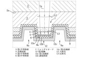
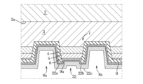
- FIG. 2 is an enlarged cross-sectional view of main parts showing the photodiode and electrodes of FIG. 1.
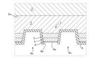
- FIG. FIG. 3 is a cross-sectional view showing a process of forming a truncated conical photodiode.
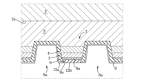
- FIG. 3 is a cross-sectional view showing a process of forming an electrode of a photodiode.
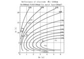
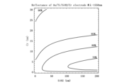
- 3 is a graph showing, in contour lines, the calculated results of the reflectance of the electrode with respect to the complex refractive index of the first metal layer of the electrode.
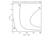
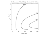
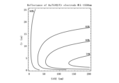
- 11 is a graph showing the relationship between the thickness of a dielectric layer, the thickness of a first metal layer, and the reflectance of an electrode when the first metal layer of the electrode is made of Ti. It is a graph showing the relationship between the thickness of the dielectric layer, the thickness of the first metal layer, and the reflectance of the electrode when the first metal layer of the electrode is Ta. It is a graph showing the relationship between the thickness of the dielectric layer, the thickness of the first metal layer, and the reflectance of the electrode when the first metal layer of the electrode is Ag. It is a graph showing the relationship between the thickness of the dielectric layer, the thickness of the first metal layer, and the reflectance of the electrode when the first metal layer of the electrode is Al.
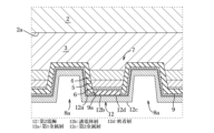
- FIG. 2 is a cross-sectional view showing an example of a photodiode including an electrode having an adhesion layer between a dielectric film and a second metal film.
- 12 is a graph showing the relationship between the thickness of the dielectric layer, the thickness of the first metal layer, and the reflectance of the electrode when the first metal layer of the electrode in FIG. 11 is made of Cr.
- FIG. 2 is a sectional view showing a conventional example of an electrode.
- 14 is a graph showing the relationship between the Ti thickness and Pt thickness of the electrode of FIG. 13 and the reflectance of this electrode.
- a back-illuminated semiconductor light-receiving device 1 includes a first semiconductor layer 3, a light absorption layer 4, and a first semiconductor layer 3, which are laminated in order from the semiconductor substrate 2 side on the front surface 2a side of a semiconductor substrate 2.
- a PIN type photodiode 7 having two semiconductor layers 5 and a third semiconductor layer 6 is provided.
- the photodiode 7 is formed into a truncated cone shape by a groove 8a formed on the outer periphery of the photodiode 7.
- the photodiode 7 is formed so that the diameter of the light absorption layer 4 is, for example, 20 ⁇ m or less, and the area is reduced to reduce the element capacitance.
- the semiconductor substrate 2 is, for example, a semi-insulating InP substrate that is transparent to the emitted light L1 having a wavelength in the infrared region (for example, 1300 to 1600 nm) emitted from the optical fiber cable OC.
- the first semiconductor layer 3 is a first conductivity type, for example, an n-InP layer.
- the light absorption layer 4 is, for example, an InGaAs layer.
- the second semiconductor layer 5 is a p-InP layer of a second conductivity type, for example.
- the third semiconductor layer 6 is, for example, an InGaAs layer formed thinner than the light absorption layer 4, and is formed for ohmic contact with an electrode (second electrode 12) to be described later.
- the groove 8a is formed by etching the first semiconductor layer 3 halfway through the third semiconductor layer 6, second semiconductor layer 5, and light absorption layer 4 by, for example, reactive ion etching. At this time, an opening 8b (hole or groove) reaching the first semiconductor layer 3 outside the photodiode 7 is also formed at the same time. Then, as shown in FIG. 3, the insulating film 9 is formed using a known method to cover a region other than most of the surface 6a of the third semiconductor layer 6 of the photodiode 7 and the bottom of the opening 8b (not shown). contact holes 9a and 9b are formed in the insulating film 9. For example, a SiO2 film, a SiN film, or the like is used as the insulating film 9.
- a first metal layer 12a connected to the third semiconductor layer 6 through the contact hole 9a is selectively formed so as to extend to the outside of the groove 8a, for example, by a known lift-off method. Ru.
- a dielectric layer 12b is selectively formed on the first metal layer 12a in a region corresponding to the photodiode 7 by a known method (film formation, photolithography, etching).
- a second metal layer 12c is selectively formed to cover the first metal layer 12a and the dielectric layer 12b by, for example, a known lift-off method, and the second electrode 12 is formed as shown in FIGS. 1 and 2. be done.
- the second metal layer 12c is connected to the first metal layer 12a on the outer peripheral side of the dielectric layer 12b.
- the first metal layer 12a and the second metal layer 12c connected to the first semiconductor layer 3 through the contact hole 9b are selectively formed so as to extend outside the opening 8b.
- the first electrode 11 is formed simultaneously with the second electrode 12.
- the first and second electrodes 11 and 12 are each connected to an external wiring section of a printed circuit board, for example.
- the second electrode 12 formed in this manner has a structure in which a first metal layer 12a, a dielectric layer 12b, and a second metal layer 12c are laminated in order from the third semiconductor layer 6 side in a portion corresponding to the photodiode 7. has.
- the first metal layer 12a has a value of the real part n (refractive index) of the complex refractive index smaller than the refractive index of the third semiconductor layer 6 and a value of the imaginary part k (extinction coefficient) of the complex refractive index of 10 or more. is made of metal.
- This first metal layer 12a is a thin film of a metal alternatively selected from the group consisting of Au (gold), Ag (silver), Al (aluminum), and Cr (chromium).
- the second metal layer 12c is often made of Au, which can be easily bonded to the outside and is difficult to oxidize.
- a condensing lens portion 2c formed integrally with the semiconductor substrate 2 and having a convex lens shape.
- the condensing lens portion 2c is formed such that the lens optical axis coincides with the central axis 7a of the photodiode 7 having a truncated cone shape.
- Output light L1 (light pulse signal) emitted from the optical fiber cable OC is emitted so that its optical axis coincides with the central axis 7a, and enters the condenser lens portion 2c while expanding conically.
- the incident light L2 that enters the condenser lens section 2c and travels through the semiconductor substrate 2 is condensed onto the photodiode 7 by the condensing action of the condenser lens section 2c.
- incident light L2 enters the photodiode 7, and a portion of it is converted into two types of charge carriers (electrons and holes) in the light absorption layer 4. Then, one charge carrier moves to the first semiconductor layer 3, and the other charge carrier moves to the second semiconductor layer 5, and is output as a photocurrent to the outside via the first and second electrodes 11 and 12. Ru. Further, the configuration is such that reflected light L3 of the incident light L2 that is not photoelectrically converted and is transmitted through the light absorption layer 4 and reflected by the second electrode 12 enters the light absorption layer 4 again. A part of the reflected light L3 re-entering the light absorption layer 4 is photoelectrically converted and outputted to the outside as a photocurrent together with charge carriers photoelectrically converted from the incident light L2 via the first and second electrodes 11 and 12. .
- the reflected light L3 re-enters the light absorption layer 4, the effective thickness of the light absorption layer 4 increases, and the sensitivity of the back-illuminated semiconductor light receiving element 1 improves. Therefore, it is possible to form the light absorption layer 4 thinly while suppressing a decrease in sensitivity, and it is possible to shorten the transit time of charge carriers and increase the response speed.
- the second electrode 12 is close to the photodiode 7, the time for light to travel back and forth between the light absorption layer 4 and the second electrode 12 is shortened, and it can be separated from the subsequent optical pulse signal. Therefore, it can support high-speed communication.
- the area of the photodiode 7 is small, the element capacitance can be reduced and the response speed can be increased.
- the incident light L2 is made incident on the small area photodiode 7 by the condenser lens section 2c, the incident light L2 can be used without waste to suppress a decrease in sensitivity.
- the reflectance of the second electrode 12 will be explained using an example in which the wavelength ⁇ of light is 1550 nm.
- a portion of the incident light L2 passes through the light absorption layer 4, passes through the second semiconductor layer 5 and the third semiconductor layer 6, and reaches the first metal layer 12a of the second electrode 12.
- the second semiconductor layer 5 is p-InP and the third semiconductor layer 6 is InGaAs
- the refractive index of the second and third semiconductor layers 5 and 6 is 3.22, respectively.
- FIG. 5 shows the reflectance of the second electrode 12 using the real part n (refractive index) and imaginary part k (extinction coefficient) of the complex refractive index of the metal of the first metal layer 12a constituting the second electrode 12 as parameters.
- the calculation results are shown in contour lines.
- the thickness of the first metal layer 12a is 20 nm
- the dielectric layer 12b is formed of a SiO2 film with a thickness of 100 nm.
- the second metal layer 12c is an Au film with a thickness of 600 nm also in the graphs from FIG. 5 onwards.
- the metals that provide a high reflectance of over 80% are Au (gold), Ag (silver), Cu (copper), and Al (aluminum). and Cr (chromium). These metals have a value of the real part n of the complex refractive index smaller than the refractive index of the third semiconductor layer 6 (InGaAs).
- Ni nickel
- Ti titanium
- Pt platinum
- Ni nickel
- Ti titanium
- Pt platinum
- Ta tantalum
- the value of the imaginary part k of the complex refractive index is smaller than that of Ag etc., so that the incident light is It is thought that the reflectance is low because it penetrates deeply from the interface.
- Cu is difficult to process compared to Au, Ag, Al, and Cr, and has the property of easily diffusing into other materials, so it is difficult to use it as the first metal layer 12a.
- FIG. 6 shows the reflectance of the second electrode 12 calculated using the thickness of the dielectric layer 12b (SiO2 film) and the thickness of the first metal layer 12a as parameters when the first metal layer 12a is made of Ti. , shown as contour lines.
- the thinner the first metal layer 12a and the thinner the dielectric layer 12b the higher the reflectance.
- the thinner the first metal layer 12a is, the more light passes through the first metal layer 12a, and the more light is reflected at the interface between the first metal layer 12a and the dielectric layer 12b and the interface between the dielectric layer 12b and the second metal layer 12c. This is thought to be due to an increase in
- FIG. 7 shows the reflectance of the second electrode 12 calculated using the thickness of the dielectric layer 12b (SiO2 film) and the thickness of the first metal layer 12a as parameters when the first metal layer 12a is formed of Ta. , shown as contour lines.
- the thickness of the dielectric layer 12b is, for example, 100 nm and the thickness of the first metal layer 12a is, for example, 20 nm
- the reflectance is less than 80%. In order to bring the reflectance close to 90%, it is necessary to make at least one of the first metal layer 12a and the dielectric layer 12b thinner, which is not easy.
- FIG. 8 shows a case where the first metal layer 12a is made of Ag.
- FIG. 9 shows a case where the first metal layer 12a is made of Al.
- FIG. 10 shows a case where the first metal layer 12a is made of Cr.
- the dielectric layer 12b has a thickness of, for example, 100 nm and the first metal layer 12a has a thickness of, for example, 20 nm
- the reflectance exceeds 85%. Therefore, when the first metal layer 12a is made of Ag, Al, or Cr, high reflectance can be easily obtained.
- the thickness of the first metal layer 12a thicker than, for example, 25 nm, it is possible to reduce the contact resistance and obtain a reflectance of 90% or more. Further, according to FIG. 3, a high reflectance can be obtained similarly when the first metal layer 12a is made of Au.
- the second electrode 12 can be formed in the same manner as shown in FIG.
- the dielectric layer 12b prevents a change in the complex refractive index due to alloying of the first metal layer 12a by preventing alloying between the first metal layer 12a and the second metal layer 12c due to mutual diffusion. Since the first metal layer 12a and the second metal layer 12c are connected on the outer peripheral side of the dielectric layer 12b, the second electrode 12 has conductivity and high reflectance. Note that, when the thickness of the first metal layer 12a is such that the contact resistance is small, the reflection by the second electrode 12 is dominated by reflection at the interface between the third semiconductor layer 6 and the first metal layer 12a, and the dielectric
- the layer 12b may be formed of, for example, a SiON film, a SiN film, etc. other than the SiO2 film.
- the second electrode 12 may include an adhesion layer 12d containing Ti as a main component at least between the dielectric layer 12b and the second metal layer 12c. Note that the thickness of the adhesive layer 12d that is generally used is about 10 nm.
- the second electrode 12 provided with the Ti adhesion layer 12d can obtain a high reflectance.
- the reflectance exceeds 85%, which is the same level of reflection as the second electrode 12 in FIG. 10 without the adhesive layer 12d. rate is obtained.
- the adhesion layer 12d can prevent the second metal layer 12c from peeling off or lifting, thereby preventing the function of the second electrode 12A from being impaired.
- FIG. 13 shows a photodiode 7 in which the second electrode 12 is replaced with a conventional electrode 22 having a conventional structure.
- the conventional electrode 22 is formed by laminating, in order from the third semiconductor layer 6 side, a Ti layer 22a, a Pt layer 22b as a barrier layer for preventing alloying during bonding with the outside, and an Au layer 22c.
- the value of the real part n of the complex refractive index of the Ti layer 22a is larger than the refractive index of the third semiconductor layer 6, and the value of the real part n of the complex refractive index of the Pt layer 22b is larger than the value of the complex refractive index of the Ti layer 22a.
- the second electrode 12 is formed of a metal in which the value of the real part n of the complex refractive index is smaller than the refractive index of the third semiconductor layer 6, and the value of the imaginary part k of the complex refractive index is 10 or more. It has a first metal layer 12a. With this structure including the dielectric layer 12b between the first metal layer 12a and the second metal layer 12c, higher reflectance than before can be obtained. Therefore, most of the light transmitted through the light absorption layer 4 can be reflected by the second electrode 12 close to the photodiode 7 and can be made to enter the light absorption layer 4 again. Therefore, the light absorption layer 4 can be made thinner while suppressing a decrease in sensitivity of the back-illuminated semiconductor light-receiving element 1, and the response speed can be increased.
- the first metal layer 12a is made of a metal such as Au, Ag, or Cr, in which the value of the real part n of the complex refractive index is smaller than the refractive index of the third semiconductor layer 6 and the value of the imaginary part k of the complex refractive index is 10 or more. and Al. Since these metals are commonly used as materials for semiconductor devices, the second electrode 12 with high reflectance can be easily formed.
- the second electrode 12 may have an adhesion layer 12d containing Ti as a main component between the dielectric layer 12b and the second metal layer 12c.
- the adhesion layer 12d can prevent film lifting or peeling of the second metal layer 12c, which is a concern when the adhesion between the second metal layer 12c and the dielectric layer 12b is not good. Therefore, deterioration in the function of the second electrode 12 due to film lifting or film peeling can be prevented.
- the photodiode 7 is formed in the shape of a truncated cone such that the diameter of the light absorption layer 4 is 20 ⁇ m or less, and the optical axis of the lens is aligned with the central axis 7a of the truncated cone-shaped photodiode 7 on the back surface 2b of the semiconductor substrate 2. It has a condensing lens section 2c. Since the area of the photodiode 7 is small, the element capacitance can be reduced, and the response speed can be increased.
- the condenser lens section 2c By condensing the light and making it incident on the photodiode 7, which has a small area, using the condenser lens section 2c, it is possible to suppress a decrease in the sensitivity of the back-illuminated semiconductor light-receiving element 1. Note that the diameter of the light absorption layer 4 can be appropriately set depending on the required response frequency band.
Landscapes
- Light Receiving Elements (AREA)
Priority Applications (2)
| Application Number | Priority Date | Filing Date | Title |
|---|---|---|---|
| JP2024546586A JP7755755B2 (ja) | 2022-09-14 | 2022-09-14 | 裏面入射型半導体受光素子 |
| PCT/JP2022/034374 WO2024057435A1 (ja) | 2022-09-14 | 2022-09-14 | 裏面入射型半導体受光素子 |
Applications Claiming Priority (1)
| Application Number | Priority Date | Filing Date | Title |
|---|---|---|---|
| PCT/JP2022/034374 WO2024057435A1 (ja) | 2022-09-14 | 2022-09-14 | 裏面入射型半導体受光素子 |
Publications (1)
| Publication Number | Publication Date |
|---|---|
| WO2024057435A1 true WO2024057435A1 (ja) | 2024-03-21 |
Family
ID=90274596
Family Applications (1)
| Application Number | Title | Priority Date | Filing Date |
|---|---|---|---|
| PCT/JP2022/034374 Ceased WO2024057435A1 (ja) | 2022-09-14 | 2022-09-14 | 裏面入射型半導体受光素子 |
Country Status (2)
| Country | Link |
|---|---|
| JP (1) | JP7755755B2 (cg-RX-API-DMAC7.html) |
| WO (1) | WO2024057435A1 (cg-RX-API-DMAC7.html) |
Citations (6)
| Publication number | Priority date | Publication date | Assignee | Title |
|---|---|---|---|---|
| JP2002252366A (ja) * | 2000-12-19 | 2002-09-06 | Fujitsu Quantum Devices Ltd | 半導体受光装置 |
| JP2006120913A (ja) * | 2004-10-22 | 2006-05-11 | Toyoda Gosei Co Ltd | 半導体発光素子 |
| JP2013131637A (ja) * | 2011-12-21 | 2013-07-04 | Japan Oclaro Inc | 光モジュール |
| JP2014007285A (ja) * | 2012-06-25 | 2014-01-16 | Nippon Telegr & Teleph Corp <Ntt> | フォトダイオード |
| CN112768550A (zh) * | 2020-12-18 | 2021-05-07 | 中国电子科技集团公司第四十四研究所 | 一种用于提高背照式光电二极管响应度的结构及制作方法 |
| WO2022149253A1 (ja) * | 2021-01-08 | 2022-07-14 | 株式会社京都セミコンダクター | 半導体受光素子 |
Family Cites Families (2)
| Publication number | Priority date | Publication date | Assignee | Title |
|---|---|---|---|---|
| JP2011100892A (ja) | 2009-11-06 | 2011-05-19 | Sumitomo Electric Ind Ltd | 電子機器、複合型電子機器、検出装置、受光素子アレイ、および、これらの製造方法 |
| JP2011124450A (ja) | 2009-12-11 | 2011-06-23 | Nec Corp | 半導体受光素子 |
-
2022
- 2022-09-14 JP JP2024546586A patent/JP7755755B2/ja active Active
- 2022-09-14 WO PCT/JP2022/034374 patent/WO2024057435A1/ja not_active Ceased
Patent Citations (6)
| Publication number | Priority date | Publication date | Assignee | Title |
|---|---|---|---|---|
| JP2002252366A (ja) * | 2000-12-19 | 2002-09-06 | Fujitsu Quantum Devices Ltd | 半導体受光装置 |
| JP2006120913A (ja) * | 2004-10-22 | 2006-05-11 | Toyoda Gosei Co Ltd | 半導体発光素子 |
| JP2013131637A (ja) * | 2011-12-21 | 2013-07-04 | Japan Oclaro Inc | 光モジュール |
| JP2014007285A (ja) * | 2012-06-25 | 2014-01-16 | Nippon Telegr & Teleph Corp <Ntt> | フォトダイオード |
| CN112768550A (zh) * | 2020-12-18 | 2021-05-07 | 中国电子科技集团公司第四十四研究所 | 一种用于提高背照式光电二极管响应度的结构及制作方法 |
| WO2022149253A1 (ja) * | 2021-01-08 | 2022-07-14 | 株式会社京都セミコンダクター | 半導体受光素子 |
Also Published As
| Publication number | Publication date |
|---|---|
| JP7755755B2 (ja) | 2025-10-16 |
| JPWO2024057435A1 (cg-RX-API-DMAC7.html) | 2024-03-21 |
Similar Documents
| Publication | Publication Date | Title |
|---|---|---|
| CA2365454C (en) | Semiconductor photodetection device | |
| JP4157698B2 (ja) | 半導体受光素子およびその駆動方法 | |
| JP3601761B2 (ja) | 受光素子およびその製造方法 | |
| US20020110950A1 (en) | Method of fabricating a light receiving device | |
| JP4291521B2 (ja) | 半導体受光素子、半導体受光装置、半導体装置、光モジュール及び光伝送装置 | |
| JP7755755B2 (ja) | 裏面入射型半導体受光素子 | |
| JP2014013844A (ja) | 半導体受光素子およびその製造方法 | |
| EP4510196A1 (en) | Light-receiving element | |
| JP3674255B2 (ja) | 受光素子の製造方法 | |
| CN114284390B (zh) | 垂直入射超宽带集成型光电探测器芯片及其制作方法 | |
| JP2952906B2 (ja) | フォトダイオード | |
| US6184054B1 (en) | Optical electronic IC capable of photo detection and its process | |
| EP3792983B1 (en) | Light-receiving element unit | |
| JP4048217B2 (ja) | 半導体受光装置 | |
| JPH05267708A (ja) | 光半導体装置の電極構造 | |
| US20240044701A1 (en) | Light sensor structure and manufacturing method thereof | |
| TWI900633B (zh) | 光檢測裝置 | |
| JP2968440B2 (ja) | 半導体受光素子 | |
| JPH05102513A (ja) | 半導体受光素子 | |
| Makiuchi et al. | Flip-chip planar GaInAs/InP pin photodiodes-fabrication and characteristics | |
| KR20010009571A (ko) | 광검출기 디바이스 및 그 제조방법 | |
| JP2562569Y2 (ja) | フオトダイオード | |
| JP4058457B2 (ja) | 半導体受光装置 | |
| JPH10163516A (ja) | 半導体受光素子 | |
| JPH03296279A (ja) | 半導体受光素子 |
Legal Events
| Date | Code | Title | Description |
|---|---|---|---|
| 121 | Ep: the epo has been informed by wipo that ep was designated in this application |
Ref document number: 22958763 Country of ref document: EP Kind code of ref document: A1 |
|
| WWE | Wipo information: entry into national phase |
Ref document number: 2024546586 Country of ref document: JP |
|
| NENP | Non-entry into the national phase |
Ref country code: DE |
|
| 122 | Ep: pct application non-entry in european phase |
Ref document number: 22958763 Country of ref document: EP Kind code of ref document: A1 |