WO2024053457A1 - 半導体装置 - Google Patents
半導体装置 Download PDFInfo
- Publication number
- WO2024053457A1 WO2024053457A1 PCT/JP2023/030991 JP2023030991W WO2024053457A1 WO 2024053457 A1 WO2024053457 A1 WO 2024053457A1 JP 2023030991 W JP2023030991 W JP 2023030991W WO 2024053457 A1 WO2024053457 A1 WO 2024053457A1
- Authority
- WO
- WIPO (PCT)
- Prior art keywords
- region
- contact
- trench
- gate
- semiconductor device
- Prior art date
- Legal status (The legal status is an assumption and is not a legal conclusion. Google has not performed a legal analysis and makes no representation as to the accuracy of the status listed.)
- Ceased
Links
Images


Classifications
-
- H—ELECTRICITY
- H10—SEMICONDUCTOR DEVICES; ELECTRIC SOLID-STATE DEVICES NOT OTHERWISE PROVIDED FOR
- H10D—INORGANIC ELECTRIC SEMICONDUCTOR DEVICES
- H10D64/00—Electrodes of devices having potential barriers
- H10D64/111—Field plates
- H10D64/117—Recessed field plates, e.g. trench field plates or buried field plates
-
- H—ELECTRICITY
- H10—SEMICONDUCTOR DEVICES; ELECTRIC SOLID-STATE DEVICES NOT OTHERWISE PROVIDED FOR
- H10D—INORGANIC ELECTRIC SEMICONDUCTOR DEVICES
- H10D12/00—Bipolar devices controlled by the field effect, e.g. insulated-gate bipolar transistors [IGBT]
-
- H—ELECTRICITY
- H10—SEMICONDUCTOR DEVICES; ELECTRIC SOLID-STATE DEVICES NOT OTHERWISE PROVIDED FOR
- H10D—INORGANIC ELECTRIC SEMICONDUCTOR DEVICES
- H10D12/00—Bipolar devices controlled by the field effect, e.g. insulated-gate bipolar transistors [IGBT]
- H10D12/411—Insulated-gate bipolar transistors [IGBT]
- H10D12/441—Vertical IGBTs
- H10D12/461—Vertical IGBTs having non-planar surfaces, e.g. having trenches, recesses or pillars in the surfaces of the emitter, base or collector regions
- H10D12/481—Vertical IGBTs having non-planar surfaces, e.g. having trenches, recesses or pillars in the surfaces of the emitter, base or collector regions having gate structures on slanted surfaces, on vertical surfaces, or in grooves, e.g. trench gate IGBTs
-
- H—ELECTRICITY
- H10—SEMICONDUCTOR DEVICES; ELECTRIC SOLID-STATE DEVICES NOT OTHERWISE PROVIDED FOR
- H10D—INORGANIC ELECTRIC SEMICONDUCTOR DEVICES
- H10D30/00—Field-effect transistors [FET]
- H10D30/01—Manufacture or treatment
- H10D30/021—Manufacture or treatment of FETs having insulated gates [IGFET]
-
- H—ELECTRICITY
- H10—SEMICONDUCTOR DEVICES; ELECTRIC SOLID-STATE DEVICES NOT OTHERWISE PROVIDED FOR
- H10D—INORGANIC ELECTRIC SEMICONDUCTOR DEVICES
- H10D30/00—Field-effect transistors [FET]
- H10D30/60—Insulated-gate field-effect transistors [IGFET]
-
- H—ELECTRICITY
- H10—SEMICONDUCTOR DEVICES; ELECTRIC SOLID-STATE DEVICES NOT OTHERWISE PROVIDED FOR
- H10D—INORGANIC ELECTRIC SEMICONDUCTOR DEVICES
- H10D62/00—Semiconductor bodies, or regions thereof, of devices having potential barriers
- H10D62/10—Shapes, relative sizes or dispositions of the regions of the semiconductor bodies; Shapes of the semiconductor bodies
- H10D62/124—Shapes, relative sizes or dispositions of the regions of semiconductor bodies or of junctions between the regions
- H10D62/126—Top-view geometrical layouts of the regions or the junctions
- H10D62/127—Top-view geometrical layouts of the regions or the junctions of cellular field-effect devices, e.g. multicellular DMOS transistors or IGBTs
-
- H—ELECTRICITY
- H10—SEMICONDUCTOR DEVICES; ELECTRIC SOLID-STATE DEVICES NOT OTHERWISE PROVIDED FOR
- H10D—INORGANIC ELECTRIC SEMICONDUCTOR DEVICES
- H10D62/00—Semiconductor bodies, or regions thereof, of devices having potential barriers
- H10D62/10—Shapes, relative sizes or dispositions of the regions of the semiconductor bodies; Shapes of the semiconductor bodies
- H10D62/13—Semiconductor regions connected to electrodes carrying current to be rectified, amplified or switched, e.g. source or drain regions
- H10D62/141—Anode or cathode regions of thyristors; Collector or emitter regions of gated bipolar-mode devices, e.g. of IGBTs
- H10D62/145—Emitter regions of IGBTs
-
- H—ELECTRICITY
- H10—SEMICONDUCTOR DEVICES; ELECTRIC SOLID-STATE DEVICES NOT OTHERWISE PROVIDED FOR
- H10D—INORGANIC ELECTRIC SEMICONDUCTOR DEVICES
- H10D62/00—Semiconductor bodies, or regions thereof, of devices having potential barriers
- H10D62/10—Shapes, relative sizes or dispositions of the regions of the semiconductor bodies; Shapes of the semiconductor bodies
- H10D62/17—Semiconductor regions connected to electrodes not carrying current to be rectified, amplified or switched, e.g. channel regions
- H10D62/393—Body regions of DMOS transistors or IGBTs
-
- H—ELECTRICITY
- H10—SEMICONDUCTOR DEVICES; ELECTRIC SOLID-STATE DEVICES NOT OTHERWISE PROVIDED FOR
- H10D—INORGANIC ELECTRIC SEMICONDUCTOR DEVICES
- H10D64/00—Electrodes of devices having potential barriers
- H10D64/20—Electrodes characterised by their shapes, relative sizes or dispositions
-
- H—ELECTRICITY
- H10—SEMICONDUCTOR DEVICES; ELECTRIC SOLID-STATE DEVICES NOT OTHERWISE PROVIDED FOR
- H10D—INORGANIC ELECTRIC SEMICONDUCTOR DEVICES
- H10D64/00—Electrodes of devices having potential barriers
- H10D64/20—Electrodes characterised by their shapes, relative sizes or dispositions
- H10D64/23—Electrodes carrying the current to be rectified, amplified, oscillated or switched, e.g. sources, drains, anodes or cathodes
- H10D64/232—Emitter electrodes for IGBTs
-
- H—ELECTRICITY
- H10—SEMICONDUCTOR DEVICES; ELECTRIC SOLID-STATE DEVICES NOT OTHERWISE PROVIDED FOR
- H10D—INORGANIC ELECTRIC SEMICONDUCTOR DEVICES
- H10D64/00—Electrodes of devices having potential barriers
- H10D64/20—Electrodes characterised by their shapes, relative sizes or dispositions
- H10D64/23—Electrodes carrying the current to be rectified, amplified, oscillated or switched, e.g. sources, drains, anodes or cathodes
- H10D64/251—Source or drain electrodes for field-effect devices
- H10D64/256—Source or drain electrodes for field-effect devices for lateral devices wherein the source or drain electrodes are recessed in semiconductor bodies
-
- H—ELECTRICITY
- H10—SEMICONDUCTOR DEVICES; ELECTRIC SOLID-STATE DEVICES NOT OTHERWISE PROVIDED FOR
- H10D—INORGANIC ELECTRIC SEMICONDUCTOR DEVICES
- H10D64/00—Electrodes of devices having potential barriers
- H10D64/20—Electrodes characterised by their shapes, relative sizes or dispositions
- H10D64/27—Electrodes not carrying the current to be rectified, amplified, oscillated or switched, e.g. gates
- H10D64/311—Gate electrodes for field-effect devices
- H10D64/411—Gate electrodes for field-effect devices for FETs
- H10D64/511—Gate electrodes for field-effect devices for FETs for IGFETs
- H10D64/512—Disposition of the gate electrodes, e.g. buried gates
- H10D64/513—Disposition of the gate electrodes, e.g. buried gates within recesses in the substrate, e.g. trench gates, groove gates or buried gates
-
- H—ELECTRICITY
- H10—SEMICONDUCTOR DEVICES; ELECTRIC SOLID-STATE DEVICES NOT OTHERWISE PROVIDED FOR
- H10D—INORGANIC ELECTRIC SEMICONDUCTOR DEVICES
- H10D64/00—Electrodes of devices having potential barriers
- H10D64/20—Electrodes characterised by their shapes, relative sizes or dispositions
- H10D64/27—Electrodes not carrying the current to be rectified, amplified, oscillated or switched, e.g. gates
- H10D64/311—Gate electrodes for field-effect devices
- H10D64/411—Gate electrodes for field-effect devices for FETs
- H10D64/511—Gate electrodes for field-effect devices for FETs for IGFETs
- H10D64/517—Gate electrodes for field-effect devices for FETs for IGFETs characterised by the conducting layers
- H10D64/519—Gate electrodes for field-effect devices for FETs for IGFETs characterised by the conducting layers characterised by their top-view geometrical layouts
-
- H—ELECTRICITY
- H10—SEMICONDUCTOR DEVICES; ELECTRIC SOLID-STATE DEVICES NOT OTHERWISE PROVIDED FOR
- H10D—INORGANIC ELECTRIC SEMICONDUCTOR DEVICES
- H10D64/00—Electrodes of devices having potential barriers
- H10D64/60—Electrodes characterised by their materials
- H10D64/66—Electrodes having a conductor capacitively coupled to a semiconductor by an insulator, e.g. MIS electrodes
-
- H—ELECTRICITY
- H10—SEMICONDUCTOR DEVICES; ELECTRIC SOLID-STATE DEVICES NOT OTHERWISE PROVIDED FOR
- H10D—INORGANIC ELECTRIC SEMICONDUCTOR DEVICES
- H10D12/00—Bipolar devices controlled by the field effect, e.g. insulated-gate bipolar transistors [IGBT]
- H10D12/01—Manufacture or treatment
- H10D12/031—Manufacture or treatment of IGBTs
- H10D12/032—Manufacture or treatment of IGBTs of vertical IGBTs
- H10D12/035—Etching a recess in the emitter region
-
- H—ELECTRICITY
- H10—SEMICONDUCTOR DEVICES; ELECTRIC SOLID-STATE DEVICES NOT OTHERWISE PROVIDED FOR
- H10D—INORGANIC ELECTRIC SEMICONDUCTOR DEVICES
- H10D12/00—Bipolar devices controlled by the field effect, e.g. insulated-gate bipolar transistors [IGBT]
- H10D12/01—Manufacture or treatment
- H10D12/031—Manufacture or treatment of IGBTs
- H10D12/032—Manufacture or treatment of IGBTs of vertical IGBTs
- H10D12/038—Manufacture or treatment of IGBTs of vertical IGBTs having a recessed gate, e.g. trench-gate IGBTs
Definitions
- the present disclosure relates to a semiconductor device.
- Patent Document 1 discloses a semiconductor layer having a main surface in which a trench is formed, a body region of a first conductivity type formed along a sidewall of the trench in a surface portion of the main surface of the semiconductor layer, and a body region of the body. a second conductivity type impurity region formed along the sidewalls of the trench in the surface portion of the region; a gate insulating layer formed on the inner wall of the trench; and an impurity region buried in the trench and sandwiching the gate insulating layer.
- a semiconductor device is disclosed, including a contact electrode connected to the trench, and a buried insulating layer interposed between the gate electrode and the contact electrode in the trench and insulating the gate electrode and the contact electrode.
- An embodiment of the present disclosure provides a semiconductor device that can improve the degree of freedom in designing dimensions of first impurity regions such as an emitter region and a source region, thereby improving breakdown resistance.
- An embodiment of the present disclosure provides a semiconductor device that can suppress reduction in channel width and reduce on-resistance in a structure including a contact trench that intersects with a gate trench.
- a semiconductor device includes a chip having a first main surface in which a gate trench extending in a first direction having a bottom wall and a side wall is formed, and the gate trench is formed in a surface portion of the first main surface.
- a body region of a first conductivity type formed along the sidewall of the gate trench;
- a first impurity region of a second conductivity type formed along the sidewall of the gate trench in a surface portion of the body region;
- a gate insulating layer formed on the bottom wall and the side wall of the trench, a gate electrode embedded in the gate trench and facing the body region and the first impurity region with the gate insulating layer in between, and the gate trench.
- a contact trench that includes an intersection region that intersects with the first direction, and is drawn out from the intersection region to the outside of the gate trench along a second direction that intersects with the first direction; a contact electrode electrically connected to the body region and the first impurity region, and a space region is formed on the gate electrode in at least the crossing region and a peripheral portion of the crossing region in the gate trench.
- a covering insulating layer is embedded in the spatial region to cover the upper surface of the gate electrode in the intersection region and a peripheral portion of the intersection region, and to insulate between the gate electrode and the contact electrode.
- the first impurity region is formed deeper than the upper surface of the gate electrode in a peripheral portion of the intersection region.
- the first impurity region is formed deeper than the upper surface of the gate electrode in the peripheral portion of the intersection region. Therefore, a channel can be formed in the periphery of the intersection region, so that reduction in channel width can be suppressed and on-resistance can be reduced.
- the first impurity region is formed deeper than the upper surface of the gate electrode. This allows a channel to be formed also in the lower region around the intersection region. Therefore, there is no need to consider the patterning margin during etching or contact pattern formation, and the degree of freedom in designing the dimensions of the first impurity region can be improved, thereby improving the breakdown resistance.
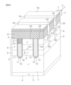
- FIG. 1 is a schematic cross-sectional perspective view showing a partial region of a semiconductor device according to a first embodiment of the present disclosure.
- FIG. 2 is a diagram in which the structure on the first main surface of the chip is removed from FIG. 1.
- FIG. 3 is a diagram from FIG. 2 with the emitter contact electrode layer removed.
- FIG. 4 is a schematic plan view of FIG. 3 viewed from the first main surface of the chip.
- FIG. 5 is a sectional view taken along the line VV shown in FIG. 4.
- FIG. 6 is a cross-sectional view taken along line VI-VI shown in FIG. 4.
- FIG. 7 is a cross-sectional view taken along line VII-VII shown in FIG. 4.
- FIG. 8A is a diagram illustrating an example of a method for manufacturing the semiconductor device.
- FIG. 8A is a diagram illustrating an example of a method for manufacturing the semiconductor device.
- FIG. 8B is a diagram showing a step after FIG. 8A.
- FIG. 8C is a diagram showing a step after FIG. 8B.
- FIG. 8D is a diagram showing a step after FIG. 8C.
- FIG. 8E is a diagram showing a step after FIG. 8D.
- FIG. 8F is a diagram showing a step after FIG. 8E.
- FIG. 8G is a diagram showing a step after FIG. 8F.
- FIG. 8H is a diagram showing a step after FIG. 8G.
- FIG. 8I is a diagram showing a step after FIG. 8H.
- FIG. 8J is a diagram showing a step after FIG. 8I.
- FIG. 8K is a diagram showing a step after FIG. 8J.
- FIG. 8L is a diagram showing a step after FIG. 8K.
- FIG. 8M is a diagram showing a step after FIG. 8L.
- FIG. 8N is a diagram showing a step after FIG. 8M.
- FIG. 9A is a diagram for explaining channel formation in a semiconductor device according to condition 1.
- FIG. 9B is a diagram for explaining the arrangement pattern of the emitter region and contact region of the semiconductor device according to Condition 1.
- FIG. 10A is a diagram for explaining channel formation in a semiconductor device according to Condition 2.
- FIG. 10B is a diagram for explaining the arrangement pattern of the emitter region and contact region of the semiconductor device according to Condition 2.
- FIG. 11 is a graph obtained by simulation of short-circuit waveforms of the semiconductor device according to Conditions 1 and 2.
- FIG. 12 is a graph obtained by simulation of the current-voltage characteristics of the semiconductor device according to Conditions 1 and 2.
- FIG. 13 is an enlarged view of a part of the graph of FIG. 12.
- FIG. 14 is a graph obtained by simulation of the current-voltage characteristics of the semiconductor device according to Conditions 1 and 2.
- FIG. 15 is a schematic cross-sectional perspective view showing a partial region of a semiconductor device according to a second embodiment of the present disclosure.
- FIG. 16 is a schematic cross-sectional view showing a part of the semiconductor device of FIG. 15.
- FIG. 17 is a schematic cross-sectional view showing a part of the semiconductor device of FIG. 15.
- FIG. 18 is a schematic cross-sectional perspective view showing a partial region of a semiconductor device according to a third embodiment of the present disclosure.
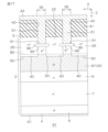
- FIG. 1 is a schematic cross-sectional perspective view showing a partial region of a semiconductor device 1 according to a first embodiment of the present disclosure.
- FIG. 2 is a diagram in which the structure on the first main surface 3 of the chip 2 is removed from FIG. 1.
- FIG. 3 is a diagram from FIG. 2 with the emitter contact electrode layer 51 removed.
- FIG. 4 is a schematic plan view of FIG. 3 viewed from the first main surface 3 of the chip 2.
- FIG. 5 is a sectional view taken along the line VV shown in FIG. 4.
- FIG. 6 is a cross-sectional view taken along line VI-VI shown in FIG. 4.
- FIG. 7 is a cross-sectional view taken along line VII-VII shown in FIG. 4. 5 to 7 also illustrate the structure on the first main surface 3 of the chip 2.
- the semiconductor device 1 has a basic configuration including a trench gate type IGBT (Insulated Gate Bipolar Transistor).
- semiconductor device 1 includes an n ⁇ type chip 2.
- the chip 2 is made of an n - type silicon single crystal substrate.
- the silicon single crystal substrate is formed using an n ⁇ type silicon single crystal semiconductor wafer manufactured through the FZ (Floating Zone) method.
- the chip 2 may be called a semiconductor chip or a semiconductor layer.
- the chip 2 has a first main surface 3 on one side and a second main surface 4 on the other side.
- the thickness of the chip 2 may be 50 ⁇ m or more and 300 ⁇ m or less.
- the thickness of the chip 2 may be 50 ⁇ m or more and 100 ⁇ m or less, 100 ⁇ m or more and 150 ⁇ m or less, 150 ⁇ m or more and 200 ⁇ m or less, 200 ⁇ m or more and 250 ⁇ m or less, or 250 ⁇ m or more and 300 ⁇ m or less.
- a p-type collector region 5 is formed on the surface portion of the second main surface 4.
- An n-type charge storage region 6 is formed in the surface portion of the first main surface 3 .
- the charge storage region 6 is formed at a distance from the collector region 5 on the first main surface 3 side.
- an n ⁇ type drift region 7 is formed in a region between the collector region 5 and the charge storage region 6.
- Drift region 7 is formed by a region located between collector region 5 and charge storage region 6 in chip 2 .
- a p-type body region 8 is formed on the surface of the charge storage region 6 .
- a plurality of trench gate electrode structures 10 and a plurality of trench emitter electrode structures 11 are formed at intervals on the surface portion of the first main surface 3.
- FIGS. 1 to 7 only one trench gate electrode structure 10 and one trench emitter electrode structure 11 adjacent to each other are shown.
- the structure of the semiconductor device 1 will be described below, focusing on the structure of one trench gate electrode structure 10 and one trench emitter electrode structure 11.
- the trench gate electrode structure 10 and the trench emitter electrode structure 11 extend in a band shape along an arbitrary first direction X in plan view.
- the trench gate electrode structure 10 and the trench emitter electrode structure 11 are formed at intervals along a second direction Y that intersects the first direction X.
- planar view refers to a planar view seen from the normal direction Z of the first principal surface 3 (hereinafter simply referred to as "normal direction Z"). More specifically, the second direction Y is a direction perpendicular to the first direction X. The first direction X and the second direction Y are also tangential directions of the first main surface 3.
- the trench pitch P0 between the trench gate electrode structure 10 and the trench emitter electrode structure 11 may be 0.1 ⁇ m or more and less than 0.6 ⁇ m.
- Trench pitch P0 is 0.1 ⁇ m or more and 0.2 ⁇ m or less, 0.2 ⁇ m or more and 0.3 ⁇ m or less, 0.3 ⁇ m or more and 0.4 ⁇ m or less, 0.4 ⁇ m or more and 0.5 ⁇ m or less, or 0.5 ⁇ m or more and 0.6 ⁇ m It may be less than
- the trench pitch P0 is preferably 0.2 ⁇ m or more and 0.4 ⁇ m or less (for example, about 0.25 ⁇ m).
- the trench gate electrode structure 10 includes a gate trench 12 , a gate insulating layer 13 , a gate electrode layer 14 , a plurality of gate electrode recesses 15 (space regions), and a plurality of gate covering insulating layers 16 .
- Gate trench 12 extends from first main surface 3 through body region 8 and charge storage region 6 to drift region 7 .
- the depth of the gate trench 12 may be 2.0 ⁇ m or more and 4.0 ⁇ m or less.
- the depth of the gate trench 12 may be 2.0 ⁇ m or more and 2.5 ⁇ m or less, 2.5 ⁇ m or more and 3.0 ⁇ m or less, 3.0 ⁇ m or more and 3.5 ⁇ m or less, or 3.5 ⁇ m or more and 4.0 ⁇ m or less.
- the depth of the gate trench 12 is preferably 2.5 ⁇ m or more and 3.5 ⁇ m or less (for example, about 3.0 ⁇ m).
- the width of the gate trench 12 in the second direction may be 0.5 ⁇ m or more and 1.5 ⁇ m or less.
- the width of the gate trench 12 in the second direction is 0.5 ⁇ m or more and 0.75 ⁇ m or less, 0.75 ⁇ m or more and 1.0 ⁇ m or less, 1.0 ⁇ m or more and 1.25 ⁇ m or less, or 1.25 ⁇ m or more and 1.5 ⁇ m or less. Good too.
- the width of the gate trench 12 in the second direction is preferably 0.5 ⁇ m or more and 1.0 ⁇ m or less (for example, about 0.75 ⁇ m).
- the gate insulating layer 13 may be formed of silicon oxide.
- the gate insulating layer 13 is formed in a film shape along the inner wall of the gate trench 12 .
- Gate insulating layer 13 defines a concave space within gate trench 12 .
- the gate electrode layer 14 may be formed of conductive polysilicon. Gate electrode layer 14 is controlled by gate voltage. The gate electrode layer 14 is embedded in the gate trench 12 with the gate insulating layer 13 in between. More specifically, the gate electrode layer 14 is embedded in a concave space defined by the gate insulating layer 13 within the gate trench 12 . The upper end of the gate electrode layer 14 is located on the first main surface 3 side with respect to the bottom of the body region 8 .
- the plurality of gate electrode recesses 15 are formed on the main surface of the gate electrode layer 14 at intervals along the first direction X.
- the upper end portion of the gate electrode layer 14 has an uneven structure including a plurality of gate electrode recesses 15.
- the interval between the plurality of gate electrode recesses 15 adjacent to each other may be greater than 0 ⁇ m and less than or equal to 10 ⁇ m.
- the interval between the plurality of gate electrode recesses 15 adjacent to each other is also the width in the first direction X of a portion of the gate electrode layer 14 sandwiched between two gate electrode recesses 15 adjacent to each other.
- the interval between the plurality of gate electrode recesses 15 adjacent to each other may be more than 0 ⁇ m and less than 2 ⁇ m, more than 2 ⁇ m and less than 4 ⁇ m, more than 4 ⁇ m and less than 6 ⁇ m, more than 6 ⁇ m and less than 8 ⁇ m, or more than 8 ⁇ m and less than 10 ⁇ m.
- each gate electrode recess 15 are formed by the gate insulating layer 13 and the gate electrode layer 14.
- the bottom wall 22 of each gate electrode recess 15 is formed of the gate electrode layer 14. Referring to FIGS. 6 and 7, the bottom wall 22 of each gate electrode recess 15 is located in a region between the first main surface 3 and the bottom 50 of the emitter region 25 (described later) with respect to the normal direction Z. There is.
- each gate electrode recess 15 is formed in a tapered shape with a bottom area smaller than the opening area.
- the angle ⁇ formed by the main surface of the gate electrode layer 14 and the side wall of the gate electrode recess 15 within the gate electrode layer 14 may be more than 90° and less than or equal to 105° (for example, about 102°).
- the plurality of gate covering insulating layers 16 are each embedded in the upper end portion of the gate electrode layer 14 within the gate trench 12. More specifically, the gate covering insulating layer 16 is embedded independently in each gate electrode recess 15. Each gate covering insulating layer 16 is exposed through the opening of the gate trench 12.
- the trench emitter electrode structure 11 includes an emitter trench 17, an emitter insulating layer 18, an emitter electrode layer 19, an emitter electrode recess 20, and an emitter covering insulating layer 21.
- Emitter trench 17 extends from first main surface 3 through body region 8 and charge storage region 6 to drift region 7 .
- the depth of the emitter trench 17 may be 2.0 ⁇ m or more and 4.0 ⁇ m or less.
- the depth of the emitter trench 17 may be 2.0 ⁇ m or more and 2.5 ⁇ m or less, 2.5 ⁇ m or more and 3.0 ⁇ m or less, 3.0 ⁇ m or more and 3.5 ⁇ m or less, or 3.5 ⁇ m or more and 4.0 ⁇ m or less.
- the depth of the emitter trench 17 is preferably 2.5 ⁇ m or more and 3.5 ⁇ m or less (for example, about 3.0 ⁇ m).
- the depth of emitter trench 17 is approximately equal to the depth of gate trench 12.
- the width of the emitter trench 17 in the second direction may be 0.5 ⁇ m or more and 1.5 ⁇ m or less.
- the width in the second direction of the emitter trench 17 is 0.5 ⁇ m or more and 0.75 ⁇ m or less, 0.75 ⁇ m or more and 1.0 ⁇ m or less, 1.0 ⁇ m or more and 1.25 ⁇ m or less, or 1.25 ⁇ m or more and 1.5 ⁇ m or less.
- the width of the emitter trench 17 in the second direction is preferably 0.5 ⁇ m or more and 1.0 ⁇ m or less (for example, about 0.75 ⁇ m).
- the width of the emitter trench 17 in the second direction is preferably approximately equal to the width of the gate trench 12 in the second direction.
- the emitter insulating layer 18 may be formed of silicon oxide. Emitter insulating layer 18 is formed in a film shape along the inner wall surface of emitter trench 17 . Emitter insulating layer 18 defines a concave space within emitter trench 17 .
- the emitter electrode layer 19 may be formed of conductive polysilicon. Emitter electrode layer 19 is controlled by emitter voltage. The emitter voltage has a voltage value less than the gate voltage. The emitter voltage may be a reference voltage (eg, ground voltage). Emitter electrode layer 19 is embedded in emitter trench 17 with emitter insulating layer 18 in between. More specifically, the emitter electrode layer 19 is embedded in a concave space defined by the emitter insulating layer 18 in the emitter trench 17 .
- the emitter electrode recess 20 is formed so as to dig down almost the entire main surface of the emitter electrode layer 19. In other words, the emitter electrode layer 19 is buried halfway in the depth direction of the concave space defined by the emitter insulating layer 18 .
- the side walls of the emitter electrode recess 20 are formed by the emitter insulating layer 18 in this embodiment.
- the bottom wall of the emitter electrode recess 20 is formed by the emitter electrode layer 19.
- the bottom wall of the emitter electrode recess 20 is located in a region between the first main surface 3 and the bottom 50 of the emitter region 25 (described later) with respect to the normal direction Z. That is, the upper end of the emitter electrode layer 19 is located on the first main surface 3 side with respect to the bottom 50 of the emitter region 25.
- the depth of the emitter electrode recess 20 may be approximately equal to the depth of the gate electrode recess 15.
- the emitter covering insulating layer 21 is embedded in the upper surface of the emitter electrode layer 19 within the emitter trench 17. More specifically, the emitter covering insulating layer 21 is embedded in the emitter electrode recess 20. Thereby, the emitter covering insulating layer 21 seals the emitter electrode layer 19. Emitter covering insulating layer 21 is exposed through the opening of emitter trench 17 .
- n + type emitter region 25 (first impurity region) is formed in a region along the sidewall of the gate trench 12 in the surface portion of the body region 8 . More specifically, a plurality of emitter regions 25 are formed along one sidewall and the other sidewall of the gate trench 12 in the first direction X. The plurality of emitter regions 25 are each formed in a band shape extending along the first direction X. Emitter region 25 is in contact with the sidewall of gate trench 12 . Emitter region 25 is also in contact with the sidewall of emitter trench 17 .
- an emitter region 25 In the region along the sidewall of the gate trench 12 in the surface portion of the first main surface 3, from the first main surface 3 toward the second main surface 4 side, there is an emitter region 25, a body region 8, a charge storage region 6, and a drift region. Regions 7 are formed in this order.
- An IGBT channel CH is formed in the body region 8 in a region facing the gate electrode layer 14 with the gate insulating layer 13 in between.
- a plurality of contact trenches 31 are formed in the surface portion of the first main surface 3.
- the plurality of contact trenches 31 are formed at intervals along the first direction X.
- the plurality of contact trenches 31 are each formed in a band shape extending along the second direction Y.
- the width of each contact trench 31 in the first direction is smaller than the width of the gate trench 12 in the second direction.
- the width of each contact trench 31 in the first direction may be, for example, 0.3 ⁇ m or more and 1.0 ⁇ m or less.
- each contact trench 31 extends from the inner region of the corresponding gate covering insulating layer 16 through the side wall of the gate trench 12 to the surface portion of the first main surface 3.
- each contact trench 31 penetrates from the inner region of the gate covering insulating layer 16 to one side wall and the other side wall of the gate trench 12 in the first direction X.
- the width of each contact trench 31 in the first direction is smaller than the width of the corresponding gate covering insulating layer 16 in the first direction.
- Each contact trench 31 includes a first intersection region 33 that intersects with the gate electrode layer 14 in plan view.
- the side walls and bottom walls of each contact trench 31 are formed by the gate covering insulating layer 16 .
- Each contact trench 31 includes a second intersection region 34 that intersects with the emitter electrode layer 19 in plan view.
- the sidewall and bottom wall of each contact trench 31 are formed by the emitter covering insulating layer 21 .
- Each contact trench 31 further includes a contact region 35 drawn out from the first intersection region 33 to the outside of the gate trench 12 .
- Contact region 35 may be referred to as a connection region that connects first intersection region 33 and second intersection region 34 in a region between gate trench 12 and emitter trench 17 in plan view.
- the bottom wall of each contact trench 31 is formed by the body region 8
- the side wall of each contact trench 31 is formed by the emitter region 25 . That is, the emitter region 25 is exposed on the sidewall of the contact trench 31 in the contact region 35 .
- Each contact trench 31 further has a drawn-out portion 32 drawn out from one side wall of the emitter trench 17.
- Each lead-out portion 32 penetrates from the surface portion of the first main surface 3 through one side wall of the emitter trench 17 and reaches into the emitter trench 17 .
- each contact trench 31 The sidewalls of each contact trench 31 are formed flush with each other in the first intersection region 33 , second intersection region 34 , and contact region 35 .
- the bottom wall of each contact trench 31 is formed flush with the first intersection region 33 , second intersection region 34 , and contact region 35 .
- the upper end of the gate electrode layer 14 is located on the first main surface 3 side with respect to the bottom 50 of the emitter region 25 . 6 and 7, the emitter region 25 is connected to the gate electrode layer 14 via the gate insulating layer 13 below the peripheral portion 9 on both sides of the first intersection region 33 in the first direction X. It has facing portions 40 that face each other.
- the gate electrode layer 14 has an electrode uneven structure formed by the gate electrode recesses 15 formed in the first intersection region 33 of each contact trench 31 and the peripheral portion 9 along the first direction X. A portion of the upper surface of the gate electrode layer 14 (the upper surface 23 of the convex portion of the electrode uneven structure) is exposed between adjacent contact trenches 31 .
- the gate electrode recess 15 is formed across the peripheral portion 9 on one side and the peripheral portion 9 on the other side of the first intersection region 33 in the first direction X. Accordingly, with reference to FIGS. 6 and 7, the gate covering insulating layer 16 has a first portion 47 disposed in the first intersection region 33 and a portion on one side of the first portion 47 in the first direction X. It has a peripheral portion 9 and a second portion 48 disposed in each of the peripheral portion 9 on the other side.
- the peripheral portion 9 of the first intersection region 33 may be, for example, a region from the side wall of the contact trench 31 to the side wall of the gate electrode recess 15.
- the peripheral portion 9 may be, for example, a region within a range of 0.05 ⁇ m or more and 0.5 ⁇ m or less from the side wall of the first intersection region 33. That is, in this embodiment, the side walls of the gate electrode recess 15 are formed on both sides of the contact trench 31 in the first direction X with an interval of 0.05 ⁇ m or more and 0.5 ⁇ m or less.
- the arrangement of the plurality of contact trenches 31 is arbitrary.
- the plurality of contact trenches 31 may be formed at equal intervals along the first direction X.
- the plurality of contact trenches 31 may be formed at unequal intervals along the first direction X.
- a p + type contact region 36 is formed in a region along the bottom wall of each contact trench 31 in the body region 8 .
- Contact region 36 may be formed in a region along the bottom wall and side wall of each contact trench 31 in body region 8 .
- the contact region 36 has an exposed surface exposed from the bottom wall of the contact trench 31.
- the exposed surface of the contact region 36 is formed in a region between the first main surface 3 and the bottom of the body region 8 . More specifically, the exposed surface of the contact region 36 is formed in a region between the first main surface 3 and the bottom 50 of the emitter region 25.
- the body region 8 has a body region convex portion 49 that selectively projects toward the first main surface 3 side along the contact trench 31 .
- the contact region 36 is formed at the tip of the body region convex portion 49 .
- the body region convex portion 49 is sandwiched between the emitter regions 25 in the first direction X.
- the contact region 36 is formed shallowly on the bottom surface of the contact trench 31 by one-time ion implantation.
- the contact region 36 may be formed deeper by adjusting the number of ion implantations and the energy of ion implantation.
- contact region 36 may be formed deeper than bottom 50 of emitter region 25.
- Interlayer insulating layer 41 is formed on the first main surface 3. Interlayer insulating layer 41 covers trench gate electrode structure 10 and trench emitter electrode structure 11 . The interlayer insulating layer 41 covers the gate covering insulating layer 16 exposed from the gate trench 12 and the emitter covering insulating layer 21 exposed from the emitter trench 17.
- Interlayer insulating layer 41 may be formed of silicon oxide or silicon nitride.
- the interlayer insulating layer 41 may have a laminated structure including an oxide film (SiO 2 film) and a nitride film (SiN film).
- the oxide film (SiO 2 film) may include an NSG (Nondoped Silicon Glass) film that does not contain impurities and/or a PSG (Phosphorus Silicon Glass) film that contains phosphorus.
- the interlayer insulating layer 41 may have a stacked structure including an NSG film and a PSG film stacked in this order from the first main surface 3.
- the thickness of the NSG film may be greater than or equal to 2000 ⁇ and less than or equal to 8000 ⁇ (for example, approximately 5000 ⁇ ).
- the thickness of the PSG film may be greater than or equal to 2000 ⁇ and less than or equal to 6000 ⁇ (for example, approximately 4000 ⁇ ).
- a plurality of contact holes 42 are formed in the interlayer insulating layer 41. Each of the plurality of contact holes 42 communicates with the corresponding contact trench 31 . That is, the plurality of contact holes 42 are formed at intervals along the first direction X, and are each formed in a band shape extending along the second direction Y.
- the plurality of contact holes 42 penetrate the interlayer insulating layer 41 and communicate with the corresponding contact trenches 31, respectively. Thereby, the plurality of contact holes 42 form one emitter contact trench 31, 42 with the corresponding contact trench 31.
- the width of each contact hole 42 in the first direction may be greater than or equal to the width of each contact trench 31 in the first direction. That is, the width of each contact hole 42 in the first direction may be equal to the width of each contact trench 31 in the first direction, or may exceed the width of each contact trench 31 in the first direction.
- the inner wall of each contact hole 42 may surround the inner wall of the corresponding contact trench 31.
- the arrangement of the plurality of contact holes 42 is arbitrary and adjusted according to the arrangement of the contact trenches 31.
- the plurality of contact holes 42 may be formed at equal intervals along the first direction X.
- the plurality of contact holes 42 may be formed at unequal intervals along the first direction X.
- An emitter main surface electrode layer 43 is formed on the interlayer insulating layer 41. Emitter main surface electrode layer 43 enters contact hole 42 and contact trench 31 (that is, emitter contact trenches 31 and 42) from above interlayer insulating layer 41.
- the emitter main surface electrode layer 43 may include, for example, a laminated structure of a barrier layer made of titanium or the like and an electrode layer made of tungsten or the like.
- a plurality of emitter contact electrode layers 51 are formed by portions of the emitter main surface electrode layer 43 located within the plurality of contact trenches 31 . As a result, a structure in which a plurality of emitter contact electrode layers 51 are embedded in the surface portion of the chip 2 is formed.
- the plurality of emitter contact electrode layers 51 each have an arrangement and shape corresponding to the arrangement and shape of the plurality of contact trenches 31. That is, the plurality of emitter contact electrode layers 51 are formed at intervals along the first direction X, and are each formed in a band shape extending along the second direction Y.
- Each emitter contact electrode layer 51 faces the gate electrode layer 14 with the gate covering insulating layer 16 in between with respect to the normal direction Z and the first direction are doing.
- Each emitter contact electrode layer 51 is insulated from gate electrode layer 14 by gate covering insulating layer 16 .
- the width of each emitter contact electrode layer 51 in the first direction is smaller than the width of the gate trench 12 in the first direction.
- Each emitter contact electrode layer 51 is drawn out from the inner region of the corresponding gate covering insulating layer 16 to the surface portion of the first main surface 3 through the side wall of the gate trench 12.
- each emitter contact electrode layer 51 passes through one sidewall and the other sidewall of the gate trench 12 from the inner region of the gate covering insulating layer 16 in the second direction Y.
- the width of each emitter contact electrode layer 51 in the first direction is smaller than the width of the corresponding gate covering insulating layer 16 in the first direction.
- Each emitter contact electrode layer 51 faces the emitter electrode layer 19 with the emitter covering insulating layer 21 in between with respect to the normal direction Z and the first direction are doing.
- Each emitter contact electrode layer 51 is insulated from emitter electrode layer 19 by emitter covering insulating layer 21 .
- the width of each emitter contact electrode layer 51 in the first direction is smaller than the width of the emitter trench 17 in the first direction.
- Each emitter contact electrode layer 51 is connected to the body region 8 (contact region 36 ) exposed from the bottom wall of the contact trench 31 in the contact region 35 , and connected to the emitter region 25 exposed from the side wall of the contact trench 31 . .
- a collector electrode layer 61 is formed on the second main surface 4 of the chip 2. Collector electrode layer 61 is connected to collector region 5 .
- a gate main surface electrode layer having the same structure as the emitter main surface electrode layer 43 may be formed on the interlayer insulating layer 41. The gate main surface electrode layer may be electrically connected to the gate electrode layer 14 through a gate contact hole formed in the interlayer insulating layer 41.
- FIG. 8A to 8N are diagrams showing an example of a method for manufacturing the semiconductor device 1.
- FIG. 8A to 8N are cross-sectional perspective views of portions corresponding to FIG. 1.
- an n ⁇ type chip 2 is prepared.
- a p-type collector region 5 and an n-type charge storage region 6 are formed in the chip 2.
- Collector region 5 is formed by introducing p-type impurities into second main surface 4 of chip 2 .
- the collector region 5 may be formed on the surface portion of the second main surface 4 of the chip 2 by an ion implantation method using an ion implantation mask (not shown).
- the charge storage region 6 is formed by introducing n-type impurities into the first main surface 3.
- the charge storage region 6 may be formed on the surface portion of the first main surface 3 by an ion implantation method using an ion implantation mask (not shown).
- a mask 71 having a predetermined pattern is formed on the first main surface 3.
- Mask 71 has a plurality of openings 72 exposing regions where gate trench 12 and emitter trench 17 are to be formed.
- the unnecessary portion of the chip 2 is removed from the first main surface 3. Unnecessary portions of the chip 2 may be removed by an etching method (for example, a wet etching method) through the mask 71. As a result, gate trench 12 and emitter trench 17 are formed. Mask 71 is then removed.
- etching method for example, a wet etching method
- a base insulating layer 73 that becomes the base of gate insulating layer 13 and emitter insulating layer 18 is formed to cover first main surface 3.
- the base insulating layer 73 may be formed by oxidizing the first main surface 3.
- the oxidation treatment method may be a thermal oxidation treatment method or a wet oxidation treatment method.
- Base insulating layer 73 may contain silicon oxide.
- the base insulating layer 73 may be formed by a CVD (chemical vapor deposition) method instead of the oxidation treatment method.
- a first base conductor layer 74 that becomes the base of gate electrode layer 14 and emitter electrode layer 19 is formed on first main surface 3.
- the first base conductor layer 74 may be a conductive polysilicon layer.
- the first base conductor layer 74 may be formed by a CVD method.
- the CVD method may be an LP-CVD (Low Pressure-CVD) method.
- Unnecessary portions of the first base conductor layer 74 are removed until at least the base insulating layer 73 is exposed. Unnecessary portions of the first base conductor layer 74 may be removed by an etching method (for example, a wet etching method).
- the unnecessary portion of the first base conductor layer 74 is removed by an etching method (for example, a wet etching method) after the main surface of the first base conductor layer 74 is planarized by a CMP (Chemical Mechanical Polishing) method. Good too.
- an etching method for example, a wet etching method
- CMP Chemical Mechanical Polishing
- a mask 75 having a predetermined pattern is formed on the first main surface 3.
- Mask 75 has a plurality of openings 76 that expose regions where gate electrode recess 15 and emitter electrode recess 20 are to be formed.
- unnecessary portions of the gate electrode layer 14 and unnecessary portions of the emitter electrode layer 19 are removed.
- the unnecessary portions of the gate electrode layer 14 and the unnecessary portions of the emitter electrode layer 19 may be removed by an etching method (eg, wet etching method) through the mask 75.
- etching method eg, wet etching method
- Gate electrode recess 15 and emitter electrode recess 20 may be formed separately through different masks (not shown). That is, the gate electrode recess 15 and the emitter electrode recess 20 may be formed with mutually different depths.
- Base insulating layer 77 that becomes the base of gate covering insulating layer 16 and emitter covering insulating layer 21 is formed on first main surface 3.
- Base insulating layer 77 may contain silicon oxide.
- Base insulating layer 77 may be formed by a CVD method. The CVD method may be an LP-CVD method.
- unnecessary portions of base insulating layer 77 are removed.
- An unnecessary portion of the base insulating layer 73 may be removed by an etching method (for example, a wet etching method).
- etching method for example, a wet etching method.
- the portion of the base insulating layer 73 that covers the first main surface 3 is also removed.
- gate insulating layer 13 and emitter insulating layer 18 are formed.
- a trench gate electrode structure 10 and a trench emitter electrode structure 11 are formed.
- Body region 8 is formed by introducing p-type impurities into first main surface 3 .
- Body region 8 may be formed on the surface portion of first main surface 3 by ion implantation using an ion implantation mask (not shown).
- the emitter region 25 is formed by introducing n-type impurities into the first main surface 3.
- the emitter region 25 may be formed on the surface portion of the first main surface 3 by an ion implantation method using an ion implantation mask (not shown).
- interlayer insulating layer 41 is formed on first main surface 3.
- Interlayer insulating layer 41 is formed on first main surface 3 to cover trench gate electrode structure 10 and trench emitter electrode structure 11 .
- This step may include a step of forming an NSG film (for example, 5000 ⁇ ) and a PSG film (for example, 4000 ⁇ ) on the first main surface 3 in this order by the CVD method.
- a mask 78 having a predetermined pattern is formed on interlayer insulating layer 41.
- Mask 78 has a plurality of openings 79 that expose regions where contact trenches 31 and contact holes 42 are to be formed.
- unnecessary portions of interlayer insulating layer 41, unnecessary portions of gate covering insulating layer 16, and unnecessary portions of emitter covering insulating layer 21 are removed. Unnecessary portions of the interlayer insulating layer 41 and the like may be removed by an etching method (eg, dry etching method) through the mask 78.
- an etching method eg, dry etching method
- unnecessary parts such as the interlayer insulating layer 41 are removed, unnecessary parts of the chip 2 are removed. Unnecessary portions of the chip 2 may be removed by an etching method (for example, a dry etching method) through the mask 78.
- an etching method for example, a dry etching method
- a contact trench 31 is formed in the first main surface 3, and a contact hole 42 communicating with the contact trench 31 is formed in the interlayer insulating layer 41.
- Mask 78 is then removed.
- a contact region 36 is formed on the surface portion of the first main surface 3. More specifically, contact region 36 is formed in a region along the bottom wall of contact trench 31 in the surface portion of body region 8 . Contact region 36 may be formed in a region along the sidewall and bottom wall of contact trench 31.
- the contact region 36 is formed by introducing p-type impurities into the contact trench 31.
- Contact region 36 may be introduced into contact trench 31 by ion implantation through an ion implantation mask (not shown). As a result, a contact region 36 along the bottom wall of the contact trench 31 is formed.
- the contact region 36 may be formed by introducing p-type impurities into the first main surface 3 in the step of FIG. 8J.
- the contact region 36 may be formed on the surface portion of the first main surface 3 by an ion implantation method using an ion implantation mask (not shown). This step also forms the contact region 36 along the bottom wall of the contact trench 31.
- emitter main surface electrode layer 43 is formed on interlayer insulating layer 41. Then, the emitter contact electrode layer 51 is formed by the portion of the emitter main surface electrode layer 43 that enters the contact trench 31 . Further, a collector electrode layer 61 is formed on the second main surface 4 of the chip 2 . Through the steps including the above, the semiconductor device 1 is formed.
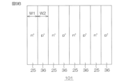
- FIG. 9A is a diagram for explaining channel formation in the semiconductor device 101 according to Condition 1.
- FIG. 9B is a diagram for explaining the arrangement pattern of the emitter region 25 and the contact region 36 of the semiconductor device 101 according to Condition 1.
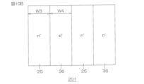
- FIG. 10A is a diagram for explaining channel formation in the semiconductor device 201 according to Condition 2.
- FIG. 10B is a diagram for explaining the arrangement pattern of the emitter region 25 and the contact region 36 of the semiconductor device 201 according to Condition 2.
- structures corresponding to the semiconductor device 1 are given the same reference numerals and the description thereof will be omitted.
- semiconductor device 101 has the same structure as semiconductor device 1.
- the emitter region 25 is formed deeper than the upper surface of the gate electrode layer 14 in the gate electrode recess 15 (the bottom wall 22 of the gate electrode recess 15). That is, the bottom portion 50 of the emitter region 25 is located in the second main region with respect to the upper surface of the gate electrode layer 14 (bottom wall 22 of the gate electrode recess 15) in the peripheral portions 9 on both sides of the first intersection region 33 in the first direction It is located on the surface 4 side (the opposite side of the first main surface 3).
- the depth D1 of the emitter region 25 from the first main surface 3 is greater than the depth D2 of the gate electrode recess 15 from the first main surface 3 (D1>D2).
- the emitter region 25 has opposing portions 40 that face the gate electrode layer 14 with the gate insulating layer 13 interposed therebetween below the peripheral portion 9 on both sides of the first intersection region 33 in the first direction X. .
- the width W1 of the emitter region 25 in the first direction X is, for example, 1.0 ⁇ m or less, and preferably 0.5 ⁇ m or more and 1.0 ⁇ m or less.
- the width W2 of the contact region 36 in the first direction X may be equal to or slightly wider than the width of the contact trench 31 in the first direction.
- emitter region 25 is formed shallower than the upper surface of gate electrode layer 14 in gate electrode recess 15 (bottom wall 22 of gate electrode recess 15).
- the bottom portion 50 of the emitter region 25 is located in the first main region relative to the upper surface of the gate electrode layer 14 (bottom wall 22 of the gate electrode recess 15) in the peripheral portions 9 on both sides of the first intersection region 33 in the first direction It is located on the surface 3 side.
- the depth D1 of the emitter region 25 from the first main surface 3 is smaller than the depth D2 of the gate electrode recess 15 from the first main surface 3 (D1 ⁇ D2).
- the width W3 of the emitter region 25 in the first direction X exceeds, for example, 1.0 ⁇ m.
- the width W4 of the contact region 36 in the first direction X may be equal to or slightly wider than the width of the contact trench 31 in the first direction.
- the width W5 of the gate electrode recess 15 in the first direction is set wider than the width W6 of the contact trench 31 in the first direction. This is to ensure a margin in consideration of positional deviation during patterning of the mask 78 for forming the contact trench 31 (see FIGS. 8L and 8M).
- the emitter contact electrode layer 51 falls within the range of the gate covering insulating layer 16, and the emitter contact electrode layer 51 is reliably insulated from the gate electrode layer 14 by the gate covering insulating layer 16. This avoids emitter-gate short circuits. That is, it is necessary to make the digging width of the gate electrode layer 14 (the width W5 of the gate electrode recess 15) wider than the contact dimension of the emitter contact electrode layer 51 (the width W6 of the contact trench 31).
- the region of the body region 8 excluding the region below the gate electrode recess 15 is a region in which a main current path can be formed in the channel formation region 202 in which a channel CH can be formed, and
- the region below the electrode recess 15 is a region in which it is difficult to form a main current path.
- the channel width tends to decrease and the on-resistance increases.
- the channel forming region 202 is shown by hatching including solid lines and broken lines.
- the width W3 of the emitter region 25 must be designed to be relatively wide in consideration of the etching margin. This is because if the width W3 of the emitter region 25 is too narrow, the portion of the emitter region 25 facing the gate electrode layer 14 will be significantly reduced after the gate electrode recess 15 is formed.
- the entire region of the body region 8 in the first direction X, including the region below the gate electrode recess 15, is the channel formation region 102 in which a main current path can be formed.
- the channel width can be increased compared to the semiconductor device 201, and the on-resistance can be reduced.
- the channel forming region 102 is shown by hatching including solid lines and broken lines.
- the width W1 of the emitter region 25 there is no need to consider the etching margin and the pattern of the gate electrode recess 15. This is because even after the gate electrode recess 15 is formed, the opposing portion 40 of the emitter region 24 can be secured below the peripheral portion 9, and thereby the channel forming region 102 having a sufficient channel width can be secured. Therefore, the width W1 of the emitter region 25 can be made narrower than the width W3 of the emitter region 25 of the semiconductor device 201.
- FIG. 11 is a graph obtained by simulation of the short circuit waveforms of the semiconductor device 101 according to condition 1 and the semiconductor device 201 according to condition 2.
- the left vertical axis is collector current IC [A]
- the right vertical axis is collector-emitter voltage VCE [V]
- the horizontal axis is time [s].
- the gate voltages under conditions 1 and 2 are shown in a broken line graph
- the collector voltages under conditions 1 and 2 are shown in a solid line graph
- the collector currents under conditions 1 and 2 are shown in a dash-dotted line graph.
- the breakdown resistance can be improved.
- FIG. 12 is a graph obtained by simulation of the current-voltage characteristics of the semiconductor device 101 according to condition 1 and the semiconductor device 201 according to condition 2.
- FIG. 13 is an enlarged view of a part of the graph of FIG. 12.
- the vertical axis is collector current IC [A]
- the horizontal axis is collector-emitter voltage VCE [V].
- FIG. 13 shows a graph in which the collector-emitter voltage VCE of FIG. 12 is in the range of 0 to 2V.
- Condition 1 the characteristics of the semiconductor device 101 according to Condition 1 are shown by a solid line graph, and the characteristics of the semiconductor device 201 according to Condition 2 are shown by a broken line graph. Both Condition 1 and Condition 2 show current-voltage characteristics when the collector-emitter voltage VCE is varied from 0V to 10V.
- the collector-emitter voltages VCE when the collector current IC is 20A, 40A, 60A, 80A, and 100A are 1.26V, 1.60V, and 1.91V, respectively. , 2.25V and 2.66V.
- the collector-emitter voltages VCE when the collector current IC is 20A, 40A, 60A, 80A, and 100A are 1.28V, 1.65V, and 2. .01V, 2.42V and 3.20V.
- the collector-emitter voltage VCE required for startup can be reduced compared to the semiconductor device 201, so that the on-loss can be reduced.
- FIG. 14 is a graph obtained by simulation of the current-voltage characteristics of the semiconductor device 101 according to condition 1 and the semiconductor device 201 according to condition 2.
- the vertical axis is collector current IC [A]
- the horizontal axis is gate-emitter voltage VGE [V].
- the characteristics of the semiconductor device 101 according to Condition 1 are shown by a solid line graph
- the characteristics of the semiconductor device 201 according to Condition 2 are shown by a broken line graph. Both Condition 1 and Condition 2 show current-voltage characteristics when the gate-emitter voltage VGE is changed from 0V to 15V.
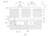
- FIG. 15 is a schematic cross-sectional perspective view showing a partial region of a semiconductor device 81 according to a second embodiment of the present disclosure.
- FIG. 16 is a schematic cross-sectional view showing a part of the semiconductor device 81 of FIG. 15.
- FIG. 17 is a schematic cross-sectional view showing a part of the semiconductor device 81 of FIG. 15.
- the gate electrode layer 14 has an uneven structure including a plurality of gate electrode recesses 15.
- the gate electrode layer 14 has a flat structure in which the depth position of the upper surface 82 is constant throughout. More specifically, with reference to FIGS. 16 and 17, the upper surface 82 of the gate electrode layer 14 is located in a region between the first main surface 3 and the bottom 50 of the emitter region 25 with respect to the normal direction Z. ing.
- the emitter region 25 similarly to the semiconductor device 1, the emitter region 25 has a facing portion 40 that faces the gate electrode layer 14 with the gate insulating layer 13 interposed therebetween in the vicinity of the first intersection region 33 in the first direction X. There is.
- the gate covering insulating layer 16 has an integral structure extending across the plurality of contact trenches 31 along the first direction X.
- the gate covering insulating layer 16 has an insulating layer uneven structure formed by insulating layer recesses 83 formed in the first intersection region 33 of each contact trench 31 .
- Emitter contact electrode layer 51 is embedded in insulating layer recess 83 .
- the gate covering insulating layer 16 has a base portion 85 having a flat lower surface 84 in contact with the upper surface 82 of the gate electrode layer 14 along the first direction A convex portion 86 protruding from the portion 85 may be included.
- the uneven structure of the gate covering insulating layer 16 is formed by alternately arranging convex portions 86 and insulating layer concave portions 83 along the first direction X.
- the semiconductor device 81 can also achieve the same effects as those described for the semiconductor device 1.
- the entire region of the body region 8 in the first direction X can be used as the channel formation region 102 in which the channel CH can be formed.
- the semiconductor device 81 when etching the first base conductor layer 74 in the method for manufacturing the semiconductor device 1 (see FIG. 8F), the first base conductor layer 74 is etched without patterning. It can be manufactured by digging almost the entire surface.
- FIG. 18 is a schematic cross-sectional perspective view showing a partial region of a semiconductor device 91 according to a third embodiment of the present disclosure.
- structures corresponding to those described for the semiconductor device 1 will be given the same reference numerals and descriptions will be omitted.
- the semiconductor device 1 described above an example has been described in which the p-type collector region 5 is formed on the surface portion of the second main surface 4.
- an n-type drain region 92 is formed on the surface portion of the second main surface 4 instead of the p-type collector region 5 .
- the semiconductor device 91 has a basic configuration including a trench gate type MISFET (Metal Insulator Semiconductor Field Effect Transistor).
- MISFET Metal Insulator Semiconductor Field Effect Transistor
- the semiconductor device 91 can also achieve the same effects as those described for the semiconductor device 1.
- the semiconductor device 91 can be manufactured by simply forming an n-type drain region 92 in place of the p-type collector region 5 and changing the layout of each mask in the method for manufacturing the semiconductor device 1.
- a structure may be adopted in which the conductivity type of each semiconductor portion is inverted. That is, the p-type portion may be made into the n-type, and the n-type portion may be made into the p-type.
- chip 2 is made of silicon single crystal.
- chip 2 may also include SiC.
- the chip 2 may be made of SiC single crystal.
- the gate trench (12) includes an intersection region (33) that intersects with the gate trench (12), and extends from the intersection region (33) to the gate trench (12) along a second direction (Y) that intersects the first direction (X).
- a spatial region (15) is formed above the gate electrode (14) at least in the crossing region (33) and a peripheral portion (9) of the crossing region (33) in the gate trench (12), The spatial region (15) covers the upper surface (22) of the gate electrode (14) in the intersection region (33) and the periphery (9) of the intersection region (33), and the gate electrode (14) and a covering insulating layer (16) that insulates between the contact electrode (51) and the contact electrode (51),
- the first impurity region (25) is formed deeper than the upper surface (22) of the gate electrode (14) in the peripheral portion (9) of the intersection region (33). , 101).
- the first impurity region (25) has a facing portion (40) facing the gate electrode (14) below the peripheral portion (9) of the crossing region (33).
- the contact electrode (51) is connected to the body region (8) at the bottom wall of the contact trench (31), and connected to the first impurity region (25) at the side wall of the contact trench (31). , the semiconductor device (1, 81, 91, 101) according to Supplementary Note 1-1 or Supplementary Note 1-2.
- the peripheral part (9) of the intersection area (33) includes an area within a range of 0.05 ⁇ m or more and 0.5 ⁇ m or less from the intersection area (33), according to any one of Supplementary notes 1-1 to 1-5. (1, 81, 91, 101).
- the gate electrode (14) is a gate formed in the intersection region (33) of each contact trench (31) and the peripheral portion (9) of the intersection region (33) along the first direction (X). It has an electrode uneven structure formed by an electrode recess (15),
- the semiconductor device (1, 91, 101) according to any one of Supplementary notes 1-1 to 1-6, wherein the covering insulating layer (16) is embedded in the gate electrode recess (15).
- the gate electrode recess (15) is formed across a peripheral portion (9) on one side and a peripheral portion (9) on the other side of the intersection region (33) in the first direction (X),
- the covering insulating layer (16) includes a first portion (47) disposed in the intersection region (33) and a peripheral portion on one side in the first direction (X) with respect to the first portion (47). (9) and a second portion (48) disposed in each of the peripheral portions (9) on the other side (1, 91, 101). ).
- the width (W6) of the contact trench (31) in the first direction (X) is 0.3 ⁇ m or more and 1.0 ⁇ m or less, Side walls of the gate electrode recess (15) are formed on both sides of the contact trench (31) in the first direction (X) with an interval of 0.05 ⁇ m or more and 0.5 ⁇ m or less.
- the semiconductor device (1, 91, 101) according to any one of 1-7 to Supplementary Note 1-9.
- the covering insulating layer (16) has an integral structure extending across the plurality of contact trenches (31) along the first direction (X), and has an integral structure extending across the plurality of contact trenches (31). It has an insulating layer uneven structure formed by insulating layer recesses (83) formed in the region (33), The semiconductor device (81) according to appendix 1-11, wherein the contact electrode (51) is embedded in the insulating layer recess (83).
- the covering insulating layer (16) is adjacent to a base portion (85) having a flat lower surface (84) in contact with the upper surface (82) of the gate electrode (14) along the first direction (X). a convex portion (86) protruding from the base portion (85) between the insulating layer concave portions (83); Supplementary note 1-12, wherein the insulating layer uneven structure is formed by alternately arranging the convex portions (86) and the insulating layer concave portions (83) along the first direction (X).
- the first impurity region (25) includes an emitter region (25), The semiconductor device (1, 81, 101) according to any one of Appendixes 1-1 to 1-13, wherein the contact electrode (51) includes an emitter contact electrode (51).
- the first impurity region (25) includes a source region (25), The semiconductor device (91) according to any one of Appendixes 1-1 to 1-13, wherein the contact electrode (51) includes a source contact electrode (51).
Landscapes
- Electrodes Of Semiconductors (AREA)
Priority Applications (2)
| Application Number | Priority Date | Filing Date | Title |
|---|---|---|---|
| JP2024545581A JPWO2024053457A1 (https=) | 2022-09-09 | 2023-08-28 | |
| CN202380064158.2A CN119856587A (zh) | 2022-09-09 | 2023-08-28 | 半导体装置 |
Applications Claiming Priority (2)
| Application Number | Priority Date | Filing Date | Title |
|---|---|---|---|
| JP2022143916 | 2022-09-09 | ||
| JP2022-143916 | 2022-09-09 |
Publications (1)
| Publication Number | Publication Date |
|---|---|
| WO2024053457A1 true WO2024053457A1 (ja) | 2024-03-14 |
Family
ID=90191242
Family Applications (1)
| Application Number | Title | Priority Date | Filing Date |
|---|---|---|---|
| PCT/JP2023/030991 Ceased WO2024053457A1 (ja) | 2022-09-09 | 2023-08-28 | 半導体装置 |
Country Status (4)
| Country | Link |
|---|---|
| US (1) | US20250203898A1 (https=) |
| JP (1) | JPWO2024053457A1 (https=) |
| CN (1) | CN119856587A (https=) |
| WO (1) | WO2024053457A1 (https=) |
Citations (4)
| Publication number | Priority date | Publication date | Assignee | Title |
|---|---|---|---|---|
| JP2001015743A (ja) * | 1999-06-30 | 2001-01-19 | Toshiba Corp | 半導体装置及びその製造方法 |
| JP2003303967A (ja) * | 2002-04-09 | 2003-10-24 | Shindengen Electric Mfg Co Ltd | 半導体装置およびその製造方法 |
| JP2018166169A (ja) * | 2017-03-28 | 2018-10-25 | エイブリック株式会社 | 半導体装置 |
| WO2019103135A1 (ja) * | 2017-11-24 | 2019-05-31 | ローム株式会社 | 半導体装置 |
-
2023
- 2023-08-28 WO PCT/JP2023/030991 patent/WO2024053457A1/ja not_active Ceased
- 2023-08-28 CN CN202380064158.2A patent/CN119856587A/zh active Pending
- 2023-08-28 JP JP2024545581A patent/JPWO2024053457A1/ja active Pending
-
2025
- 2025-03-07 US US19/073,077 patent/US20250203898A1/en active Pending
Patent Citations (4)
| Publication number | Priority date | Publication date | Assignee | Title |
|---|---|---|---|---|
| JP2001015743A (ja) * | 1999-06-30 | 2001-01-19 | Toshiba Corp | 半導体装置及びその製造方法 |
| JP2003303967A (ja) * | 2002-04-09 | 2003-10-24 | Shindengen Electric Mfg Co Ltd | 半導体装置およびその製造方法 |
| JP2018166169A (ja) * | 2017-03-28 | 2018-10-25 | エイブリック株式会社 | 半導体装置 |
| WO2019103135A1 (ja) * | 2017-11-24 | 2019-05-31 | ローム株式会社 | 半導体装置 |
Also Published As
| Publication number | Publication date |
|---|---|
| US20250203898A1 (en) | 2025-06-19 |
| CN119856587A (zh) | 2025-04-18 |
| JPWO2024053457A1 (https=) | 2024-03-14 |
Similar Documents
| Publication | Publication Date | Title |
|---|---|---|
| JP6477885B2 (ja) | 半導体装置および半導体装置の製造方法 | |
| JP7540034B2 (ja) | 半導体装置 | |
| JP4754353B2 (ja) | 縦型トレンチゲート半導体装置およびその製造方法 | |
| JP6666671B2 (ja) | 半導体装置 | |
| US20210242342A1 (en) | Semiconductor device and method for manufacturing same | |
| CN112673466B (zh) | 半导体装置 | |
| CN117423733A (zh) | 半导体装置 | |
| WO2014136802A1 (ja) | 半導体装置 | |
| JPH0817233B2 (ja) | 絶縁ゲート型バイポーラトランジスタ | |
| CN108695390B (zh) | 半导体器件及其制造方法 | |
| US12288817B2 (en) | Semiconductor device and method for manufacturing the same | |
| JP2005268679A (ja) | 半導体装置およびその製造方法 | |
| US20240387648A1 (en) | Semiconductor device | |
| US20240282762A1 (en) | Semiconductor device and method of manufacturing semiconductor device | |
| JP4735235B2 (ja) | 絶縁ゲート型半導体装置およびその製造方法 | |
| US20240297071A1 (en) | Semiconductor device and method of manufacturing semiconductor device | |
| JP4623656B2 (ja) | 縦型ゲート半導体装置およびその製造方法 | |
| WO2024053457A1 (ja) | 半導体装置 | |
| KR102627999B1 (ko) | 전력 반도체 소자 제조 방법 | |
| JP3646343B2 (ja) | 半導体装置の製造方法 | |
| JP2023113080A (ja) | 半導体装置および半導体装置の製造方法 | |
| KR20050009797A (ko) | 셀로우 트렌치 소자 분리막을 갖는 고전압 트랜지스터의구조 | |
| WO2024053456A1 (ja) | 半導体装置および半導体装置の製造方法 | |
| US20240304682A1 (en) | Semiconductor device and method of manufacturing semiconductor device | |
| US20260047154A1 (en) | Silicon carbide semiconductor device |
Legal Events
| Date | Code | Title | Description |
|---|---|---|---|
| 121 | Ep: the epo has been informed by wipo that ep was designated in this application |
Ref document number: 23862996 Country of ref document: EP Kind code of ref document: A1 |
|
| WWE | Wipo information: entry into national phase |
Ref document number: 2024545581 Country of ref document: JP |
|
| WWE | Wipo information: entry into national phase |
Ref document number: 202380064158.2 Country of ref document: CN |
|
| NENP | Non-entry into the national phase |
Ref country code: DE |
|
| WWP | Wipo information: published in national office |
Ref document number: 202380064158.2 Country of ref document: CN |
|
| 122 | Ep: pct application non-entry in european phase |
Ref document number: 23862996 Country of ref document: EP Kind code of ref document: A1 |