WO2024053457A1 - Semiconductor device - Google Patents
Semiconductor device Download PDFInfo
- Publication number
- WO2024053457A1 WO2024053457A1 PCT/JP2023/030991 JP2023030991W WO2024053457A1 WO 2024053457 A1 WO2024053457 A1 WO 2024053457A1 JP 2023030991 W JP2023030991 W JP 2023030991W WO 2024053457 A1 WO2024053457 A1 WO 2024053457A1
- Authority
- WO
- WIPO (PCT)
- Prior art keywords
- region
- contact
- trench
- gate
- semiconductor device
- Prior art date
Links
- 239000004065 semiconductor Substances 0.000 title claims abstract description 127
- 230000002093 peripheral effect Effects 0.000 claims abstract description 39
- 210000000746 body region Anatomy 0.000 claims description 43
- 239000012535 impurity Substances 0.000 claims description 40
- 239000011248 coating agent Substances 0.000 abstract 1
- 238000000576 coating method Methods 0.000 abstract 1
- 238000009413 insulation Methods 0.000 abstract 1
- 239000010410 layer Substances 0.000 description 235
- 238000000034 method Methods 0.000 description 31
- 238000010586 diagram Methods 0.000 description 27
- 239000011229 interlayer Substances 0.000 description 21
- 238000005468 ion implantation Methods 0.000 description 15
- 238000003860 storage Methods 0.000 description 12
- 239000004020 conductor Substances 0.000 description 11
- 238000005530 etching Methods 0.000 description 11
- 230000015572 biosynthetic process Effects 0.000 description 10
- 238000005229 chemical vapour deposition Methods 0.000 description 7
- 238000004088 simulation Methods 0.000 description 6
- VYPSYNLAJGMNEJ-UHFFFAOYSA-N Silicium dioxide Chemical compound O=[Si]=O VYPSYNLAJGMNEJ-UHFFFAOYSA-N 0.000 description 5
- XUIMIQQOPSSXEZ-UHFFFAOYSA-N Silicon Chemical compound [Si] XUIMIQQOPSSXEZ-UHFFFAOYSA-N 0.000 description 5
- 239000013078 crystal Substances 0.000 description 5
- 238000004519 manufacturing process Methods 0.000 description 5
- 229910052710 silicon Inorganic materials 0.000 description 5
- 239000010703 silicon Substances 0.000 description 5
- 229910052814 silicon oxide Inorganic materials 0.000 description 5
- 238000001039 wet etching Methods 0.000 description 5
- 230000015556 catabolic process Effects 0.000 description 3
- 238000004518 low pressure chemical vapour deposition Methods 0.000 description 3
- 230000003647 oxidation Effects 0.000 description 3
- 238000007254 oxidation reaction Methods 0.000 description 3
- 238000000059 patterning Methods 0.000 description 3
- 229910021420 polycrystalline silicon Inorganic materials 0.000 description 3
- 229920005591 polysilicon Polymers 0.000 description 3
- 229910004298 SiO 2 Inorganic materials 0.000 description 2
- 238000001312 dry etching Methods 0.000 description 2
- 230000000694 effects Effects 0.000 description 2
- 239000011521 glass Substances 0.000 description 2
- 230000012447 hatching Effects 0.000 description 2
- 239000000758 substrate Substances 0.000 description 2
- OAICVXFJPJFONN-UHFFFAOYSA-N Phosphorus Chemical compound [P] OAICVXFJPJFONN-UHFFFAOYSA-N 0.000 description 1
- 229910052581 Si3N4 Inorganic materials 0.000 description 1
- RTAQQCXQSZGOHL-UHFFFAOYSA-N Titanium Chemical compound [Ti] RTAQQCXQSZGOHL-UHFFFAOYSA-N 0.000 description 1
- HIVGXUNKSAJJDN-UHFFFAOYSA-N [Si].[P] Chemical compound [Si].[P] HIVGXUNKSAJJDN-UHFFFAOYSA-N 0.000 description 1
- 230000004888 barrier function Effects 0.000 description 1
- 230000005669 field effect Effects 0.000 description 1
- 239000012212 insulator Substances 0.000 description 1
- 229910052751 metal Inorganic materials 0.000 description 1
- 239000002184 metal Substances 0.000 description 1
- 150000004767 nitrides Chemical class 0.000 description 1
- 230000001590 oxidative effect Effects 0.000 description 1
- 229910052698 phosphorus Inorganic materials 0.000 description 1
- 239000011574 phosphorus Substances 0.000 description 1
- 238000005498 polishing Methods 0.000 description 1
- 230000007261 regionalization Effects 0.000 description 1
- HQVNEWCFYHHQES-UHFFFAOYSA-N silicon nitride Chemical compound N12[Si]34N5[Si]62N3[Si]51N64 HQVNEWCFYHHQES-UHFFFAOYSA-N 0.000 description 1
- 239000000126 substance Substances 0.000 description 1
- 239000010936 titanium Substances 0.000 description 1
- 229910052719 titanium Inorganic materials 0.000 description 1
- WFKWXMTUELFFGS-UHFFFAOYSA-N tungsten Chemical compound [W] WFKWXMTUELFFGS-UHFFFAOYSA-N 0.000 description 1
- 229910052721 tungsten Inorganic materials 0.000 description 1
- 239000010937 tungsten Substances 0.000 description 1
- 238000009279 wet oxidation reaction Methods 0.000 description 1
Images


Classifications
-
- H—ELECTRICITY
- H01—ELECTRIC ELEMENTS
- H01L—SEMICONDUCTOR DEVICES NOT COVERED BY CLASS H10
- H01L29/00—Semiconductor devices adapted for rectifying, amplifying, oscillating or switching, or capacitors or resistors with at least one potential-jump barrier or surface barrier, e.g. PN junction depletion layer or carrier concentration layer; Details of semiconductor bodies or of electrodes thereof ; Multistep manufacturing processes therefor
- H01L29/40—Electrodes ; Multistep manufacturing processes therefor
- H01L29/41—Electrodes ; Multistep manufacturing processes therefor characterised by their shape, relative sizes or dispositions
- H01L29/417—Electrodes ; Multistep manufacturing processes therefor characterised by their shape, relative sizes or dispositions carrying the current to be rectified, amplified or switched
-
- H—ELECTRICITY
- H01—ELECTRIC ELEMENTS
- H01L—SEMICONDUCTOR DEVICES NOT COVERED BY CLASS H10
- H01L29/00—Semiconductor devices adapted for rectifying, amplifying, oscillating or switching, or capacitors or resistors with at least one potential-jump barrier or surface barrier, e.g. PN junction depletion layer or carrier concentration layer; Details of semiconductor bodies or of electrodes thereof ; Multistep manufacturing processes therefor
- H01L29/40—Electrodes ; Multistep manufacturing processes therefor
- H01L29/41—Electrodes ; Multistep manufacturing processes therefor characterised by their shape, relative sizes or dispositions
- H01L29/423—Electrodes ; Multistep manufacturing processes therefor characterised by their shape, relative sizes or dispositions not carrying the current to be rectified, amplified or switched
-
- H—ELECTRICITY
- H01—ELECTRIC ELEMENTS
- H01L—SEMICONDUCTOR DEVICES NOT COVERED BY CLASS H10
- H01L29/00—Semiconductor devices adapted for rectifying, amplifying, oscillating or switching, or capacitors or resistors with at least one potential-jump barrier or surface barrier, e.g. PN junction depletion layer or carrier concentration layer; Details of semiconductor bodies or of electrodes thereof ; Multistep manufacturing processes therefor
- H01L29/40—Electrodes ; Multistep manufacturing processes therefor
- H01L29/43—Electrodes ; Multistep manufacturing processes therefor characterised by the materials of which they are formed
- H01L29/49—Metal-insulator-semiconductor electrodes, e.g. gates of MOSFET
-
- H—ELECTRICITY
- H01—ELECTRIC ELEMENTS
- H01L—SEMICONDUCTOR DEVICES NOT COVERED BY CLASS H10
- H01L29/00—Semiconductor devices adapted for rectifying, amplifying, oscillating or switching, or capacitors or resistors with at least one potential-jump barrier or surface barrier, e.g. PN junction depletion layer or carrier concentration layer; Details of semiconductor bodies or of electrodes thereof ; Multistep manufacturing processes therefor
- H01L29/66—Types of semiconductor device ; Multistep manufacturing processes therefor
- H01L29/66007—Multistep manufacturing processes
- H01L29/66075—Multistep manufacturing processes of devices having semiconductor bodies comprising group 14 or group 13/15 materials
- H01L29/66227—Multistep manufacturing processes of devices having semiconductor bodies comprising group 14 or group 13/15 materials the devices being controllable only by the electric current supplied or the electric potential applied, to an electrode which does not carry the current to be rectified, amplified or switched, e.g. three-terminal devices
- H01L29/66409—Unipolar field-effect transistors
- H01L29/66477—Unipolar field-effect transistors with an insulated gate, i.e. MISFET
-
- H—ELECTRICITY
- H01—ELECTRIC ELEMENTS
- H01L—SEMICONDUCTOR DEVICES NOT COVERED BY CLASS H10
- H01L29/00—Semiconductor devices adapted for rectifying, amplifying, oscillating or switching, or capacitors or resistors with at least one potential-jump barrier or surface barrier, e.g. PN junction depletion layer or carrier concentration layer; Details of semiconductor bodies or of electrodes thereof ; Multistep manufacturing processes therefor
- H01L29/66—Types of semiconductor device ; Multistep manufacturing processes therefor
- H01L29/68—Types of semiconductor device ; Multistep manufacturing processes therefor controllable by only the electric current supplied, or only the electric potential applied, to an electrode which does not carry the current to be rectified, amplified or switched
- H01L29/70—Bipolar devices
- H01L29/72—Transistor-type devices, i.e. able to continuously respond to applied control signals
- H01L29/739—Transistor-type devices, i.e. able to continuously respond to applied control signals controlled by field-effect, e.g. bipolar static induction transistors [BSIT]
-
- H—ELECTRICITY
- H01—ELECTRIC ELEMENTS
- H01L—SEMICONDUCTOR DEVICES NOT COVERED BY CLASS H10
- H01L29/00—Semiconductor devices adapted for rectifying, amplifying, oscillating or switching, or capacitors or resistors with at least one potential-jump barrier or surface barrier, e.g. PN junction depletion layer or carrier concentration layer; Details of semiconductor bodies or of electrodes thereof ; Multistep manufacturing processes therefor
- H01L29/66—Types of semiconductor device ; Multistep manufacturing processes therefor
- H01L29/68—Types of semiconductor device ; Multistep manufacturing processes therefor controllable by only the electric current supplied, or only the electric potential applied, to an electrode which does not carry the current to be rectified, amplified or switched
- H01L29/76—Unipolar devices, e.g. field effect transistors
- H01L29/772—Field effect transistors
- H01L29/78—Field effect transistors with field effect produced by an insulated gate
Definitions
- the present disclosure relates to a semiconductor device.
- Patent Document 1 discloses a semiconductor layer having a main surface in which a trench is formed, a body region of a first conductivity type formed along a sidewall of the trench in a surface portion of the main surface of the semiconductor layer, and a body region of the body. a second conductivity type impurity region formed along the sidewalls of the trench in the surface portion of the region; a gate insulating layer formed on the inner wall of the trench; and an impurity region buried in the trench and sandwiching the gate insulating layer.
- a semiconductor device is disclosed, including a contact electrode connected to the trench, and a buried insulating layer interposed between the gate electrode and the contact electrode in the trench and insulating the gate electrode and the contact electrode.
- An embodiment of the present disclosure provides a semiconductor device that can improve the degree of freedom in designing dimensions of first impurity regions such as an emitter region and a source region, thereby improving breakdown resistance.
- An embodiment of the present disclosure provides a semiconductor device that can suppress reduction in channel width and reduce on-resistance in a structure including a contact trench that intersects with a gate trench.
- a semiconductor device includes a chip having a first main surface in which a gate trench extending in a first direction having a bottom wall and a side wall is formed, and the gate trench is formed in a surface portion of the first main surface.
- a body region of a first conductivity type formed along the sidewall of the gate trench;
- a first impurity region of a second conductivity type formed along the sidewall of the gate trench in a surface portion of the body region;
- a gate insulating layer formed on the bottom wall and the side wall of the trench, a gate electrode embedded in the gate trench and facing the body region and the first impurity region with the gate insulating layer in between, and the gate trench.
- a contact trench that includes an intersection region that intersects with the first direction, and is drawn out from the intersection region to the outside of the gate trench along a second direction that intersects with the first direction; a contact electrode electrically connected to the body region and the first impurity region, and a space region is formed on the gate electrode in at least the crossing region and a peripheral portion of the crossing region in the gate trench.
- a covering insulating layer is embedded in the spatial region to cover the upper surface of the gate electrode in the intersection region and a peripheral portion of the intersection region, and to insulate between the gate electrode and the contact electrode.
- the first impurity region is formed deeper than the upper surface of the gate electrode in a peripheral portion of the intersection region.
- the first impurity region is formed deeper than the upper surface of the gate electrode in the peripheral portion of the intersection region. Therefore, a channel can be formed in the periphery of the intersection region, so that reduction in channel width can be suppressed and on-resistance can be reduced.
- the first impurity region is formed deeper than the upper surface of the gate electrode. This allows a channel to be formed also in the lower region around the intersection region. Therefore, there is no need to consider the patterning margin during etching or contact pattern formation, and the degree of freedom in designing the dimensions of the first impurity region can be improved, thereby improving the breakdown resistance.
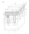
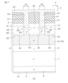
- FIG. 1 is a schematic cross-sectional perspective view showing a partial region of a semiconductor device according to a first embodiment of the present disclosure.
- FIG. 2 is a diagram in which the structure on the first main surface of the chip is removed from FIG. 1.
- FIG. 3 is a diagram from FIG. 2 with the emitter contact electrode layer removed.
- FIG. 4 is a schematic plan view of FIG. 3 viewed from the first main surface of the chip.
- FIG. 5 is a sectional view taken along the line VV shown in FIG. 4.
- FIG. 6 is a cross-sectional view taken along line VI-VI shown in FIG. 4.
- FIG. 7 is a cross-sectional view taken along line VII-VII shown in FIG. 4.
- FIG. 8A is a diagram illustrating an example of a method for manufacturing the semiconductor device.
- FIG. 8A is a diagram illustrating an example of a method for manufacturing the semiconductor device.
- FIG. 8B is a diagram showing a step after FIG. 8A.
- FIG. 8C is a diagram showing a step after FIG. 8B.
- FIG. 8D is a diagram showing a step after FIG. 8C.
- FIG. 8E is a diagram showing a step after FIG. 8D.
- FIG. 8F is a diagram showing a step after FIG. 8E.
- FIG. 8G is a diagram showing a step after FIG. 8F.
- FIG. 8H is a diagram showing a step after FIG. 8G.
- FIG. 8I is a diagram showing a step after FIG. 8H.
- FIG. 8J is a diagram showing a step after FIG. 8I.
- FIG. 8K is a diagram showing a step after FIG. 8J.
- FIG. 8L is a diagram showing a step after FIG. 8K.
- FIG. 8M is a diagram showing a step after FIG. 8L.
- FIG. 8N is a diagram showing a step after FIG. 8M.
- FIG. 9A is a diagram for explaining channel formation in a semiconductor device according to condition 1.
- FIG. 9B is a diagram for explaining the arrangement pattern of the emitter region and contact region of the semiconductor device according to Condition 1.
- FIG. 10A is a diagram for explaining channel formation in a semiconductor device according to Condition 2.
- FIG. 10B is a diagram for explaining the arrangement pattern of the emitter region and contact region of the semiconductor device according to Condition 2.
- FIG. 11 is a graph obtained by simulation of short-circuit waveforms of the semiconductor device according to Conditions 1 and 2.
- FIG. 12 is a graph obtained by simulation of the current-voltage characteristics of the semiconductor device according to Conditions 1 and 2.
- FIG. 13 is an enlarged view of a part of the graph of FIG. 12.
- FIG. 14 is a graph obtained by simulation of the current-voltage characteristics of the semiconductor device according to Conditions 1 and 2.
- FIG. 15 is a schematic cross-sectional perspective view showing a partial region of a semiconductor device according to a second embodiment of the present disclosure.
- FIG. 16 is a schematic cross-sectional view showing a part of the semiconductor device of FIG. 15.
- FIG. 17 is a schematic cross-sectional view showing a part of the semiconductor device of FIG. 15.
- FIG. 18 is a schematic cross-sectional perspective view showing a partial region of a semiconductor device according to a third embodiment of the present disclosure.
- FIG. 1 is a schematic cross-sectional perspective view showing a partial region of a semiconductor device 1 according to a first embodiment of the present disclosure.
- FIG. 2 is a diagram in which the structure on the first main surface 3 of the chip 2 is removed from FIG. 1.
- FIG. 3 is a diagram from FIG. 2 with the emitter contact electrode layer 51 removed.
- FIG. 4 is a schematic plan view of FIG. 3 viewed from the first main surface 3 of the chip 2.
- FIG. 5 is a sectional view taken along the line VV shown in FIG. 4.
- FIG. 6 is a cross-sectional view taken along line VI-VI shown in FIG. 4.
- FIG. 7 is a cross-sectional view taken along line VII-VII shown in FIG. 4. 5 to 7 also illustrate the structure on the first main surface 3 of the chip 2.
- the semiconductor device 1 has a basic configuration including a trench gate type IGBT (Insulated Gate Bipolar Transistor).
- semiconductor device 1 includes an n ⁇ type chip 2.
- the chip 2 is made of an n - type silicon single crystal substrate.
- the silicon single crystal substrate is formed using an n ⁇ type silicon single crystal semiconductor wafer manufactured through the FZ (Floating Zone) method.
- the chip 2 may be called a semiconductor chip or a semiconductor layer.
- the chip 2 has a first main surface 3 on one side and a second main surface 4 on the other side.
- the thickness of the chip 2 may be 50 ⁇ m or more and 300 ⁇ m or less.
- the thickness of the chip 2 may be 50 ⁇ m or more and 100 ⁇ m or less, 100 ⁇ m or more and 150 ⁇ m or less, 150 ⁇ m or more and 200 ⁇ m or less, 200 ⁇ m or more and 250 ⁇ m or less, or 250 ⁇ m or more and 300 ⁇ m or less.
- a p-type collector region 5 is formed on the surface portion of the second main surface 4.
- An n-type charge storage region 6 is formed in the surface portion of the first main surface 3 .
- the charge storage region 6 is formed at a distance from the collector region 5 on the first main surface 3 side.
- an n ⁇ type drift region 7 is formed in a region between the collector region 5 and the charge storage region 6.
- Drift region 7 is formed by a region located between collector region 5 and charge storage region 6 in chip 2 .
- a p-type body region 8 is formed on the surface of the charge storage region 6 .
- a plurality of trench gate electrode structures 10 and a plurality of trench emitter electrode structures 11 are formed at intervals on the surface portion of the first main surface 3.
- FIGS. 1 to 7 only one trench gate electrode structure 10 and one trench emitter electrode structure 11 adjacent to each other are shown.
- the structure of the semiconductor device 1 will be described below, focusing on the structure of one trench gate electrode structure 10 and one trench emitter electrode structure 11.
- the trench gate electrode structure 10 and the trench emitter electrode structure 11 extend in a band shape along an arbitrary first direction X in plan view.
- the trench gate electrode structure 10 and the trench emitter electrode structure 11 are formed at intervals along a second direction Y that intersects the first direction X.
- planar view refers to a planar view seen from the normal direction Z of the first principal surface 3 (hereinafter simply referred to as "normal direction Z"). More specifically, the second direction Y is a direction perpendicular to the first direction X. The first direction X and the second direction Y are also tangential directions of the first main surface 3.
- the trench pitch P0 between the trench gate electrode structure 10 and the trench emitter electrode structure 11 may be 0.1 ⁇ m or more and less than 0.6 ⁇ m.
- Trench pitch P0 is 0.1 ⁇ m or more and 0.2 ⁇ m or less, 0.2 ⁇ m or more and 0.3 ⁇ m or less, 0.3 ⁇ m or more and 0.4 ⁇ m or less, 0.4 ⁇ m or more and 0.5 ⁇ m or less, or 0.5 ⁇ m or more and 0.6 ⁇ m It may be less than
- the trench pitch P0 is preferably 0.2 ⁇ m or more and 0.4 ⁇ m or less (for example, about 0.25 ⁇ m).
- the trench gate electrode structure 10 includes a gate trench 12 , a gate insulating layer 13 , a gate electrode layer 14 , a plurality of gate electrode recesses 15 (space regions), and a plurality of gate covering insulating layers 16 .
- Gate trench 12 extends from first main surface 3 through body region 8 and charge storage region 6 to drift region 7 .
- the depth of the gate trench 12 may be 2.0 ⁇ m or more and 4.0 ⁇ m or less.
- the depth of the gate trench 12 may be 2.0 ⁇ m or more and 2.5 ⁇ m or less, 2.5 ⁇ m or more and 3.0 ⁇ m or less, 3.0 ⁇ m or more and 3.5 ⁇ m or less, or 3.5 ⁇ m or more and 4.0 ⁇ m or less.
- the depth of the gate trench 12 is preferably 2.5 ⁇ m or more and 3.5 ⁇ m or less (for example, about 3.0 ⁇ m).
- the width of the gate trench 12 in the second direction may be 0.5 ⁇ m or more and 1.5 ⁇ m or less.
- the width of the gate trench 12 in the second direction is 0.5 ⁇ m or more and 0.75 ⁇ m or less, 0.75 ⁇ m or more and 1.0 ⁇ m or less, 1.0 ⁇ m or more and 1.25 ⁇ m or less, or 1.25 ⁇ m or more and 1.5 ⁇ m or less. Good too.
- the width of the gate trench 12 in the second direction is preferably 0.5 ⁇ m or more and 1.0 ⁇ m or less (for example, about 0.75 ⁇ m).
- the gate insulating layer 13 may be formed of silicon oxide.
- the gate insulating layer 13 is formed in a film shape along the inner wall of the gate trench 12 .
- Gate insulating layer 13 defines a concave space within gate trench 12 .
- the gate electrode layer 14 may be formed of conductive polysilicon. Gate electrode layer 14 is controlled by gate voltage. The gate electrode layer 14 is embedded in the gate trench 12 with the gate insulating layer 13 in between. More specifically, the gate electrode layer 14 is embedded in a concave space defined by the gate insulating layer 13 within the gate trench 12 . The upper end of the gate electrode layer 14 is located on the first main surface 3 side with respect to the bottom of the body region 8 .
- the plurality of gate electrode recesses 15 are formed on the main surface of the gate electrode layer 14 at intervals along the first direction X.
- the upper end portion of the gate electrode layer 14 has an uneven structure including a plurality of gate electrode recesses 15.
- the interval between the plurality of gate electrode recesses 15 adjacent to each other may be greater than 0 ⁇ m and less than or equal to 10 ⁇ m.
- the interval between the plurality of gate electrode recesses 15 adjacent to each other is also the width in the first direction X of a portion of the gate electrode layer 14 sandwiched between two gate electrode recesses 15 adjacent to each other.
- the interval between the plurality of gate electrode recesses 15 adjacent to each other may be more than 0 ⁇ m and less than 2 ⁇ m, more than 2 ⁇ m and less than 4 ⁇ m, more than 4 ⁇ m and less than 6 ⁇ m, more than 6 ⁇ m and less than 8 ⁇ m, or more than 8 ⁇ m and less than 10 ⁇ m.
- each gate electrode recess 15 are formed by the gate insulating layer 13 and the gate electrode layer 14.
- the bottom wall 22 of each gate electrode recess 15 is formed of the gate electrode layer 14. Referring to FIGS. 6 and 7, the bottom wall 22 of each gate electrode recess 15 is located in a region between the first main surface 3 and the bottom 50 of the emitter region 25 (described later) with respect to the normal direction Z. There is.
- each gate electrode recess 15 is formed in a tapered shape with a bottom area smaller than the opening area.
- the angle ⁇ formed by the main surface of the gate electrode layer 14 and the side wall of the gate electrode recess 15 within the gate electrode layer 14 may be more than 90° and less than or equal to 105° (for example, about 102°).
- the plurality of gate covering insulating layers 16 are each embedded in the upper end portion of the gate electrode layer 14 within the gate trench 12. More specifically, the gate covering insulating layer 16 is embedded independently in each gate electrode recess 15. Each gate covering insulating layer 16 is exposed through the opening of the gate trench 12.
- the trench emitter electrode structure 11 includes an emitter trench 17, an emitter insulating layer 18, an emitter electrode layer 19, an emitter electrode recess 20, and an emitter covering insulating layer 21.
- Emitter trench 17 extends from first main surface 3 through body region 8 and charge storage region 6 to drift region 7 .
- the depth of the emitter trench 17 may be 2.0 ⁇ m or more and 4.0 ⁇ m or less.
- the depth of the emitter trench 17 may be 2.0 ⁇ m or more and 2.5 ⁇ m or less, 2.5 ⁇ m or more and 3.0 ⁇ m or less, 3.0 ⁇ m or more and 3.5 ⁇ m or less, or 3.5 ⁇ m or more and 4.0 ⁇ m or less.
- the depth of the emitter trench 17 is preferably 2.5 ⁇ m or more and 3.5 ⁇ m or less (for example, about 3.0 ⁇ m).
- the depth of emitter trench 17 is approximately equal to the depth of gate trench 12.
- the width of the emitter trench 17 in the second direction may be 0.5 ⁇ m or more and 1.5 ⁇ m or less.
- the width in the second direction of the emitter trench 17 is 0.5 ⁇ m or more and 0.75 ⁇ m or less, 0.75 ⁇ m or more and 1.0 ⁇ m or less, 1.0 ⁇ m or more and 1.25 ⁇ m or less, or 1.25 ⁇ m or more and 1.5 ⁇ m or less.
- the width of the emitter trench 17 in the second direction is preferably 0.5 ⁇ m or more and 1.0 ⁇ m or less (for example, about 0.75 ⁇ m).
- the width of the emitter trench 17 in the second direction is preferably approximately equal to the width of the gate trench 12 in the second direction.
- the emitter insulating layer 18 may be formed of silicon oxide. Emitter insulating layer 18 is formed in a film shape along the inner wall surface of emitter trench 17 . Emitter insulating layer 18 defines a concave space within emitter trench 17 .
- the emitter electrode layer 19 may be formed of conductive polysilicon. Emitter electrode layer 19 is controlled by emitter voltage. The emitter voltage has a voltage value less than the gate voltage. The emitter voltage may be a reference voltage (eg, ground voltage). Emitter electrode layer 19 is embedded in emitter trench 17 with emitter insulating layer 18 in between. More specifically, the emitter electrode layer 19 is embedded in a concave space defined by the emitter insulating layer 18 in the emitter trench 17 .
- the emitter electrode recess 20 is formed so as to dig down almost the entire main surface of the emitter electrode layer 19. In other words, the emitter electrode layer 19 is buried halfway in the depth direction of the concave space defined by the emitter insulating layer 18 .
- the side walls of the emitter electrode recess 20 are formed by the emitter insulating layer 18 in this embodiment.
- the bottom wall of the emitter electrode recess 20 is formed by the emitter electrode layer 19.
- the bottom wall of the emitter electrode recess 20 is located in a region between the first main surface 3 and the bottom 50 of the emitter region 25 (described later) with respect to the normal direction Z. That is, the upper end of the emitter electrode layer 19 is located on the first main surface 3 side with respect to the bottom 50 of the emitter region 25.
- the depth of the emitter electrode recess 20 may be approximately equal to the depth of the gate electrode recess 15.
- the emitter covering insulating layer 21 is embedded in the upper surface of the emitter electrode layer 19 within the emitter trench 17. More specifically, the emitter covering insulating layer 21 is embedded in the emitter electrode recess 20. Thereby, the emitter covering insulating layer 21 seals the emitter electrode layer 19. Emitter covering insulating layer 21 is exposed through the opening of emitter trench 17 .
- n + type emitter region 25 (first impurity region) is formed in a region along the sidewall of the gate trench 12 in the surface portion of the body region 8 . More specifically, a plurality of emitter regions 25 are formed along one sidewall and the other sidewall of the gate trench 12 in the first direction X. The plurality of emitter regions 25 are each formed in a band shape extending along the first direction X. Emitter region 25 is in contact with the sidewall of gate trench 12 . Emitter region 25 is also in contact with the sidewall of emitter trench 17 .
- an emitter region 25 In the region along the sidewall of the gate trench 12 in the surface portion of the first main surface 3, from the first main surface 3 toward the second main surface 4 side, there is an emitter region 25, a body region 8, a charge storage region 6, and a drift region. Regions 7 are formed in this order.
- An IGBT channel CH is formed in the body region 8 in a region facing the gate electrode layer 14 with the gate insulating layer 13 in between.
- a plurality of contact trenches 31 are formed in the surface portion of the first main surface 3.
- the plurality of contact trenches 31 are formed at intervals along the first direction X.
- the plurality of contact trenches 31 are each formed in a band shape extending along the second direction Y.
- the width of each contact trench 31 in the first direction is smaller than the width of the gate trench 12 in the second direction.
- the width of each contact trench 31 in the first direction may be, for example, 0.3 ⁇ m or more and 1.0 ⁇ m or less.
- each contact trench 31 extends from the inner region of the corresponding gate covering insulating layer 16 through the side wall of the gate trench 12 to the surface portion of the first main surface 3.
- each contact trench 31 penetrates from the inner region of the gate covering insulating layer 16 to one side wall and the other side wall of the gate trench 12 in the first direction X.
- the width of each contact trench 31 in the first direction is smaller than the width of the corresponding gate covering insulating layer 16 in the first direction.
- Each contact trench 31 includes a first intersection region 33 that intersects with the gate electrode layer 14 in plan view.
- the side walls and bottom walls of each contact trench 31 are formed by the gate covering insulating layer 16 .
- Each contact trench 31 includes a second intersection region 34 that intersects with the emitter electrode layer 19 in plan view.
- the sidewall and bottom wall of each contact trench 31 are formed by the emitter covering insulating layer 21 .
- Each contact trench 31 further includes a contact region 35 drawn out from the first intersection region 33 to the outside of the gate trench 12 .
- Contact region 35 may be referred to as a connection region that connects first intersection region 33 and second intersection region 34 in a region between gate trench 12 and emitter trench 17 in plan view.
- the bottom wall of each contact trench 31 is formed by the body region 8
- the side wall of each contact trench 31 is formed by the emitter region 25 . That is, the emitter region 25 is exposed on the sidewall of the contact trench 31 in the contact region 35 .
- Each contact trench 31 further has a drawn-out portion 32 drawn out from one side wall of the emitter trench 17.
- Each lead-out portion 32 penetrates from the surface portion of the first main surface 3 through one side wall of the emitter trench 17 and reaches into the emitter trench 17 .
- each contact trench 31 The sidewalls of each contact trench 31 are formed flush with each other in the first intersection region 33 , second intersection region 34 , and contact region 35 .
- the bottom wall of each contact trench 31 is formed flush with the first intersection region 33 , second intersection region 34 , and contact region 35 .
- the upper end of the gate electrode layer 14 is located on the first main surface 3 side with respect to the bottom 50 of the emitter region 25 . 6 and 7, the emitter region 25 is connected to the gate electrode layer 14 via the gate insulating layer 13 below the peripheral portion 9 on both sides of the first intersection region 33 in the first direction X. It has facing portions 40 that face each other.
- the gate electrode layer 14 has an electrode uneven structure formed by the gate electrode recesses 15 formed in the first intersection region 33 of each contact trench 31 and the peripheral portion 9 along the first direction X. A portion of the upper surface of the gate electrode layer 14 (the upper surface 23 of the convex portion of the electrode uneven structure) is exposed between adjacent contact trenches 31 .
- the gate electrode recess 15 is formed across the peripheral portion 9 on one side and the peripheral portion 9 on the other side of the first intersection region 33 in the first direction X. Accordingly, with reference to FIGS. 6 and 7, the gate covering insulating layer 16 has a first portion 47 disposed in the first intersection region 33 and a portion on one side of the first portion 47 in the first direction X. It has a peripheral portion 9 and a second portion 48 disposed in each of the peripheral portion 9 on the other side.
- the peripheral portion 9 of the first intersection region 33 may be, for example, a region from the side wall of the contact trench 31 to the side wall of the gate electrode recess 15.
- the peripheral portion 9 may be, for example, a region within a range of 0.05 ⁇ m or more and 0.5 ⁇ m or less from the side wall of the first intersection region 33. That is, in this embodiment, the side walls of the gate electrode recess 15 are formed on both sides of the contact trench 31 in the first direction X with an interval of 0.05 ⁇ m or more and 0.5 ⁇ m or less.
- the arrangement of the plurality of contact trenches 31 is arbitrary.
- the plurality of contact trenches 31 may be formed at equal intervals along the first direction X.
- the plurality of contact trenches 31 may be formed at unequal intervals along the first direction X.
- a p + type contact region 36 is formed in a region along the bottom wall of each contact trench 31 in the body region 8 .
- Contact region 36 may be formed in a region along the bottom wall and side wall of each contact trench 31 in body region 8 .
- the contact region 36 has an exposed surface exposed from the bottom wall of the contact trench 31.
- the exposed surface of the contact region 36 is formed in a region between the first main surface 3 and the bottom of the body region 8 . More specifically, the exposed surface of the contact region 36 is formed in a region between the first main surface 3 and the bottom 50 of the emitter region 25.
- the body region 8 has a body region convex portion 49 that selectively projects toward the first main surface 3 side along the contact trench 31 .
- the contact region 36 is formed at the tip of the body region convex portion 49 .
- the body region convex portion 49 is sandwiched between the emitter regions 25 in the first direction X.
- the contact region 36 is formed shallowly on the bottom surface of the contact trench 31 by one-time ion implantation.
- the contact region 36 may be formed deeper by adjusting the number of ion implantations and the energy of ion implantation.
- contact region 36 may be formed deeper than bottom 50 of emitter region 25.
- Interlayer insulating layer 41 is formed on the first main surface 3. Interlayer insulating layer 41 covers trench gate electrode structure 10 and trench emitter electrode structure 11 . The interlayer insulating layer 41 covers the gate covering insulating layer 16 exposed from the gate trench 12 and the emitter covering insulating layer 21 exposed from the emitter trench 17.
- Interlayer insulating layer 41 may be formed of silicon oxide or silicon nitride.
- the interlayer insulating layer 41 may have a laminated structure including an oxide film (SiO 2 film) and a nitride film (SiN film).
- the oxide film (SiO 2 film) may include an NSG (Nondoped Silicon Glass) film that does not contain impurities and/or a PSG (Phosphorus Silicon Glass) film that contains phosphorus.
- the interlayer insulating layer 41 may have a stacked structure including an NSG film and a PSG film stacked in this order from the first main surface 3.
- the thickness of the NSG film may be greater than or equal to 2000 ⁇ and less than or equal to 8000 ⁇ (for example, approximately 5000 ⁇ ).
- the thickness of the PSG film may be greater than or equal to 2000 ⁇ and less than or equal to 6000 ⁇ (for example, approximately 4000 ⁇ ).
- a plurality of contact holes 42 are formed in the interlayer insulating layer 41. Each of the plurality of contact holes 42 communicates with the corresponding contact trench 31 . That is, the plurality of contact holes 42 are formed at intervals along the first direction X, and are each formed in a band shape extending along the second direction Y.
- the plurality of contact holes 42 penetrate the interlayer insulating layer 41 and communicate with the corresponding contact trenches 31, respectively. Thereby, the plurality of contact holes 42 form one emitter contact trench 31, 42 with the corresponding contact trench 31.
- the width of each contact hole 42 in the first direction may be greater than or equal to the width of each contact trench 31 in the first direction. That is, the width of each contact hole 42 in the first direction may be equal to the width of each contact trench 31 in the first direction, or may exceed the width of each contact trench 31 in the first direction.
- the inner wall of each contact hole 42 may surround the inner wall of the corresponding contact trench 31.
- the arrangement of the plurality of contact holes 42 is arbitrary and adjusted according to the arrangement of the contact trenches 31.
- the plurality of contact holes 42 may be formed at equal intervals along the first direction X.
- the plurality of contact holes 42 may be formed at unequal intervals along the first direction X.
- An emitter main surface electrode layer 43 is formed on the interlayer insulating layer 41. Emitter main surface electrode layer 43 enters contact hole 42 and contact trench 31 (that is, emitter contact trenches 31 and 42) from above interlayer insulating layer 41.
- the emitter main surface electrode layer 43 may include, for example, a laminated structure of a barrier layer made of titanium or the like and an electrode layer made of tungsten or the like.
- a plurality of emitter contact electrode layers 51 are formed by portions of the emitter main surface electrode layer 43 located within the plurality of contact trenches 31 . As a result, a structure in which a plurality of emitter contact electrode layers 51 are embedded in the surface portion of the chip 2 is formed.
- the plurality of emitter contact electrode layers 51 each have an arrangement and shape corresponding to the arrangement and shape of the plurality of contact trenches 31. That is, the plurality of emitter contact electrode layers 51 are formed at intervals along the first direction X, and are each formed in a band shape extending along the second direction Y.
- Each emitter contact electrode layer 51 faces the gate electrode layer 14 with the gate covering insulating layer 16 in between with respect to the normal direction Z and the first direction are doing.
- Each emitter contact electrode layer 51 is insulated from gate electrode layer 14 by gate covering insulating layer 16 .
- the width of each emitter contact electrode layer 51 in the first direction is smaller than the width of the gate trench 12 in the first direction.
- Each emitter contact electrode layer 51 is drawn out from the inner region of the corresponding gate covering insulating layer 16 to the surface portion of the first main surface 3 through the side wall of the gate trench 12.
- each emitter contact electrode layer 51 passes through one sidewall and the other sidewall of the gate trench 12 from the inner region of the gate covering insulating layer 16 in the second direction Y.
- the width of each emitter contact electrode layer 51 in the first direction is smaller than the width of the corresponding gate covering insulating layer 16 in the first direction.
- Each emitter contact electrode layer 51 faces the emitter electrode layer 19 with the emitter covering insulating layer 21 in between with respect to the normal direction Z and the first direction are doing.
- Each emitter contact electrode layer 51 is insulated from emitter electrode layer 19 by emitter covering insulating layer 21 .
- the width of each emitter contact electrode layer 51 in the first direction is smaller than the width of the emitter trench 17 in the first direction.
- Each emitter contact electrode layer 51 is connected to the body region 8 (contact region 36 ) exposed from the bottom wall of the contact trench 31 in the contact region 35 , and connected to the emitter region 25 exposed from the side wall of the contact trench 31 . .
- a collector electrode layer 61 is formed on the second main surface 4 of the chip 2. Collector electrode layer 61 is connected to collector region 5 .
- a gate main surface electrode layer having the same structure as the emitter main surface electrode layer 43 may be formed on the interlayer insulating layer 41. The gate main surface electrode layer may be electrically connected to the gate electrode layer 14 through a gate contact hole formed in the interlayer insulating layer 41.
- FIG. 8A to 8N are diagrams showing an example of a method for manufacturing the semiconductor device 1.
- FIG. 8A to 8N are cross-sectional perspective views of portions corresponding to FIG. 1.
- an n ⁇ type chip 2 is prepared.
- a p-type collector region 5 and an n-type charge storage region 6 are formed in the chip 2.
- Collector region 5 is formed by introducing p-type impurities into second main surface 4 of chip 2 .
- the collector region 5 may be formed on the surface portion of the second main surface 4 of the chip 2 by an ion implantation method using an ion implantation mask (not shown).
- the charge storage region 6 is formed by introducing n-type impurities into the first main surface 3.
- the charge storage region 6 may be formed on the surface portion of the first main surface 3 by an ion implantation method using an ion implantation mask (not shown).
- a mask 71 having a predetermined pattern is formed on the first main surface 3.
- Mask 71 has a plurality of openings 72 exposing regions where gate trench 12 and emitter trench 17 are to be formed.
- the unnecessary portion of the chip 2 is removed from the first main surface 3. Unnecessary portions of the chip 2 may be removed by an etching method (for example, a wet etching method) through the mask 71. As a result, gate trench 12 and emitter trench 17 are formed. Mask 71 is then removed.
- etching method for example, a wet etching method
- a base insulating layer 73 that becomes the base of gate insulating layer 13 and emitter insulating layer 18 is formed to cover first main surface 3.
- the base insulating layer 73 may be formed by oxidizing the first main surface 3.
- the oxidation treatment method may be a thermal oxidation treatment method or a wet oxidation treatment method.
- Base insulating layer 73 may contain silicon oxide.
- the base insulating layer 73 may be formed by a CVD (chemical vapor deposition) method instead of the oxidation treatment method.
- a first base conductor layer 74 that becomes the base of gate electrode layer 14 and emitter electrode layer 19 is formed on first main surface 3.
- the first base conductor layer 74 may be a conductive polysilicon layer.
- the first base conductor layer 74 may be formed by a CVD method.
- the CVD method may be an LP-CVD (Low Pressure-CVD) method.
- Unnecessary portions of the first base conductor layer 74 are removed until at least the base insulating layer 73 is exposed. Unnecessary portions of the first base conductor layer 74 may be removed by an etching method (for example, a wet etching method).
- the unnecessary portion of the first base conductor layer 74 is removed by an etching method (for example, a wet etching method) after the main surface of the first base conductor layer 74 is planarized by a CMP (Chemical Mechanical Polishing) method. Good too.
- an etching method for example, a wet etching method
- CMP Chemical Mechanical Polishing
- a mask 75 having a predetermined pattern is formed on the first main surface 3.
- Mask 75 has a plurality of openings 76 that expose regions where gate electrode recess 15 and emitter electrode recess 20 are to be formed.
- unnecessary portions of the gate electrode layer 14 and unnecessary portions of the emitter electrode layer 19 are removed.
- the unnecessary portions of the gate electrode layer 14 and the unnecessary portions of the emitter electrode layer 19 may be removed by an etching method (eg, wet etching method) through the mask 75.
- etching method eg, wet etching method
- Gate electrode recess 15 and emitter electrode recess 20 may be formed separately through different masks (not shown). That is, the gate electrode recess 15 and the emitter electrode recess 20 may be formed with mutually different depths.
- Base insulating layer 77 that becomes the base of gate covering insulating layer 16 and emitter covering insulating layer 21 is formed on first main surface 3.
- Base insulating layer 77 may contain silicon oxide.
- Base insulating layer 77 may be formed by a CVD method. The CVD method may be an LP-CVD method.
- unnecessary portions of base insulating layer 77 are removed.
- An unnecessary portion of the base insulating layer 73 may be removed by an etching method (for example, a wet etching method).
- etching method for example, a wet etching method.
- the portion of the base insulating layer 73 that covers the first main surface 3 is also removed.
- gate insulating layer 13 and emitter insulating layer 18 are formed.
- a trench gate electrode structure 10 and a trench emitter electrode structure 11 are formed.
- Body region 8 is formed by introducing p-type impurities into first main surface 3 .
- Body region 8 may be formed on the surface portion of first main surface 3 by ion implantation using an ion implantation mask (not shown).
- the emitter region 25 is formed by introducing n-type impurities into the first main surface 3.
- the emitter region 25 may be formed on the surface portion of the first main surface 3 by an ion implantation method using an ion implantation mask (not shown).
- interlayer insulating layer 41 is formed on first main surface 3.
- Interlayer insulating layer 41 is formed on first main surface 3 to cover trench gate electrode structure 10 and trench emitter electrode structure 11 .
- This step may include a step of forming an NSG film (for example, 5000 ⁇ ) and a PSG film (for example, 4000 ⁇ ) on the first main surface 3 in this order by the CVD method.
- a mask 78 having a predetermined pattern is formed on interlayer insulating layer 41.
- Mask 78 has a plurality of openings 79 that expose regions where contact trenches 31 and contact holes 42 are to be formed.
- unnecessary portions of interlayer insulating layer 41, unnecessary portions of gate covering insulating layer 16, and unnecessary portions of emitter covering insulating layer 21 are removed. Unnecessary portions of the interlayer insulating layer 41 and the like may be removed by an etching method (eg, dry etching method) through the mask 78.
- an etching method eg, dry etching method
- unnecessary parts such as the interlayer insulating layer 41 are removed, unnecessary parts of the chip 2 are removed. Unnecessary portions of the chip 2 may be removed by an etching method (for example, a dry etching method) through the mask 78.
- an etching method for example, a dry etching method
- a contact trench 31 is formed in the first main surface 3, and a contact hole 42 communicating with the contact trench 31 is formed in the interlayer insulating layer 41.
- Mask 78 is then removed.
- a contact region 36 is formed on the surface portion of the first main surface 3. More specifically, contact region 36 is formed in a region along the bottom wall of contact trench 31 in the surface portion of body region 8 . Contact region 36 may be formed in a region along the sidewall and bottom wall of contact trench 31.
- the contact region 36 is formed by introducing p-type impurities into the contact trench 31.
- Contact region 36 may be introduced into contact trench 31 by ion implantation through an ion implantation mask (not shown). As a result, a contact region 36 along the bottom wall of the contact trench 31 is formed.
- the contact region 36 may be formed by introducing p-type impurities into the first main surface 3 in the step of FIG. 8J.
- the contact region 36 may be formed on the surface portion of the first main surface 3 by an ion implantation method using an ion implantation mask (not shown). This step also forms the contact region 36 along the bottom wall of the contact trench 31.
- emitter main surface electrode layer 43 is formed on interlayer insulating layer 41. Then, the emitter contact electrode layer 51 is formed by the portion of the emitter main surface electrode layer 43 that enters the contact trench 31 . Further, a collector electrode layer 61 is formed on the second main surface 4 of the chip 2 . Through the steps including the above, the semiconductor device 1 is formed.
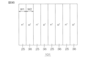
- FIG. 9A is a diagram for explaining channel formation in the semiconductor device 101 according to Condition 1.
- FIG. 9B is a diagram for explaining the arrangement pattern of the emitter region 25 and the contact region 36 of the semiconductor device 101 according to Condition 1.
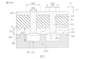
- FIG. 10A is a diagram for explaining channel formation in the semiconductor device 201 according to Condition 2.
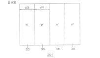
- FIG. 10B is a diagram for explaining the arrangement pattern of the emitter region 25 and the contact region 36 of the semiconductor device 201 according to Condition 2.
- structures corresponding to the semiconductor device 1 are given the same reference numerals and the description thereof will be omitted.
- semiconductor device 101 has the same structure as semiconductor device 1.
- the emitter region 25 is formed deeper than the upper surface of the gate electrode layer 14 in the gate electrode recess 15 (the bottom wall 22 of the gate electrode recess 15). That is, the bottom portion 50 of the emitter region 25 is located in the second main region with respect to the upper surface of the gate electrode layer 14 (bottom wall 22 of the gate electrode recess 15) in the peripheral portions 9 on both sides of the first intersection region 33 in the first direction It is located on the surface 4 side (the opposite side of the first main surface 3).
- the depth D1 of the emitter region 25 from the first main surface 3 is greater than the depth D2 of the gate electrode recess 15 from the first main surface 3 (D1>D2).
- the emitter region 25 has opposing portions 40 that face the gate electrode layer 14 with the gate insulating layer 13 interposed therebetween below the peripheral portion 9 on both sides of the first intersection region 33 in the first direction X. .
- the width W1 of the emitter region 25 in the first direction X is, for example, 1.0 ⁇ m or less, and preferably 0.5 ⁇ m or more and 1.0 ⁇ m or less.
- the width W2 of the contact region 36 in the first direction X may be equal to or slightly wider than the width of the contact trench 31 in the first direction.
- emitter region 25 is formed shallower than the upper surface of gate electrode layer 14 in gate electrode recess 15 (bottom wall 22 of gate electrode recess 15).
- the bottom portion 50 of the emitter region 25 is located in the first main region relative to the upper surface of the gate electrode layer 14 (bottom wall 22 of the gate electrode recess 15) in the peripheral portions 9 on both sides of the first intersection region 33 in the first direction It is located on the surface 3 side.
- the depth D1 of the emitter region 25 from the first main surface 3 is smaller than the depth D2 of the gate electrode recess 15 from the first main surface 3 (D1 ⁇ D2).
- the width W3 of the emitter region 25 in the first direction X exceeds, for example, 1.0 ⁇ m.
- the width W4 of the contact region 36 in the first direction X may be equal to or slightly wider than the width of the contact trench 31 in the first direction.
- the width W5 of the gate electrode recess 15 in the first direction is set wider than the width W6 of the contact trench 31 in the first direction. This is to ensure a margin in consideration of positional deviation during patterning of the mask 78 for forming the contact trench 31 (see FIGS. 8L and 8M).
- the emitter contact electrode layer 51 falls within the range of the gate covering insulating layer 16, and the emitter contact electrode layer 51 is reliably insulated from the gate electrode layer 14 by the gate covering insulating layer 16. This avoids emitter-gate short circuits. That is, it is necessary to make the digging width of the gate electrode layer 14 (the width W5 of the gate electrode recess 15) wider than the contact dimension of the emitter contact electrode layer 51 (the width W6 of the contact trench 31).
- the region of the body region 8 excluding the region below the gate electrode recess 15 is a region in which a main current path can be formed in the channel formation region 202 in which a channel CH can be formed, and
- the region below the electrode recess 15 is a region in which it is difficult to form a main current path.
- the channel width tends to decrease and the on-resistance increases.
- the channel forming region 202 is shown by hatching including solid lines and broken lines.
- the width W3 of the emitter region 25 must be designed to be relatively wide in consideration of the etching margin. This is because if the width W3 of the emitter region 25 is too narrow, the portion of the emitter region 25 facing the gate electrode layer 14 will be significantly reduced after the gate electrode recess 15 is formed.
- the entire region of the body region 8 in the first direction X, including the region below the gate electrode recess 15, is the channel formation region 102 in which a main current path can be formed.
- the channel width can be increased compared to the semiconductor device 201, and the on-resistance can be reduced.
- the channel forming region 102 is shown by hatching including solid lines and broken lines.
- the width W1 of the emitter region 25 there is no need to consider the etching margin and the pattern of the gate electrode recess 15. This is because even after the gate electrode recess 15 is formed, the opposing portion 40 of the emitter region 24 can be secured below the peripheral portion 9, and thereby the channel forming region 102 having a sufficient channel width can be secured. Therefore, the width W1 of the emitter region 25 can be made narrower than the width W3 of the emitter region 25 of the semiconductor device 201.
- FIG. 11 is a graph obtained by simulation of the short circuit waveforms of the semiconductor device 101 according to condition 1 and the semiconductor device 201 according to condition 2.
- the left vertical axis is collector current IC [A]
- the right vertical axis is collector-emitter voltage VCE [V]
- the horizontal axis is time [s].
- the gate voltages under conditions 1 and 2 are shown in a broken line graph
- the collector voltages under conditions 1 and 2 are shown in a solid line graph
- the collector currents under conditions 1 and 2 are shown in a dash-dotted line graph.
- the breakdown resistance can be improved.
- FIG. 12 is a graph obtained by simulation of the current-voltage characteristics of the semiconductor device 101 according to condition 1 and the semiconductor device 201 according to condition 2.
- FIG. 13 is an enlarged view of a part of the graph of FIG. 12.
- the vertical axis is collector current IC [A]
- the horizontal axis is collector-emitter voltage VCE [V].
- FIG. 13 shows a graph in which the collector-emitter voltage VCE of FIG. 12 is in the range of 0 to 2V.
- Condition 1 the characteristics of the semiconductor device 101 according to Condition 1 are shown by a solid line graph, and the characteristics of the semiconductor device 201 according to Condition 2 are shown by a broken line graph. Both Condition 1 and Condition 2 show current-voltage characteristics when the collector-emitter voltage VCE is varied from 0V to 10V.
- the collector-emitter voltages VCE when the collector current IC is 20A, 40A, 60A, 80A, and 100A are 1.26V, 1.60V, and 1.91V, respectively. , 2.25V and 2.66V.
- the collector-emitter voltages VCE when the collector current IC is 20A, 40A, 60A, 80A, and 100A are 1.28V, 1.65V, and 2. .01V, 2.42V and 3.20V.
- the collector-emitter voltage VCE required for startup can be reduced compared to the semiconductor device 201, so that the on-loss can be reduced.
- FIG. 14 is a graph obtained by simulation of the current-voltage characteristics of the semiconductor device 101 according to condition 1 and the semiconductor device 201 according to condition 2.
- the vertical axis is collector current IC [A]
- the horizontal axis is gate-emitter voltage VGE [V].
- the characteristics of the semiconductor device 101 according to Condition 1 are shown by a solid line graph
- the characteristics of the semiconductor device 201 according to Condition 2 are shown by a broken line graph. Both Condition 1 and Condition 2 show current-voltage characteristics when the gate-emitter voltage VGE is changed from 0V to 15V.
- FIG. 15 is a schematic cross-sectional perspective view showing a partial region of a semiconductor device 81 according to a second embodiment of the present disclosure.
- FIG. 16 is a schematic cross-sectional view showing a part of the semiconductor device 81 of FIG. 15.
- FIG. 17 is a schematic cross-sectional view showing a part of the semiconductor device 81 of FIG. 15.
- the gate electrode layer 14 has an uneven structure including a plurality of gate electrode recesses 15.
- the gate electrode layer 14 has a flat structure in which the depth position of the upper surface 82 is constant throughout. More specifically, with reference to FIGS. 16 and 17, the upper surface 82 of the gate electrode layer 14 is located in a region between the first main surface 3 and the bottom 50 of the emitter region 25 with respect to the normal direction Z. ing.
- the emitter region 25 similarly to the semiconductor device 1, the emitter region 25 has a facing portion 40 that faces the gate electrode layer 14 with the gate insulating layer 13 interposed therebetween in the vicinity of the first intersection region 33 in the first direction X. There is.
- the gate covering insulating layer 16 has an integral structure extending across the plurality of contact trenches 31 along the first direction X.
- the gate covering insulating layer 16 has an insulating layer uneven structure formed by insulating layer recesses 83 formed in the first intersection region 33 of each contact trench 31 .
- Emitter contact electrode layer 51 is embedded in insulating layer recess 83 .
- the gate covering insulating layer 16 has a base portion 85 having a flat lower surface 84 in contact with the upper surface 82 of the gate electrode layer 14 along the first direction A convex portion 86 protruding from the portion 85 may be included.
- the uneven structure of the gate covering insulating layer 16 is formed by alternately arranging convex portions 86 and insulating layer concave portions 83 along the first direction X.
- the semiconductor device 81 can also achieve the same effects as those described for the semiconductor device 1.
- the entire region of the body region 8 in the first direction X can be used as the channel formation region 102 in which the channel CH can be formed.
- the semiconductor device 81 when etching the first base conductor layer 74 in the method for manufacturing the semiconductor device 1 (see FIG. 8F), the first base conductor layer 74 is etched without patterning. It can be manufactured by digging almost the entire surface.
- FIG. 18 is a schematic cross-sectional perspective view showing a partial region of a semiconductor device 91 according to a third embodiment of the present disclosure.
- structures corresponding to those described for the semiconductor device 1 will be given the same reference numerals and descriptions will be omitted.
- the semiconductor device 1 described above an example has been described in which the p-type collector region 5 is formed on the surface portion of the second main surface 4.
- an n-type drain region 92 is formed on the surface portion of the second main surface 4 instead of the p-type collector region 5 .
- the semiconductor device 91 has a basic configuration including a trench gate type MISFET (Metal Insulator Semiconductor Field Effect Transistor).
- MISFET Metal Insulator Semiconductor Field Effect Transistor
- the semiconductor device 91 can also achieve the same effects as those described for the semiconductor device 1.
- the semiconductor device 91 can be manufactured by simply forming an n-type drain region 92 in place of the p-type collector region 5 and changing the layout of each mask in the method for manufacturing the semiconductor device 1.
- a structure may be adopted in which the conductivity type of each semiconductor portion is inverted. That is, the p-type portion may be made into the n-type, and the n-type portion may be made into the p-type.
- chip 2 is made of silicon single crystal.
- chip 2 may also include SiC.
- the chip 2 may be made of SiC single crystal.
- the gate trench (12) includes an intersection region (33) that intersects with the gate trench (12), and extends from the intersection region (33) to the gate trench (12) along a second direction (Y) that intersects the first direction (X).
- a spatial region (15) is formed above the gate electrode (14) at least in the crossing region (33) and a peripheral portion (9) of the crossing region (33) in the gate trench (12), The spatial region (15) covers the upper surface (22) of the gate electrode (14) in the intersection region (33) and the periphery (9) of the intersection region (33), and the gate electrode (14) and a covering insulating layer (16) that insulates between the contact electrode (51) and the contact electrode (51),
- the first impurity region (25) is formed deeper than the upper surface (22) of the gate electrode (14) in the peripheral portion (9) of the intersection region (33). , 101).
- the first impurity region (25) has a facing portion (40) facing the gate electrode (14) below the peripheral portion (9) of the crossing region (33).
- the contact electrode (51) is connected to the body region (8) at the bottom wall of the contact trench (31), and connected to the first impurity region (25) at the side wall of the contact trench (31). , the semiconductor device (1, 81, 91, 101) according to Supplementary Note 1-1 or Supplementary Note 1-2.
- the peripheral part (9) of the intersection area (33) includes an area within a range of 0.05 ⁇ m or more and 0.5 ⁇ m or less from the intersection area (33), according to any one of Supplementary notes 1-1 to 1-5. (1, 81, 91, 101).
- the gate electrode (14) is a gate formed in the intersection region (33) of each contact trench (31) and the peripheral portion (9) of the intersection region (33) along the first direction (X). It has an electrode uneven structure formed by an electrode recess (15),
- the semiconductor device (1, 91, 101) according to any one of Supplementary notes 1-1 to 1-6, wherein the covering insulating layer (16) is embedded in the gate electrode recess (15).
- the gate electrode recess (15) is formed across a peripheral portion (9) on one side and a peripheral portion (9) on the other side of the intersection region (33) in the first direction (X),
- the covering insulating layer (16) includes a first portion (47) disposed in the intersection region (33) and a peripheral portion on one side in the first direction (X) with respect to the first portion (47). (9) and a second portion (48) disposed in each of the peripheral portions (9) on the other side (1, 91, 101). ).
- the width (W6) of the contact trench (31) in the first direction (X) is 0.3 ⁇ m or more and 1.0 ⁇ m or less, Side walls of the gate electrode recess (15) are formed on both sides of the contact trench (31) in the first direction (X) with an interval of 0.05 ⁇ m or more and 0.5 ⁇ m or less.
- the semiconductor device (1, 91, 101) according to any one of 1-7 to Supplementary Note 1-9.
- the covering insulating layer (16) has an integral structure extending across the plurality of contact trenches (31) along the first direction (X), and has an integral structure extending across the plurality of contact trenches (31). It has an insulating layer uneven structure formed by insulating layer recesses (83) formed in the region (33), The semiconductor device (81) according to appendix 1-11, wherein the contact electrode (51) is embedded in the insulating layer recess (83).
- the covering insulating layer (16) is adjacent to a base portion (85) having a flat lower surface (84) in contact with the upper surface (82) of the gate electrode (14) along the first direction (X). a convex portion (86) protruding from the base portion (85) between the insulating layer concave portions (83); Supplementary note 1-12, wherein the insulating layer uneven structure is formed by alternately arranging the convex portions (86) and the insulating layer concave portions (83) along the first direction (X).
- the first impurity region (25) includes an emitter region (25), The semiconductor device (1, 81, 101) according to any one of Appendixes 1-1 to 1-13, wherein the contact electrode (51) includes an emitter contact electrode (51).
- the first impurity region (25) includes a source region (25), The semiconductor device (91) according to any one of Appendixes 1-1 to 1-13, wherein the contact electrode (51) includes a source contact electrode (51).
Abstract
Provided is a semiconductor device comprising: a gate electrode layer embedded in a gate trench; a contact trench including a first intersecting region intersecting the gate trench; and an emitter contact electrode layer embedded in the contact trench. A gate electrode recess is formed in the first intersecting region and a peripheral portion to the first intersecting region of the gate trench. A gate-coating insulation layer is embedded in the gate electrode recess. The emitter region is formed deeper than the upper surface of the gate electrode layer in the peripheral portion to the first intersecting region.
Description
本出願は、2022年9月9日に日本国特許庁に提出された特願2022-143916号に対応しており、この出願の全開示はここに引用により組み込まれるものとする。
This application corresponds to Japanese Patent Application No. 2022-143916 filed with the Japan Patent Office on September 9, 2022, and the entire disclosure of this application is hereby incorporated by reference.
本開示は、半導体装置に関する。
The present disclosure relates to a semiconductor device.
特許文献1は、トレンチが形成された主面を有する半導体層と、前記半導体層の前記主面の表面部において前記トレンチの側壁に沿って形成された第1導電型のボディ領域と、前記ボディ領域の表面部において前記トレンチの側壁に沿って形成された第2導電型の不純物領域と、前記トレンチの内壁に形成されたゲート絶縁層と、前記トレンチに埋め込まれ、前記ゲート絶縁層を挟んで前記ボディ領域および前記不純物領域と対向するゲート電極と、前記トレンチ内から前記トレンチの側壁を貫通して前記半導体層の前記主面の表面部に引き出され、前記ボディ領域および前記不純物領域に電気的に接続されたコンタクト電極と、前記トレンチ内において前記ゲート電極および前記コンタクト電極の間に介在し、前記ゲート電極および前記コンタクト電極を絶縁する埋め込み絶縁層とを含む、半導体装置を開示している。
Patent Document 1 discloses a semiconductor layer having a main surface in which a trench is formed, a body region of a first conductivity type formed along a sidewall of the trench in a surface portion of the main surface of the semiconductor layer, and a body region of the body. a second conductivity type impurity region formed along the sidewalls of the trench in the surface portion of the region; a gate insulating layer formed on the inner wall of the trench; and an impurity region buried in the trench and sandwiching the gate insulating layer. A gate electrode facing the body region and the impurity region, and a gate electrode extending from within the trench through the sidewall of the trench to the surface portion of the main surface of the semiconductor layer and electrically connected to the body region and the impurity region. A semiconductor device is disclosed, including a contact electrode connected to the trench, and a buried insulating layer interposed between the gate electrode and the contact electrode in the trench and insulating the gate electrode and the contact electrode.
本開示の一実施形態は、エミッタ領域およびソース領域等の第1不純物領域の寸法の設計自由度を向上でき、それにより破壊耐量を向上することができる半導体装置を提供する。
An embodiment of the present disclosure provides a semiconductor device that can improve the degree of freedom in designing dimensions of first impurity regions such as an emitter region and a source region, thereby improving breakdown resistance.
本開示の一実施形態は、ゲートトレンチに交差するコンタクトトレンチを含む構造において、チャネル幅の縮小を抑制し、オン抵抗を低減することができる半導体装置を提供する。
An embodiment of the present disclosure provides a semiconductor device that can suppress reduction in channel width and reduce on-resistance in a structure including a contact trench that intersects with a gate trench.
本開示の一実施形態に係る半導体装置は、底壁および側壁を有する第1方向に延びるゲートトレンチが形成された第1主面を有するチップと、前記第1主面の表面部において前記ゲートトレンチの前記側壁に沿って形成された第1導電型のボディ領域と、前記ボディ領域の表面部において前記ゲートトレンチの前記側壁に沿って形成された第2導電型の第1不純物領域と、前記ゲートトレンチの前記底壁および前記側壁に形成されたゲート絶縁層と、前記ゲートトレンチに埋め込まれ、前記ゲート絶縁層を挟んで前記ボディ領域および前記第1不純物領域に対向するゲート電極と、前記ゲートトレンチと交差する交差領域を含み、前記第1方向に交差する第2方向に沿って前記交差領域から前記ゲートトレンチの外側に引き出されたコンタクトトレンチと、前記コンタクトトレンチに埋め込まれ、前記コンタクトトレンチの内部で前記ボディ領域および前記第1不純物領域に電気的に接続されたコンタクト電極とを含み、前記ゲートトレンチにおける少なくとも前記交差領域および前記交差領域の周辺部には、前記ゲート電極上に空間領域が形成されており、前記空間領域には、前記交差領域および前記交差領域の周辺部において前記ゲート電極の上面を被覆し、前記ゲート電極と前記コンタクト電極との間を絶縁する被覆絶縁層が埋め込まれており、前記第1不純物領域は、前記交差領域の周辺部における前記ゲート電極の上面よりも深く形成されている。
A semiconductor device according to an embodiment of the present disclosure includes a chip having a first main surface in which a gate trench extending in a first direction having a bottom wall and a side wall is formed, and the gate trench is formed in a surface portion of the first main surface. a body region of a first conductivity type formed along the sidewall of the gate trench; a first impurity region of a second conductivity type formed along the sidewall of the gate trench in a surface portion of the body region; a gate insulating layer formed on the bottom wall and the side wall of the trench, a gate electrode embedded in the gate trench and facing the body region and the first impurity region with the gate insulating layer in between, and the gate trench. a contact trench that includes an intersection region that intersects with the first direction, and is drawn out from the intersection region to the outside of the gate trench along a second direction that intersects with the first direction; a contact electrode electrically connected to the body region and the first impurity region, and a space region is formed on the gate electrode in at least the crossing region and a peripheral portion of the crossing region in the gate trench. A covering insulating layer is embedded in the spatial region to cover the upper surface of the gate electrode in the intersection region and a peripheral portion of the intersection region, and to insulate between the gate electrode and the contact electrode. The first impurity region is formed deeper than the upper surface of the gate electrode in a peripheral portion of the intersection region.
本開示の一実施形態によれば、第1不純物領域は、交差領域の周辺部におけるゲート電極の上面よりも深く形成されている。これにより、交差領域の周辺部においてチャネルを形成できるので、チャネル幅の縮小を抑制し、オン抵抗を低減することができる。
According to an embodiment of the present disclosure, the first impurity region is formed deeper than the upper surface of the gate electrode in the peripheral portion of the intersection region. Thereby, a channel can be formed in the periphery of the intersection region, so that reduction in channel width can be suppressed and on-resistance can be reduced.
本開示の一実施形態によれば、第1不純物領域はゲート電極の上面よりも深く形成されている。これにより、交差領域の周辺部の下部領域にもチャネルが形成可能となる。そのため、エッチングやコンタクトパターン形成時のパターニングのマージンを考慮する必要がなくなり、第1不純物領域の寸法の設計自由度を向上でき、それにより破壊耐量を向上することができる。
According to an embodiment of the present disclosure, the first impurity region is formed deeper than the upper surface of the gate electrode. This allows a channel to be formed also in the lower region around the intersection region. Therefore, there is no need to consider the patterning margin during etching or contact pattern formation, and the degree of freedom in designing the dimensions of the first impurity region can be improved, thereby improving the breakdown resistance.
≪半導体装置1(第1実施形態)の構造の説明≫
図1は、本開示の第1実施形態に係る半導体装置1の一部の領域を示す模式的な断面斜視図である。図2は、図1からチップ2の第1主面3の上の構造を取り除いた図である。図3は、図2からエミッタコンタクト電極層51を取り除いた図である。 <<Description of structure of semiconductor device 1 (first embodiment)>>
FIG. 1 is a schematic cross-sectional perspective view showing a partial region of asemiconductor device 1 according to a first embodiment of the present disclosure. FIG. 2 is a diagram in which the structure on the first main surface 3 of the chip 2 is removed from FIG. 1. FIG. 3 is a diagram from FIG. 2 with the emitter contact electrode layer 51 removed.
図1は、本開示の第1実施形態に係る半導体装置1の一部の領域を示す模式的な断面斜視図である。図2は、図1からチップ2の第1主面3の上の構造を取り除いた図である。図3は、図2からエミッタコンタクト電極層51を取り除いた図である。 <<Description of structure of semiconductor device 1 (first embodiment)>>
FIG. 1 is a schematic cross-sectional perspective view showing a partial region of a
図4は、図3をチップ2の第1主面3から見た模式的な平面図である。図5は、図4に示すV-V線に沿う断面図である。図6は、図4に示すVI-VI線に沿う断面図である。図7は、図4に示すVII-VII線に沿う断面図である。図5~図7では、チップ2の第1主面3の上の構造も図示している。
FIG. 4 is a schematic plan view of FIG. 3 viewed from the first main surface 3 of the chip 2. FIG. 5 is a sectional view taken along the line VV shown in FIG. 4. FIG. 6 is a cross-sectional view taken along line VI-VI shown in FIG. 4. FIG. 7 is a cross-sectional view taken along line VII-VII shown in FIG. 4. 5 to 7 also illustrate the structure on the first main surface 3 of the chip 2.
半導体装置1は、この実施形態では、トレンチゲート型のIGBT(Insulated Gate Bipolar Transistor)を備えた基本形態を有している。図1~図7を参照して、半導体装置1は、n-型のチップ2を含む。チップ2は、この実施形態では、n-型のシリコン単結晶基板からなる。シリコン単結晶基板は、FZ(Floating Zone)法を経て製造されたn-型のシリコン単結晶の半導体ウエハを用いて形成されている。チップ2は、半導体チップと称されてもよいし、半導体層と称されてもよい。
In this embodiment, the semiconductor device 1 has a basic configuration including a trench gate type IGBT (Insulated Gate Bipolar Transistor). Referring to FIGS. 1 to 7, semiconductor device 1 includes an n − type chip 2. Referring to FIGS. In this embodiment, the chip 2 is made of an n - type silicon single crystal substrate. The silicon single crystal substrate is formed using an n − type silicon single crystal semiconductor wafer manufactured through the FZ (Floating Zone) method. The chip 2 may be called a semiconductor chip or a semiconductor layer.
チップ2は、一方側の第1主面3および他方側の第2主面4を有している。チップ2の厚さは、50μm以上300μm以下であってもよい。チップ2の厚さは、50μm以上100μm以下、100μm以上150μm以下、150μm以上200μm以下、200μm以上250μm以下、または、250μm以上300μm以下であってもよい。
The chip 2 has a first main surface 3 on one side and a second main surface 4 on the other side. The thickness of the chip 2 may be 50 μm or more and 300 μm or less. The thickness of the chip 2 may be 50 μm or more and 100 μm or less, 100 μm or more and 150 μm or less, 150 μm or more and 200 μm or less, 200 μm or more and 250 μm or less, or 250 μm or more and 300 μm or less.
第2主面4の表面部には、p型のコレクタ領域5が形成されている。第1主面3の表面部には、n型の電荷蓄積領域6が形成されている。電荷蓄積領域6は、コレクタ領域5に対して第1主面3側に間隔を空けて形成されている。
A p-type collector region 5 is formed on the surface portion of the second main surface 4. An n-type charge storage region 6 is formed in the surface portion of the first main surface 3 . The charge storage region 6 is formed at a distance from the collector region 5 on the first main surface 3 side.
チップ2においてコレクタ領域5および電荷蓄積領域6の間の領域には、n-型のドリフト領域7が形成されている。ドリフト領域7は、チップ2においてコレクタ領域5および電荷蓄積領域6の間に位置する領域によって形成されている。電荷蓄積領域6の表面部には、p型のボディ領域8が形成されている。第1主面3の表面部には、複数のトレンチゲート電極構造10および複数のトレンチエミッタ電極構造11が間隔を空けて形成されている。
In the chip 2, an n − type drift region 7 is formed in a region between the collector region 5 and the charge storage region 6. Drift region 7 is formed by a region located between collector region 5 and charge storage region 6 in chip 2 . A p-type body region 8 is formed on the surface of the charge storage region 6 . A plurality of trench gate electrode structures 10 and a plurality of trench emitter electrode structures 11 are formed at intervals on the surface portion of the first main surface 3.
図1~図7では、互いに隣り合う1つのトレンチゲート電極構造10および1つのトレンチエミッタ電極構造11だけが示されている。以下では、これら1つのトレンチゲート電極構造10および1つのトレンチエミッタ電極構造11の構造に着目して半導体装置1の構造について説明する。
In FIGS. 1 to 7, only one trench gate electrode structure 10 and one trench emitter electrode structure 11 adjacent to each other are shown. The structure of the semiconductor device 1 will be described below, focusing on the structure of one trench gate electrode structure 10 and one trench emitter electrode structure 11.
トレンチゲート電極構造10およびトレンチエミッタ電極構造11は、平面視において、任意の第1方向Xに沿って帯状に延びている。トレンチゲート電極構造10およびトレンチエミッタ電極構造11は、第1方向Xに交差する第2方向Yに沿って間隔を空けて形成されている。
The trench gate electrode structure 10 and the trench emitter electrode structure 11 extend in a band shape along an arbitrary first direction X in plan view. The trench gate electrode structure 10 and the trench emitter electrode structure 11 are formed at intervals along a second direction Y that intersects the first direction X.
平面視とは、より具体的には、第1主面3の法線方向Z(以下、単に「法線方向Z」という。)から見た平面視のことをいう。第2方向Yは、より具体的には、第1方向Xに直交する方向である。第1方向Xおよび第2方向Yは、第1主面3の接線方向でもある。
More specifically, the planar view refers to a planar view seen from the normal direction Z of the first principal surface 3 (hereinafter simply referred to as "normal direction Z"). More specifically, the second direction Y is a direction perpendicular to the first direction X. The first direction X and the second direction Y are also tangential directions of the first main surface 3.
トレンチゲート電極構造10およびトレンチエミッタ電極構造11の間のトレンチピッチP0は、0.1μm以上0.6μm未満であってもよい。トレンチピッチP0は、0.1μm以上0.2μm以下、0.2μm以上0.3μm以下、0.3μm以上0.4μm以下、0.4μm以上0.5μm以下、または、0.5μm以上0.6μm未満であってもよい。トレンチピッチP0は、0.2μm以上0.4μm以下(たとえば0.25μm程度)であることが好ましい。
The trench pitch P0 between the trench gate electrode structure 10 and the trench emitter electrode structure 11 may be 0.1 μm or more and less than 0.6 μm. Trench pitch P0 is 0.1 μm or more and 0.2 μm or less, 0.2 μm or more and 0.3 μm or less, 0.3 μm or more and 0.4 μm or less, 0.4 μm or more and 0.5 μm or less, or 0.5 μm or more and 0.6 μm It may be less than The trench pitch P0 is preferably 0.2 μm or more and 0.4 μm or less (for example, about 0.25 μm).
トレンチゲート電極構造10は、ゲートトレンチ12、ゲート絶縁層13、ゲート電極層14、複数のゲート電極凹部15(空間領域)および複数のゲート被覆絶縁層16を含む。ゲートトレンチ12は、第1主面3からボディ領域8および電荷蓄積領域6を貫通してドリフト領域7に至る。
The trench gate electrode structure 10 includes a gate trench 12 , a gate insulating layer 13 , a gate electrode layer 14 , a plurality of gate electrode recesses 15 (space regions), and a plurality of gate covering insulating layers 16 . Gate trench 12 extends from first main surface 3 through body region 8 and charge storage region 6 to drift region 7 .
ゲートトレンチ12の深さは、2.0μm以上4.0μm以下であってもよい。ゲートトレンチ12の深さは、2.0μm以上2.5μm以下、2.5μm以上3.0μm以下、3.0μm以上3.5μm以下、または、3.5μm以上4.0μm以下であってもよい。ゲートトレンチ12の深さは、2.5μm以上3.5μm以下(たとえば3.0μm程度)であることが好ましい。
The depth of the gate trench 12 may be 2.0 μm or more and 4.0 μm or less. The depth of the gate trench 12 may be 2.0 μm or more and 2.5 μm or less, 2.5 μm or more and 3.0 μm or less, 3.0 μm or more and 3.5 μm or less, or 3.5 μm or more and 4.0 μm or less. . The depth of the gate trench 12 is preferably 2.5 μm or more and 3.5 μm or less (for example, about 3.0 μm).
ゲートトレンチ12の第2方向幅は、0.5μm以上1.5μm以下であってもよい。ゲートトレンチ12の第2方向幅は、0.5μm以上0.75μm以下、0.75μm以上1.0μm以下、1.0μm以上1.25μm以下、または、1.25μm以上1.5μm以下であってもよい。ゲートトレンチ12の第2方向幅は、0.5μm以上1.0μm以下(たとえば0.75μm程度)であることが好ましい。
The width of the gate trench 12 in the second direction may be 0.5 μm or more and 1.5 μm or less. The width of the gate trench 12 in the second direction is 0.5 μm or more and 0.75 μm or less, 0.75 μm or more and 1.0 μm or less, 1.0 μm or more and 1.25 μm or less, or 1.25 μm or more and 1.5 μm or less. Good too. The width of the gate trench 12 in the second direction is preferably 0.5 μm or more and 1.0 μm or less (for example, about 0.75 μm).
ゲート絶縁層13は、酸化シリコンにより形成されていてもよい。ゲート絶縁層13は、ゲートトレンチ12の内壁に沿って膜状に形成されている。ゲート絶縁層13は、ゲートトレンチ12内において凹状の空間を区画している。
The gate insulating layer 13 may be formed of silicon oxide. The gate insulating layer 13 is formed in a film shape along the inner wall of the gate trench 12 . Gate insulating layer 13 defines a concave space within gate trench 12 .
ゲート電極層14は、導電性のポリシリコンにより形成されていてもよい。ゲート電極層14は、ゲート電圧によって制御される。ゲート電極層14は、ゲート絶縁層13を挟んでゲートトレンチ12に埋め込まれている。ゲート電極層14は、より具体的には、ゲートトレンチ12内においてゲート絶縁層13によって区画された凹状の空間に埋め込まれている。ゲート電極層14の上端部は、ボディ領域8の底部に対して第1主面3側に位置している。
The gate electrode layer 14 may be formed of conductive polysilicon. Gate electrode layer 14 is controlled by gate voltage. The gate electrode layer 14 is embedded in the gate trench 12 with the gate insulating layer 13 in between. More specifically, the gate electrode layer 14 is embedded in a concave space defined by the gate insulating layer 13 within the gate trench 12 . The upper end of the gate electrode layer 14 is located on the first main surface 3 side with respect to the bottom of the body region 8 .
複数のゲート電極凹部15は、この実施形態では、第1方向Xに沿って間隔を空けてゲート電極層14の主面に形成されている。これにより、ゲート電極層14の上端部は、複数のゲート電極凹部15を含む凹凸構造を有している。
In this embodiment, the plurality of gate electrode recesses 15 are formed on the main surface of the gate electrode layer 14 at intervals along the first direction X. As a result, the upper end portion of the gate electrode layer 14 has an uneven structure including a plurality of gate electrode recesses 15.
互いに隣り合う複数のゲート電極凹部15の間隔は、0μmを超えて10μm以下であってもよい。互いに隣り合う複数のゲート電極凹部15の間隔は、ゲート電極層14において互いに隣り合う2つのゲート電極凹部15によって挟まれた部分の第1方向Xの幅でもある。互いに隣り合う複数のゲート電極凹部15の間隔は、0μmを超えて2μm以下、2μm以上4μm以下、4μm以上6μm以下、6μm以上8μm以下、または、8μm以上10μm以下であってもよい。
The interval between the plurality of gate electrode recesses 15 adjacent to each other may be greater than 0 μm and less than or equal to 10 μm. The interval between the plurality of gate electrode recesses 15 adjacent to each other is also the width in the first direction X of a portion of the gate electrode layer 14 sandwiched between two gate electrode recesses 15 adjacent to each other. The interval between the plurality of gate electrode recesses 15 adjacent to each other may be more than 0 μm and less than 2 μm, more than 2 μm and less than 4 μm, more than 4 μm and less than 6 μm, more than 6 μm and less than 8 μm, or more than 8 μm and less than 10 μm.
各ゲート電極凹部15の側壁は、この実施形態では、ゲート絶縁層13およびゲート電極層14により形成されている。各ゲート電極凹部15の底壁22は、ゲート電極層14により形成されている。図6および図7を参照して、各ゲート電極凹部15の底壁22は、法線方向Zに関して、第1主面3およびエミッタ領域25(後述)の底部50の間の領域に位置している。
In this embodiment, the side walls of each gate electrode recess 15 are formed by the gate insulating layer 13 and the gate electrode layer 14. The bottom wall 22 of each gate electrode recess 15 is formed of the gate electrode layer 14. Referring to FIGS. 6 and 7, the bottom wall 22 of each gate electrode recess 15 is located in a region between the first main surface 3 and the bottom 50 of the emitter region 25 (described later) with respect to the normal direction Z. There is.
図6を参照して、各ゲート電極凹部15は、底面積が開口面積よりも小さいテーパ形状に形成されている。ゲート電極層14の主面およびゲート電極凹部15の側壁がゲート電極層14内において成す角度θは、90°を超えて105°以下(たとえば102°程度)であってもよい。
Referring to FIG. 6, each gate electrode recess 15 is formed in a tapered shape with a bottom area smaller than the opening area. The angle θ formed by the main surface of the gate electrode layer 14 and the side wall of the gate electrode recess 15 within the gate electrode layer 14 may be more than 90° and less than or equal to 105° (for example, about 102°).
複数のゲート被覆絶縁層16は、ゲートトレンチ12内においてゲート電極層14の上端部にそれぞれ埋め込まれている。ゲート被覆絶縁層16は、より具体的には、ゲート電極凹部15ごとに独立して埋め込まれている。各ゲート被覆絶縁層16は、ゲートトレンチ12の開口から露出している。
The plurality of gate covering insulating layers 16 are each embedded in the upper end portion of the gate electrode layer 14 within the gate trench 12. More specifically, the gate covering insulating layer 16 is embedded independently in each gate electrode recess 15. Each gate covering insulating layer 16 is exposed through the opening of the gate trench 12.
トレンチエミッタ電極構造11は、エミッタトレンチ17、エミッタ絶縁層18、エミッタ電極層19、エミッタ電極凹部20およびエミッタ被覆絶縁層21を含む。エミッタトレンチ17は、第1主面3からボディ領域8および電荷蓄積領域6を貫通してドリフト領域7に至る。
The trench emitter electrode structure 11 includes an emitter trench 17, an emitter insulating layer 18, an emitter electrode layer 19, an emitter electrode recess 20, and an emitter covering insulating layer 21. Emitter trench 17 extends from first main surface 3 through body region 8 and charge storage region 6 to drift region 7 .
エミッタトレンチ17の深さは、2.0μm以上4.0μm以下であってもよい。エミッタトレンチ17の深さは、2.0μm以上2.5μm以下、2.5μm以上3.0μm以下、3.0μm以上3.5μm以下、または、3.5μm以上4.0μm以下であってもよい。エミッタトレンチ17の深さは、2.5μm以上3.5μm以下(たとえば3.0μm程度)であることが好ましい。エミッタトレンチ17の深さは、ゲートトレンチ12の深さとほぼ等しいことが好ましい。
The depth of the emitter trench 17 may be 2.0 μm or more and 4.0 μm or less. The depth of the emitter trench 17 may be 2.0 μm or more and 2.5 μm or less, 2.5 μm or more and 3.0 μm or less, 3.0 μm or more and 3.5 μm or less, or 3.5 μm or more and 4.0 μm or less. . The depth of the emitter trench 17 is preferably 2.5 μm or more and 3.5 μm or less (for example, about 3.0 μm). Preferably, the depth of emitter trench 17 is approximately equal to the depth of gate trench 12.
エミッタトレンチ17の第2方向幅は、0.5μm以上1.5μm以下であってもよい。エミッタトレンチ17の第2方向幅は、0.5μm以上0.75μm以下、0.75μm以上1.0μm以下、1.0μm以上1.25μm以下、または、1.25μm以上1.5μm以下であってもよい。エミッタトレンチ17の第2方向幅は、0.5μm以上1.0μm以下(たとえば0.75μm程度)であることが好ましい。エミッタトレンチ17の第2方向幅は、ゲートトレンチ12の第2方向幅とほぼ等しいことが好ましい。
The width of the emitter trench 17 in the second direction may be 0.5 μm or more and 1.5 μm or less. The width in the second direction of the emitter trench 17 is 0.5 μm or more and 0.75 μm or less, 0.75 μm or more and 1.0 μm or less, 1.0 μm or more and 1.25 μm or less, or 1.25 μm or more and 1.5 μm or less. Good too. The width of the emitter trench 17 in the second direction is preferably 0.5 μm or more and 1.0 μm or less (for example, about 0.75 μm). The width of the emitter trench 17 in the second direction is preferably approximately equal to the width of the gate trench 12 in the second direction.
エミッタ絶縁層18は、酸化シリコンにより形成されていてもよい。エミッタ絶縁層18は、エミッタトレンチ17の内壁面に沿って膜状に形成されている。エミッタ絶縁層18は、エミッタトレンチ17内において凹状の空間を区画している。
The emitter insulating layer 18 may be formed of silicon oxide. Emitter insulating layer 18 is formed in a film shape along the inner wall surface of emitter trench 17 . Emitter insulating layer 18 defines a concave space within emitter trench 17 .
エミッタ電極層19は、導電性のポリシリコンにより形成されていてもよい。エミッタ電極層19は、エミッタ電圧によって制御される。エミッタ電圧は、ゲート電圧未満の電圧値を有している。エミッタ電圧は、基準電圧(たとえばグランド電圧)であってもよい。エミッタ電極層19は、エミッタ絶縁層18を挟んでエミッタトレンチ17に埋め込まれている。エミッタ電極層19は、より具体的には、エミッタトレンチ17内においてエミッタ絶縁層18によって区画された凹状の空間に埋め込まれている。
The emitter electrode layer 19 may be formed of conductive polysilicon. Emitter electrode layer 19 is controlled by emitter voltage. The emitter voltage has a voltage value less than the gate voltage. The emitter voltage may be a reference voltage (eg, ground voltage). Emitter electrode layer 19 is embedded in emitter trench 17 with emitter insulating layer 18 in between. More specifically, the emitter electrode layer 19 is embedded in a concave space defined by the emitter insulating layer 18 in the emitter trench 17 .
エミッタ電極凹部20は、この実施形態では、エミッタ電極層19の主面のほぼ全面を掘り下げるように形成されている。換言すると、エミッタ電極層19は、エミッタ絶縁層18によって区画された凹状の空間の深さ方向途中部まで埋め込まれている。
In this embodiment, the emitter electrode recess 20 is formed so as to dig down almost the entire main surface of the emitter electrode layer 19. In other words, the emitter electrode layer 19 is buried halfway in the depth direction of the concave space defined by the emitter insulating layer 18 .
エミッタ電極凹部20の側壁は、この実施形態では、エミッタ絶縁層18により形成されている。エミッタ電極凹部20の底壁は、エミッタ電極層19により形成されている。エミッタ電極凹部20の底壁は、法線方向Zに関して、第1主面3およびエミッタ領域25(後述)の底部50の間の領域に位置している。つまり、エミッタ電極層19の上端部は、エミッタ領域25の底部50に対して第1主面3側に位置している。法線方向Zに関して、エミッタ電極凹部20の深さは、ゲート電極凹部15の深さにほぼ等しくてもよい。
The side walls of the emitter electrode recess 20 are formed by the emitter insulating layer 18 in this embodiment. The bottom wall of the emitter electrode recess 20 is formed by the emitter electrode layer 19. The bottom wall of the emitter electrode recess 20 is located in a region between the first main surface 3 and the bottom 50 of the emitter region 25 (described later) with respect to the normal direction Z. That is, the upper end of the emitter electrode layer 19 is located on the first main surface 3 side with respect to the bottom 50 of the emitter region 25. With respect to the normal direction Z, the depth of the emitter electrode recess 20 may be approximately equal to the depth of the gate electrode recess 15.
エミッタ被覆絶縁層21は、エミッタトレンチ17内においてエミッタ電極層19の上面に埋め込まれている。エミッタ被覆絶縁層21は、より具体的には、エミッタ電極凹部20に埋め込まれている。これにより、エミッタ被覆絶縁層21は、エミッタ電極層19を封止している。エミッタ被覆絶縁層21は、エミッタトレンチ17の開口から露出している。
The emitter covering insulating layer 21 is embedded in the upper surface of the emitter electrode layer 19 within the emitter trench 17. More specifically, the emitter covering insulating layer 21 is embedded in the emitter electrode recess 20. Thereby, the emitter covering insulating layer 21 seals the emitter electrode layer 19. Emitter covering insulating layer 21 is exposed through the opening of emitter trench 17 .
ボディ領域8の表面部においてゲートトレンチ12の側壁に沿う領域には、n+型のエミッタ領域25(第1不純物領域)が形成されている。エミッタ領域25は、より具体的には、第1方向Xに関して、ゲートトレンチ12の一方側の側壁および他方側の側壁に沿って複数形成されている。複数のエミッタ領域25は、第1方向Xに沿って延びる帯状にそれぞれ形成されている。エミッタ領域25は、ゲートトレンチ12の側壁に接している。エミッタ領域25は、エミッタトレンチ17の側壁にも接している。
An n + type emitter region 25 (first impurity region) is formed in a region along the sidewall of the gate trench 12 in the surface portion of the body region 8 . More specifically, a plurality of emitter regions 25 are formed along one sidewall and the other sidewall of the gate trench 12 in the first direction X. The plurality of emitter regions 25 are each formed in a band shape extending along the first direction X. Emitter region 25 is in contact with the sidewall of gate trench 12 . Emitter region 25 is also in contact with the sidewall of emitter trench 17 .
第1主面3の表面部においてゲートトレンチ12の側壁に沿う領域には、第1主面3から第2主面4側に向けて、エミッタ領域25、ボディ領域8、電荷蓄積領域6およびドリフト領域7がこの順に形成されている。ボディ領域8においてゲート絶縁層13を挟んでゲート電極層14と対向する領域にIGBTのチャネルCHが形成される。
In the region along the sidewall of the gate trench 12 in the surface portion of the first main surface 3, from the first main surface 3 toward the second main surface 4 side, there is an emitter region 25, a body region 8, a charge storage region 6, and a drift region. Regions 7 are formed in this order. An IGBT channel CH is formed in the body region 8 in a region facing the gate electrode layer 14 with the gate insulating layer 13 in between.
図3、図4、図6および図7を参照して、第1主面3の表面部には、複数のコンタクトトレンチ31が形成されている。複数のコンタクトトレンチ31は、第1方向Xに沿って間隔を空けて形成されている。複数のコンタクトトレンチ31は、第2方向Yに沿って延びる帯状にそれぞれ形成されている。各コンタクトトレンチ31の第1方向幅は、ゲートトレンチ12の第2方向幅よりも小さい。各コンタクトトレンチ31の第1方向幅は、たとえば、0.3μm以上1.0μm以下であってもよい。
Referring to FIGS. 3, 4, 6, and 7, a plurality of contact trenches 31 are formed in the surface portion of the first main surface 3. The plurality of contact trenches 31 are formed at intervals along the first direction X. The plurality of contact trenches 31 are each formed in a band shape extending along the second direction Y. The width of each contact trench 31 in the first direction is smaller than the width of the gate trench 12 in the second direction. The width of each contact trench 31 in the first direction may be, for example, 0.3 μm or more and 1.0 μm or less.
各コンタクトトレンチ31は、より具体的には、対応するゲート被覆絶縁層16の内方領域からゲートトレンチ12の側壁を貫通して第1主面3の表面部に引き出されている。各コンタクトトレンチ31は、この実施形態では、第1方向Xに関して、ゲート被覆絶縁層16の内方領域からゲートトレンチ12の一方側の側壁および他方側の側壁を貫通している。各コンタクトトレンチ31の第1方向幅は、対応するゲート被覆絶縁層16の第1方向幅よりも小さい。
More specifically, each contact trench 31 extends from the inner region of the corresponding gate covering insulating layer 16 through the side wall of the gate trench 12 to the surface portion of the first main surface 3. In this embodiment, each contact trench 31 penetrates from the inner region of the gate covering insulating layer 16 to one side wall and the other side wall of the gate trench 12 in the first direction X. The width of each contact trench 31 in the first direction is smaller than the width of the corresponding gate covering insulating layer 16 in the first direction.
各コンタクトトレンチ31は、平面視においてゲート電極層14と交差する第1交差領域33を含む。第1交差領域33において、各コンタクトトレンチ31の側壁および底壁は、ゲート被覆絶縁層16により形成されている。
Each contact trench 31 includes a first intersection region 33 that intersects with the gate electrode layer 14 in plan view. In the first intersection region 33 , the side walls and bottom walls of each contact trench 31 are formed by the gate covering insulating layer 16 .
各コンタクトトレンチ31は、平面視においてエミッタ電極層19と交差する第2交差領域34を含む。第2交差領域34において、各コンタクトトレンチ31の側壁および底壁は、エミッタ被覆絶縁層21により形成されている。
Each contact trench 31 includes a second intersection region 34 that intersects with the emitter electrode layer 19 in plan view. In the second intersection region 34 , the sidewall and bottom wall of each contact trench 31 are formed by the emitter covering insulating layer 21 .
各コンタクトトレンチ31は、第1交差領域33からゲートトレンチ12の外側に引き出されたコンタクト領域35をさらに含む。コンタクト領域35は、平面視においてゲートトレンチ12およびエミッタトレンチ17の間の領域において第1交差領域33および第2交差領域34を接続する接続領域と称されてもよい。コンタクト領域35において、各コンタクトトレンチ31の底壁は、ボディ領域8により形成され、各コンタクトトレンチ31の側壁は、エミッタ領域25により形成されている。つまり、コンタクト領域35においてコンタクトトレンチ31の側壁には、エミッタ領域25が露出している。
Each contact trench 31 further includes a contact region 35 drawn out from the first intersection region 33 to the outside of the gate trench 12 . Contact region 35 may be referred to as a connection region that connects first intersection region 33 and second intersection region 34 in a region between gate trench 12 and emitter trench 17 in plan view. In the contact region 35 , the bottom wall of each contact trench 31 is formed by the body region 8 , and the side wall of each contact trench 31 is formed by the emitter region 25 . That is, the emitter region 25 is exposed on the sidewall of the contact trench 31 in the contact region 35 .
各コンタクトトレンチ31は、さらに、エミッタトレンチ17の一方側の側壁から外側に引き出された引き出し部32を有している。各引き出し部32は、第1主面3の表面部からエミッタトレンチ17の一方側の側壁を貫通し、エミッタトレンチ17内に至る。
Each contact trench 31 further has a drawn-out portion 32 drawn out from one side wall of the emitter trench 17. Each lead-out portion 32 penetrates from the surface portion of the first main surface 3 through one side wall of the emitter trench 17 and reaches into the emitter trench 17 .
各コンタクトトレンチ31の側壁は、第1交差領域33、第2交差領域34およびコンタクト領域35において面一に形成されている。各コンタクトトレンチ31の底壁は、第1交差領域33、第2交差領域34およびコンタクト領域35において面一に形成されている。
The sidewalls of each contact trench 31 are formed flush with each other in the first intersection region 33 , second intersection region 34 , and contact region 35 . The bottom wall of each contact trench 31 is formed flush with the first intersection region 33 , second intersection region 34 , and contact region 35 .
第1交差領域33においてゲート電極層14の上端部は、エミッタ領域25の底部50に対して第1主面3側に位置している。これにより、図6および図7を参照して、エミッタ領域25は、第1方向Xにおける第1交差領域33の両側の周辺部9の下方において、ゲート絶縁層13を介してゲート電極層14に対向する対向部40を有している。
In the first intersection region 33 , the upper end of the gate electrode layer 14 is located on the first main surface 3 side with respect to the bottom 50 of the emitter region 25 . 6 and 7, the emitter region 25 is connected to the gate electrode layer 14 via the gate insulating layer 13 below the peripheral portion 9 on both sides of the first intersection region 33 in the first direction X. It has facing portions 40 that face each other.
ゲート電極層14は、第1方向Xに沿って各コンタクトトレンチ31の第1交差領域33および周辺部9に形成されたゲート電極凹部15によって形成された電極凹凸構造を有している。ゲート電極層14の上面の一部(電極凹凸構造の凸部の上面23)は、隣り合うコンタクトトレンチ31の間において露出している。
The gate electrode layer 14 has an electrode uneven structure formed by the gate electrode recesses 15 formed in the first intersection region 33 of each contact trench 31 and the peripheral portion 9 along the first direction X. A portion of the upper surface of the gate electrode layer 14 (the upper surface 23 of the convex portion of the electrode uneven structure) is exposed between adjacent contact trenches 31 .
ゲート電極凹部15は、第1方向Xにおける第1交差領域33の一方側の周辺部9および他方側の周辺部9に跨って形成されている。これにより、図6および図7を参照して、ゲート被覆絶縁層16は、第1交差領域33に配置された第1部分47と、第1部分47に対して第1方向Xの一方側の周辺部9および他方側の周辺部9それぞれに配置された第2部分48とを有している。
The gate electrode recess 15 is formed across the peripheral portion 9 on one side and the peripheral portion 9 on the other side of the first intersection region 33 in the first direction X. Accordingly, with reference to FIGS. 6 and 7, the gate covering insulating layer 16 has a first portion 47 disposed in the first intersection region 33 and a portion on one side of the first portion 47 in the first direction X. It has a peripheral portion 9 and a second portion 48 disposed in each of the peripheral portion 9 on the other side.
第1交差領域33の周辺部9は、たとえば、コンタクトトレンチ31の側壁からゲート電極凹部15の側壁までの領域であってもよい。周辺部9は、たとえば、第1交差領域33の側壁から0.05μm以上0.5μm以下の範囲の領域であってもよい。つまり、この実施形態では、ゲート電極凹部15の側壁は、第1方向Xにおけるコンタクトトレンチ31の両側のそれぞれに、0.05μm以上0.5μm以下の間隔を空けて形成されている。
The peripheral portion 9 of the first intersection region 33 may be, for example, a region from the side wall of the contact trench 31 to the side wall of the gate electrode recess 15. The peripheral portion 9 may be, for example, a region within a range of 0.05 μm or more and 0.5 μm or less from the side wall of the first intersection region 33. That is, in this embodiment, the side walls of the gate electrode recess 15 are formed on both sides of the contact trench 31 in the first direction X with an interval of 0.05 μm or more and 0.5 μm or less.
複数のコンタクトトレンチ31の配置は、任意である。複数のコンタクトトレンチ31は、第1方向Xに沿って等間隔に形成されていてもよい。複数のコンタクトトレンチ31は、第1方向Xに沿って不等間隔に形成されていてもよい。
The arrangement of the plurality of contact trenches 31 is arbitrary. The plurality of contact trenches 31 may be formed at equal intervals along the first direction X. The plurality of contact trenches 31 may be formed at unequal intervals along the first direction X.
ボディ領域8において各コンタクトトレンチ31の底壁に沿う領域には、p+型のコンタクト領域36が形成されている。コンタクト領域36は、ボディ領域8において各コンタクトトレンチ31の底壁および側壁に沿う領域に形成されていてもよい。
A p + type contact region 36 is formed in a region along the bottom wall of each contact trench 31 in the body region 8 . Contact region 36 may be formed in a region along the bottom wall and side wall of each contact trench 31 in body region 8 .
コンタクト領域36は、コンタクトトレンチ31の底壁から露出した露出面を有している。コンタクト領域36の露出面は、第1主面3およびボディ領域8の底部の間の領域に形成されている。コンタクト領域36の露出面は、より具体的には、第1主面3およびエミッタ領域25の底部50の間の領域に形成されている。この実施形態では、ボディ領域8は、コンタクトトレンチ31に沿って第1主面3側に選択的に突出したボディ領域凸部49を有している。コンタクト領域36は、ボディ領域凸部49の先端部に形成されている。ボディ領域凸部49は、第1方向Xにおいてエミッタ領域25に挟まれている。
The contact region 36 has an exposed surface exposed from the bottom wall of the contact trench 31. The exposed surface of the contact region 36 is formed in a region between the first main surface 3 and the bottom of the body region 8 . More specifically, the exposed surface of the contact region 36 is formed in a region between the first main surface 3 and the bottom 50 of the emitter region 25. In this embodiment, the body region 8 has a body region convex portion 49 that selectively projects toward the first main surface 3 side along the contact trench 31 . The contact region 36 is formed at the tip of the body region convex portion 49 . The body region convex portion 49 is sandwiched between the emitter regions 25 in the first direction X.
図1~図3では、コンタクト領域36が、1回のイオン注入によってコンタクトトレンチ31の底面に浅く形成された例が示されている。しかし、コンタクト領域36は、イオン注入の回数やイオン注入のエネルギを調整することにより、より深く形成されてもよい。たとえば、コンタクト領域36は、エミッタ領域25の底部50よりも深く形成されてもよい。
1 to 3 show an example in which the contact region 36 is formed shallowly on the bottom surface of the contact trench 31 by one-time ion implantation. However, the contact region 36 may be formed deeper by adjusting the number of ion implantations and the energy of ion implantation. For example, contact region 36 may be formed deeper than bottom 50 of emitter region 25.
第1主面3の上には、層間絶縁層41が形成されている。層間絶縁層41は、トレンチゲート電極構造10およびトレンチエミッタ電極構造11を被覆している。層間絶縁層41は、ゲートトレンチ12から露出するゲート被覆絶縁層16、およびエミッタトレンチ17から露出するエミッタ被覆絶縁層21を被覆している。
An interlayer insulating layer 41 is formed on the first main surface 3. Interlayer insulating layer 41 covers trench gate electrode structure 10 and trench emitter electrode structure 11 . The interlayer insulating layer 41 covers the gate covering insulating layer 16 exposed from the gate trench 12 and the emitter covering insulating layer 21 exposed from the emitter trench 17.
層間絶縁層41は、酸化シリコンまたは窒化シリコンにより形成されていてもよい。層間絶縁層41は、酸化膜(SiO2膜)および窒化膜(SiN膜)を含む積層構造を有していてもよい。酸化膜(SiO2膜)は、不純物を含有しないNSG(Nondoped Silicon Glass)膜、および/または、リンを含有するPSG(Phosphorus Silicon Glass)膜を含んでいてもよい。
Interlayer insulating layer 41 may be formed of silicon oxide or silicon nitride. The interlayer insulating layer 41 may have a laminated structure including an oxide film (SiO 2 film) and a nitride film (SiN film). The oxide film (SiO 2 film) may include an NSG (Nondoped Silicon Glass) film that does not contain impurities and/or a PSG (Phosphorus Silicon Glass) film that contains phosphorus.
層間絶縁層41は、第1主面3からこの順に積層されたNSG膜およびPSG膜を含む積層構造を有していてもよい。NSG膜の厚さは、2000Å以上8000Å以下(たとえば5000Å程度)であってもよい。PSG膜の厚さ、2000Å以上6000Å以下(たとえば4000Å程度)であってもよい。
The interlayer insulating layer 41 may have a stacked structure including an NSG film and a PSG film stacked in this order from the first main surface 3. The thickness of the NSG film may be greater than or equal to 2000 Å and less than or equal to 8000 Å (for example, approximately 5000 Å). The thickness of the PSG film may be greater than or equal to 2000 Å and less than or equal to 6000 Å (for example, approximately 4000 Å).
層間絶縁層41には、複数のコンタクト孔42が形成されている。複数のコンタクト孔42は、対応するコンタクトトレンチ31にそれぞれ連通している。つまり、複数のコンタクト孔42は、第1方向Xに沿って間隔を空けて形成され、第2方向Yに沿って延びる帯状にそれぞれ形成されている。
A plurality of contact holes 42 are formed in the interlayer insulating layer 41. Each of the plurality of contact holes 42 communicates with the corresponding contact trench 31 . That is, the plurality of contact holes 42 are formed at intervals along the first direction X, and are each formed in a band shape extending along the second direction Y.
複数のコンタクト孔42は、層間絶縁層41を貫通し、対応するコンタクトトレンチ31にそれぞれ連通している。これにより、複数のコンタクト孔42は、対応するコンタクトトレンチ31との間で一つのエミッタコンタクトトレンチ31,42を形成している。
The plurality of contact holes 42 penetrate the interlayer insulating layer 41 and communicate with the corresponding contact trenches 31, respectively. Thereby, the plurality of contact holes 42 form one emitter contact trench 31, 42 with the corresponding contact trench 31.
各コンタクト孔42の第1方向幅は、各コンタクトトレンチ31の第1方向幅以上であってもよい。つまり、各コンタクト孔42の第1方向幅は、各コンタクトトレンチ31の第1方向幅と等しくてもよいし、各コンタクトトレンチ31の第1方向幅を超えていてもよい。各コンタクト孔42の第1方向幅が各コンタクトトレンチ31の第1方向幅を超えている場合、各コンタクト孔42の内壁は、対応するコンタクトトレンチ31の内壁を取り囲んでいてもよい。
The width of each contact hole 42 in the first direction may be greater than or equal to the width of each contact trench 31 in the first direction. That is, the width of each contact hole 42 in the first direction may be equal to the width of each contact trench 31 in the first direction, or may exceed the width of each contact trench 31 in the first direction. When the width of each contact hole 42 in the first direction exceeds the width of each contact trench 31 in the first direction, the inner wall of each contact hole 42 may surround the inner wall of the corresponding contact trench 31.
複数のコンタクト孔42の配置は、任意であり、コンタクトトレンチ31の配置に応じて調整される。複数のコンタクト孔42は、第1方向X沿って等間隔に形成されていてもよい。複数のコンタクト孔42は、第1方向Xに沿って不等間隔に形成されていてもよい。
The arrangement of the plurality of contact holes 42 is arbitrary and adjusted according to the arrangement of the contact trenches 31. The plurality of contact holes 42 may be formed at equal intervals along the first direction X. The plurality of contact holes 42 may be formed at unequal intervals along the first direction X.
層間絶縁層41の上には、エミッタ主面電極層43が形成されている。エミッタ主面電極層43は、層間絶縁層41の上からコンタクト孔42およびコンタクトトレンチ31(つまり、エミッタコンタクトトレンチ31,42)に入り込んでいる。エミッタ主面電極層43は、たとえば、チタン等のバリア層と、タングステン等の電極層との積層構造を含んでいてもよい。この実施形態では、エミッタ主面電極層43において複数のコンタクトトレンチ31内に位置する部分によって、複数のエミッタコンタクト電極層51が形成されている。これにより、複数のエミッタコンタクト電極層51が、チップ2の表面部に埋め込まれた構造が形成されている。
An emitter main surface electrode layer 43 is formed on the interlayer insulating layer 41. Emitter main surface electrode layer 43 enters contact hole 42 and contact trench 31 (that is, emitter contact trenches 31 and 42) from above interlayer insulating layer 41. The emitter main surface electrode layer 43 may include, for example, a laminated structure of a barrier layer made of titanium or the like and an electrode layer made of tungsten or the like. In this embodiment, a plurality of emitter contact electrode layers 51 are formed by portions of the emitter main surface electrode layer 43 located within the plurality of contact trenches 31 . As a result, a structure in which a plurality of emitter contact electrode layers 51 are embedded in the surface portion of the chip 2 is formed.
複数のエミッタコンタクト電極層51は、複数のコンタクトトレンチ31の配列および形状に対応した配列および形状をそれぞれ有している。つまり、複数のエミッタコンタクト電極層51は、第1方向Xに沿って間隔を空けて形成され、第2方向Yに沿って延びる帯状にそれぞれ形成されている。
The plurality of emitter contact electrode layers 51 each have an arrangement and shape corresponding to the arrangement and shape of the plurality of contact trenches 31. That is, the plurality of emitter contact electrode layers 51 are formed at intervals along the first direction X, and are each formed in a band shape extending along the second direction Y.
各エミッタコンタクト電極層51は、平面視においてゲート電極層14と交差する第1交差領域33において、法線方向Zおよび第1方向Xに関して、ゲート被覆絶縁層16を挟んでゲート電極層14と対向している。各エミッタコンタクト電極層51は、ゲート被覆絶縁層16によってゲート電極層14から絶縁されている。各エミッタコンタクト電極層51の第1方向幅は、ゲートトレンチ12の第1方向幅よりも小さい。
Each emitter contact electrode layer 51 faces the gate electrode layer 14 with the gate covering insulating layer 16 in between with respect to the normal direction Z and the first direction are doing. Each emitter contact electrode layer 51 is insulated from gate electrode layer 14 by gate covering insulating layer 16 . The width of each emitter contact electrode layer 51 in the first direction is smaller than the width of the gate trench 12 in the first direction.
各エミッタコンタクト電極層51は、対応するゲート被覆絶縁層16の内方領域からゲートトレンチ12の側壁を貫通して第1主面3の表面部に引き出されている。各エミッタコンタクト電極層51は、この実施形態では、第2方向Yに関して、ゲート被覆絶縁層16の内方領域からゲートトレンチ12の一方側の側壁および他方側の側壁を貫通している。各エミッタコンタクト電極層51の第1方向幅は、対応するゲート被覆絶縁層16の第1方向幅よりも小さい。
Each emitter contact electrode layer 51 is drawn out from the inner region of the corresponding gate covering insulating layer 16 to the surface portion of the first main surface 3 through the side wall of the gate trench 12. In this embodiment, each emitter contact electrode layer 51 passes through one sidewall and the other sidewall of the gate trench 12 from the inner region of the gate covering insulating layer 16 in the second direction Y. The width of each emitter contact electrode layer 51 in the first direction is smaller than the width of the corresponding gate covering insulating layer 16 in the first direction.
各エミッタコンタクト電極層51は、平面視においてエミッタ電極層19と交差する第2交差領域34において、法線方向Zおよび第1方向Xに関して、エミッタ被覆絶縁層21を挟んでエミッタ電極層19と対向している。各エミッタコンタクト電極層51は、エミッタ被覆絶縁層21によってエミッタ電極層19から絶縁されている。各エミッタコンタクト電極層51の第1方向幅は、エミッタトレンチ17の第1方向幅よりも小さい。
Each emitter contact electrode layer 51 faces the emitter electrode layer 19 with the emitter covering insulating layer 21 in between with respect to the normal direction Z and the first direction are doing. Each emitter contact electrode layer 51 is insulated from emitter electrode layer 19 by emitter covering insulating layer 21 . The width of each emitter contact electrode layer 51 in the first direction is smaller than the width of the emitter trench 17 in the first direction.
各エミッタコンタクト電極層51は、コンタクト領域35において、コンタクトトレンチ31の底壁から露出するボディ領域8(コンタクト領域36)に接続され、コンタクトトレンチ31の側壁から露出するエミッタ領域25に接続されている。
Each emitter contact electrode layer 51 is connected to the body region 8 (contact region 36 ) exposed from the bottom wall of the contact trench 31 in the contact region 35 , and connected to the emitter region 25 exposed from the side wall of the contact trench 31 . .
チップ2の第2主面4の上には、コレクタ電極層61が形成されている。コレクタ電極層61は、コレクタ領域5に接続されている。図示はしないが、層間絶縁層41の上には、エミッタ主面電極層43と同様の構造を有するゲート主面電極層が形成されていてもよい。ゲート主面電極層は、層間絶縁層41に形成されたゲートコンタクト孔を介してゲート電極層14に電気的に接続されていてもよい。
A collector electrode layer 61 is formed on the second main surface 4 of the chip 2. Collector electrode layer 61 is connected to collector region 5 . Although not shown, a gate main surface electrode layer having the same structure as the emitter main surface electrode layer 43 may be formed on the interlayer insulating layer 41. The gate main surface electrode layer may be electrically connected to the gate electrode layer 14 through a gate contact hole formed in the interlayer insulating layer 41.
≪半導体装置1の製造方法の説明≫
図8A~図8Nは、半導体装置1の製造方法の一例を示す図である。図8A~図8Nは、図1に対応する部分の断面斜視図である。 <<Description of manufacturing method ofsemiconductor device 1>>
8A to 8N are diagrams showing an example of a method for manufacturing thesemiconductor device 1. FIG. 8A to 8N are cross-sectional perspective views of portions corresponding to FIG. 1.
図8A~図8Nは、半導体装置1の製造方法の一例を示す図である。図8A~図8Nは、図1に対応する部分の断面斜視図である。 <<Description of manufacturing method of
8A to 8N are diagrams showing an example of a method for manufacturing the
図8Aを参照して、まず、n-型のチップ2が用意される。次に、チップ2内に、p型のコレクタ領域5およびn型の電荷蓄積領域6が形成される。コレクタ領域5は、チップ2の第2主面4に対するp型不純物の導入によって形成される。コレクタ領域5は、イオン注入マスク(図示せず)を介するイオン注入法によってチップ2の第2主面4の表面部に形成されてもよい。
Referring to FIG. 8A, first, an n − type chip 2 is prepared. Next, a p-type collector region 5 and an n-type charge storage region 6 are formed in the chip 2. Collector region 5 is formed by introducing p-type impurities into second main surface 4 of chip 2 . The collector region 5 may be formed on the surface portion of the second main surface 4 of the chip 2 by an ion implantation method using an ion implantation mask (not shown).
電荷蓄積領域6は、第1主面3に対するn型不純物の導入によって形成される。電荷蓄積領域6は、イオン注入マスク(図示せず)を介するイオン注入法によって第1主面3の表面部に形成されてもよい。
The charge storage region 6 is formed by introducing n-type impurities into the first main surface 3. The charge storage region 6 may be formed on the surface portion of the first main surface 3 by an ion implantation method using an ion implantation mask (not shown).
次に、図8Bを参照して、所定パターンを有するマスク71が、第1主面3の上に形成される。マスク71は、ゲートトレンチ12およびエミッタトレンチ17を形成すべき領域を露出させる複数の開口72を有している。
Next, referring to FIG. 8B, a mask 71 having a predetermined pattern is formed on the first main surface 3. Mask 71 has a plurality of openings 72 exposing regions where gate trench 12 and emitter trench 17 are to be formed.
次に、図8Cを参照して、チップ2の不要な部分が、第1主面3から除去される。チップ2の不要な部分は、マスク71を介するエッチング法(たとえばウエットエッチング法)によって除去されてもよい。これにより、ゲートトレンチ12およびエミッタトレンチ17が形成される。その後、マスク71は除去される。
Next, referring to FIG. 8C, the unnecessary portion of the chip 2 is removed from the first main surface 3. Unnecessary portions of the chip 2 may be removed by an etching method (for example, a wet etching method) through the mask 71. As a result, gate trench 12 and emitter trench 17 are formed. Mask 71 is then removed.
次に、図8Dを参照して、ゲート絶縁層13およびエミッタ絶縁層18のベースとなるベース絶縁層73が、第1主面3を被覆するように形成される。ベース絶縁層73は、第1主面3に対する酸化処理法によって形成されてもよい。
Next, referring to FIG. 8D, a base insulating layer 73 that becomes the base of gate insulating layer 13 and emitter insulating layer 18 is formed to cover first main surface 3. The base insulating layer 73 may be formed by oxidizing the first main surface 3.
酸化処理法は、熱酸化処理法またはウェット酸化処理法であってもよい。ベース絶縁層73は、酸化シリコンを含んでいてもよい。ベース絶縁層73は、酸化処理法に代えてCVD(chemical vapor deposition)法によって形成されてもよい。
The oxidation treatment method may be a thermal oxidation treatment method or a wet oxidation treatment method. Base insulating layer 73 may contain silicon oxide. The base insulating layer 73 may be formed by a CVD (chemical vapor deposition) method instead of the oxidation treatment method.
次に、図8Eを参照して、ゲート電極層14およびエミッタ電極層19のベースとなる第1ベース導電体層74が、第1主面3の上に形成される。第1ベース導電体層74は、導電性のポリシリコン層であってもよい。第1ベース導電体層74は、CVD法によって形成されてもよい。CVD法は、LP-CVD(Low Pressure-CVD)法であってもよい。
Next, referring to FIG. 8E, a first base conductor layer 74 that becomes the base of gate electrode layer 14 and emitter electrode layer 19 is formed on first main surface 3. The first base conductor layer 74 may be a conductive polysilicon layer. The first base conductor layer 74 may be formed by a CVD method. The CVD method may be an LP-CVD (Low Pressure-CVD) method.
次に、第1ベース導電体層74の不要な部分が除去される。第1ベース導電体層74の不要な部分は、少なくともベース絶縁層73が露出するまで除去される。第1ベース導電体層74の不要な部分は、エッチング法(たとえばウエットエッチング法)によって除去されてもよい。
Next, unnecessary portions of the first base conductor layer 74 are removed. Unnecessary portions of the first base conductor layer 74 are removed until at least the base insulating layer 73 is exposed. Unnecessary portions of the first base conductor layer 74 may be removed by an etching method (for example, a wet etching method).
第1ベース導電体層74の不要な部分は、第1ベース導電体層74の主面がCMP(Chemical Mechanical Polishing)法によって平坦化された後に、エッチング法(たとえばウエットエッチング法)によって除去されてもよい。
The unnecessary portion of the first base conductor layer 74 is removed by an etching method (for example, a wet etching method) after the main surface of the first base conductor layer 74 is planarized by a CMP (Chemical Mechanical Polishing) method. Good too.
次に、図8Fを参照して、所定パターンを有するマスク75が、第1主面3の上に形成される。マスク75は、ゲート電極凹部15およびエミッタ電極凹部20を形成すべき領域を露出させる複数の開口76を有している。
Next, referring to FIG. 8F, a mask 75 having a predetermined pattern is formed on the first main surface 3. Mask 75 has a plurality of openings 76 that expose regions where gate electrode recess 15 and emitter electrode recess 20 are to be formed.
次に、ゲート電極層14の不要な部分およびエミッタ電極層19の不要な部分が除去される。ゲート電極層14の不要な部分およびエミッタ電極層19の不要な部分は、マスク75を介するエッチング法(たとえばウエットエッチング法)によって除去されてもよい。これにより、ゲート電極凹部15およびエミッタ電極凹部20が形成される。
Next, unnecessary portions of the gate electrode layer 14 and unnecessary portions of the emitter electrode layer 19 are removed. The unnecessary portions of the gate electrode layer 14 and the unnecessary portions of the emitter electrode layer 19 may be removed by an etching method (eg, wet etching method) through the mask 75. As a result, gate electrode recess 15 and emitter electrode recess 20 are formed.
その後、図8Gを参照して、マスク75が除去される。ゲート電極凹部15およびエミッタ電極凹部20は、異なるマスク(図示せず)を介して別々に形成されてもよい。すなわち、互いに異なる深さを有するゲート電極凹部15およびエミッタ電極凹部20が形成されてもよい。
Then, referring to FIG. 8G, mask 75 is removed. Gate electrode recess 15 and emitter electrode recess 20 may be formed separately through different masks (not shown). That is, the gate electrode recess 15 and the emitter electrode recess 20 may be formed with mutually different depths.
次に、図8Hを参照して、ゲート被覆絶縁層16およびエミッタ被覆絶縁層21のベースとなるベース絶縁層77が、第1主面3の上に形成される。ベース絶縁層77は、酸化シリコンを含んでいてもよい。ベース絶縁層77は、CVD法によって形成されてもよい。CVD法は、LP-CVD法であってもよい。
Next, referring to FIG. 8H, a base insulating layer 77 that becomes the base of gate covering insulating layer 16 and emitter covering insulating layer 21 is formed on first main surface 3. Base insulating layer 77 may contain silicon oxide. Base insulating layer 77 may be formed by a CVD method. The CVD method may be an LP-CVD method.
次に、図8Iを参照して、ベース絶縁層77の不要な部分が除去される。ベース絶縁層73の不要な部分は、エッチング法(たとえばウエットエッチング法)によって除去されてもよい。これにより、ゲート被覆絶縁層16およびエミッタ被覆絶縁層21が形成される。
Next, referring to FIG. 8I, unnecessary portions of base insulating layer 77 are removed. An unnecessary portion of the base insulating layer 73 may be removed by an etching method (for example, a wet etching method). As a result, gate covering insulating layer 16 and emitter covering insulating layer 21 are formed.
この工程では、ベース絶縁層73において第1主面3を被覆する部分も除去される。これにより、ゲート絶縁層13およびエミッタ絶縁層18が形成される。また、これにより、トレンチゲート電極構造10およびトレンチエミッタ電極構造11が形成される。
In this step, the portion of the base insulating layer 73 that covers the first main surface 3 is also removed. As a result, gate insulating layer 13 and emitter insulating layer 18 are formed. Also, thereby, a trench gate electrode structure 10 and a trench emitter electrode structure 11 are formed.
次に、図8Jを参照して、チップ2内にp型のボディ領域8およびn+型のエミッタ領域25が形成される。ボディ領域8は、第1主面3に対するp型不純物の導入によって形成される。ボディ領域8は、イオン注入マスク(図示せず)を介するイオン注入法によって第1主面3の表面部に形成されてもよい。
Next, referring to FIG. 8J, p-type body region 8 and n + -type emitter region 25 are formed in chip 2. Body region 8 is formed by introducing p-type impurities into first main surface 3 . Body region 8 may be formed on the surface portion of first main surface 3 by ion implantation using an ion implantation mask (not shown).
エミッタ領域25は、第1主面3に対するn型不純物の導入によって形成される。エミッタ領域25は、イオン注入マスク(図示せず)を介するイオン注入法によって第1主面3の表面部に形成されてもよい。
The emitter region 25 is formed by introducing n-type impurities into the first main surface 3. The emitter region 25 may be formed on the surface portion of the first main surface 3 by an ion implantation method using an ion implantation mask (not shown).
次に、図8Kを参照して、第1主面3の上に、層間絶縁層41が形成される。層間絶縁層41は、トレンチゲート電極構造10およびトレンチエミッタ電極構造11を被覆するように第1主面3の上に形成される。この工程は、CVD法によって、NSG膜(たとえば5000Å)およびPSG膜(たとえば4000Å)を第1主面3の上からこの順に形成する工程を含んでいてもよい。
Next, referring to FIG. 8K, interlayer insulating layer 41 is formed on first main surface 3. Interlayer insulating layer 41 is formed on first main surface 3 to cover trench gate electrode structure 10 and trench emitter electrode structure 11 . This step may include a step of forming an NSG film (for example, 5000 Å) and a PSG film (for example, 4000 Å) on the first main surface 3 in this order by the CVD method.
次に、図8Lを参照して、所定パターンを有するマスク78が、層間絶縁層41の上に形成される。マスク78は、コンタクトトレンチ31およびコンタクト孔42を形成すべき領域を露出させる複数の開口79を有している。
Next, referring to FIG. 8L, a mask 78 having a predetermined pattern is formed on interlayer insulating layer 41. Mask 78 has a plurality of openings 79 that expose regions where contact trenches 31 and contact holes 42 are to be formed.
次に、図8Mを参照して、層間絶縁層41の不要な部分、ゲート被覆絶縁層16の不要な部分およびエミッタ被覆絶縁層21の不要な部分が除去される。層間絶縁層41等の不要な部分は、マスク78を介するエッチング法(たとえばドライエッチング法)によって除去されてもよい。
Next, referring to FIG. 8M, unnecessary portions of interlayer insulating layer 41, unnecessary portions of gate covering insulating layer 16, and unnecessary portions of emitter covering insulating layer 21 are removed. Unnecessary portions of the interlayer insulating layer 41 and the like may be removed by an etching method (eg, dry etching method) through the mask 78.
さらに、この工程では、層間絶縁層41等の不要な部分が除去された後、チップ2の不要な部分が除去される。チップ2の不要な部分は、マスク78を介するエッチング法(たとえばドライエッチング法)によって除去されてもよい。
Further, in this step, after unnecessary parts such as the interlayer insulating layer 41 are removed, unnecessary parts of the chip 2 are removed. Unnecessary portions of the chip 2 may be removed by an etching method (for example, a dry etching method) through the mask 78.
これにより、第1主面3にコンタクトトレンチ31が形成され、層間絶縁層41にコンタクトトレンチ31に連通するコンタクト孔42が形成される。その後、マスク78は除去される。
As a result, a contact trench 31 is formed in the first main surface 3, and a contact hole 42 communicating with the contact trench 31 is formed in the interlayer insulating layer 41. Mask 78 is then removed.
次に、コンタクト領域36が、第1主面3の表面部に形成される。コンタクト領域36は、より具体的には、ボディ領域8の表面部においてコンタクトトレンチ31の底壁に沿う領域に形成される。コンタクト領域36は、コンタクトトレンチ31の側壁および底壁に沿う領域に形成されてもよい。
Next, a contact region 36 is formed on the surface portion of the first main surface 3. More specifically, contact region 36 is formed in a region along the bottom wall of contact trench 31 in the surface portion of body region 8 . Contact region 36 may be formed in a region along the sidewall and bottom wall of contact trench 31.
コンタクト領域36は、コンタクトトレンチ31に対するp型不純物の導入によって形成される。コンタクト領域36は、イオン注入マスク(図示せず)を介するイオン注入法によってコンタクトトレンチ31に導入されてもよい。これにより、コンタクトトレンチ31の底壁に沿うコンタクト領域36が形成される。
The contact region 36 is formed by introducing p-type impurities into the contact trench 31. Contact region 36 may be introduced into contact trench 31 by ion implantation through an ion implantation mask (not shown). As a result, a contact region 36 along the bottom wall of the contact trench 31 is formed.
コンタクト領域36は、図8Jの工程において第1主面3に対するp型不純物の導入によって形成されてもよい。この場合、コンタクト領域36は、イオン注入マスク(図示せず)を介するイオン注入法によって第1主面3の表面部に形成されてもよい。この工程によっても、コンタクトトレンチ31の底壁に沿うコンタクト領域36が形成される。
The contact region 36 may be formed by introducing p-type impurities into the first main surface 3 in the step of FIG. 8J. In this case, the contact region 36 may be formed on the surface portion of the first main surface 3 by an ion implantation method using an ion implantation mask (not shown). This step also forms the contact region 36 along the bottom wall of the contact trench 31.
次に、図8Nを参照して、エミッタ主面電極層43が、層間絶縁層41の上に形成される。そして、エミッタ主面電極層43においてコンタクトトレンチ31に入り込んだ部分によって、エミッタコンタクト電極層51が形成される。また、チップ2の第2主面4に、コレクタ電極層61が形成される。以上を含む工程を経て、半導体装置1が形成される。
Next, referring to FIG. 8N, emitter main surface electrode layer 43 is formed on interlayer insulating layer 41. Then, the emitter contact electrode layer 51 is formed by the portion of the emitter main surface electrode layer 43 that enters the contact trench 31 . Further, a collector electrode layer 61 is formed on the second main surface 4 of the chip 2 . Through the steps including the above, the semiconductor device 1 is formed.
≪エミッタ領域25の深さとチャネル形成領域102,202の面積との関係≫
図9Aは、条件1に係る半導体装置101のチャネル形成を説明するための図である。図9Bは、条件1に係る半導体装置101のエミッタ領域25およびコンタクト領域36の配置パターンを説明するための図である。図10Aは、条件2に係る半導体装置201のチャネル形成を説明するための図である。図10Bは、条件2に係る半導体装置201のエミッタ領域25およびコンタクト領域36の配置パターンを説明するための図である。半導体装置101,201において、半導体装置1に対応する構造については、同一の参照符号を付して説明を省略する。 <Relationship between the depth of theemitter region 25 and the area of the channel formation regions 102 and 202>
FIG. 9A is a diagram for explaining channel formation in thesemiconductor device 101 according to Condition 1. FIG. 9B is a diagram for explaining the arrangement pattern of the emitter region 25 and the contact region 36 of the semiconductor device 101 according to Condition 1. FIG. 10A is a diagram for explaining channel formation in the semiconductor device 201 according to Condition 2. FIG. 10B is a diagram for explaining the arrangement pattern of the emitter region 25 and the contact region 36 of the semiconductor device 201 according to Condition 2. In the semiconductor devices 101 and 201, structures corresponding to the semiconductor device 1 are given the same reference numerals and the description thereof will be omitted.
図9Aは、条件1に係る半導体装置101のチャネル形成を説明するための図である。図9Bは、条件1に係る半導体装置101のエミッタ領域25およびコンタクト領域36の配置パターンを説明するための図である。図10Aは、条件2に係る半導体装置201のチャネル形成を説明するための図である。図10Bは、条件2に係る半導体装置201のエミッタ領域25およびコンタクト領域36の配置パターンを説明するための図である。半導体装置101,201において、半導体装置1に対応する構造については、同一の参照符号を付して説明を省略する。 <Relationship between the depth of the
FIG. 9A is a diagram for explaining channel formation in the
図9Aを参照して、半導体装置101は、半導体装置1と同じ構造を有している。エミッタ領域25は、ゲート電極凹部15におけるゲート電極層14の上面(ゲート電極凹部15の底壁22)よりも深く形成されている。つまり、エミッタ領域25の底部50は、第1方向Xにおける第1交差領域33の両側の周辺部9において、ゲート電極層14の上面(ゲート電極凹部15の底壁22)に対して第2主面4側(第1主面3の反対側)に位置している。エミッタ領域25の第1主面3からの深さD1が、ゲート電極凹部15の第1主面3からの深さD2よりも大きい(D1>D2)。これにより、エミッタ領域25は、第1方向Xにおける第1交差領域33の両側の周辺部9の下方において、ゲート絶縁層13を介してゲート電極層14に対向する対向部40を有している。
Referring to FIG. 9A, semiconductor device 101 has the same structure as semiconductor device 1. The emitter region 25 is formed deeper than the upper surface of the gate electrode layer 14 in the gate electrode recess 15 (the bottom wall 22 of the gate electrode recess 15). That is, the bottom portion 50 of the emitter region 25 is located in the second main region with respect to the upper surface of the gate electrode layer 14 (bottom wall 22 of the gate electrode recess 15) in the peripheral portions 9 on both sides of the first intersection region 33 in the first direction It is located on the surface 4 side (the opposite side of the first main surface 3). The depth D1 of the emitter region 25 from the first main surface 3 is greater than the depth D2 of the gate electrode recess 15 from the first main surface 3 (D1>D2). As a result, the emitter region 25 has opposing portions 40 that face the gate electrode layer 14 with the gate insulating layer 13 interposed therebetween below the peripheral portion 9 on both sides of the first intersection region 33 in the first direction X. .
図9Bを参照して、第1方向Xにおけるエミッタ領域25の幅W1は、たとえば1.0μm以下であり、好ましくは、0.5μm以上1.0μm以下である。第1方向Xにおけるコンタクト領域36の幅W2は、前述のコンタクトトレンチ31の第1方向幅と同等、若しくはコンタクトトレンチ31の第1方向幅よりも少し広い幅であってもよい。
Referring to FIG. 9B, the width W1 of the emitter region 25 in the first direction X is, for example, 1.0 μm or less, and preferably 0.5 μm or more and 1.0 μm or less. The width W2 of the contact region 36 in the first direction X may be equal to or slightly wider than the width of the contact trench 31 in the first direction.
図10Aを参照して、半導体装置201では、エミッタ領域25は、ゲート電極凹部15におけるゲート電極層14の上面(ゲート電極凹部15の底壁22)よりも浅く形成されている。つまり、エミッタ領域25の底部50は、第1方向Xにおける第1交差領域33の両側の周辺部9において、ゲート電極層14の上面(ゲート電極凹部15の底壁22)に対して第1主面3側に位置している。エミッタ領域25の第1主面3からの深さD1が、ゲート電極凹部15の第1主面3からの深さD2よりも小さい(D1<D2)。これにより、半導体装置201では、図9Aに示す対向部40が存在せず、エミッタ領域25は、第1方向Xにおける第1交差領域33の両側の周辺部9の下方において、ゲート電極層14に対向していない。
Referring to FIG. 10A, in semiconductor device 201, emitter region 25 is formed shallower than the upper surface of gate electrode layer 14 in gate electrode recess 15 (bottom wall 22 of gate electrode recess 15). In other words, the bottom portion 50 of the emitter region 25 is located in the first main region relative to the upper surface of the gate electrode layer 14 (bottom wall 22 of the gate electrode recess 15) in the peripheral portions 9 on both sides of the first intersection region 33 in the first direction It is located on the surface 3 side. The depth D1 of the emitter region 25 from the first main surface 3 is smaller than the depth D2 of the gate electrode recess 15 from the first main surface 3 (D1<D2). As a result, in the semiconductor device 201, the opposing portion 40 shown in FIG. 9A does not exist, and the emitter region 25 is connected to the gate electrode layer 14 below the peripheral portion 9 on both sides of the first intersection region 33 in the first direction X. Not facing each other.
図10Bを参照して、第1方向Xにおけるエミッタ領域25の幅W3は、たとえば1.0μmを超えている。第1方向Xにおけるコンタクト領域36の幅W4は、前述のコンタクトトレンチ31の第1方向幅と同等、若しくはコンタクトトレンチ31の第1方向幅よりも少し広い幅であってもよい。
Referring to FIG. 10B, the width W3 of the emitter region 25 in the first direction X exceeds, for example, 1.0 μm. The width W4 of the contact region 36 in the first direction X may be equal to or slightly wider than the width of the contact trench 31 in the first direction.
図9Aおよび図10Aを参照して、ゲート電極凹部15の第1方向幅W5は、コンタクトトレンチ31の第1方向幅W6よりも広く設定される。コンタクトトレンチ31の形成用のマスク78のパターニング(図8Lおよび図8M参照)時の位置ずれを考慮して、マージンを確保するためである。このマージンの確保によって、エミッタコンタクト電極層51がゲート被覆絶縁層16の範囲内に収まり、エミッタコンタクト電極層51がゲート被覆絶縁層16により、ゲート電極層14から確実に絶縁される。これにより、エミッタ-ゲート間の短絡が回避される。つまり、エミッタコンタクト電極層51のコンタクト寸法(コンタクトトレンチ31の幅W6)よりもゲート電極層14の掘り込み幅(ゲート電極凹部15の幅W5)を広くする必要がある。
Referring to FIGS. 9A and 10A, the width W5 of the gate electrode recess 15 in the first direction is set wider than the width W6 of the contact trench 31 in the first direction. This is to ensure a margin in consideration of positional deviation during patterning of the mask 78 for forming the contact trench 31 (see FIGS. 8L and 8M). By securing this margin, the emitter contact electrode layer 51 falls within the range of the gate covering insulating layer 16, and the emitter contact electrode layer 51 is reliably insulated from the gate electrode layer 14 by the gate covering insulating layer 16. This avoids emitter-gate short circuits. That is, it is necessary to make the digging width of the gate electrode layer 14 (the width W5 of the gate electrode recess 15) wider than the contact dimension of the emitter contact electrode layer 51 (the width W6 of the contact trench 31).
そのため、図10Aの半導体装置201のように、エミッタ領域25の深さD1がゲート電極凹部15の深さD2よりも小さいと(D1<D2)、周辺部9の下方領域がエミッタ領域25の存在していない領域となり、当該領域にチャネルCHを形成できるが、主となる電流経路を形成することができない。したがって、半導体装置201では、ボディ領域8におけるゲート電極凹部15の下方領域を除いた領域が、チャネルCHの形成可能なチャネル形成領域202のうち主となる電流経路を形成可能な領域であり、ゲート電極凹部15の下方領域は、主となる電流経路の形成が困難な領域となる。その結果、チャネル幅が縮小し、オン抵抗が増加する傾向にある。図10Aでは、チャネル形成領域202を実線および破線を含むハッチングで示している。
Therefore, if the depth D1 of the emitter region 25 is smaller than the depth D2 of the gate electrode recess 15 (D1<D2) as in the semiconductor device 201 of FIG. Although a channel CH can be formed in this region, a main current path cannot be formed therein. Therefore, in the semiconductor device 201, the region of the body region 8 excluding the region below the gate electrode recess 15 is a region in which a main current path can be formed in the channel formation region 202 in which a channel CH can be formed, and The region below the electrode recess 15 is a region in which it is difficult to form a main current path. As a result, the channel width tends to decrease and the on-resistance increases. In FIG. 10A, the channel forming region 202 is shown by hatching including solid lines and broken lines.
また、図10Bに示すように、エッチングマージンを考慮して、エミッタ領域25の幅W3を比較的広く設計しなければならないという制約がある。エミッタ領域25の幅W3が狭すぎると、ゲート電極凹部15の形成後、エミッタ領域25においてゲート電極層14に対向する部分が大幅に縮小してしまうためである。
Furthermore, as shown in FIG. 10B, there is a constraint that the width W3 of the emitter region 25 must be designed to be relatively wide in consideration of the etching margin. This is because if the width W3 of the emitter region 25 is too narrow, the portion of the emitter region 25 facing the gate electrode layer 14 will be significantly reduced after the gate electrode recess 15 is formed.
これに対して、図9Aの半導体装置101のように、エミッタ領域25の深さD1がゲート電極凹部15の深さD2よりも大きいと(D1>D2)、周辺部9の下方領域にもエミッタ領域25が存在しており、当該領域に主となる電流経路を形成することができる。したがって、半導体装置101では、ゲート電極凹部15の下方領域を含むボディ領域8の第1方向Xの全体にわたる領域が、主となる電流経路の形成可能なチャネル形成領域102である。その結果、半導体装置201に比べてチャネル幅を大きくすることができ、オン抵抗を低減することができる。図9Aでは、チャネル形成領域102を実線および破線を含むハッチングで示している。
On the other hand, if the depth D1 of the emitter region 25 is larger than the depth D2 of the gate electrode recess 15 (D1>D2) as in the semiconductor device 101 of FIG. A region 25 exists, and a main current path can be formed in this region. Therefore, in the semiconductor device 101, the entire region of the body region 8 in the first direction X, including the region below the gate electrode recess 15, is the channel formation region 102 in which a main current path can be formed. As a result, the channel width can be increased compared to the semiconductor device 201, and the on-resistance can be reduced. In FIG. 9A, the channel forming region 102 is shown by hatching including solid lines and broken lines.
また、エミッタ領域25の幅W1の設計の際に、エッチングマージンおよびゲート電極凹部15のパターンを考慮する必要性がなくなる。ゲート電極凹部15の形成後も、周辺部9の下方にエミッタ領域24の対向部40を確保でき、それにより十分なチャネル幅を有するチャネル形成領域102を確保できるためである。そのため、半導体装置201のエミッタ領域25の幅W3に比べて、エミッタ領域25の幅W1を狭くすることができる。
Further, when designing the width W1 of the emitter region 25, there is no need to consider the etching margin and the pattern of the gate electrode recess 15. This is because even after the gate electrode recess 15 is formed, the opposing portion 40 of the emitter region 24 can be secured below the peripheral portion 9, and thereby the channel forming region 102 having a sufficient channel width can be secured. Therefore, the width W1 of the emitter region 25 can be made narrower than the width W3 of the emitter region 25 of the semiconductor device 201.
≪エミッタ領域25の深さと半導体装置101,201の特性との関係≫
次に、図11~図14を参照して、エミッタ領域25の深さと半導体装置101,201の特性との関係について説明する。 <<Relationship between the depth of theemitter region 25 and the characteristics of the semiconductor devices 101 and 201>>
Next, the relationship between the depth of theemitter region 25 and the characteristics of the semiconductor devices 101 and 201 will be described with reference to FIGS. 11 to 14.
次に、図11~図14を参照して、エミッタ領域25の深さと半導体装置101,201の特性との関係について説明する。 <<Relationship between the depth of the
Next, the relationship between the depth of the
図11は、条件1に係る半導体装置101および条件2に係る半導体装置201の短絡波形をシミュレーションによって求めたグラフである。図11において、左側の縦軸はコレクタ電流IC[A]であり、右側の縦軸はコレクタ・エミッタ電圧VCE[V]であり、横軸は時間[s]である。図11では、条件1および2のゲート電圧が破線グラフで示され、条件1および2のコレクタ電圧が実線グラフで示され、条件1および2のコレクタ電流が一点鎖線グラフで示されている。
FIG. 11 is a graph obtained by simulation of the short circuit waveforms of the semiconductor device 101 according to condition 1 and the semiconductor device 201 according to condition 2. In FIG. 11, the left vertical axis is collector current IC [A], the right vertical axis is collector-emitter voltage VCE [V], and the horizontal axis is time [s]. In FIG. 11, the gate voltages under conditions 1 and 2 are shown in a broken line graph, the collector voltages under conditions 1 and 2 are shown in a solid line graph, and the collector currents under conditions 1 and 2 are shown in a dash-dotted line graph.
条件1のゲート電圧、コレクタ電圧およびコレクタ電流を参照して、半導体装置101では、短絡波の立ち上がりから定常値を超していないことが認められ、時間が経過してもラッチアップの挙動が発生しないことが確認された。一方、条件2のゲート電圧、コレクタ電圧およびコレクタ電流を参照して、コレクタ電流がオーバーシュートして条件1で示された定常値を大きく超え、ラッチアップに至る挙動が確認された。
Referring to the gate voltage, collector voltage, and collector current of Condition 1, it is recognized that the semiconductor device 101 does not exceed the steady-state value from the rise of the short circuit wave, and latch-up behavior occurs even after time passes. It was confirmed that it does not. On the other hand, referring to the gate voltage, collector voltage, and collector current of Condition 2, behavior was confirmed in which the collector current overshot and greatly exceeded the steady-state value shown in Condition 1, leading to latch-up.
以上のように、半導体装置101によれば、半導体装置201のエミッタ領域25の幅W3よりも狭い幅W1を有するエミッタ領域25を備えることで、破壊耐量を向上できることが分かった。
As described above, it has been found that according to the semiconductor device 101, by providing the emitter region 25 having the width W1 narrower than the width W3 of the emitter region 25 of the semiconductor device 201, the breakdown resistance can be improved.
図12は、条件1に係る半導体装置101および条件2に係る半導体装置201の電流-電圧特性をシミュレーションによって求めたグラフである。図13は、図12のグラフの一部を拡大して示す図である。図12および図13において、縦軸はコレクタ電流IC[A]であり、横軸はコレクタ・エミッタ電圧VCE[V]である。図13では、図12のコレクタ・エミッタ電圧VCEが0~2Vの範囲のグラフが示されている。
FIG. 12 is a graph obtained by simulation of the current-voltage characteristics of the semiconductor device 101 according to condition 1 and the semiconductor device 201 according to condition 2. FIG. 13 is an enlarged view of a part of the graph of FIG. 12. In FIGS. 12 and 13, the vertical axis is collector current IC [A], and the horizontal axis is collector-emitter voltage VCE [V]. FIG. 13 shows a graph in which the collector-emitter voltage VCE of FIG. 12 is in the range of 0 to 2V.
図12では、条件1に係る半導体装置101の特性が実線グラフで示され、条件2に係る半導体装置201の特性が破線グラフで示されている。条件1および条件2ともに、コレクタ・エミッタ電圧VCEを0Vから10Vまで変化させた時の電流-電圧特性を示している。
In FIG. 12, the characteristics of the semiconductor device 101 according to Condition 1 are shown by a solid line graph, and the characteristics of the semiconductor device 201 according to Condition 2 are shown by a broken line graph. Both Condition 1 and Condition 2 show current-voltage characteristics when the collector-emitter voltage VCE is varied from 0V to 10V.
条件1の特性を参照して、半導体装置101では、コレクタ電流ICが20A、40A、60A、80Aおよび100Aの時のコレクタ・エミッタ電圧VCEは、それぞれ、1.26V、1.60V、1.91V、2.25Vおよび2.66Vであった。一方、条件2の特性を参照して、半導体装置201では、コレクタ電流ICが20A、40A、60A、80Aおよび100Aの時のコレクタ・エミッタ電圧VCEは、それぞれ、1.28V、1.65V、2.01V、2.42Vおよび3.20Vであった。
Referring to the characteristics of condition 1, in the semiconductor device 101, the collector-emitter voltages VCE when the collector current IC is 20A, 40A, 60A, 80A, and 100A are 1.26V, 1.60V, and 1.91V, respectively. , 2.25V and 2.66V. On the other hand, referring to the characteristics of condition 2, in the semiconductor device 201, the collector-emitter voltages VCE when the collector current IC is 20A, 40A, 60A, 80A, and 100A are 1.28V, 1.65V, and 2. .01V, 2.42V and 3.20V.
以上のように、半導体装置101によれば、半導体装置201と比べて立ち上がりに必要なコレクタ・エミッタ電圧VCEを低減できるから、オン損失を低減できることが分かった。
As described above, it has been found that according to the semiconductor device 101, the collector-emitter voltage VCE required for startup can be reduced compared to the semiconductor device 201, so that the on-loss can be reduced.
図14は、条件1に係る半導体装置101および条件2に係る半導体装置201の電流-電圧特性をシミュレーションによって求めたグラフである。図14において、縦軸はコレクタ電流IC[A]であり、横軸はゲート・エミッタ電圧VGE[V]である。図14では、条件1に係る半導体装置101の特性が実線グラフで示され、条件2に係る半導体装置201の特性が破線グラフで示されている。条件1および条件2ともに、ゲート・エミッタ電圧VGEを0Vから15Vまで変化させた時の電流-電圧特性を示している。
FIG. 14 is a graph obtained by simulation of the current-voltage characteristics of the semiconductor device 101 according to condition 1 and the semiconductor device 201 according to condition 2. In FIG. 14, the vertical axis is collector current IC [A], and the horizontal axis is gate-emitter voltage VGE [V]. In FIG. 14, the characteristics of the semiconductor device 101 according to Condition 1 are shown by a solid line graph, and the characteristics of the semiconductor device 201 according to Condition 2 are shown by a broken line graph. Both Condition 1 and Condition 2 show current-voltage characteristics when the gate-emitter voltage VGE is changed from 0V to 15V.
≪半導体装置81(第2実施形態)の構造の説明≫
図15は、本開示の第2実施形態に係る半導体装置81の一部の領域を示す模式的な断面斜視図である。図16は、図15の半導体装置81の一部を示す模式的な断面図である。図17は、図15の半導体装置81の一部を示す模式的な断面図である。以下では、半導体装置1に対して述べた構造に対応する構造については同一の参照符号を付して説明を省略する。 <<Description of structure of semiconductor device 81 (second embodiment)>>
FIG. 15 is a schematic cross-sectional perspective view showing a partial region of asemiconductor device 81 according to a second embodiment of the present disclosure. FIG. 16 is a schematic cross-sectional view showing a part of the semiconductor device 81 of FIG. 15. FIG. 17 is a schematic cross-sectional view showing a part of the semiconductor device 81 of FIG. 15. In the following, structures corresponding to those described for the semiconductor device 1 will be given the same reference numerals and descriptions will be omitted.
図15は、本開示の第2実施形態に係る半導体装置81の一部の領域を示す模式的な断面斜視図である。図16は、図15の半導体装置81の一部を示す模式的な断面図である。図17は、図15の半導体装置81の一部を示す模式的な断面図である。以下では、半導体装置1に対して述べた構造に対応する構造については同一の参照符号を付して説明を省略する。 <<Description of structure of semiconductor device 81 (second embodiment)>>
FIG. 15 is a schematic cross-sectional perspective view showing a partial region of a
前述の半導体装置1では、ゲート電極層14が、複数のゲート電極凹部15を含む凹凸構造を有している例について説明した。これに対して、半導体装置81では、ゲート電極層14は、上面82の深さ位置が全体にわたって一定であることによって形成された平坦構造を有している。より具体的には、図16および図17を参照して、ゲート電極層14の上面82は、法線方向Zに関して、第1主面3およびエミッタ領域25の底部50の間の領域に位置している。これにより、半導体装置1と同様に、エミッタ領域25は、第1方向Xにおける第1交差領域33の近傍において、ゲート絶縁層13を介してゲート電極層14に対向する対向部40を有している。
In the above-described semiconductor device 1, an example has been described in which the gate electrode layer 14 has an uneven structure including a plurality of gate electrode recesses 15. In contrast, in the semiconductor device 81, the gate electrode layer 14 has a flat structure in which the depth position of the upper surface 82 is constant throughout. More specifically, with reference to FIGS. 16 and 17, the upper surface 82 of the gate electrode layer 14 is located in a region between the first main surface 3 and the bottom 50 of the emitter region 25 with respect to the normal direction Z. ing. As a result, similarly to the semiconductor device 1, the emitter region 25 has a facing portion 40 that faces the gate electrode layer 14 with the gate insulating layer 13 interposed therebetween in the vicinity of the first intersection region 33 in the first direction X. There is.
図16を参照して、ゲート被覆絶縁層16は、第1方向Xに沿って複数のコンタクトトレンチ31を横切って延びる一体構造を有している。ゲート被覆絶縁層16は、各コンタクトトレンチ31の第1交差領域33に形成された絶縁層凹部83によって形成された絶縁層凹凸構造を有している。エミッタコンタクト電極層51は、絶縁層凹部83に埋め込まれている。より具体的には、ゲート被覆絶縁層16は、第1方向Xに沿ってゲート電極層14の上面82に接する平坦な下面84を有するベース部85と、隣り合う絶縁層凹部83の間においてベース部85から突出する凸部86とを含んでいてもよい。ゲート被覆絶縁層16の凹凸構造は、第1方向Xに沿って凸部86および絶縁層凹部83が交互に配列されることによって形成されている。
Referring to FIG. 16, the gate covering insulating layer 16 has an integral structure extending across the plurality of contact trenches 31 along the first direction X. The gate covering insulating layer 16 has an insulating layer uneven structure formed by insulating layer recesses 83 formed in the first intersection region 33 of each contact trench 31 . Emitter contact electrode layer 51 is embedded in insulating layer recess 83 . More specifically, the gate covering insulating layer 16 has a base portion 85 having a flat lower surface 84 in contact with the upper surface 82 of the gate electrode layer 14 along the first direction A convex portion 86 protruding from the portion 85 may be included. The uneven structure of the gate covering insulating layer 16 is formed by alternately arranging convex portions 86 and insulating layer concave portions 83 along the first direction X.
以上、半導体装置81によっても、半導体装置1に対して述べた効果と同様の効果を奏することができる。つまり、ボディ領域8の第1方向Xの全体にわたる領域を、チャネルCHの形成可能なチャネル形成領域102とすることができる。半導体装置81は、半導体装置1の製造方法における第1ベース導電体層74のエッチング時に(図8F参照)、第1ベース導電体層74をパターニングせずに、第1ベース導電体層74の主面のほぼ全面を掘り下げることによって製造することができる。
As described above, the semiconductor device 81 can also achieve the same effects as those described for the semiconductor device 1. In other words, the entire region of the body region 8 in the first direction X can be used as the channel formation region 102 in which the channel CH can be formed. In the semiconductor device 81, when etching the first base conductor layer 74 in the method for manufacturing the semiconductor device 1 (see FIG. 8F), the first base conductor layer 74 is etched without patterning. It can be manufactured by digging almost the entire surface.
≪半導体装置91(第2実施形態)の構造の説明≫
図18は、本開示の第3実施形態に係る半導体装置91の一部の領域を示す模式的な断面斜視図である。以下では、半導体装置1に対して述べた構造に対応する構造については同一の参照符号を付して説明を省略する。 <<Description of structure of semiconductor device 91 (second embodiment)>>
FIG. 18 is a schematic cross-sectional perspective view showing a partial region of asemiconductor device 91 according to a third embodiment of the present disclosure. In the following, structures corresponding to those described for the semiconductor device 1 will be given the same reference numerals and descriptions will be omitted.
図18は、本開示の第3実施形態に係る半導体装置91の一部の領域を示す模式的な断面斜視図である。以下では、半導体装置1に対して述べた構造に対応する構造については同一の参照符号を付して説明を省略する。 <<Description of structure of semiconductor device 91 (second embodiment)>>
FIG. 18 is a schematic cross-sectional perspective view showing a partial region of a
前述の半導体装置1では、第2主面4の表面部に、p型のコレクタ領域5が形成されている例について説明した。これに対して、半導体装置91では、第2主面4の表面部に、p型のコレクタ領域5に代えてn型のドレイン領域92が形成されている。これにより、半導体装置91は、トレンチゲート型のMISFET(Metal Insulator Semiconductor Field Effect Transistor)を備えた基本形態を有している。前述の半導体装置1の説明は、「エミッタ」を「ソース」と読み替え、「コレクタ」を「ドレイン」と読み替えて、半導体装置91の説明に準用される。
In the semiconductor device 1 described above, an example has been described in which the p-type collector region 5 is formed on the surface portion of the second main surface 4. On the other hand, in the semiconductor device 91 , an n-type drain region 92 is formed on the surface portion of the second main surface 4 instead of the p-type collector region 5 . As a result, the semiconductor device 91 has a basic configuration including a trench gate type MISFET (Metal Insulator Semiconductor Field Effect Transistor). The above description of the semiconductor device 1 applies mutatis mutandis to the description of the semiconductor device 91, with "emitter" being replaced with "source" and "collector" being replaced with "drain."
以上、半導体装置91によっても、半導体装置1に対して述べた効果と同様の効果を奏することができる。半導体装置91は、半導体装置1の製造方法において、p型のコレクタ領域5に代えてn型のドレイン領域92を形成すると共に、各マスクのレイアウトを変更するだけで製造できる。
As described above, the semiconductor device 91 can also achieve the same effects as those described for the semiconductor device 1. The semiconductor device 91 can be manufactured by simply forming an n-type drain region 92 in place of the p-type collector region 5 and changing the layout of each mask in the method for manufacturing the semiconductor device 1.
本開示の実施形態について説明したが、本開示は他の形態で実施することもできる。
Although embodiments of the present disclosure have been described, the present disclosure may be implemented in other forms.
たとえば、前述の各実施形態において、各半導体部分の導電型が反転された構造が採用されてもよい。つまり、p型の部分がn型とされ、n型の部分がp型とされてもよい。
For example, in each of the above-described embodiments, a structure may be adopted in which the conductivity type of each semiconductor portion is inverted. That is, the p-type portion may be made into the n-type, and the n-type portion may be made into the p-type.
前述の各実施形態では、チップ2がシリコン単結晶からなる例について説明した。しかし、チップ2は、SiCを含んでいてもよい。また、チップ2は、SiC単結晶からなっていてもよい。
In each of the above-described embodiments, an example in which the chip 2 is made of silicon single crystal has been described. However, chip 2 may also include SiC. Further, the chip 2 may be made of SiC single crystal.
以上、本開示の実施形態は、すべての点において例示であり限定的に解釈されるべきではなく、すべての点において変更が含まれることが意図される。
As described above, the embodiments of the present disclosure are illustrative in all respects and should not be construed as limiting, and are intended to include changes in all respects.
この明細書および図面の記載から以下に付記する特徴が抽出され得る。
The features described below can be extracted from the description of this specification and drawings.
[付記1-1]
底壁および側壁を有する第1方向(X)に延びるゲートトレンチ(12)が形成された第1主面(3)を有するチップ(2)と、
前記第1主面(3)の表面部において前記ゲートトレンチ(12)の前記側壁に沿って形成された第1導電型のボディ領域(8)と、
前記ボディ領域(8)の表面部において前記ゲートトレンチ(12)の前記側壁に沿って形成された第2導電型の第1不純物領域(25)と、
前記ゲートトレンチ(12)の前記底壁および前記側壁に形成されたゲート絶縁層(13)と、
前記ゲートトレンチ(12)に埋め込まれ、前記ゲート絶縁層(13)を挟んで前記ボディ領域(8)および前記第1不純物領域(25)に対向するゲート電極(14)と、
前記ゲートトレンチ(12)と交差する交差領域(33)を含み、前記第1方向(X)に交差する第2方向(Y)に沿って前記交差領域(33)から前記ゲートトレンチ(12)の外側に引き出されたコンタクトトレンチ(31)と、
前記コンタクトトレンチ(31)に埋め込まれ、前記コンタクトトレンチ(31)の内部で前記ボディ領域(8)および前記第1不純物領域(25)に電気的に接続されたコンタクト電極(51)とを含み、
前記ゲートトレンチ(12)における少なくとも前記交差領域(33)および前記交差領域(33)の周辺部(9)には、前記ゲート電極(14)上に空間領域(15)が形成されており、
前記空間領域(15)には、前記交差領域(33)および前記交差領域(33)の周辺部(9)において前記ゲート電極(14)の上面(22)を被覆し、前記ゲート電極(14)と前記コンタクト電極(51)との間を絶縁する被覆絶縁層(16)が埋め込まれており、
前記第1不純物領域(25)は、前記交差領域(33)の周辺部(9)における前記ゲート電極(14)の上面(22)よりも深く形成されている、半導体装置(1,81,91,101)。 [Appendix 1-1]
a chip (2) having a first main surface (3) in which a gate trench (12) extending in a first direction (X) having a bottom wall and a side wall is formed;
a body region (8) of a first conductivity type formed along the sidewall of the gate trench (12) in a surface portion of the first main surface (3);
a first impurity region (25) of a second conductivity type formed along the sidewall of the gate trench (12) in a surface portion of the body region (8);
a gate insulating layer (13) formed on the bottom wall and the side wall of the gate trench (12);
a gate electrode (14) embedded in the gate trench (12) and facing the body region (8) and the first impurity region (25) with the gate insulating layer (13) in between;
The gate trench (12) includes an intersection region (33) that intersects with the gate trench (12), and extends from the intersection region (33) to the gate trench (12) along a second direction (Y) that intersects the first direction (X). a contact trench (31) pulled out to the outside;
a contact electrode (51) embedded in the contact trench (31) and electrically connected to the body region (8) and the first impurity region (25) inside the contact trench (31);
A spatial region (15) is formed above the gate electrode (14) at least in the crossing region (33) and a peripheral portion (9) of the crossing region (33) in the gate trench (12),
The spatial region (15) covers the upper surface (22) of the gate electrode (14) in the intersection region (33) and the periphery (9) of the intersection region (33), and the gate electrode (14) and a covering insulating layer (16) that insulates between the contact electrode (51) and the contact electrode (51),
The first impurity region (25) is formed deeper than the upper surface (22) of the gate electrode (14) in the peripheral portion (9) of the intersection region (33). , 101).
[付記1-2]
前記第1不純物領域(25)は、前記交差領域(33)の周辺部(9)の下方において前記ゲート電極(14)に対向する対向部(40)を有している、付記1-1に記載の半導体装置(1,81,91,101)。 [Appendix 1-2]
According to appendix 1-1, the first impurity region (25) has a facing portion (40) facing the gate electrode (14) below the peripheral portion (9) of the crossing region (33). The semiconductor device described in (1, 81, 91, 101).
[付記1-3]
前記コンタクト電極(51)は、前記コンタクトトレンチ(31)の底壁において前記ボディ領域(8)に接続され、前記コンタクトトレンチ(31)の側壁において前記第1不純物領域(25)に接続されている、付記1-1または付記1-2に記載の半導体装置(1,81,91,101)。 [Appendix 1-3]
The contact electrode (51) is connected to the body region (8) at the bottom wall of the contact trench (31), and connected to the first impurity region (25) at the side wall of the contact trench (31). , the semiconductor device (1, 81, 91, 101) according to Supplementary Note 1-1 or Supplementary Note 1-2.
[付記1-4]
前記第1方向(X)における前記第1不純物領域(25)の幅(W1)は、1.0μm以下である、付記1-1~付記1-3のいずれか一項に記載の半導体装置(1,81,91,101)。 [Appendix 1-4]
The semiconductor device according to any one of Supplementary notes 1-1 to 1-3, wherein the width (W1) of the first impurity region (25) in the first direction (X) is 1.0 μm or less ( 1, 81, 91, 101).
[付記1-5]
前記第1不純物領域(25)の幅(W1)は、0.5μm以上1.0μm以下である、付記1-4に記載の半導体装置(1,81,91,101)。 [Appendix 1-5]
The semiconductor device (1, 81, 91, 101) according to appendix 1-4, wherein the first impurity region (25) has a width (W1) of 0.5 μm or more and 1.0 μm or less.
前記第1不純物領域(25)の幅(W1)は、0.5μm以上1.0μm以下である、付記1-4に記載の半導体装置(1,81,91,101)。 [Appendix 1-5]
The semiconductor device (1, 81, 91, 101) according to appendix 1-4, wherein the first impurity region (25) has a width (W1) of 0.5 μm or more and 1.0 μm or less.
[付記1-6]
前記交差領域(33)の周辺部(9)は、前記交差領域(33)から0.05μm以上0.5μm以下の範囲の領域を含む、付記1-1~付記1-5のいずれか一項に記載の半導体装置(1,81,91,101)。 [Appendix 1-6]
The peripheral part (9) of the intersection area (33) includes an area within a range of 0.05 μm or more and 0.5 μm or less from the intersection area (33), according to any one of Supplementary notes 1-1 to 1-5. (1, 81, 91, 101).
[付記1-7]
前記第1方向(X)に沿って間隔を空けて形成された複数の前記コンタクトトレンチ(31)を含み、
前記ゲート電極(14)は、前記第1方向(X)に沿って各前記コンタクトトレンチ(31)の前記交差領域(33)および当該交差領域(33)の周辺部(9)に形成されたゲート電極凹部(15)によって形成された電極凹凸構造を有し、
前記被覆絶縁層(16)は、前記ゲート電極凹部(15)に埋め込まれている、付記1-1~付記1-6のいずれか一項に記載の半導体装置(1,91,101)。 [Appendix 1-7]
including a plurality of the contact trenches (31) formed at intervals along the first direction (X),
The gate electrode (14) is a gate formed in the intersection region (33) of each contact trench (31) and the peripheral portion (9) of the intersection region (33) along the first direction (X). It has an electrode uneven structure formed by an electrode recess (15),
The semiconductor device (1, 91, 101) according to any one of Supplementary notes 1-1 to 1-6, wherein the covering insulating layer (16) is embedded in the gate electrode recess (15).
[付記1-8]
前記被覆絶縁層(16)は、前記ゲート電極凹部(15)ごとに独立して埋め込まれており、
隣り合う前記コンタクトトレンチ(31)の間において前記ゲート電極(14)の上面(23)の一部が露出している、付記1-7に記載の半導体装置(1,91,101)。 [Appendix 1-8]
The covering insulating layer (16) is embedded independently in each gate electrode recess (15),
The semiconductor device (1, 91, 101) according to appendix 1-7, wherein a part of the upper surface (23) of the gate electrode (14) is exposed between the adjacent contact trenches (31).
[付記1-9]
前記ゲート電極凹部(15)は、前記第1方向(X)における前記交差領域(33)の一方側の周辺部(9)および他方側の周辺部(9)に跨って形成されており、
前記被覆絶縁層(16)は、前記交差領域(33)に配置された第1部分(47)と、前記第1部分(47)に対して前記第1方向(X)の一方側の周辺部(9)および他方側の周辺部(9)それぞれに配置された第2部分(48)とを有している、付記1-7または付記1-8に記載の半導体装置(1,91,101)。 [Appendix 1-9]
The gate electrode recess (15) is formed across a peripheral portion (9) on one side and a peripheral portion (9) on the other side of the intersection region (33) in the first direction (X),
The covering insulating layer (16) includes a first portion (47) disposed in the intersection region (33) and a peripheral portion on one side in the first direction (X) with respect to the first portion (47). (9) and a second portion (48) disposed in each of the peripheral portions (9) on the other side (1, 91, 101). ).
[付記1-10]
前記第1方向(X)における前記コンタクトトレンチ(31)の幅(W6)は0.3μm以上1.0μm以下であり、
前記ゲート電極凹部(15)の側壁は、前記第1方向(X)における前記コンタクトトレンチ(31)の両側のそれぞれに、0.05μm以上0.5μm以下の間隔を空けて形成されている、付記1-7~付記1-9のいずれか一項に記載の半導体装置(1,91,101)。 [Appendix 1-10]
The width (W6) of the contact trench (31) in the first direction (X) is 0.3 μm or more and 1.0 μm or less,
Side walls of the gate electrode recess (15) are formed on both sides of the contact trench (31) in the first direction (X) with an interval of 0.05 μm or more and 0.5 μm or less. The semiconductor device (1, 91, 101) according to any one of 1-7 to Supplementary Note 1-9.
[付記1-11]
前記第1方向(X)に沿って間隔を空けて形成された複数の前記コンタクトトレンチ(31)を含み、
前記ゲート電極(14)は、前記上面(82)の深さ位置が全体にわたって一定であることによって形成された平坦構造を有している、付記1-1~付記1-6のいずれか一項に記載の半導体装置(81)。 [Appendix 1-11]
including a plurality of the contact trenches (31) formed at intervals along the first direction (X),
Any one of Supplementary Notes 1-1 to 1-6, wherein the gate electrode (14) has a flat structure formed by having a constant depth position of the upper surface (82) throughout. The semiconductor device (81) described in (81).
[付記1-12]
前記被覆絶縁層(16)は、前記第1方向(X)に沿って複数の前記コンタクトトレンチ(31)を横切って延びる一体構造を有しており、かつ各前記コンタクトトレンチ(31)の前記交差領域(33)に形成された絶縁層凹部(83)によって形成された絶縁層凹凸構造を有し、
前記コンタクト電極(51)は、前記絶縁層凹部(83)に埋め込まれている、付記1-11に記載の半導体装置(81)。 [Appendix 1-12]
The covering insulating layer (16) has an integral structure extending across the plurality of contact trenches (31) along the first direction (X), and has an integral structure extending across the plurality of contact trenches (31). It has an insulating layer uneven structure formed by insulating layer recesses (83) formed in the region (33),
The semiconductor device (81) according to appendix 1-11, wherein the contact electrode (51) is embedded in the insulating layer recess (83).
[付記1-13]
前記被覆絶縁層(16)は、前記第1方向(X)に沿って前記ゲート電極(14)の前記上面(82)に接する平坦な下面(84)を有するベース部(85)と、隣り合う前記絶縁層凹部(83)の間において前記ベース部(85)から突出する凸部(86)とを含み、
前記第1方向(X)に沿って前記凸部(86)および前記絶縁層凹部(83)が交互に配列されることによって前記絶縁層凹凸構造が形成されている、付記1-12に記載の半導体装置(81)。 [Appendix 1-13]
The covering insulating layer (16) is adjacent to a base portion (85) having a flat lower surface (84) in contact with the upper surface (82) of the gate electrode (14) along the first direction (X). a convex portion (86) protruding from the base portion (85) between the insulating layer concave portions (83);
Supplementary note 1-12, wherein the insulating layer uneven structure is formed by alternately arranging the convex portions (86) and the insulating layer concave portions (83) along the first direction (X). Semiconductor device (81).
[付記1-14]
前記第1不純物領域(25)は、エミッタ領域(25)を含み、
前記コンタクト電極(51)は、エミッタコンタクト電極(51)を含む、付記1-1~付記1-13のいずれか一項に記載の半導体装置(1,81,101)。 [Appendix 1-14]
The first impurity region (25) includes an emitter region (25),
The semiconductor device (1, 81, 101) according to any one of Appendixes 1-1 to 1-13, wherein the contact electrode (51) includes an emitter contact electrode (51).
[付記1-15]
前記第1不純物領域(25)は、ソース領域(25)を含み、
前記コンタクト電極(51)は、ソースコンタクト電極(51)を含む、付記1-1~付記1-13のいずれか一項に記載の半導体装置(91)。 [Appendix 1-15]
The first impurity region (25) includes a source region (25),
The semiconductor device (91) according to any one of Appendixes 1-1 to 1-13, wherein the contact electrode (51) includes a source contact electrode (51).
1 :半導体装置
2 :チップ
3 :第1主面
4 :第2主面
5 :コレクタ領域
6 :電荷蓄積領域
7 :ドリフト領域
8 :ボディ領域
9 :周辺部
10 :トレンチゲート電極構造
11 :トレンチエミッタ電極構造
12 :ゲートトレンチ
13 :ゲート絶縁層
14 :ゲート電極層
15 :ゲート電極凹部
16 :ゲート被覆絶縁層
17 :エミッタトレンチ
18 :エミッタ絶縁層
19 :エミッタ電極層
20 :エミッタ電極凹部
21 :エミッタ被覆絶縁層
22 :底壁
23 :上面
24 :エミッタ領域
25 :エミッタ領域
31 :コンタクトトレンチ
32 :引き出し部
33 :第1交差領域
34 :第2交差領域
35 :コンタクト領域
36 :コンタクト領域
40 :対向部
41 :層間絶縁層
42 :コンタクト孔
43 :エミッタ主面電極層
47 :第1部分
48 :第2部分
49 :ボディ領域凸部
50 :底部
51 :エミッタコンタクト電極層
61 :コレクタ電極層
71 :マスク
72 :開口
73 :ベース絶縁層
74 :第1ベース導電体層
75 :マスク
76 :開口
77 :ベース絶縁層
78 :マスク
79 :開口
81 :半導体装置
82 :上面
83 :絶縁層凹部
84 :下面
85 :ベース部
86 :凸部
91 :半導体装置
92 :ドレイン領域
101 :半導体装置
102 :チャネル形成領域
201 :半導体装置
202 :チャネル形成領域
CH :チャネル
D1 :深さ
D2 :深さ
P0 :トレンチピッチ
W1 :幅
W2 :幅
W3 :幅
W4 :幅
W5 :幅
W6 :幅
X :第1方向
Y :第2方向
Z :法線方向
θ :角度 1: Semiconductor device 2: Chip 3: First main surface 4: Second main surface 5: Collector region 6: Charge storage region 7: Drift region 8: Body region 9: Peripheral region 10: Trench gate electrode structure 11: Trench emitter Electrode structure 12: Gate trench 13: Gate insulating layer 14: Gate electrode layer 15: Gate electrode recess 16: Gate covering insulating layer 17: Emitter trench 18: Emitter insulating layer 19: Emitter electrode layer 20: Emitter electrode recess 21: Emitter covering Insulating layer 22 : Bottom wall 23 : Top surface 24 : Emitter region 25 : Emitter region 31 : Contact trench 32 : Leading out part 33 : First crossing area 34 : Second crossing area 35 : Contact area 36 : Contact area 40 : Opposing part 41 : Interlayer insulating layer 42 : Contact hole 43 : Emitter main surface electrode layer 47 : First part 48 : Second part 49 : Body region convex part 50 : Bottom part 51 : Emitter contact electrode layer 61 : Collector electrode layer 71 : Mask 72 : Opening 73 : Base insulating layer 74 : First base conductor layer 75 : Mask 76 : Opening 77 : Base insulating layer 78 : Mask 79 : Opening 81 : Semiconductor device 82 : Top surface 83 : Insulating layer recess 84 : Bottom surface 85 : Base part 86: Convex portion 91: Semiconductor device 92: Drain region 101: Semiconductor device 102: Channel formation region 201: Semiconductor device 202: Channel formation region CH: Channel D1: Depth D2: Depth P0: Trench pitch W1: Width W2: Width W3: Width W4: Width W5: Width W6: Width X: First direction Y: Second direction Z: Normal direction θ: Angle
Claims (15)
- 底壁および側壁を有する第1方向に延びるゲートトレンチが形成された第1主面を有するチップと、
前記第1主面の表面部において前記ゲートトレンチの前記側壁に沿って形成された第1導電型のボディ領域と、
前記ボディ領域の表面部において前記ゲートトレンチの前記側壁に沿って形成された第2導電型の第1不純物領域と、
前記ゲートトレンチの前記底壁および前記側壁に形成されたゲート絶縁層と、
前記ゲートトレンチに埋め込まれ、前記ゲート絶縁層を挟んで前記ボディ領域および前記第1不純物領域に対向するゲート電極と、
前記ゲートトレンチと交差する交差領域を含み、前記第1方向に交差する第2方向に沿って前記交差領域から前記ゲートトレンチの外側に引き出されたコンタクトトレンチと、
前記コンタクトトレンチに埋め込まれ、前記コンタクトトレンチの内部で前記ボディ領域および前記第1不純物領域に電気的に接続されたコンタクト電極とを含み、
前記ゲートトレンチにおける少なくとも前記交差領域および前記交差領域の周辺部には、前記ゲート電極上に空間領域が形成されており、
前記空間領域には、前記交差領域および前記交差領域の周辺部において前記ゲート電極の上面を被覆し、前記ゲート電極と前記コンタクト電極との間を絶縁する被覆絶縁層が埋め込まれており、
前記第1不純物領域は、前記交差領域の周辺部における前記ゲート電極の上面よりも深く形成されている、半導体装置。 a chip having a first main surface formed with a gate trench extending in a first direction and having a bottom wall and side walls;
a body region of a first conductivity type formed along the sidewall of the gate trench in a surface portion of the first main surface;
a first impurity region of a second conductivity type formed along the sidewall of the gate trench in a surface portion of the body region;
a gate insulating layer formed on the bottom wall and the side wall of the gate trench;
a gate electrode embedded in the gate trench and facing the body region and the first impurity region with the gate insulating layer in between;
a contact trench that includes an intersection region that intersects with the gate trench and is drawn out from the intersection region to the outside of the gate trench along a second direction that intersects the first direction;
a contact electrode embedded in the contact trench and electrically connected to the body region and the first impurity region inside the contact trench,
A space region is formed above the gate electrode in at least the crossing region and a peripheral portion of the crossing region in the gate trench,
A covering insulating layer is embedded in the spatial region, and covers the upper surface of the gate electrode in the intersection region and the peripheral portion of the intersection region, and insulates between the gate electrode and the contact electrode.
In the semiconductor device, the first impurity region is formed deeper than an upper surface of the gate electrode in a peripheral portion of the intersection region. - 前記第1不純物領域は、前記交差領域の周辺部の下方において前記ゲート電極に対向する対向部を有している、請求項1に記載の半導体装置。 2. The semiconductor device according to claim 1, wherein the first impurity region has a facing portion facing the gate electrode below a peripheral portion of the intersection region.
- 前記コンタクト電極は、前記コンタクトトレンチの底壁において前記ボディ領域に接続され、前記コンタクトトレンチの側壁において前記第1不純物領域に接続されている、請求項1または2に記載の半導体装置。 3. The semiconductor device according to claim 1, wherein the contact electrode is connected to the body region at a bottom wall of the contact trench, and connected to the first impurity region at a side wall of the contact trench.
- 前記第1方向における前記第1不純物領域の幅は、1.0μm以下である、請求項1~3のいずれか一項に記載の半導体装置。 4. The semiconductor device according to claim 1, wherein the width of the first impurity region in the first direction is 1.0 μm or less.
- 前記第1不純物領域の幅は、0.5μm以上1.0μm以下である、請求項4に記載の半導体装置。 5. The semiconductor device according to claim 4, wherein the first impurity region has a width of 0.5 μm or more and 1.0 μm or less.
- 前記交差領域の周辺部は、前記交差領域から0.05μm以上0.5μm以下の範囲の領域を含む、請求項1~5のいずれか一項に記載の半導体装置。 The semiconductor device according to any one of claims 1 to 5, wherein the peripheral portion of the intersection region includes a region within a range of 0.05 μm or more and 0.5 μm or less from the intersection region.
- 前記第1方向に沿って間隔を空けて形成された複数の前記コンタクトトレンチを含み、
前記ゲート電極は、前記第1方向に沿って各前記コンタクトトレンチの前記交差領域および当該交差領域の周辺部に形成されたゲート電極凹部によって形成された電極凹凸構造を有し、
前記被覆絶縁層は、前記ゲート電極凹部に埋め込まれている、請求項1~6のいずれか一項に記載の半導体装置。 including a plurality of the contact trenches formed at intervals along the first direction,
The gate electrode has an electrode uneven structure formed by the crossing region of each contact trench and a gate electrode recess formed in a peripheral part of the crossing region along the first direction,
7. The semiconductor device according to claim 1, wherein the covering insulating layer is embedded in the gate electrode recess. - 前記被覆絶縁層は、前記ゲート電極凹部ごとに独立して埋め込まれており、
隣り合う前記コンタクトトレンチの間において前記ゲート電極の上面の一部が露出している、請求項7に記載の半導体装置。 The covering insulating layer is embedded independently in each of the gate electrode recesses,
8. The semiconductor device according to claim 7, wherein a part of the upper surface of the gate electrode is exposed between the adjacent contact trenches. - 前記ゲート電極凹部は、前記第1方向における前記交差領域の一方側の周辺部および他方側の周辺部に跨って形成されており、
前記被覆絶縁層は、前記交差領域に配置された第1部分と、前記第1部分に対して前記第1方向の一方側の周辺部および他方側の周辺部それぞれに配置された第2部分とを有している、請求項7または8に記載の半導体装置。 The gate electrode recess is formed across a peripheral portion on one side and a peripheral portion on the other side of the intersection region in the first direction,
The covering insulating layer has a first portion disposed in the intersection region, and a second portion disposed at a peripheral portion on one side and a peripheral portion on the other side in the first direction with respect to the first portion. The semiconductor device according to claim 7 or 8, comprising: - 前記第1方向における前記コンタクトトレンチの幅は0.3μm以上1.0μm以下であり、
前記ゲート電極凹部の側壁は、前記第1方向における前記コンタクトトレンチの両側のそれぞれに、0.05μm以上0.5μm以下の間隔を空けて形成されている、請求項7~9のいずれか一項に記載の半導体装置。 The width of the contact trench in the first direction is 0.3 μm or more and 1.0 μm or less,
10. The sidewalls of the gate electrode recess are formed on both sides of the contact trench in the first direction with an interval of 0.05 μm or more and 0.5 μm or less. The semiconductor device described in . - 前記第1方向に沿って間隔を空けて形成された複数の前記コンタクトトレンチを含み、
前記ゲート電極は、前記上面の深さ位置が全体にわたって一定であることによって形成された平坦構造を有している、請求項1~6のいずれか一項に記載の半導体装置。 including a plurality of the contact trenches formed at intervals along the first direction,
7. The semiconductor device according to claim 1, wherein the gate electrode has a flat structure in which the depth position of the upper surface is constant throughout. - 前記被覆絶縁層は、前記第1方向に沿って複数の前記コンタクトトレンチを横切って延びる一体構造を有しており、かつ各前記コンタクトトレンチの前記交差領域に形成された絶縁層凹部によって形成された絶縁層凹凸構造を有し、
前記コンタクト電極は、前記絶縁層凹部に埋め込まれている、請求項11に記載の半導体装置。 The covering insulating layer has an integral structure extending across the plurality of contact trenches along the first direction, and is formed by an insulating layer recess formed in the crossing region of each of the contact trenches. Has an insulating layer uneven structure,
12. The semiconductor device according to claim 11, wherein the contact electrode is embedded in the insulating layer recess. - 前記被覆絶縁層は、前記第1方向に沿って前記ゲート電極の前記上面に接する平坦な下面を有するベース部と、隣り合う前記絶縁層凹部の間において前記ベース部から突出する凸部とを含み、
前記第1方向に沿って前記凸部および前記絶縁層凹部が交互に配列されることによって前記絶縁層凹凸構造が形成されている、請求項12に記載の半導体装置。 The covering insulating layer includes a base portion having a flat lower surface in contact with the upper surface of the gate electrode along the first direction, and a convex portion protruding from the base portion between adjacent concave portions of the insulating layer. ,
13. The semiconductor device according to claim 12, wherein the insulating layer uneven structure is formed by alternately arranging the convex portions and the insulating layer concave portions along the first direction. - 前記第1不純物領域は、エミッタ領域を含み、
前記コンタクト電極は、エミッタコンタクト電極を含む、請求項1~13のいずれか一項に記載の半導体装置。 the first impurity region includes an emitter region,
14. The semiconductor device according to claim 1, wherein the contact electrode includes an emitter contact electrode. - 前記第1不純物領域は、ソース領域を含み、
前記コンタクト電極は、ソースコンタクト電極を含む、請求項1~13のいずれか一項に記載の半導体装置。 the first impurity region includes a source region,
14. The semiconductor device according to claim 1, wherein the contact electrode includes a source contact electrode.
Applications Claiming Priority (2)
| Application Number | Priority Date | Filing Date | Title |
|---|---|---|---|
| JP2022143916 | 2022-09-09 | ||
| JP2022-143916 | 2022-09-09 |
Publications (1)
| Publication Number | Publication Date |
|---|---|
| WO2024053457A1 true WO2024053457A1 (en) | 2024-03-14 |
Family
ID=90191242
Family Applications (1)
| Application Number | Title | Priority Date | Filing Date |
|---|---|---|---|
| PCT/JP2023/030991 WO2024053457A1 (en) | 2022-09-09 | 2023-08-28 | Semiconductor device |
Country Status (1)
| Country | Link |
|---|---|
| WO (1) | WO2024053457A1 (en) |
Citations (4)
| Publication number | Priority date | Publication date | Assignee | Title |
|---|---|---|---|---|
| JP2001015743A (en) * | 1999-06-30 | 2001-01-19 | Toshiba Corp | Semiconductor device and manufacture thereof |
| JP2003303967A (en) * | 2002-04-09 | 2003-10-24 | Shindengen Electric Mfg Co Ltd | Semiconductor device and its manufacturing method |
| JP2018166169A (en) * | 2017-03-28 | 2018-10-25 | エイブリック株式会社 | Semiconductor device |
| WO2019103135A1 (en) * | 2017-11-24 | 2019-05-31 | ローム株式会社 | Semiconductor device |
-
2023
- 2023-08-28 WO PCT/JP2023/030991 patent/WO2024053457A1/en unknown
Patent Citations (4)
| Publication number | Priority date | Publication date | Assignee | Title |
|---|---|---|---|---|
| JP2001015743A (en) * | 1999-06-30 | 2001-01-19 | Toshiba Corp | Semiconductor device and manufacture thereof |
| JP2003303967A (en) * | 2002-04-09 | 2003-10-24 | Shindengen Electric Mfg Co Ltd | Semiconductor device and its manufacturing method |
| JP2018166169A (en) * | 2017-03-28 | 2018-10-25 | エイブリック株式会社 | Semiconductor device |
| WO2019103135A1 (en) * | 2017-11-24 | 2019-05-31 | ローム株式会社 | Semiconductor device |
Similar Documents
| Publication | Publication Date | Title |
|---|---|---|
| JP6477885B2 (en) | Semiconductor device and manufacturing method of semiconductor device | |
| CN113178481B (en) | Semiconductor device with a semiconductor device having a plurality of semiconductor chips | |
| JP4754353B2 (en) | Vertical trench gate semiconductor device and manufacturing method thereof | |
| US8952430B2 (en) | Semiconductor device and method for manufacturing semiconductor device | |
| JP6666671B2 (en) | Semiconductor device | |
| JP4735235B2 (en) | Insulated gate semiconductor device and manufacturing method thereof | |
| US9614073B2 (en) | Semiconductor device, and manufacturing method for same | |
| US11282952B2 (en) | Semiconductor device | |
| JPH0817233B2 (en) | Insulated gate bipolar transistor | |
| WO2014136802A1 (en) | Semiconductor device | |
| US20210242342A1 (en) | Semiconductor device and method for manufacturing same | |
| JP2005268679A (en) | Semiconductor device and manufacturing method for the same | |
| JP4623656B2 (en) | Vertical gate semiconductor device and manufacturing method thereof | |
| EP2421044B1 (en) | Edge Termination Region for Semiconductor Device | |
| JP2017183346A (en) | Semiconductor device and semiconductor device manufacturing method | |
| WO2024053457A1 (en) | Semiconductor device | |
| TWI760453B (en) | Method of manufacturing semiconductor device | |
| KR100954422B1 (en) | Structure of high voltage transistor with shallow trench isolation layer | |
| WO2024053456A1 (en) | Semiconductor device and method for manufacturing semiconductor device | |
| JP3646343B2 (en) | Manufacturing method of semiconductor device | |
| KR100304719B1 (en) | Trench gated power semiconductor device and fabricating method thereof | |
| KR102627999B1 (en) | Method for manufacturing power semiconductor device | |
| US20230065815A1 (en) | Semiconductor device and method for manufacturing the same | |
| WO2023127255A1 (en) | Semiconductor device | |
| JP2023162780A (en) | Semiconductor device |