WO2024053456A1 - Semiconductor device and method for manufacturing semiconductor device - Google Patents
Semiconductor device and method for manufacturing semiconductor device Download PDFInfo
- Publication number
- WO2024053456A1 WO2024053456A1 PCT/JP2023/030989 JP2023030989W WO2024053456A1 WO 2024053456 A1 WO2024053456 A1 WO 2024053456A1 JP 2023030989 W JP2023030989 W JP 2023030989W WO 2024053456 A1 WO2024053456 A1 WO 2024053456A1
- Authority
- WO
- WIPO (PCT)
- Prior art keywords
- gate
- region
- trench
- insulating layer
- contact
- Prior art date
Links
- 239000004065 semiconductor Substances 0.000 title claims abstract description 115
- 238000000034 method Methods 0.000 title claims description 22
- 238000004519 manufacturing process Methods 0.000 title claims description 13
- 238000005530 etching Methods 0.000 claims abstract description 30
- 210000000746 body region Anatomy 0.000 claims description 50
- 239000012535 impurity Substances 0.000 claims description 42
- 229910021420 polycrystalline silicon Inorganic materials 0.000 claims description 10
- 229920005591 polysilicon Polymers 0.000 claims description 10
- VYPSYNLAJGMNEJ-UHFFFAOYSA-N Silicium dioxide Chemical compound O=[Si]=O VYPSYNLAJGMNEJ-UHFFFAOYSA-N 0.000 claims description 8
- 239000000463 material Substances 0.000 claims description 8
- 229910052814 silicon oxide Inorganic materials 0.000 claims description 8
- 239000010410 layer Substances 0.000 description 288
- 239000011229 interlayer Substances 0.000 description 22
- 238000010586 diagram Methods 0.000 description 15
- 238000003860 storage Methods 0.000 description 12
- 238000005468 ion implantation Methods 0.000 description 10
- XUIMIQQOPSSXEZ-UHFFFAOYSA-N Silicon Chemical compound [Si] XUIMIQQOPSSXEZ-UHFFFAOYSA-N 0.000 description 6
- 239000013078 crystal Substances 0.000 description 6
- 229910052710 silicon Inorganic materials 0.000 description 6
- 239000010703 silicon Substances 0.000 description 6
- 238000005229 chemical vapour deposition Methods 0.000 description 5
- 239000002344 surface layer Substances 0.000 description 4
- 230000000694 effects Effects 0.000 description 3
- 230000003647 oxidation Effects 0.000 description 3
- 238000007254 oxidation reaction Methods 0.000 description 3
- 239000000758 substrate Substances 0.000 description 3
- 229910052581 Si3N4 Inorganic materials 0.000 description 2
- 229910004298 SiO 2 Inorganic materials 0.000 description 2
- 230000015572 biosynthetic process Effects 0.000 description 2
- 230000015556 catabolic process Effects 0.000 description 2
- 238000001312 dry etching Methods 0.000 description 2
- 239000011521 glass Substances 0.000 description 2
- 230000012447 hatching Effects 0.000 description 2
- HQVNEWCFYHHQES-UHFFFAOYSA-N silicon nitride Chemical compound N12[Si]34N5[Si]62N3[Si]51N64 HQVNEWCFYHHQES-UHFFFAOYSA-N 0.000 description 2
- 238000001039 wet etching Methods 0.000 description 2
- OAICVXFJPJFONN-UHFFFAOYSA-N Phosphorus Chemical compound [P] OAICVXFJPJFONN-UHFFFAOYSA-N 0.000 description 1
- RTAQQCXQSZGOHL-UHFFFAOYSA-N Titanium Chemical compound [Ti] RTAQQCXQSZGOHL-UHFFFAOYSA-N 0.000 description 1
- HIVGXUNKSAJJDN-UHFFFAOYSA-N [Si].[P] Chemical compound [Si].[P] HIVGXUNKSAJJDN-UHFFFAOYSA-N 0.000 description 1
- 230000004888 barrier function Effects 0.000 description 1
- 239000011248 coating agent Substances 0.000 description 1
- 238000000576 coating method Methods 0.000 description 1
- 238000000151 deposition Methods 0.000 description 1
- 230000005669 field effect Effects 0.000 description 1
- 239000011810 insulating material Substances 0.000 description 1
- 239000012212 insulator Substances 0.000 description 1
- 229910052751 metal Inorganic materials 0.000 description 1
- 239000002184 metal Substances 0.000 description 1
- 150000004767 nitrides Chemical class 0.000 description 1
- 229910052698 phosphorus Inorganic materials 0.000 description 1
- 239000011574 phosphorus Substances 0.000 description 1
- 238000004544 sputter deposition Methods 0.000 description 1
- 239000010936 titanium Substances 0.000 description 1
- 229910052719 titanium Inorganic materials 0.000 description 1
- WFKWXMTUELFFGS-UHFFFAOYSA-N tungsten Chemical compound [W] WFKWXMTUELFFGS-UHFFFAOYSA-N 0.000 description 1
- 229910052721 tungsten Inorganic materials 0.000 description 1
- 239000010937 tungsten Substances 0.000 description 1
- 238000009279 wet oxidation reaction Methods 0.000 description 1
Images


Classifications
-
- H—ELECTRICITY
- H01—ELECTRIC ELEMENTS
- H01L—SEMICONDUCTOR DEVICES NOT COVERED BY CLASS H10
- H01L29/00—Semiconductor devices adapted for rectifying, amplifying, oscillating or switching, or capacitors or resistors with at least one potential-jump barrier or surface barrier, e.g. PN junction depletion layer or carrier concentration layer; Details of semiconductor bodies or of electrodes thereof ; Multistep manufacturing processes therefor
- H01L29/02—Semiconductor bodies ; Multistep manufacturing processes therefor
- H01L29/12—Semiconductor bodies ; Multistep manufacturing processes therefor characterised by the materials of which they are formed
-
- H—ELECTRICITY
- H01—ELECTRIC ELEMENTS
- H01L—SEMICONDUCTOR DEVICES NOT COVERED BY CLASS H10
- H01L29/00—Semiconductor devices adapted for rectifying, amplifying, oscillating or switching, or capacitors or resistors with at least one potential-jump barrier or surface barrier, e.g. PN junction depletion layer or carrier concentration layer; Details of semiconductor bodies or of electrodes thereof ; Multistep manufacturing processes therefor
- H01L29/66—Types of semiconductor device ; Multistep manufacturing processes therefor
- H01L29/66007—Multistep manufacturing processes
- H01L29/66075—Multistep manufacturing processes of devices having semiconductor bodies comprising group 14 or group 13/15 materials
- H01L29/66227—Multistep manufacturing processes of devices having semiconductor bodies comprising group 14 or group 13/15 materials the devices being controllable only by the electric current supplied or the electric potential applied, to an electrode which does not carry the current to be rectified, amplified or switched, e.g. three-terminal devices
- H01L29/66409—Unipolar field-effect transistors
- H01L29/66477—Unipolar field-effect transistors with an insulated gate, i.e. MISFET
-
- H—ELECTRICITY
- H01—ELECTRIC ELEMENTS
- H01L—SEMICONDUCTOR DEVICES NOT COVERED BY CLASS H10
- H01L29/00—Semiconductor devices adapted for rectifying, amplifying, oscillating or switching, or capacitors or resistors with at least one potential-jump barrier or surface barrier, e.g. PN junction depletion layer or carrier concentration layer; Details of semiconductor bodies or of electrodes thereof ; Multistep manufacturing processes therefor
- H01L29/66—Types of semiconductor device ; Multistep manufacturing processes therefor
- H01L29/68—Types of semiconductor device ; Multistep manufacturing processes therefor controllable by only the electric current supplied, or only the electric potential applied, to an electrode which does not carry the current to be rectified, amplified or switched
- H01L29/70—Bipolar devices
- H01L29/72—Transistor-type devices, i.e. able to continuously respond to applied control signals
- H01L29/739—Transistor-type devices, i.e. able to continuously respond to applied control signals controlled by field-effect, e.g. bipolar static induction transistors [BSIT]
-
- H—ELECTRICITY
- H01—ELECTRIC ELEMENTS
- H01L—SEMICONDUCTOR DEVICES NOT COVERED BY CLASS H10
- H01L29/00—Semiconductor devices adapted for rectifying, amplifying, oscillating or switching, or capacitors or resistors with at least one potential-jump barrier or surface barrier, e.g. PN junction depletion layer or carrier concentration layer; Details of semiconductor bodies or of electrodes thereof ; Multistep manufacturing processes therefor
- H01L29/66—Types of semiconductor device ; Multistep manufacturing processes therefor
- H01L29/68—Types of semiconductor device ; Multistep manufacturing processes therefor controllable by only the electric current supplied, or only the electric potential applied, to an electrode which does not carry the current to be rectified, amplified or switched
- H01L29/76—Unipolar devices, e.g. field effect transistors
- H01L29/772—Field effect transistors
- H01L29/78—Field effect transistors with field effect produced by an insulated gate
Definitions
- the present disclosure relates to a semiconductor device and a method for manufacturing the same.
- Patent Document 1 discloses a semiconductor layer having a main surface in which a trench is formed, a body region of a first conductivity type formed along a side wall of the trench in a surface layer portion of the main surface of the semiconductor layer, and a body region of the body. a second conductivity type impurity region formed along the sidewalls of the trench in the surface layer of the region; a gate insulating layer formed on the inner wall of the trench; and an impurity region buried in the trench and sandwiching the gate insulating layer.
- a gate electrode facing the body region and the impurity region and a gate electrode extending from within the trench through the sidewall of the trench to a surface layer portion of the main surface of the semiconductor layer and electrically connected to the body region and the impurity region.
- a semiconductor device is disclosed, including a contact electrode connected to the trench, and a buried insulating layer interposed between the gate electrode and the contact electrode in the trench and insulating the gate electrode and the contact electrode.
- An embodiment of the present disclosure provides a semiconductor device and a method for manufacturing the same that can improve controllability of capacitance between a gate electrode and a contact electrode.
- An embodiment of the present disclosure provides a semiconductor device and a method for manufacturing the same that can suppress reduction in channel width and reduce on-resistance in a structure including a contact trench intersecting a gate trench.
- a semiconductor device includes a chip having a first main surface in which a gate trench extending in a first direction is formed, and a gate trench formed along a sidewall of the gate trench in a surface portion of the first main surface.
- a first impurity region of a second conductivity type formed along a side wall of the gate trench in a surface portion of the body region; and a gate formed on an inner wall of the gate trench.
- a contact electrode electrically connected to the first impurity region and the first impurity region and drawn out from within the gate trench to a surface portion of the first main surface through a sidewall of the gate trench; a covering insulating layer that covers the gate electrode and insulates between the gate electrode and the contact electrode; and a covering insulating layer that is embedded in a region on the covering insulating layer in the gate trench and has an etching selectivity with respect to the surface insulating layer. and an embedded body having a.
- a method for manufacturing a semiconductor device includes the steps of: forming a gate insulating layer on the inner wall of the gate trench of a semiconductor wafer having a first main surface on which a gate trench is formed; After the formation, a step of embedding the gate electrode in the gate trench, a step of forming a recess in the gate trench by selectively removing the gate electrode from the upper surface side, and a step of covering the upper surface of the gate electrode. forming an insulating cover layer in the recess; embedding an embedding body in a region on the insulating cover layer in the recess; and selectively applying a first conductive layer to a surface portion of the first main surface.
- a body region along the sidewall of the gate trench by implanting an impurity of a second conductivity type; forming a first impurity region along a sidewall of the gate electrode, forming a surface insulating layer on the first main surface so as to cover the gate electrode and the embedded body, and selecting the surface insulating layer.
- the embedded body is formed of a material that has an etching selectivity with respect to the surface insulating layer.
- the embedded body can be used as an etching stop layer when forming a contact hole in the surface insulating layer, so that the covering insulating layer can be prevented from being etched. Therefore, the thickness of the insulating cover layer can be easily controlled as a design value when forming the insulating cover layer. Therefore, short circuits between the gate electrode and the contact electrode and reduction in TZDB (Time Zero Dielectric Breakdown) can be prevented, and controllability of the capacitance between the gate electrode and the contact electrode can be improved.
- TZDB Time Zero Dielectric Breakdown
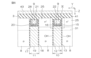
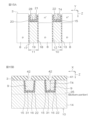
- FIG. 1 is a schematic cross-sectional perspective view showing a partial region of a semiconductor device according to a first embodiment of the present disclosure.
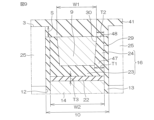
- FIG. 2 is a diagram in which the structure on the first main surface of the chip is removed from FIG. 1.
- FIG. 3 is a diagram from FIG. 2 with the emitter contact electrode layer removed.
- FIG. 4 is a schematic plan view of FIG. 3 viewed from the first main surface of the chip.
- FIG. 5 is a sectional view taken along the line VV shown in FIG. 4.
- FIG. 6 is a cross-sectional view taken along line VI-VI shown in FIG. 4.
- 7 is a cross-sectional perspective view taken along line VII-VII shown in FIG. 3.
- FIG. FIG. 8 is a cross-sectional view taken along line VIII-VIII shown in FIG. 4.
- FIG. 9 is an enlarged view of the portion surrounded by the two-dot chain line IX in FIG.
- FIGS. 10A and 10B are diagrams showing a part of the manufacturing process of the semiconductor device.
- FIGS. 11A and 11B are diagrams showing steps after FIGS. 10A and 10B, respectively.
- FIGS. 12A and 12B are diagrams showing steps after FIGS. 11A and 11B, respectively.
- FIGS. 13A and 13B are diagrams showing steps after FIGS. 12A and 12B, respectively.
- FIGS. 14A and 14B are diagrams showing steps after FIGS. 13A and 13B, respectively.
- FIGS. 15A and 15B are diagrams showing steps after FIGS. 14A and 14B, respectively.
- FIGS. 16A and 16B are diagrams showing steps after FIGS. 15A and 15B, respectively.
- FIGS. 17A and 17B are diagrams showing steps after FIGS. 16A and 16B, respectively.
- FIG. 18 is a schematic cross-sectional view showing a partial region of a semiconductor device according to a second embodiment of the present disclosure.
- FIG. 19 is a schematic cross-sectional view showing a partial region of a semiconductor device according to a second embodiment of the present disclosure.
- FIG. 20 is a schematic cross-sectional view showing a partial region of a semiconductor device according to a second embodiment of the present disclosure.
- FIG. 21 is a schematic cross-sectional perspective view showing a partial region of a semiconductor device according to a third embodiment of the present disclosure.
- FIG. 22 is a schematic cross-sectional perspective view showing a partial region of a semiconductor device according to a fourth embodiment of the present disclosure.
- FIG. 23 is a diagram illustrating the steps involved in forming the structure of FIG. 22.
- FIG. 1 is a schematic cross-sectional perspective view showing a partial region of a semiconductor device 1 according to a first embodiment of the present disclosure.
- FIG. 2 is a diagram in which the structure on the first main surface 3 of the chip 2 is removed from FIG. 1.
- FIG. 3 is a diagram from FIG. 2 with the emitter contact electrode layer 51 removed.
- FIG. 4 is a schematic plan view of FIG. 3 viewed from the first main surface 3 of the chip 2.
- FIG. 5 is a sectional view taken along the line VV shown in FIG. 4.
- FIG. 6 is a cross-sectional view taken along line VI-VI shown in FIG. 4.
- 7 is a cross-sectional perspective view taken along line VII-VII shown in FIG. 3.
- FIG. 8 is a cross-sectional view taken along line VIII-VIII shown in FIG. 4.
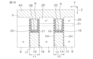
- FIG. 9 is an enlarged view of the portion surrounded by the two-dot chain line IX in FIG. 5, 6 and 8 also illustrate the structure on the first main surface 3 of the chip 2.
- the semiconductor device 1 has a basic configuration including a trench gate type IGBT (Insulated Gate Bipolar Transistor).
- semiconductor device 1 includes an n ⁇ type chip 2.
- the chip 2 is made of an n - type silicon single crystal substrate.
- the silicon single crystal substrate is formed using an n - type silicon single crystal semiconductor wafer manufactured through the FZ (Floating Zone) method.
- the chip 2 may be called a semiconductor chip or a semiconductor layer.
- the chip 2 has a first main surface 3 on one side and a second main surface 4 on the other side.
- the thickness of the chip 2 may be 50 ⁇ m or more and 300 ⁇ m or less.
- the thickness of the chip 2 may be 50 ⁇ m or more and 100 ⁇ m or less, 100 ⁇ m or more and 150 ⁇ m or less, 150 ⁇ m or more and 200 ⁇ m or less, 200 ⁇ m or more and 250 ⁇ m or less, or 250 ⁇ m or more and 300 ⁇ m or less.
- a p-type collector region 5 is formed on the surface portion of the second main surface 4.
- An n-type charge storage region 6 is formed in the surface portion of the first main surface 3 .
- the charge storage region 6 is formed at a distance from the collector region 5 on the first main surface 3 side.
- an n ⁇ type drift region 7 is formed in a region between a collector region 5 and a charge storage region 6 in chip 2. As shown in FIG. Drift region 7 is formed by a region located between collector region 5 and charge storage region 6 in chip 2 . A p-type body region 8 is formed on the surface of the charge storage region 6 . A plurality of trench gate electrode structures 10 and a plurality of trench emitter electrode structures 11 are formed at intervals on the surface portion of the first main surface 3.
- FIGS. 1 to 7 only one trench gate electrode structure 10 and one trench emitter electrode structure 11 adjacent to each other are shown.
- the structure of the semiconductor device 1 will be described below, focusing on the structure of one trench gate electrode structure 10 and one trench emitter electrode structure 11.
- the trench gate electrode structure 10 and the trench emitter electrode structure 11 extend in a band shape along an arbitrary first direction X in plan view.
- the trench gate electrode structure 10 and the trench emitter electrode structure 11 are formed at intervals along a second direction Y that intersects the first direction X.
- planar view refers to a planar view seen from the normal direction Z of the first principal surface 3 (hereinafter simply referred to as "normal direction Z"). More specifically, the second direction Y is a direction perpendicular to the first direction X. The first direction X and the second direction Y are also tangential directions of the first main surface 3.
- the trench pitch P0 between the trench gate electrode structure 10 and the trench emitter electrode structure 11 may be 0.1 ⁇ m or more and less than 0.6 ⁇ m.
- Trench pitch P0 is 0.1 ⁇ m or more and 0.2 ⁇ m or less, 0.2 ⁇ m or more and 0.3 ⁇ m or less, 0.3 ⁇ m or more and 0.4 ⁇ m or less, 0.4 ⁇ m or more and 0.5 ⁇ m or less, or 0.5 ⁇ m or more and 0.6 ⁇ m It may be less than
- the trench pitch P0 is preferably 0.2 ⁇ m or more and 0.4 ⁇ m or less (for example, about 0.25 ⁇ m).
- the trench gate electrode structure 10 includes a gate trench 12, a gate insulating layer 13, a gate electrode layer 14, a plurality of gate electrode recesses 15, a plurality of gate covering insulating layers 16, a plurality of gate buried bodies 9, and a plurality of gate intermediate insulating layers 22. including.
- Gate trench 12 extends from first main surface 3 through body region 8 and charge storage region 6 to drift region 7 .
- the depth of the gate trench 12 may be 2.0 ⁇ m or more and 4.0 ⁇ m or less.
- the depth of the gate trench 12 may be 2.0 ⁇ m or more and 2.5 ⁇ m or less, 2.5 ⁇ m or more and 3.0 ⁇ m or less, 3.0 ⁇ m or more and 3.5 ⁇ m or less, or 3.5 ⁇ m or more and 4.0 ⁇ m or less.
- the depth of the gate trench 12 is preferably 2.5 ⁇ m or more and 3.5 ⁇ m or less (for example, about 3.0 ⁇ m).
- the width of the gate trench 12 in the second direction may be 0.5 ⁇ m or more and 1.5 ⁇ m or less.
- the width of the gate trench 12 in the second direction is 0.5 ⁇ m or more and 0.75 ⁇ m or less, 0.75 ⁇ m or more and 1.0 ⁇ m or less, 1.0 ⁇ m or more and 1.25 ⁇ m or less, or 1.25 ⁇ m or more and 1.5 ⁇ m or less. Good too.
- the width of the gate trench 12 in the second direction is preferably 0.5 ⁇ m or more and 1.0 ⁇ m or less (for example, about 0.75 ⁇ m).
- the gate insulating layer 13 may be formed of silicon oxide.
- the gate insulating layer 13 is formed in a film shape along the inner wall of the gate trench 12 .
- Gate insulating layer 13 defines a concave space within gate trench 12 .
- the gate electrode layer 14 may be formed of conductive polysilicon. Gate electrode layer 14 is controlled by gate voltage. The gate electrode layer 14 is embedded in the gate trench 12 with the gate insulating layer 13 in between. More specifically, the gate electrode layer 14 is embedded in a concave space defined by the gate insulating layer 13 within the gate trench 12 .
- the plurality of gate electrode recesses 15 are formed on the upper surface of the gate electrode layer 14 at intervals along the first direction X.
- the upper end portion of the gate electrode layer 14 has an uneven structure including a plurality of gate electrode recesses 15.
- the interval between the plurality of gate electrode recesses 15 adjacent to each other may be greater than 0 ⁇ m and less than or equal to 10 ⁇ m.
- the interval between the plurality of gate electrode recesses 15 adjacent to each other is also the width in the first direction X of a portion of the gate electrode layer 14 sandwiched between two gate electrode recesses 15 adjacent to each other.
- the interval between the plurality of gate electrode recesses 15 adjacent to each other may be more than 0 ⁇ m and less than 2 ⁇ m, more than 2 ⁇ m and less than 4 ⁇ m, more than 4 ⁇ m and less than 6 ⁇ m, more than 6 ⁇ m and less than 8 ⁇ m, or more than 8 ⁇ m and less than 10 ⁇ m.
- each gate electrode recess 15 are formed by the gate insulating layer 13 and the gate electrode layer 14.
- a pair of side walls facing each other in the first direction X are formed of the gate electrode layer 14, and a pair of side walls facing each other in the second direction Y are formed of the gate insulating layer 13.
- the bottom wall of each gate electrode recess 15 is formed by the gate electrode layer 14. Referring to FIG. 8, the bottom wall of each gate electrode recess 15 may be located in a region between the first main surface 3 and the bottom of an emitter region 25 (described later) with respect to the normal direction Z, or It may be located deeper than the bottom of the emitter region 25.
- each gate electrode recess 15 is formed in a tapered shape with a bottom area smaller than the opening area.
- the angle ⁇ formed by the upper surface of the gate electrode layer 14 and the side wall of the gate electrode recess 15 within the gate electrode layer 14 may be more than 90° and less than or equal to 120° (for example, about 102°).
- a plurality of gate covering insulating layers 16 are formed within the gate trench 12 on the upper surface of the gate electrode layer 14 and on the sidewalls of the gate electrode recess 15. More specifically, the plurality of gate covering insulating layers 16 are formed independently in the plurality of gate electrode recesses 15. Each gate covering insulating layer 16 covers the gate electrode layer 14 within the gate trench 12, is formed along the sidewall of the gate electrode recess 15, and is exposed from the opening of the gate trench 12. Each gate covering insulating layer 16 defines a concave space in each gate electrode concave portion 15 . The concave space within the gate electrode recess 15 is surrounded by a gate covering insulating layer 16 from below and from the sides.
- gate covering insulating layer 16 includes a bottom portion 23 that covers the upper surface of gate electrode layer 14, and a side portion 24 that extends upward from bottom portion 23 along the sidewall of gate trench 12.
- the bottom portion 23 of the gate covering insulating layer 16 has a thickness of 150 nm or more and 300 nm or less.
- the side portion 24 of the gate covering insulating layer 16 has a first thickness T1 at a lower end portion 47 in the depth direction of the gate trench 12, and has a first thickness T1 at an upper end portion 48 in the depth direction of the gate trench 12. It has a second thickness T2 that is thinner than the thickness T1.
- the first thickness T1 is, for example, 300 nm or less, and the second thickness T2 is, for example, 50 nm or less. Further, the width W1 of the upper end of the gate buried body 9 may be narrower than the width W2 of the upper end of the gate electrode layer 14.
- an outer side surface 29 on the side closer to the side wall of the gate trench 12 and an inner side surface 30 on the opposite side to the outer side surface 29 are located at the lower end of the gate covering insulating layer 16 . They have a tapered shape that slopes closer to each other from 47 toward the upper end 48.
- a step S may be formed between the upper end of the side portion 24 of the gate covering insulating layer 16 and the first main surface 3. In other words, the upper end of the side portion 24 of the gate covering insulating layer 16 may be located at a lower height position with respect to the first main surface 3 in the depth direction of the gate trench 12.
- the plurality of gate embedded bodies 9 may be formed of the same material as the gate electrode layer 14. That is, the plurality of gate buried bodies 9 may be formed of conductive polysilicon. Although the gate buried body 9 has conductivity, it may be electrically floating in this embodiment.
- the gate buried body 9 is buried in the gate electrode recess 15 with the gate covering insulating layer 16 in between. More specifically, the gate buried body 9 is buried in a concave space defined by the gate covering insulating layer 16 in the gate electrode concave portion 15 .
- the plurality of gate intermediate insulating layers 22 may be formed of silicon oxide. Each gate intermediate insulating layer 22 is interposed between the gate electrode layer 14 and the gate covering insulating layer 16 within each gate electrode recess 15 . Referring to FIG. 9, gate intermediate insulating layer 22 is formed between the upper surface of gate electrode layer 14 and the bottom portion 23 of gate covering insulating layer 16 in this embodiment.
- the thickness of the gate intermediate insulating layer 22 (third thickness T3) may be, for example, 20 nm or more and 150 nm or less.
- the gate intermediate insulating layer 22 is clearly distinguished from the gate covering insulating layer 16 (bottom portion 23) in the figure. Depending on the conditions of the manufacturing process, it may not be distinguished from the gate covering insulating layer 16 and may be integrated with the gate covering insulating layer 16 in appearance.
- the trench emitter electrode structure 11 includes an emitter trench 17, an emitter insulating layer 18, an emitter electrode layer 19, an emitter electrode recess 20, an emitter covering insulating layer 21, an emitter buried body 27, and an emitter intermediate insulating layer 28.
- Emitter trench 17 extends from first main surface 3 through body region 8 and charge storage region 6 to drift region 7 .
- the depth of the emitter trench 17 may be 2.0 ⁇ m or more and 4.0 ⁇ m or less.
- the depth of the emitter trench 17 may be 2.0 ⁇ m or more and 2.5 ⁇ m or less, 2.5 ⁇ m or more and 3.0 ⁇ m or less, 3.0 ⁇ m or more and 3.5 ⁇ m or less, or 3.5 ⁇ m or more and 4.0 ⁇ m or less.
- the depth of the emitter trench 17 is preferably 2.5 ⁇ m or more and 3.5 ⁇ m or less (for example, about 3.0 ⁇ m).
- the depth of emitter trench 17 is approximately equal to the depth of gate trench 12.
- the width of the emitter trench 17 in the second direction may be 0.5 ⁇ m or more and 1.5 ⁇ m or less.
- the width in the second direction of the emitter trench 17 is 0.5 ⁇ m or more and 0.75 ⁇ m or less, 0.75 ⁇ m or more and 1.0 ⁇ m or less, 1.0 ⁇ m or more and 1.25 ⁇ m or less, or 1.25 ⁇ m or more and 1.5 ⁇ m or less.
- the width of the emitter trench 17 in the second direction is preferably 0.5 ⁇ m or more and 1.0 ⁇ m or less (for example, about 0.75 ⁇ m).
- the width of the emitter trench 17 in the second direction is preferably approximately equal to the width of the gate trench 12 in the second direction.
- the emitter insulating layer 18 may be formed of silicon oxide. Emitter insulating layer 18 is formed in a film shape along the inner wall of emitter trench 17 . Emitter insulating layer 18 defines a concave space within emitter trench 17 .
- the emitter electrode layer 19 may be formed of conductive polysilicon. Emitter electrode layer 19 is controlled by emitter voltage. The emitter voltage has a voltage value less than the gate voltage. The emitter voltage may be a reference voltage (eg, ground voltage). Emitter electrode layer 19 is embedded in emitter trench 17 with emitter insulating layer 18 in between. More specifically, the emitter electrode layer 19 is embedded in a concave space defined by the emitter insulating layer 18 in the emitter trench 17 .
- the emitter electrode recess 20 is formed so as to dig down almost the entire upper surface of the emitter electrode layer 19. In other words, the emitter electrode layer 19 is buried halfway in the depth direction of the concave space defined by the emitter insulating layer 18 .
- the side walls of the emitter electrode recess 20 are formed by the emitter insulating layer 18 in this embodiment.
- the bottom wall of the emitter electrode recess 20 is formed by the emitter electrode layer 19.
- the bottom wall of the emitter electrode recess 20 may be located in a region between the first main surface 3 and the bottom of the emitter region 25 (described later) with respect to the normal direction Z. However, it may be located deeper than the bottom of the emitter region 25. That is, the upper end of the emitter electrode layer 19 is located on the first main surface 3 side with respect to the bottom of the emitter region 25 (described later). With respect to the normal direction Z, the depth of the emitter electrode recess 20 may be approximately equal to the depth of the gate electrode recess 15.
- the emitter covering insulating layer 21 is formed on the upper surface of the emitter electrode layer 19 and the sidewall of the emitter electrode recess 20 in the emitter trench 17 . That is, the emitter covering insulating layer 21 is formed along the inner wall of the emitter electrode recess 20. The emitter covering insulating layer 21 covers the emitter electrode layer 19 within the emitter trench 17 , is formed along the sidewall of the emitter electrode recess 20 , and is exposed from the opening of the emitter trench 17 . The emitter covering insulating layer 21 defines a concave space in the emitter electrode concave portion 20 . The concave space within the emitter electrode recess 20 is surrounded by an emitter covering insulating layer 21 from below and from the sides. Although the description will be omitted, the emitter covering insulating layer 21 has the same cross-sectional shape as the gate covering insulating layer 16 shown in FIG.
- the emitter buried body 27 may be formed of the same material as the emitter electrode layer 19. That is, the emitter buried body 27 may be formed of conductive polysilicon.
- the emitter embedding body 27 is electrically conductive, but may be electrically floating in this embodiment.
- the emitter embedding body 27 is embedded in the emitter electrode recess 20 with the emitter covering insulating layer 21 in between. More specifically, the emitter embedding body 27 is embedded in a concave space defined by the emitter coating insulating layer 21 within the emitter electrode concave portion 20 .
- the emitter intermediate insulating layer 28 may be formed of silicon oxide.
- the emitter intermediate insulating layer 28 is interposed between the emitter electrode layer 19 and the emitter covering insulating layer 21 within the emitter electrode recess 20 .
- n + type emitter region 25 (impurity region) is formed in a region along the sidewall of the gate trench 12 in the surface portion of the body region 8 . More specifically, a plurality of emitter regions 25 are formed along one sidewall and the other sidewall of the gate trench 12 in the first direction X. The plurality of emitter regions 25 are each formed in a band shape extending along the first direction X. Emitter region 25 is in contact with the sidewall of gate trench 12 . Emitter region 25 is also in contact with the sidewall of emitter trench 17 .
- an emitter region 25 In the region along the sidewall of the gate trench 12 in the surface portion of the first main surface 3, from the first main surface 3 toward the second main surface 4 side, there is an emitter region 25, a body region 8, a charge storage region 6, and a drift region. Regions 7 are formed in this order.
- An IGBT channel CH is formed in the body region 8 in a region facing the gate electrode layer 14 with the gate insulating layer 13 in between.
- a plurality of contact trenches 31 are formed in the surface portion of first main surface 3. As shown in FIG. The plurality of contact trenches 31 are formed at intervals along the first direction X. The plurality of contact trenches 31 are each formed in a band shape extending along the second direction Y. The width of each contact trench 31 in the first direction is smaller than the width of the gate trench 12 in the second direction.
- each contact trench 31 extends from the inner region of the corresponding gate covering insulating layer 16 through the side wall of the gate trench 12 to the surface portion of the first main surface 3.
- each contact trench 31 passes through one sidewall and the other sidewall of the gate trench 12 from the inner region of the gate covering insulating layer 16 in the second direction Y.
- Each contact trench 31 includes a first intersection region 33 that intersects with the gate electrode layer 14 in plan view.
- the bottom wall of each contact trench 31 is formed by the gate covering insulating layer 16
- the side wall of each contact trench 31 is formed by the gate filling body 9 .
- Each contact trench 31 includes a second intersection region 34 that intersects with the emitter electrode layer 19 in plan view.
- the bottom wall of each contact trench 31 is formed by the emitter covering insulating layer 21
- the side wall of each contact trench 31 is formed by the emitter buried body 27 .
- Each contact trench 31 further includes a contact region 35 drawn out from the first intersection region 33 to the outside of the gate trench 12 .
- Contact region 35 may be referred to as a connection region that connects first intersection region 33 and second intersection region 34 in a region between gate trench 12 and emitter trench 17 in plan view.
- the bottom wall of each contact trench 31 is formed by body region 8
- the side wall of each contact trench 31 is formed by body region 8 and emitter region 25 . That is, in the contact region 35, the stacked structure of the body region 8 and the emitter region 25 is exposed on the side wall of the contact trench 31.
- Each contact trench 31 further has a drawn-out portion 32 drawn out from one side wall of the emitter trench 17.
- Each lead-out portion 32 penetrates from the surface portion of the first main surface 3 through one side wall of the emitter trench 17 and reaches into the emitter trench 17 .
- the first depth D1 from the first main surface 3 to the upper surface of the gate electrode layer 14 in the first intersection region 33 is shallower than the second depth D2 of the contact trench 31 in the contact region 35. . Therefore, the contact trench 31 has an uneven structure in which the gate electrode layer 14 and the emitter electrode layer 19 selectively protrude in the second direction Y.
- the first depth D1 is 1 ⁇ m or less, preferably 0.5 ⁇ m or more and 1 ⁇ m or less.
- the second depth D2 is 0.3 ⁇ m or more and 1.0 ⁇ m or less.
- the upper end of the gate electrode layer 14 is located on the first main surface 3 side with respect to the bottom of the emitter region 25.
- the gate electrode layer 14 has opposing portions 40 that face the emitter region 25 with the gate insulating layer 13 in between, near both sides of the first intersection region 33 in the first direction X.
- the opposing portion 40 is a region indicated by horizontal hatching in FIG.
- the opposing portion 40 is located below the pair of gate embedded bodies 9 in the normal direction Z.
- the contact trench 31 includes a first bottom wall 37 in the first intersection region 33 and the second intersection region 34 , and a second bottom wall 38 in the contact region 35 and the lead-out portion 32 .
- a step 39 is formed between the first bottom wall 37 and the second bottom wall 38 due to the difference between the first depth D1 and the second depth D2.
- the arrangement of the plurality of contact trenches 31 is arbitrary.
- the plurality of contact trenches 31 may be formed at equal intervals along the first direction X.
- the plurality of contact trenches 31 may be formed at unequal intervals along the first direction X.
- a p + type contact region 36 is formed in a region along the bottom wall of each contact trench 31 in the body region 8 .
- Contact region 36 may be formed in a region along the bottom wall and side wall of each contact trench 31 in body region 8 .
- the contact region 36 is formed in a region deeper than the emitter region 25 in the body region 8 in the normal direction Z.
- the contact region 36 has an exposed surface exposed from the bottom wall of the contact trench 31.
- the exposed surface of the contact region 36 is formed in a region between the first main surface 3 and the bottom of the body region 8 . More specifically, the exposed surface of the contact region 36 is formed in a region between the bottom of the body region 8 and the bottom of the emitter region 25. More specifically, the exposed surface of the contact region 36 is formed below the upper surface of the gate electrode layer 14 and the upper surface of the emitter electrode layer 19.
- Interlayer insulating layer 41 is formed on the first main surface 3.
- Interlayer insulating layer 41 covers trench gate electrode structure 10 and trench emitter electrode structure 11 .
- Interlayer insulating layer 41 covers gate covering insulating layer 16 and gate buried body 9 exposed from gate trench 12, and emitter covering insulating layer 21 and emitter buried body 27 exposed from emitter trench 17.
- Interlayer insulating layer 41 may be formed of silicon oxide or silicon nitride.
- the interlayer insulating layer 41 may have a laminated structure including an oxide film (SiO 2 film) and a nitride film (SiN film).
- the oxide film (SiO 2 film) may include an NSG (Nondoped Silicon Glass) film that does not contain impurities and/or a PSG (Phosphorus Silicon Glass) film that contains phosphorus.
- the interlayer insulating layer 41 may have a stacked structure including an NSG film and a PSG film stacked in this order from the first main surface 3.
- the thickness of the NSG film may be greater than or equal to 2000 ⁇ and less than or equal to 8000 ⁇ (for example, approximately 5000 ⁇ ).
- the thickness of the PSG film may be greater than or equal to 2000 ⁇ and less than or equal to 6000 ⁇ (for example, about 4000 ⁇ ).
- a plurality of contact holes 42 are formed in the interlayer insulating layer 41. Each of the plurality of contact holes 42 communicates with the corresponding contact trench 31 . That is, the plurality of contact holes 42 are formed at intervals along the first direction X, and are each formed in a band shape extending along the second direction Y.
- the plurality of contact holes 42 penetrate the interlayer insulating layer 41 and communicate with the corresponding contact trenches 31, respectively. Thereby, the plurality of contact holes 42 form one emitter contact trench 31, 42 with the corresponding contact trench 31.
- the width of each contact hole 42 in the first direction may be greater than or equal to the width of each contact trench 31 in the first direction. That is, the width of each contact hole 42 in the first direction may be equal to the width of each contact trench 31 in the first direction, or may exceed the width of each contact trench 31 in the first direction.
- the inner wall of each contact hole 42 may surround the inner wall of the corresponding contact trench 31.
- the arrangement of the plurality of contact holes 42 is arbitrary and adjusted according to the arrangement of the contact trenches 31.
- the plurality of contact holes 42 may be formed at equal intervals along the first direction X.
- the plurality of contact holes 42 may be formed at unequal intervals along the first direction X.
- An emitter main surface electrode layer 43 is formed on the interlayer insulating layer 41. Emitter main surface electrode layer 43 enters contact hole 42 and contact trench 31 (that is, emitter contact trenches 31 and 42) from above interlayer insulating layer 41.
- the emitter main surface electrode layer 43 may include, for example, a laminated structure of a barrier layer made of titanium or the like and an electrode layer made of tungsten or the like.
- a plurality of emitter contact electrode layers 51 are formed by portions of the emitter main surface electrode layer 43 located within the plurality of contact trenches 31 . As a result, a structure in which a plurality of emitter contact electrode layers 51 are embedded in the surface portion of the chip 2 is formed.
- the plurality of emitter contact electrode layers 51 each have an arrangement and shape corresponding to the arrangement and shape of the plurality of contact trenches 31. That is, the plurality of emitter contact electrode layers 51 are formed at intervals along the first direction X, and are each formed in a band shape extending along the second direction Y.
- Each emitter contact electrode layer 51 faces the gate electrode layer 14 with the gate covering insulating layer 16 in between with respect to the normal direction Z and the first direction are doing.
- Each emitter contact electrode layer 51 is insulated from gate electrode layer 14 by gate covering insulating layer 16 .
- a gate buried body 9 is interposed between the emitter contact electrode layer 51 and the gate covering insulating layer 16.
- the gate buried bodies 9 are provided on both sides of the first intersection region 33 in the first direction It includes a pair of gate embedded bodies 9 sandwiched from the sides. Therefore, in the first intersection region 33, the emitter contact electrode layer 51 is in direct contact with the gate covering insulating layer 16 in the normal direction Z, and in contact with the gate buried body 9 in the first direction X.
- the emitter contact electrode layer 51 is surrounded from three sides by the lower gate covering insulating layer 16 and the gate filling bodies 9 on both sides.
- Each emitter contact electrode layer 51 faces the emitter electrode layer 19 with the emitter covering insulating layer 21 in between with respect to the normal direction Z and the first direction are doing.
- Each emitter contact electrode layer 51 is insulated from emitter electrode layer 19 by emitter covering insulating layer 21 .
- an emitter buried body 27 is interposed between the emitter contact electrode layer 51 and the emitter covering insulating layer 21.
- the emitter embedded bodies 27 are provided on both sides of the second intersection region 34 in the first direction It includes a pair of emitter embedding bodies 27 which are sandwiched from the sides. Therefore, in the second intersection region 34, the emitter contact electrode layer 51 is in direct contact with the emitter covering insulating layer 21 in the normal direction Z, and in contact with the emitter buried body 27 in the first direction X.
- the emitter contact electrode layer 51 is surrounded from three sides by the emitter covering insulating layer 21 below and the emitter buried bodies 27 on both sides.
- a collector electrode layer 61 is formed on the second main surface 4 of the chip 2. Collector electrode layer 61 is connected to collector region 5 .
- a gate main surface electrode layer having the same structure as the emitter main surface electrode layer 43 may be formed on the interlayer insulating layer 41. The gate main surface electrode layer may be electrically connected to the gate electrode layer 14 through a gate contact hole formed in the interlayer insulating layer 41.
- FIGS. 10A, 10B to 17A, 17B are diagrams showing part of the manufacturing process of the semiconductor device 1 in order of process.
- the drawings marked with “A” correspond to the cross-sections in FIG. 5
- the drawings marked with "B” correspond to the cross-sections in FIG. 8. ing.
- an n ⁇ type semiconductor wafer 26 is prepared.
- the semiconductor wafer 26 has the first main surface 3 and the second main surface 4 (not shown) of the chip 2 described above.
- a p-type collector region 5 (not shown) and an n-type charge storage region 6 are formed in the semiconductor wafer 26.
- Collector region 5 is formed by introducing p-type impurities into second main surface 4 of semiconductor wafer 26 .
- the collector region 5 may be formed on the surface portion of the second main surface 4 of the semiconductor wafer 26 by an ion implantation method using an ion implantation mask (not shown).
- Charge storage region 6 is formed by introducing n-type impurities into first main surface 3 .
- the charge storage region 6 may be formed on the surface portion of the first main surface 3 by an ion implantation method using an ion implantation mask (not shown).
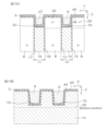
- unnecessary portions of the semiconductor wafer 26 are selectively removed from the first main surface 3 through a mask having a predetermined pattern. Unnecessary portions of the semiconductor wafer 26 may be removed by an etching method (for example, a wet etching method). As a result, gate trench 12 and emitter trench 17 are formed. The mask is then removed. Next, gate insulating layer 13 and emitter insulating layer 18 are formed on the inner walls of gate trench 12 and emitter trench 17, respectively, by thermal oxidation or wet oxidation, for example. Next, gate electrode layer 14 and emitter electrode layer 19 are buried in gate trench 12 and emitter trench 17, respectively, by, for example, the CVD method. As a result, a trench gate electrode structure 10 and a trench emitter electrode structure 11 are formed.
- an etching method for example, a wet etching method
- gate electrode layer 14 and emitter electrode layer 19 are selectively removed from first main surface 3 through a mask having a predetermined pattern. As a result, gate electrode recess 15 and emitter electrode recess 20 are formed.
- the unnecessary portions of the gate electrode layer 14 and the unnecessary portions of the emitter electrode layer 19 may be removed by an etching method (for example, a wet etching method).
- a first base insulating layer 44 will be the base of the gate intermediate insulating layer 22 and the emitter intermediate insulating layer 28, and a first base insulating layer 44 will be the base of the gate covering insulating layer 16 and the emitter covering insulating layer 21.
- a second base insulating layer 45 is formed.
- the first base insulating layer 44 may be formed, for example, by thermal oxidation treatment of the surfaces of the gate electrode layer 14 and emitter electrode layer 19 and the surface of the semiconductor wafer 26.
- the second base insulating layer 45 may be formed by depositing an insulating material on the first base insulating layer 44 by, for example, a CVD method.
- the first base insulating layer 44 and the second base insulating layer 45 are formed in the gate trench 12 and the emitter trench 17, and are also formed to cover the first main surface 3 of the semiconductor wafer 26.
- a polysilicon layer that will become the base of gate buried body 9 and emitter buried body 27 is deposited over the entire first main surface 3 by, for example, the CVD method. Thereafter, the polysilicon layer is planarized by etching back to obtain a gate buried body 9 and an emitter buried body 27 buried in the gate electrode recess 15 and the emitter electrode recess 20, respectively.
- Body region 8 is formed by introducing p-type impurities into first main surface 3 .
- Body region 8 may be formed on the surface portion of first main surface 3 by ion implantation using an ion implantation mask (not shown).
- Emitter region 25 is formed by introducing n-type impurities into first main surface 3 .
- the emitter region 25 may be formed on the surface portion of the first main surface 3 by an ion implantation method using an ion implantation mask (not shown).
- interlayer insulating layer 41 is formed on first main surface 3.
- Interlayer insulating layer 41 is formed on first main surface 3 to cover trench gate electrode structure 10 and trench emitter electrode structure 11 .
- This step may include a step of forming an NSG film (for example, 5000 ⁇ ) and a PSG film (for example, 4000 ⁇ ) on the first main surface 3 in this order by the CVD method.
- unnecessary parts of interlayer insulating layer 41, unnecessary parts of gate covering insulating layer 16, and unnecessary parts of emitter covering insulating layer 21 are removed through a mask having a predetermined pattern. Selectively removed. Unnecessary portions such as the interlayer insulating layer 41 may be removed by an etching method (for example, a dry etching method). As a result, a contact hole 42 is formed.
- unnecessary portions of the semiconductor wafer 26 are removed through the mask used when forming the contact holes 42.
- the unnecessary portion of the semiconductor wafer 26 may be removed by, for example, an etching method (for example, a dry etching method).
- a contact trench 31 is formed in the first main surface 3.
- FIG. 16A the structure visible on the back side of the contact trench 31 is shown by broken line hatching.
- the gate buried body 9 is also etched at the same time when the contact trench 31 is formed. Further, the second depth D2 of the contact trench 31 is larger than the thickness T4 of the gate buried body 9 (see FIGS. 15A and 15B). Therefore, in the first intersection region 33 , the gate buried body 9 is etched so that the gate buried body 9 penetrates from the first main surface 3 to the bottom wall of the gate electrode recess 15 .
- a contact region 36 is formed on the surface portion of the first main surface 3. More specifically, contact region 36 is formed in a region along the bottom wall of contact trench 31 in the surface layer portion of body region 8 . Contact region 36 may be formed in a region along the sidewall and bottom wall of contact trench 31. Contact region 36 is formed by introducing p-type impurities into contact trench 31 . Contact region 36 may be introduced into contact trench 31 by ion implantation through an ion implantation mask (not shown). As a result, a contact region 36 along the bottom wall of the contact trench 31 is formed.
- emitter main surface electrode layer 43 is formed on interlayer insulating layer 41.
- the emitter main surface electrode layer 43 may be formed by a sputtering method or a CVD method.
- the emitter contact electrode layer 51 is formed by the portion of the emitter main surface electrode layer 43 that enters the contact trench 31 .
- a collector electrode layer 61 is formed on the second main surface 4 of the semiconductor wafer 26 .
- the gate buried body 9 is formed of polysilicon, and has an etching selectivity with respect to the interlayer insulating layer 41 made of silicon oxide or silicon nitride.
- the gate buried body 9 having an etching selectivity with respect to the interlayer insulating layer 41 means, for example, the etching ratio shown by the ratio of the etching amount (a) of the interlayer insulating layer 41 to the etching amount (b) of the gate buried body 9.
- the selectivity ratio (a/b) is, for example, 1.5 or more, preferably 5 or more, and more preferably 10 or more.
- the gate embedded body 9 can be used as an etching stopper. It is possible to prevent the gate intermediate insulating layer 22 from being exposed to etching gas when forming the contact hole 42. Therefore, the thickness of the gate intermediate insulating layer 22 can be easily controlled to a designed value by the formation conditions of the gate intermediate insulating layer 22 (for example, thermal oxidation conditions, CVD conditions, etc.). Therefore, short circuits between the gate electrode layer 14 and the emitter contact electrode layer 51 and reduction in TZDB (Time Zero Dielectric Breakdown) are prevented, and the controllability of the capacitance between the gate electrode layer 14 and the emitter contact electrode layer 51 is improved. can be improved.
- TZDB Time Zero Dielectric Breakdown
- the gate intermediate insulating layer 22 is not etched when forming the contact hole 42. Therefore, it is not necessary to form the gate intermediate insulating layer 22 excessively thick in order to prevent a short circuit between the gate and the emitter due to over-etching of the gate intermediate insulating layer 22. Furthermore, there is no need to form the gate electrode recess 15 deeply in order to form the thick gate intermediate insulating layer 22. As a result, the gate electrode recess 15 can be formed relatively shallowly, so that the facing portion 40 of the gate electrode layer 14 facing the emitter region 25 with the gate insulating layer 13 interposed in the vicinity of both sides of the first intersection region 33 can be formed relatively shallowly. can be secured.
- a region near the first intersection region 33 can be used as a channel forming region 46 (see FIG. 3), so that reduction in channel width can be suppressed. Therefore, it is possible to provide a semiconductor device 1 that can reduce on-resistance.
- FIG. 18 is a schematic cross-sectional view showing a partial region of a semiconductor device 71 according to a second embodiment of the present disclosure.
- FIG. 19 is a schematic cross-sectional view showing a partial region of a semiconductor device 71 according to a second embodiment of the present disclosure.
- FIG. 20 is a schematic cross-sectional view showing a partial region of the semiconductor device 71 according to the second embodiment of the present disclosure. 18 corresponds to the cross section of FIG. 5, FIG. 19 corresponds to the cross section of FIG. 6, and FIG. 20 corresponds to the cross section of FIG.
- structures corresponding to those described for the semiconductor device 1 according to the first embodiment will be given the same reference numerals and descriptions will be omitted.
- the first depth D1 from the first main surface 3 to the upper surface of the gate electrode layer 14 in the first intersection region 33 is the depth of the contact trench 31 in the contact region 35. is deeper than the second depth D2.
- a stacked structure of the gate covering insulating layer 16 and the gate buried body 9 is formed on the bottom wall of the contact trench 31 .
- the gate buried body 9 is formed so as to span from one side of the first intersection region 33 in the first direction X to the other side, and the emitter contact electrode layer 51 is It surrounds from both sides and from below.
- the upper end of the gate electrode layer 14 is located on the second main surface 4 side (opposite the first main surface 3) with respect to the bottom of the emitter region 25. Therefore, in the semiconductor device 71 according to the second embodiment, the opposing portion 40 shown in FIG. It does not face the emitter region 25 via.
- the semiconductor device 71 according to the second embodiment can also achieve the same effects as those described for the semiconductor device 1.
- the semiconductor device 71 can be manufactured by simply changing the depth of the gate electrode recess 15 and the depth of the emitter electrode recess 20 in the method of manufacturing the semiconductor device 1.
- FIG. 21 is a schematic cross-sectional perspective view showing a partial region of a semiconductor device 81 according to a third embodiment of the present disclosure.
- structures corresponding to those described for the semiconductor device 1 will be given the same reference numerals and descriptions will be omitted.
- the semiconductor device 1 described above an example has been described in which the p-type collector region 5 is formed on the surface portion of the second main surface 4.
- an n-type drain region 82 is formed on the surface of the second main surface 4 instead of the p-type collector region 5 .
- the semiconductor device 81 has a basic configuration including a trench gate type MISFET (Metal Insulator Semiconductor Field Effect Transistor).
- MISFET Metal Insulator Semiconductor Field Effect Transistor
- the semiconductor device 81 can also achieve the same effects as those described for the semiconductor device 1.
- the semiconductor device 81 can be manufactured by simply forming an n-type drain region 82 in place of the p-type collector region 5 and changing the layout of each mask in the method for manufacturing the semiconductor device 1.
- FIG. 22 is a schematic cross-sectional perspective view showing a partial region of a semiconductor device 91 according to a fourth embodiment of the present disclosure.
- FIG. 23 is a diagram illustrating the steps involved in forming the structure of FIG. 22. 22 and 23 show cross sections of the above-described semiconductor device 1 corresponding to FIG. 9. In the following, structures corresponding to those described for the semiconductor device 1 will be given the same reference numerals and descriptions will be omitted.
- the width W1 of the upper end of the gate buried body 9 is narrower than the width W2 of the upper end of the gate electrode layer 14.
- the width W1 of the upper end of the gate buried body 9 is wider than the width W2 of the upper end of the gate electrode layer 14.
- the gate trench 12 is formed in a tapered shape with a bottom area smaller than an opening area.
- the angle ⁇ 2 formed by the side wall of the gate trench 12 with respect to a plane 92 parallel to the first main surface 3 may be, for example, more than 80° and less than 90°, preferably more than 85° and less than 90°. good. Therefore, in the depth direction of the gate trench 12, the width W1 of the gate buried body 9 formed at a position closer to the open end of the gate trench 12 than the depth position of the gate electrode layer 14 is the width W2 of the gate electrode layer 14. becomes wider than
- the side portion 24 of the gate covering insulating layer 16 has the upper end portion 48 having a second thickness T2 that is thinner than the first thickness T1 of the lower end portion 47.
- the second thickness T2 may be 0 (zero) because the outer side surface 29 and the inner side surface 30 are in contact with each other at the upper end portion 48.
- the upper end portion 48 of the side portion 24 of the gate covering insulating layer 16 may be a sharp tip pointing upward.
- the semiconductor device 91 can also achieve the same effects as those described for the semiconductor device 1.
- the semiconductor device 91 is manufactured in the method for manufacturing the semiconductor device 1 by forming the gate trench 12 by etching to form a tapered shape and forming the side portions 24 of the gate covering insulating layer 16 so as to have a tapered shape. can.
- the mesa structure 93 of the chip 2 (the part where the emitter region 25 and the like are formed) formed on the side of the gate trench 12 is trapezoidal and round in cross-sectional view. It may have a formed upper end 94.
- the width W1 of the gate buried body 9 can be made wider than the width W2 of the gate electrode layer 14.
- a structure may be adopted in which the conductivity type of each semiconductor portion is inverted. That is, the p-type portion may be made into the n-type, and the n-type portion may be made into the p-type.
- chip 2 is made of silicon single crystal.
- chip 2 may also include SiC.
- the chip 2 may be made of SiC single crystal.
- the gate trench (12) is formed on the first main surface (3) so as to cover the gate electrode (14) and extends along a second direction (Y) intersecting the first direction (X).
- the surface insulating layer (41) having a contact hole (42) drawn out from the upper region to the outside of the gate trench (12); electrically connected to the body region (8) and the first impurity region (25) through the contact hole (42), and from inside the gate trench (12) through the sidewall of the gate trench (12).
- a semiconductor device (1) including a buried body (9) buried in a region above the covering insulating layer (16) in the gate trench (12) and having an etching selectivity with respect to the surface insulating layer (41). , 71, 81).
- the covering insulating layer (16) has a bottom part (23) that covers the upper surface of the gate electrode (14), and a side part (24) that extends upward from the bottom part (23) along the side wall of the gate trench (12). )
- Appendix 1-3 The semiconductor device (1, 71, 81) according to appendix 1-2, wherein the bottom portion (23) of the covering insulating layer (16) has a thickness of 150 nm or more and 300 nm or less.
- the side portion (24) of the covering insulating layer (16) has a first thickness (T1) at a lower end portion (47) in the depth direction of the gate trench (12), and
- the side portion (24) of the covering insulating layer (16) includes an outer side surface (29) on the side closer to the side wall of the gate trench (12) and an inner side surface on the opposite side to the outer side surface (29).
- (30) has a tapered shape that is inclined toward each other from the lower end (47) to the upper end (48), according to any one of Supplementary notes 1-2 to 1-4. (1, 71, 81).
- the body region (8) is formed at least along the bottom wall (37, 38) of the contact trench (31),
- the first impurity region (25) is formed at least along the sidewall of the contact trench (31), Supplementary Note 1, wherein the contact electrode (51) is embedded in the contact trench (31) and connected to the body region (8) and the first impurity region (25) inside the contact trench (31).
- the semiconductor device (1, 71, 81) according to any one of -1 to Supplementary Note 1-5.
- the contact trench (31) has an intersection region (33) that intersects with the gate trench (12), is drawn out from the intersection region (33) to the outside of the gate trench (12), and is connected to the body region (8) and the intersection region (33). a contact region (35) in which the first impurity region (25) is exposed;
- the depth (D1) from the first main surface (3) in the intersection region (33) to the upper surface of the gate electrode (14) is the depth (D1) from the first main surface (3) in the contact region (35) to the top surface of the gate electrode (14).
- the semiconductor device (1, 81) according to appendix 1-6, which is shallower than the depth (D2) to the bottom wall of the contact trench (31).
- the depth (D1) from the first main surface (3) to the upper surface of the gate electrode (14) in the intersection region (33) is 1 ⁇ m or less, according to Appendix 1-7 or 1-8.
- the contact trench (31) has an intersection region (33) that intersects with the gate trench (12), is drawn out from the intersection region (33) to the outside of the gate trench (12), and is connected to the body region (8) and the intersection region (33). a contact region in which the first impurity region (25) is exposed;
- the depth (D1) from the first main surface (3) in the intersection region (33) to the upper surface of the gate electrode (14) is the depth (D1) from the first main surface (3) in the contact region to the contact trench (
- the semiconductor device (71) according to appendix 1-6 which is deeper than the depth (D2) to the bottom wall of 31).
- the bottom wall (37) of the contact trench (31) is formed with a laminated structure of the bottom (23) of the covering insulating layer (16) and the embedded body (9).
- the embedded body (9) is formed so as to span from one side to the other side of the intersection region (33) in the first direction (X), and connects the contact electrode (51) with the intersection region (33) in the first direction (X).
- the semiconductor device (71) according to appendix 1-10 which is surrounded from both sides and from three directions below.
- the surface insulating layer (41) is made of silicon oxide, The semiconductor device (1, 71, 81) according to any one of attachments 1-1 to 1-12, wherein the gate electrode (14) and the buried body (9) are formed of polysilicon.
- a contact trench (31) is formed in the surface portion of the first main surface (3) so that the body region (8) and the first impurity region (25) are exposed by etching through the contact hole (42). a step of forming; forming a contact electrode (51) connected to the body region (8) and the first impurity so as to be embedded in the contact trench (31), The method for manufacturing a semiconductor device (1, 71, 81), wherein the embedded body (9) is formed of a material having an etching selectivity with respect to the surface insulating layer (41).
Abstract
Provided is a semiconductor device including: a gate electrode embedded in a gate trench; a surface insulating layer that is formed on a first principal surface and that has a contact hole; a covering insulating layer that covers the gate electrode in the gate trench and that insulates the gate electrode from a contact electrode; and an embedded body that is embedded in a region on the covering insulating layer in the gate trench and that has etching selectivity with respect to the surface insulating layer.
Description
本出願は、2022年9月9日に日本国特許庁に提出された特願2022-143915号に対応しており、この出願の全開示はここに引用により組み込まれるものとする。
This application corresponds to Japanese Patent Application No. 2022-143915 filed with the Japan Patent Office on September 9, 2022, and the entire disclosure of this application is hereby incorporated by reference.
本開示は、半導体装置およびその製造方法に関する。
The present disclosure relates to a semiconductor device and a method for manufacturing the same.
特許文献1は、トレンチが形成された主面を有する半導体層と、前記半導体層の前記主面の表層部において前記トレンチの側壁に沿って形成された第1導電型のボディ領域と、前記ボディ領域の表層部において前記トレンチの側壁に沿って形成された第2導電型の不純物領域と、前記トレンチの内壁に形成されたゲート絶縁層と、前記トレンチに埋め込まれ、前記ゲート絶縁層を挟んで前記ボディ領域および前記不純物領域と対向するゲート電極と、前記トレンチ内から前記トレンチの側壁を貫通して前記半導体層の前記主面の表層部に引き出され、前記ボディ領域および前記不純物領域に電気的に接続されたコンタクト電極と、前記トレンチ内において前記ゲート電極および前記コンタクト電極の間に介在し、前記ゲート電極および前記コンタクト電極を絶縁する埋め込み絶縁層とを含む、半導体装置を開示している。
Patent Document 1 discloses a semiconductor layer having a main surface in which a trench is formed, a body region of a first conductivity type formed along a side wall of the trench in a surface layer portion of the main surface of the semiconductor layer, and a body region of the body. a second conductivity type impurity region formed along the sidewalls of the trench in the surface layer of the region; a gate insulating layer formed on the inner wall of the trench; and an impurity region buried in the trench and sandwiching the gate insulating layer. A gate electrode facing the body region and the impurity region and a gate electrode extending from within the trench through the sidewall of the trench to a surface layer portion of the main surface of the semiconductor layer and electrically connected to the body region and the impurity region. A semiconductor device is disclosed, including a contact electrode connected to the trench, and a buried insulating layer interposed between the gate electrode and the contact electrode in the trench and insulating the gate electrode and the contact electrode.
本開示の一実施形態は、ゲート電極とコンタクト電極との間の容量の制御性を向上することができる半導体装置およびその製造方法を提供する。
An embodiment of the present disclosure provides a semiconductor device and a method for manufacturing the same that can improve controllability of capacitance between a gate electrode and a contact electrode.
本開示の一実施形態は、ゲートトレンチに交差するコンタクトトレンチを含む構造において、チャネル幅の縮小を抑制し、オン抵抗を低減することができる半導体装置およびその製造方法を提供する。
An embodiment of the present disclosure provides a semiconductor device and a method for manufacturing the same that can suppress reduction in channel width and reduce on-resistance in a structure including a contact trench intersecting a gate trench.
本開示の一実施形態に係る半導体装置は、第1方向に延びるゲートトレンチが形成された第1主面を有するチップと、前記第1主面の表面部において前記ゲートトレンチの側壁に沿って形成された第1導電型のボディ領域と、前記ボディ領域の表面部において前記ゲートトレンチの側壁に沿って形成された第2導電型の第1不純物領域と、前記ゲートトレンチの内壁に形成されたゲート絶縁層と、前記ゲートトレンチに埋め込まれ、前記ゲート絶縁層を挟んで前記ボディ領域および前記第1不純物領域に対向するゲート電極と、前記ゲート電極を被覆するように前記第1主面上に形成され、かつ前記第1方向に交差する第2方向に沿って前記ゲートトレンチ上の領域から前記ゲートトレンチの外側に引き出されたコンタクト孔を有する前記表面絶縁層と、前記コンタクト孔を介して前記ボディ領域および前記第1不純物領域に電気的に接続され、かつ前記ゲートトレンチ内から前記ゲートトレンチの側壁を介して前記第1主面の表面部に引き出されたコンタクト電極と、前記ゲートトレンチ内において前記ゲート電極を被覆し、前記ゲート電極と前記コンタクト電極との間を絶縁する被覆絶縁層と、前記ゲートトレンチ内における前記被覆絶縁層上の領域に埋め込まれ、前記表面絶縁層に対してエッチング選択比を有する埋め込み体とを含む。
A semiconductor device according to an embodiment of the present disclosure includes a chip having a first main surface in which a gate trench extending in a first direction is formed, and a gate trench formed along a sidewall of the gate trench in a surface portion of the first main surface. a first impurity region of a second conductivity type formed along a side wall of the gate trench in a surface portion of the body region; and a gate formed on an inner wall of the gate trench. an insulating layer, a gate electrode embedded in the gate trench and facing the body region and the first impurity region with the gate insulating layer in between, and formed on the first main surface so as to cover the gate electrode. and a contact hole extending from a region above the gate trench to the outside of the gate trench along a second direction intersecting the first direction; a contact electrode electrically connected to the first impurity region and the first impurity region and drawn out from within the gate trench to a surface portion of the first main surface through a sidewall of the gate trench; a covering insulating layer that covers the gate electrode and insulates between the gate electrode and the contact electrode; and a covering insulating layer that is embedded in a region on the covering insulating layer in the gate trench and has an etching selectivity with respect to the surface insulating layer. and an embedded body having a.
本開示の一実施形態に係る半導体装置の製造方法は、ゲートトレンチが形成された第1主面を有する半導体ウエハの前記ゲートトレンチの内壁にゲート絶縁層を形成する工程と、前記ゲート絶縁層の形成後、前記ゲートトレンチにゲート電極を埋め込む工程と、前記ゲート電極を上面側から選択的に除去することによって、前記ゲートトレンチ内に凹部を形成する工程と、前記ゲート電極の上面を被覆するように、前記凹部内に被覆絶縁層を形成する工程と、前記凹部内における前記被覆絶縁層上の領域に、埋め込み体を埋め込む工程と、前記第1主面の表面部に選択的に第1導電型の不純物を注入することによって、前記ゲートトレンチの側壁に沿ってボディ領域を形成する工程と、前記ボディ領域の表面部に選択的に第2導電型の不純物を注入することによって、前記ゲートトレンチの側壁に沿って第1不純物領域を形成する工程と、前記ゲート電極および前記埋め込み体を被覆するように、前記第1主面上に表面絶縁層を形成する工程と、前記表面絶縁層を選択的にエッチングすることによって、前記埋め込み体および前記第1主面が選択的に露出するように、前記ゲートトレンチに交差するコンタクト孔を形成する工程と、前記コンタクト孔を介したエッチングによって、前記ボディ領域および前記第1不純物領域が露出するように、前記第1主面の表面部にコンタクトトレンチを形成する工程と、前記コンタクトトレンチに埋め込まれるように、前記ボディ領域および前記第1不純物に接続されるコンタクト電極を形成する工程とを含み、前記埋め込み体は、前記表面絶縁層に対してエッチング選択比を有する材料により形成されている。
A method for manufacturing a semiconductor device according to an embodiment of the present disclosure includes the steps of: forming a gate insulating layer on the inner wall of the gate trench of a semiconductor wafer having a first main surface on which a gate trench is formed; After the formation, a step of embedding the gate electrode in the gate trench, a step of forming a recess in the gate trench by selectively removing the gate electrode from the upper surface side, and a step of covering the upper surface of the gate electrode. forming an insulating cover layer in the recess; embedding an embedding body in a region on the insulating cover layer in the recess; and selectively applying a first conductive layer to a surface portion of the first main surface. forming a body region along the sidewall of the gate trench by implanting an impurity of a second conductivity type; forming a first impurity region along a sidewall of the gate electrode, forming a surface insulating layer on the first main surface so as to cover the gate electrode and the embedded body, and selecting the surface insulating layer. forming a contact hole intersecting the gate trench so that the embedded body and the first main surface are selectively exposed by selectively etching the body; forming a contact trench in a surface portion of the first main surface so that the region and the first impurity region are exposed; the buried body is formed of a material having an etching selectivity with respect to the surface insulating layer.
本開示の一実施形態によれば、埋め込み体は、表面絶縁層に対してエッチング選択比を有する材料により形成されている。これにより、表面絶縁層にコンタクト孔を形成する際に埋め込み体をエッチングストップ層として利用できるので、被覆絶縁層がエッチングされることを防止することができる。したがって、被覆絶縁層の厚さを、被覆絶縁層の形成時の設計値として簡単に制御することができる。よって、ゲート電極とコンタクト電極との間のショートやTZDB(Time Zero Dielectric Breakdown)の低下を防ぐとともに、ゲート電極とコンタクト電極との間の容量の制御性を向上することができる。
According to one embodiment of the present disclosure, the embedded body is formed of a material that has an etching selectivity with respect to the surface insulating layer. Thereby, the embedded body can be used as an etching stop layer when forming a contact hole in the surface insulating layer, so that the covering insulating layer can be prevented from being etched. Therefore, the thickness of the insulating cover layer can be easily controlled as a design value when forming the insulating cover layer. Therefore, short circuits between the gate electrode and the contact electrode and reduction in TZDB (Time Zero Dielectric Breakdown) can be prevented, and controllability of the capacitance between the gate electrode and the contact electrode can be improved.
次に、本開示の実施形態を、添付図面を参照して詳細に説明する。
Next, embodiments of the present disclosure will be described in detail with reference to the accompanying drawings.
図1は、本開示の第1実施形態に係る半導体装置1の一部の領域を示す模式的な断面斜視図である。図2は、図1からチップ2の第1主面3の上の構造を取り除いた図である。図3は、図2からエミッタコンタクト電極層51を取り除いた図である。
FIG. 1 is a schematic cross-sectional perspective view showing a partial region of a semiconductor device 1 according to a first embodiment of the present disclosure. FIG. 2 is a diagram in which the structure on the first main surface 3 of the chip 2 is removed from FIG. 1. FIG. 3 is a diagram from FIG. 2 with the emitter contact electrode layer 51 removed.
図4は、図3をチップ2の第1主面3から見た模式的な平面図である。図5は、図4に示すV-V線に沿う断面図である。図6は、図4に示すVI-VI線に沿う断面図である。図7は、図3に示すVII-VII線に沿う断面斜視図である。図8は、図4に示すVIII-VIII線に沿う断面図である。図9は、図6の二点鎖線IXで囲まれた部分の拡大図である。図5、図6および図8では、チップ2の第1主面3の上の構造も図示している。
FIG. 4 is a schematic plan view of FIG. 3 viewed from the first main surface 3 of the chip 2. FIG. 5 is a sectional view taken along the line VV shown in FIG. 4. FIG. 6 is a cross-sectional view taken along line VI-VI shown in FIG. 4. 7 is a cross-sectional perspective view taken along line VII-VII shown in FIG. 3. FIG. FIG. 8 is a cross-sectional view taken along line VIII-VIII shown in FIG. 4. FIG. 9 is an enlarged view of the portion surrounded by the two-dot chain line IX in FIG. 5, 6 and 8 also illustrate the structure on the first main surface 3 of the chip 2.
半導体装置1は、この実施形態では、トレンチゲート型のIGBT(Insulated Gate Bipolar Transistor)を備えた基本形態を有している。図1~図3を参照して、半導体装置1は、n-型のチップ2を含む。チップ2は、この実施形態では、n-型のシリコン単結晶基板からなる。シリコン単結晶基板は、FZ(Floating Zone)法を経て製造されたn-型のシリコン単結晶の半導体ウエハを用いて形成されている。チップ2は、半導体チップと称されてもよいし、半導体層と称されてもよい。
In this embodiment, the semiconductor device 1 has a basic configuration including a trench gate type IGBT (Insulated Gate Bipolar Transistor). Referring to FIGS. 1 to 3, semiconductor device 1 includes an n − type chip 2. Referring to FIGS. In this embodiment, the chip 2 is made of an n - type silicon single crystal substrate. The silicon single crystal substrate is formed using an n - type silicon single crystal semiconductor wafer manufactured through the FZ (Floating Zone) method. The chip 2 may be called a semiconductor chip or a semiconductor layer.
チップ2は、一方側の第1主面3および他方側の第2主面4を有している。チップ2の厚さは、50μm以上300μm以下であってもよい。チップ2の厚さは、50μm以上100μm以下、100μm以上150μm以下、150μm以上200μm以下、200μm以上250μm以下、または、250μm以上300μm以下であってもよい。
The chip 2 has a first main surface 3 on one side and a second main surface 4 on the other side. The thickness of the chip 2 may be 50 μm or more and 300 μm or less. The thickness of the chip 2 may be 50 μm or more and 100 μm or less, 100 μm or more and 150 μm or less, 150 μm or more and 200 μm or less, 200 μm or more and 250 μm or less, or 250 μm or more and 300 μm or less.
図1~図3を参照して、第2主面4の表面部には、p型のコレクタ領域5が形成されている。第1主面3の表面部には、n型の電荷蓄積領域6が形成されている。電荷蓄積領域6は、コレクタ領域5に対して第1主面3側に間隔を空けて形成されている。
Referring to FIGS. 1 to 3, a p-type collector region 5 is formed on the surface portion of the second main surface 4. An n-type charge storage region 6 is formed in the surface portion of the first main surface 3 . The charge storage region 6 is formed at a distance from the collector region 5 on the first main surface 3 side.
図1~図3を参照して、チップ2においてコレクタ領域5および電荷蓄積領域6の間の領域には、n-型のドリフト領域7が形成されている。ドリフト領域7は、チップ2においてコレクタ領域5および電荷蓄積領域6の間に位置する領域によって形成されている。電荷蓄積領域6の表面部には、p型のボディ領域8が形成されている。第1主面3の表面部には、複数のトレンチゲート電極構造10および複数のトレンチエミッタ電極構造11が間隔を空けて形成されている。
Referring to FIGS. 1 to 3, an n − type drift region 7 is formed in a region between a collector region 5 and a charge storage region 6 in chip 2. As shown in FIG. Drift region 7 is formed by a region located between collector region 5 and charge storage region 6 in chip 2 . A p-type body region 8 is formed on the surface of the charge storage region 6 . A plurality of trench gate electrode structures 10 and a plurality of trench emitter electrode structures 11 are formed at intervals on the surface portion of the first main surface 3.
図1~図7では、互いに隣り合う1つのトレンチゲート電極構造10および1つのトレンチエミッタ電極構造11だけが示されている。以下では、これら1つのトレンチゲート電極構造10および1つのトレンチエミッタ電極構造11の構造に着目して半導体装置1の構造について説明する。
In FIGS. 1 to 7, only one trench gate electrode structure 10 and one trench emitter electrode structure 11 adjacent to each other are shown. The structure of the semiconductor device 1 will be described below, focusing on the structure of one trench gate electrode structure 10 and one trench emitter electrode structure 11.
トレンチゲート電極構造10およびトレンチエミッタ電極構造11は、平面視において、任意の第1方向Xに沿って帯状に延びている。トレンチゲート電極構造10およびトレンチエミッタ電極構造11は、第1方向Xに交差する第2方向Yに沿って間隔を空けて形成されている。
The trench gate electrode structure 10 and the trench emitter electrode structure 11 extend in a band shape along an arbitrary first direction X in plan view. The trench gate electrode structure 10 and the trench emitter electrode structure 11 are formed at intervals along a second direction Y that intersects the first direction X.
平面視とは、より具体的には、第1主面3の法線方向Z(以下、単に「法線方向Z」という。)から見た平面視のことをいう。第2方向Yは、より具体的には、第1方向Xに直交する方向である。第1方向Xおよび第2方向Yは、第1主面3の接線方向でもある。
More specifically, the planar view refers to a planar view seen from the normal direction Z of the first principal surface 3 (hereinafter simply referred to as "normal direction Z"). More specifically, the second direction Y is a direction perpendicular to the first direction X. The first direction X and the second direction Y are also tangential directions of the first main surface 3.
トレンチゲート電極構造10およびトレンチエミッタ電極構造11の間のトレンチピッチP0は、0.1μm以上0.6μm未満であってもよい。トレンチピッチP0は、0.1μm以上0.2μm以下、0.2μm以上0.3μm以下、0.3μm以上0.4μm以下、0.4μm以上0.5μm以下、または、0.5μm以上0.6μm未満であってもよい。トレンチピッチP0は、0.2μm以上0.4μm以下(たとえば0.25μm程度)であることが好ましい。
The trench pitch P0 between the trench gate electrode structure 10 and the trench emitter electrode structure 11 may be 0.1 μm or more and less than 0.6 μm. Trench pitch P0 is 0.1 μm or more and 0.2 μm or less, 0.2 μm or more and 0.3 μm or less, 0.3 μm or more and 0.4 μm or less, 0.4 μm or more and 0.5 μm or less, or 0.5 μm or more and 0.6 μm It may be less than The trench pitch P0 is preferably 0.2 μm or more and 0.4 μm or less (for example, about 0.25 μm).
トレンチゲート電極構造10は、ゲートトレンチ12、ゲート絶縁層13、ゲート電極層14、複数のゲート電極凹部15、複数のゲート被覆絶縁層16、複数のゲート埋め込み体9および複数のゲート中間絶縁層22を含む。ゲートトレンチ12は、第1主面3からボディ領域8および電荷蓄積領域6を貫通してドリフト領域7に至る。
The trench gate electrode structure 10 includes a gate trench 12, a gate insulating layer 13, a gate electrode layer 14, a plurality of gate electrode recesses 15, a plurality of gate covering insulating layers 16, a plurality of gate buried bodies 9, and a plurality of gate intermediate insulating layers 22. including. Gate trench 12 extends from first main surface 3 through body region 8 and charge storage region 6 to drift region 7 .
ゲートトレンチ12の深さは、2.0μm以上4.0μm以下であってもよい。ゲートトレンチ12の深さは、2.0μm以上2.5μm以下、2.5μm以上3.0μm以下、3.0μm以上3.5μm以下、または、3.5μm以上4.0μm以下であってもよい。ゲートトレンチ12の深さは、2.5μm以上3.5μm以下(たとえば3.0μm程度)であることが好ましい。
The depth of the gate trench 12 may be 2.0 μm or more and 4.0 μm or less. The depth of the gate trench 12 may be 2.0 μm or more and 2.5 μm or less, 2.5 μm or more and 3.0 μm or less, 3.0 μm or more and 3.5 μm or less, or 3.5 μm or more and 4.0 μm or less. . The depth of the gate trench 12 is preferably 2.5 μm or more and 3.5 μm or less (for example, about 3.0 μm).
ゲートトレンチ12の第2方向幅は、0.5μm以上1.5μm以下であってもよい。ゲートトレンチ12の第2方向幅は、0.5μm以上0.75μm以下、0.75μm以上1.0μm以下、1.0μm以上1.25μm以下、または、1.25μm以上1.5μm以下であってもよい。ゲートトレンチ12の第2方向幅は、0.5μm以上1.0μm以下(たとえば0.75μm程度)であることが好ましい。
The width of the gate trench 12 in the second direction may be 0.5 μm or more and 1.5 μm or less. The width of the gate trench 12 in the second direction is 0.5 μm or more and 0.75 μm or less, 0.75 μm or more and 1.0 μm or less, 1.0 μm or more and 1.25 μm or less, or 1.25 μm or more and 1.5 μm or less. Good too. The width of the gate trench 12 in the second direction is preferably 0.5 μm or more and 1.0 μm or less (for example, about 0.75 μm).
ゲート絶縁層13は、酸化シリコンにより形成されていてもよい。ゲート絶縁層13は、ゲートトレンチ12の内壁に沿って膜状に形成されている。ゲート絶縁層13は、ゲートトレンチ12内において凹状の空間を区画している。
The gate insulating layer 13 may be formed of silicon oxide. The gate insulating layer 13 is formed in a film shape along the inner wall of the gate trench 12 . Gate insulating layer 13 defines a concave space within gate trench 12 .
ゲート電極層14は、導電性のポリシリコンにより形成されていてもよい。ゲート電極層14は、ゲート電圧によって制御される。ゲート電極層14は、ゲート絶縁層13を挟んでゲートトレンチ12に埋め込まれている。ゲート電極層14は、より具体的には、ゲートトレンチ12内においてゲート絶縁層13によって区画された凹状の空間に埋め込まれている。
The gate electrode layer 14 may be formed of conductive polysilicon. Gate electrode layer 14 is controlled by gate voltage. The gate electrode layer 14 is embedded in the gate trench 12 with the gate insulating layer 13 in between. More specifically, the gate electrode layer 14 is embedded in a concave space defined by the gate insulating layer 13 within the gate trench 12 .
複数のゲート電極凹部15は、この実施形態では、第1方向Xに沿って間隔を空けてゲート電極層14の上面に形成されている。これにより、ゲート電極層14の上端部は、複数のゲート電極凹部15を含む凹凸構造を有している。
In this embodiment, the plurality of gate electrode recesses 15 are formed on the upper surface of the gate electrode layer 14 at intervals along the first direction X. As a result, the upper end portion of the gate electrode layer 14 has an uneven structure including a plurality of gate electrode recesses 15.
互いに隣り合う複数のゲート電極凹部15の間隔は、0μmを超えて10μm以下であってもよい。互いに隣り合う複数のゲート電極凹部15の間隔は、ゲート電極層14において互いに隣り合う2つのゲート電極凹部15によって挟まれた部分の第1方向Xの幅でもある。互いに隣り合う複数のゲート電極凹部15の間隔は、0μmを超えて2μm以下、2μm以上4μm以下、4μm以上6μm以下、6μm以上8μm以下、または、8μm以上10μm以下であってもよい。
The interval between the plurality of gate electrode recesses 15 adjacent to each other may be greater than 0 μm and less than or equal to 10 μm. The interval between the plurality of gate electrode recesses 15 adjacent to each other is also the width in the first direction X of a portion of the gate electrode layer 14 sandwiched between two gate electrode recesses 15 adjacent to each other. The interval between the plurality of gate electrode recesses 15 adjacent to each other may be more than 0 μm and less than 2 μm, more than 2 μm and less than 4 μm, more than 4 μm and less than 6 μm, more than 6 μm and less than 8 μm, or more than 8 μm and less than 10 μm.
各ゲート電極凹部15の側壁は、この実施形態では、ゲート絶縁層13およびゲート電極層14により形成されている。第1方向Xにおいて対向する一対の側壁がゲート電極層14により形成され、第2方向Yにおいて対向する一対の側壁がゲート絶縁層13により形成されている。各ゲート電極凹部15の底壁は、ゲート電極層14により形成されている。図8を参照して、各ゲート電極凹部15の底壁は、法線方向Zに関して、第1主面3およびエミッタ領域25(後述)の底部の間の領域に位置していてもよいし、エミッタ領域25の底部よりも深い部分に位置していてもよい。
In this embodiment, the side walls of each gate electrode recess 15 are formed by the gate insulating layer 13 and the gate electrode layer 14. A pair of side walls facing each other in the first direction X are formed of the gate electrode layer 14, and a pair of side walls facing each other in the second direction Y are formed of the gate insulating layer 13. The bottom wall of each gate electrode recess 15 is formed by the gate electrode layer 14. Referring to FIG. 8, the bottom wall of each gate electrode recess 15 may be located in a region between the first main surface 3 and the bottom of an emitter region 25 (described later) with respect to the normal direction Z, or It may be located deeper than the bottom of the emitter region 25.
図8を参照して、各ゲート電極凹部15は、底面積が開口面積よりも小さいテーパ形状に形成されている。ゲート電極層14の上面およびゲート電極凹部15の側壁がゲート電極層14内において成す角度θは、90°を超えて120°以下(たとえば102°程度)であってもよい。
Referring to FIG. 8, each gate electrode recess 15 is formed in a tapered shape with a bottom area smaller than the opening area. The angle θ formed by the upper surface of the gate electrode layer 14 and the side wall of the gate electrode recess 15 within the gate electrode layer 14 may be more than 90° and less than or equal to 120° (for example, about 102°).
複数のゲート被覆絶縁層16は、ゲートトレンチ12内においてゲート電極層14の上面およびゲート電極凹部15の側壁に形成されている。複数のゲート被覆絶縁層16は、より具体的には、複数のゲート電極凹部15にそれぞれ独立して形成されている。各ゲート被覆絶縁層16は、ゲートトレンチ12内でゲート電極層14を被覆し、かつゲート電極凹部15の側壁に沿って形成され、ゲートトレンチ12の開口から露出している。各ゲート被覆絶縁層16は、各ゲート電極凹部15において、凹状の空間を区画している。当該ゲート電極凹部15内の凹状の空間は、下方および側方からゲート被覆絶縁層16に取り囲まれている。
A plurality of gate covering insulating layers 16 are formed within the gate trench 12 on the upper surface of the gate electrode layer 14 and on the sidewalls of the gate electrode recess 15. More specifically, the plurality of gate covering insulating layers 16 are formed independently in the plurality of gate electrode recesses 15. Each gate covering insulating layer 16 covers the gate electrode layer 14 within the gate trench 12, is formed along the sidewall of the gate electrode recess 15, and is exposed from the opening of the gate trench 12. Each gate covering insulating layer 16 defines a concave space in each gate electrode concave portion 15 . The concave space within the gate electrode recess 15 is surrounded by a gate covering insulating layer 16 from below and from the sides.
図9を参照して、ゲート被覆絶縁層16は、ゲート電極層14の上面を被覆する底部23と、底部23からゲートトレンチ12の側壁に沿って上方に延びる側部24とを含む。ゲート被覆絶縁層16の底部23は、150nm以上300nm以下の厚さを有している。一方、ゲート被覆絶縁層16の側部24は、ゲートトレンチ12の深さ方向における下端部47に第1厚さT1を有し、ゲートトレンチ12の深さ方向における上端部48に、第1厚さT1よりも薄い第2厚さT2を有している。第1厚さT1は、たとえば、300nm以下であり、第2厚さT2は、たとえば、50nm以下である。また、ゲート埋め込み体9の上端部の幅W1は、ゲート電極層14の上端部の幅W2よりも狭くてもよい。
Referring to FIG. 9, gate covering insulating layer 16 includes a bottom portion 23 that covers the upper surface of gate electrode layer 14, and a side portion 24 that extends upward from bottom portion 23 along the sidewall of gate trench 12. The bottom portion 23 of the gate covering insulating layer 16 has a thickness of 150 nm or more and 300 nm or less. On the other hand, the side portion 24 of the gate covering insulating layer 16 has a first thickness T1 at a lower end portion 47 in the depth direction of the gate trench 12, and has a first thickness T1 at an upper end portion 48 in the depth direction of the gate trench 12. It has a second thickness T2 that is thinner than the thickness T1. The first thickness T1 is, for example, 300 nm or less, and the second thickness T2 is, for example, 50 nm or less. Further, the width W1 of the upper end of the gate buried body 9 may be narrower than the width W2 of the upper end of the gate electrode layer 14.
ゲート被覆絶縁層16の側部24は、断面視において、ゲートトレンチ12の側壁に近い側の外側側面29と、外側側面29の反対側の内側側面30とが、ゲート被覆絶縁層16の下端部47から上端部48に向かって互いに近づくように傾斜するテーパ形状を有している。ゲート被覆絶縁層16の側部24の上端と第1主面3との間には、段差Sが形成されていてもよい。換言すると、ゲート被覆絶縁層16の側部24の上端は、第1主面3に対してゲートトレンチ12の深さ方向に低い高さ位置に配置されていてもよい。
In the side portion 24 of the gate covering insulating layer 16 , in cross-sectional view, an outer side surface 29 on the side closer to the side wall of the gate trench 12 and an inner side surface 30 on the opposite side to the outer side surface 29 are located at the lower end of the gate covering insulating layer 16 . They have a tapered shape that slopes closer to each other from 47 toward the upper end 48. A step S may be formed between the upper end of the side portion 24 of the gate covering insulating layer 16 and the first main surface 3. In other words, the upper end of the side portion 24 of the gate covering insulating layer 16 may be located at a lower height position with respect to the first main surface 3 in the depth direction of the gate trench 12.
複数のゲート埋め込み体9は、この実施形態では、ゲート電極層14と同じ材料により形成されていてもよい。つまり、複数のゲート埋め込み体9は、導電性のポリシリコンにより形成されていてもよい。ゲート埋め込み体9は、導電性を有するが、この実施形態では電気的にフローティングされていてもよい。ゲート埋め込み体9は、ゲート被覆絶縁層16を挟んでゲート電極凹部15に埋め込まれている。ゲート埋め込み体9は、より具体的には、ゲート電極凹部15内においてゲート被覆絶縁層16によって区画された凹状の空間に埋め込まれている。
In this embodiment, the plurality of gate embedded bodies 9 may be formed of the same material as the gate electrode layer 14. That is, the plurality of gate buried bodies 9 may be formed of conductive polysilicon. Although the gate buried body 9 has conductivity, it may be electrically floating in this embodiment. The gate buried body 9 is buried in the gate electrode recess 15 with the gate covering insulating layer 16 in between. More specifically, the gate buried body 9 is buried in a concave space defined by the gate covering insulating layer 16 in the gate electrode concave portion 15 .
複数のゲート中間絶縁層22は、酸化シリコンにより形成されていてもよい。各ゲート中間絶縁層22は、各ゲート電極凹部15内においてゲート電極層14とゲート被覆絶縁層16との間に介在されている。図9を参照して、ゲート中間絶縁層22は、この実施形態では、ゲート電極層14の上面とゲート被覆絶縁層16の底部23との間に形成されている。ゲート中間絶縁層22の厚さ(第3厚さT3)は、たとえば、20nm以上150nm以下であってもよい。ゲート中間絶縁層22は、図ではゲート被覆絶縁層16(底部23)と明確に区別されている。製造プロセスの条件によっては、ゲート被覆絶縁層16と区別されず、外観上においてゲート被覆絶縁層16と一体であってもよい。
The plurality of gate intermediate insulating layers 22 may be formed of silicon oxide. Each gate intermediate insulating layer 22 is interposed between the gate electrode layer 14 and the gate covering insulating layer 16 within each gate electrode recess 15 . Referring to FIG. 9, gate intermediate insulating layer 22 is formed between the upper surface of gate electrode layer 14 and the bottom portion 23 of gate covering insulating layer 16 in this embodiment. The thickness of the gate intermediate insulating layer 22 (third thickness T3) may be, for example, 20 nm or more and 150 nm or less. The gate intermediate insulating layer 22 is clearly distinguished from the gate covering insulating layer 16 (bottom portion 23) in the figure. Depending on the conditions of the manufacturing process, it may not be distinguished from the gate covering insulating layer 16 and may be integrated with the gate covering insulating layer 16 in appearance.
トレンチエミッタ電極構造11は、エミッタトレンチ17、エミッタ絶縁層18、エミッタ電極層19、エミッタ電極凹部20、エミッタ被覆絶縁層21、エミッタ埋め込み体27およびエミッタ中間絶縁層28を含む。エミッタトレンチ17は、第1主面3からボディ領域8および電荷蓄積領域6を貫通してドリフト領域7に至る。
The trench emitter electrode structure 11 includes an emitter trench 17, an emitter insulating layer 18, an emitter electrode layer 19, an emitter electrode recess 20, an emitter covering insulating layer 21, an emitter buried body 27, and an emitter intermediate insulating layer 28. Emitter trench 17 extends from first main surface 3 through body region 8 and charge storage region 6 to drift region 7 .
エミッタトレンチ17の深さは、2.0μm以上4.0μm以下であってもよい。エミッタトレンチ17の深さは、2.0μm以上2.5μm以下、2.5μm以上3.0μm以下、3.0μm以上3.5μm以下、または、3.5μm以上4.0μm以下であってもよい。エミッタトレンチ17の深さは、2.5μm以上3.5μm以下(たとえば3.0μm程度)であることが好ましい。エミッタトレンチ17の深さは、ゲートトレンチ12の深さとほぼ等しいことが好ましい。
The depth of the emitter trench 17 may be 2.0 μm or more and 4.0 μm or less. The depth of the emitter trench 17 may be 2.0 μm or more and 2.5 μm or less, 2.5 μm or more and 3.0 μm or less, 3.0 μm or more and 3.5 μm or less, or 3.5 μm or more and 4.0 μm or less. . The depth of the emitter trench 17 is preferably 2.5 μm or more and 3.5 μm or less (for example, about 3.0 μm). Preferably, the depth of emitter trench 17 is approximately equal to the depth of gate trench 12.
エミッタトレンチ17の第2方向幅は、0.5μm以上1.5μm以下であってもよい。エミッタトレンチ17の第2方向幅は、0.5μm以上0.75μm以下、0.75μm以上1.0μm以下、1.0μm以上1.25μm以下、または、1.25μm以上1.5μm以下であってもよい。エミッタトレンチ17の第2方向幅は、0.5μm以上1.0μm以下(たとえば0.75μm程度)であることが好ましい。エミッタトレンチ17の第2方向幅は、ゲートトレンチ12の第2方向幅とほぼ等しいことが好ましい。
The width of the emitter trench 17 in the second direction may be 0.5 μm or more and 1.5 μm or less. The width in the second direction of the emitter trench 17 is 0.5 μm or more and 0.75 μm or less, 0.75 μm or more and 1.0 μm or less, 1.0 μm or more and 1.25 μm or less, or 1.25 μm or more and 1.5 μm or less. Good too. The width of the emitter trench 17 in the second direction is preferably 0.5 μm or more and 1.0 μm or less (for example, about 0.75 μm). The width of the emitter trench 17 in the second direction is preferably approximately equal to the width of the gate trench 12 in the second direction.
エミッタ絶縁層18は、酸化シリコンにより形成されていてもよい。エミッタ絶縁層18は、エミッタトレンチ17の内壁に沿って膜状に形成されている。エミッタ絶縁層18は、エミッタトレンチ17内において凹状の空間を区画している。
The emitter insulating layer 18 may be formed of silicon oxide. Emitter insulating layer 18 is formed in a film shape along the inner wall of emitter trench 17 . Emitter insulating layer 18 defines a concave space within emitter trench 17 .
エミッタ電極層19は、導電性のポリシリコンにより形成されていてもよい。エミッタ電極層19は、エミッタ電圧によって制御される。エミッタ電圧は、ゲート電圧未満の電圧値を有している。エミッタ電圧は、基準電圧(たとえばグランド電圧)であってもよい。エミッタ電極層19は、エミッタ絶縁層18を挟んでエミッタトレンチ17に埋め込まれている。エミッタ電極層19は、より具体的には、エミッタトレンチ17内においてエミッタ絶縁層18によって区画された凹状の空間に埋め込まれている。
The emitter electrode layer 19 may be formed of conductive polysilicon. Emitter electrode layer 19 is controlled by emitter voltage. The emitter voltage has a voltage value less than the gate voltage. The emitter voltage may be a reference voltage (eg, ground voltage). Emitter electrode layer 19 is embedded in emitter trench 17 with emitter insulating layer 18 in between. More specifically, the emitter electrode layer 19 is embedded in a concave space defined by the emitter insulating layer 18 in the emitter trench 17 .
エミッタ電極凹部20は、この実施形態では、エミッタ電極層19の上面のほぼ全面を掘り下げるように形成されている。換言すると、エミッタ電極層19は、エミッタ絶縁層18によって区画された凹状の空間の深さ方向途中部まで埋め込まれている。
In this embodiment, the emitter electrode recess 20 is formed so as to dig down almost the entire upper surface of the emitter electrode layer 19. In other words, the emitter electrode layer 19 is buried halfway in the depth direction of the concave space defined by the emitter insulating layer 18 .
エミッタ電極凹部20の側壁は、この実施形態では、エミッタ絶縁層18により形成されている。エミッタ電極凹部20の底壁は、エミッタ電極層19により形成されている。図5および図6を参照して、エミッタ電極凹部20の底壁は、法線方向Zに関して、第1主面3およびエミッタ領域25(後述)の底部の間の領域に位置していてもよいし、エミッタ領域25の底部よりも深い部分に位置していてもよい。つまり、エミッタ電極層19の上端部は、エミッタ領域25(後述)の底部に対して第1主面3側に位置している。法線方向Zに関して、エミッタ電極凹部20の深さは、ゲート電極凹部15の深さにほぼ等しくてもよい。
The side walls of the emitter electrode recess 20 are formed by the emitter insulating layer 18 in this embodiment. The bottom wall of the emitter electrode recess 20 is formed by the emitter electrode layer 19. Referring to FIGS. 5 and 6, the bottom wall of the emitter electrode recess 20 may be located in a region between the first main surface 3 and the bottom of the emitter region 25 (described later) with respect to the normal direction Z. However, it may be located deeper than the bottom of the emitter region 25. That is, the upper end of the emitter electrode layer 19 is located on the first main surface 3 side with respect to the bottom of the emitter region 25 (described later). With respect to the normal direction Z, the depth of the emitter electrode recess 20 may be approximately equal to the depth of the gate electrode recess 15.
エミッタ被覆絶縁層21は、エミッタトレンチ17内においてエミッタ電極層19の上面およびエミッタ電極凹部20の側壁に形成されている。つまり、エミッタ被覆絶縁層21は、エミッタ電極凹部20の内壁に沿って形成されている。エミッタ被覆絶縁層21は、エミッタトレンチ17内でエミッタ電極層19を被覆し、かつエミッタ電極凹部20の側壁に沿って形成され、エミッタトレンチ17の開口から露出している。エミッタ被覆絶縁層21は、エミッタ電極凹部20において、凹状の空間を区画している。当該エミッタ電極凹部20内の凹状の空間は、下方および側方からエミッタ被覆絶縁層21に取り囲まれている。説明を省略するが、エミッタ被覆絶縁層21は、図9に示すゲート被覆絶縁層16と同じ断面形状を有している。
The emitter covering insulating layer 21 is formed on the upper surface of the emitter electrode layer 19 and the sidewall of the emitter electrode recess 20 in the emitter trench 17 . That is, the emitter covering insulating layer 21 is formed along the inner wall of the emitter electrode recess 20. The emitter covering insulating layer 21 covers the emitter electrode layer 19 within the emitter trench 17 , is formed along the sidewall of the emitter electrode recess 20 , and is exposed from the opening of the emitter trench 17 . The emitter covering insulating layer 21 defines a concave space in the emitter electrode concave portion 20 . The concave space within the emitter electrode recess 20 is surrounded by an emitter covering insulating layer 21 from below and from the sides. Although the description will be omitted, the emitter covering insulating layer 21 has the same cross-sectional shape as the gate covering insulating layer 16 shown in FIG.
エミッタ埋め込み体27は、この実施形態では、エミッタ電極層19と同じ材料により形成されていてもよい。つまり、エミッタ埋め込み体27は、導電性のポリシリコンにより形成されていてもよい。エミッタ埋め込み体27は、導電性を有するが、この実施形態では電気的にフローティングされていてもよい。エミッタ埋め込み体27は、エミッタ被覆絶縁層21を挟んでエミッタ電極凹部20に埋め込まれている。エミッタ埋め込み体27は、より具体的には、エミッタ電極凹部20内においてエミッタ被覆絶縁層21によって区画された凹状の空間に埋め込まれている。
In this embodiment, the emitter buried body 27 may be formed of the same material as the emitter electrode layer 19. That is, the emitter buried body 27 may be formed of conductive polysilicon. The emitter embedding body 27 is electrically conductive, but may be electrically floating in this embodiment. The emitter embedding body 27 is embedded in the emitter electrode recess 20 with the emitter covering insulating layer 21 in between. More specifically, the emitter embedding body 27 is embedded in a concave space defined by the emitter coating insulating layer 21 within the emitter electrode concave portion 20 .
エミッタ中間絶縁層28は、酸化シリコンにより形成されていてもよい。エミッタ中間絶縁層28は、エミッタ電極凹部20内においてエミッタ電極層19とエミッタ被覆絶縁層21との間に介在されている。
The emitter intermediate insulating layer 28 may be formed of silicon oxide. The emitter intermediate insulating layer 28 is interposed between the emitter electrode layer 19 and the emitter covering insulating layer 21 within the emitter electrode recess 20 .
ボディ領域8の表面部においてゲートトレンチ12の側壁に沿う領域には、n+型のエミッタ領域25(不純物領域)が形成されている。エミッタ領域25は、より具体的には、第1方向Xに関して、ゲートトレンチ12の一方側の側壁および他方側の側壁に沿って複数形成されている。複数のエミッタ領域25は、第1方向Xに沿って延びる帯状にそれぞれ形成されている。エミッタ領域25は、ゲートトレンチ12の側壁に接している。エミッタ領域25は、エミッタトレンチ17の側壁にも接している。
An n + type emitter region 25 (impurity region) is formed in a region along the sidewall of the gate trench 12 in the surface portion of the body region 8 . More specifically, a plurality of emitter regions 25 are formed along one sidewall and the other sidewall of the gate trench 12 in the first direction X. The plurality of emitter regions 25 are each formed in a band shape extending along the first direction X. Emitter region 25 is in contact with the sidewall of gate trench 12 . Emitter region 25 is also in contact with the sidewall of emitter trench 17 .
第1主面3の表面部においてゲートトレンチ12の側壁に沿う領域には、第1主面3から第2主面4側に向けて、エミッタ領域25、ボディ領域8、電荷蓄積領域6およびドリフト領域7がこの順に形成されている。ボディ領域8においてゲート絶縁層13を挟んでゲート電極層14と対向する領域にIGBTのチャネルCHが形成される。
In the region along the sidewall of the gate trench 12 in the surface portion of the first main surface 3, from the first main surface 3 toward the second main surface 4 side, there is an emitter region 25, a body region 8, a charge storage region 6, and a drift region. Regions 7 are formed in this order. An IGBT channel CH is formed in the body region 8 in a region facing the gate electrode layer 14 with the gate insulating layer 13 in between.
図3~図6および図7を参照して、第1主面3の表面部には、複数のコンタクトトレンチ31が形成されている。複数のコンタクトトレンチ31は、第1方向Xに沿って間隔を空けて形成されている。複数のコンタクトトレンチ31は、第2方向Yに沿って延びる帯状にそれぞれ形成されている。各コンタクトトレンチ31の第1方向幅は、ゲートトレンチ12の第2方向幅よりも小さい。
Referring to FIGS. 3 to 6 and 7, a plurality of contact trenches 31 are formed in the surface portion of first main surface 3. As shown in FIG. The plurality of contact trenches 31 are formed at intervals along the first direction X. The plurality of contact trenches 31 are each formed in a band shape extending along the second direction Y. The width of each contact trench 31 in the first direction is smaller than the width of the gate trench 12 in the second direction.
各コンタクトトレンチ31は、より具体的には、対応するゲート被覆絶縁層16の内方領域からゲートトレンチ12の側壁を貫通して第1主面3の表面部に引き出されている。各コンタクトトレンチ31は、この実施形態では、第2方向Yに関して、ゲート被覆絶縁層16の内方領域からゲートトレンチ12の一方側の側壁および他方側の側壁を貫通している。
More specifically, each contact trench 31 extends from the inner region of the corresponding gate covering insulating layer 16 through the side wall of the gate trench 12 to the surface portion of the first main surface 3. In this embodiment, each contact trench 31 passes through one sidewall and the other sidewall of the gate trench 12 from the inner region of the gate covering insulating layer 16 in the second direction Y.
各コンタクトトレンチ31は、平面視においてゲート電極層14と交差する第1交差領域33を含む。第1交差領域33において、各コンタクトトレンチ31の底壁は、ゲート被覆絶縁層16により形成され、各コンタクトトレンチ31の側壁は、ゲート埋め込み体9により形成されている。
Each contact trench 31 includes a first intersection region 33 that intersects with the gate electrode layer 14 in plan view. In the first intersection region 33 , the bottom wall of each contact trench 31 is formed by the gate covering insulating layer 16 , and the side wall of each contact trench 31 is formed by the gate filling body 9 .
各コンタクトトレンチ31は、平面視においてエミッタ電極層19と交差する第2交差領域34を含む。第2交差領域34において、各コンタクトトレンチ31の底壁は、エミッタ被覆絶縁層21により形成され、各コンタクトトレンチ31の側壁は、エミッタ埋め込み体27により形成されている。
Each contact trench 31 includes a second intersection region 34 that intersects with the emitter electrode layer 19 in plan view. In the second intersection region 34 , the bottom wall of each contact trench 31 is formed by the emitter covering insulating layer 21 , and the side wall of each contact trench 31 is formed by the emitter buried body 27 .
各コンタクトトレンチ31は、第1交差領域33からゲートトレンチ12の外側に引き出されたコンタクト領域35をさらに含む。コンタクト領域35は、平面視においてゲートトレンチ12およびエミッタトレンチ17の間の領域において第1交差領域33および第2交差領域34を接続する接続領域と称されてもよい。コンタクト領域35において、各コンタクトトレンチ31の底壁は、ボディ領域8により形成され、各コンタクトトレンチ31の側壁は、ボディ領域8およびエミッタ領域25により形成されている。つまり、コンタクト領域35においてコンタクトトレンチ31の側壁には、ボディ領域8およびエミッタ領域25の積層構造が露出している。
Each contact trench 31 further includes a contact region 35 drawn out from the first intersection region 33 to the outside of the gate trench 12 . Contact region 35 may be referred to as a connection region that connects first intersection region 33 and second intersection region 34 in a region between gate trench 12 and emitter trench 17 in plan view. In contact region 35 , the bottom wall of each contact trench 31 is formed by body region 8 , and the side wall of each contact trench 31 is formed by body region 8 and emitter region 25 . That is, in the contact region 35, the stacked structure of the body region 8 and the emitter region 25 is exposed on the side wall of the contact trench 31.
各コンタクトトレンチ31は、さらに、エミッタトレンチ17の一方側の側壁から外側に引き出された引き出し部32を有している。各引き出し部32は、第1主面3の表面部からエミッタトレンチ17の一方側の側壁を貫通し、エミッタトレンチ17内に至る。
Each contact trench 31 further has a drawn-out portion 32 drawn out from one side wall of the emitter trench 17. Each lead-out portion 32 penetrates from the surface portion of the first main surface 3 through one side wall of the emitter trench 17 and reaches into the emitter trench 17 .
図7を参照して、第1交差領域33における第1主面3からゲート電極層14の上面までの第1深さD1は、コンタクト領域35におけるコンタクトトレンチ31の第2深さD2よりも浅い。したがって、コンタクトトレンチ31は、第2方向Yにおいて、ゲート電極層14およびエミッタ電極層19が選択的に突出した凹凸構造を有している。たとえば、第1深さD1は、1μm以下であり、好ましくは、0.5μm以上1μm以下である。第2深さD2は、0.3μm以上1.0μm以下である。
Referring to FIG. 7, the first depth D1 from the first main surface 3 to the upper surface of the gate electrode layer 14 in the first intersection region 33 is shallower than the second depth D2 of the contact trench 31 in the contact region 35. . Therefore, the contact trench 31 has an uneven structure in which the gate electrode layer 14 and the emitter electrode layer 19 selectively protrude in the second direction Y. For example, the first depth D1 is 1 μm or less, preferably 0.5 μm or more and 1 μm or less. The second depth D2 is 0.3 μm or more and 1.0 μm or less.
第1交差領域33においてゲート電極層14の上端部は、エミッタ領域25の底部に対して第1主面3側に位置している。これにより、ゲート電極層14は、第1方向Xにおける第1交差領域33の両側近傍において、ゲート絶縁層13を介してエミッタ領域25に対向する対向部40を有している。対向部40は、図7において横向きハッチングで示した領域である。対向部40は、法線方向Zにおいて、一対のゲート埋め込み体9の下方に位置している。
In the first intersection region 33, the upper end of the gate electrode layer 14 is located on the first main surface 3 side with respect to the bottom of the emitter region 25. As a result, the gate electrode layer 14 has opposing portions 40 that face the emitter region 25 with the gate insulating layer 13 in between, near both sides of the first intersection region 33 in the first direction X. The opposing portion 40 is a region indicated by horizontal hatching in FIG. The opposing portion 40 is located below the pair of gate embedded bodies 9 in the normal direction Z.
コンタクトトレンチ31は、第1交差領域33および第2交差領域34における第1底壁37と、コンタクト領域35および引き出し部32における第2底壁38とを含む。第1底壁37と第2底壁38との間には、第1深さD1と第2深さD2との差に起因する段差39が形成されている。
The contact trench 31 includes a first bottom wall 37 in the first intersection region 33 and the second intersection region 34 , and a second bottom wall 38 in the contact region 35 and the lead-out portion 32 . A step 39 is formed between the first bottom wall 37 and the second bottom wall 38 due to the difference between the first depth D1 and the second depth D2.
複数のコンタクトトレンチ31の配置は、任意である。複数のコンタクトトレンチ31は、第1方向Xに沿って等間隔に形成されていてもよい。複数のコンタクトトレンチ31は、第1方向Xに沿って不等間隔に形成されていてもよい。
The arrangement of the plurality of contact trenches 31 is arbitrary. The plurality of contact trenches 31 may be formed at equal intervals along the first direction X. The plurality of contact trenches 31 may be formed at unequal intervals along the first direction X.
ボディ領域8において各コンタクトトレンチ31の底壁に沿う領域には、p+型のコンタクト領域36が形成されている。コンタクト領域36は、ボディ領域8において各コンタクトトレンチ31の底壁および側壁に沿う領域に形成されていてもよい。コンタクト領域36は、法線方向Zに関して、ボディ領域8においてエミッタ領域25よりも深い領域に形成されている。
A p + type contact region 36 is formed in a region along the bottom wall of each contact trench 31 in the body region 8 . Contact region 36 may be formed in a region along the bottom wall and side wall of each contact trench 31 in body region 8 . The contact region 36 is formed in a region deeper than the emitter region 25 in the body region 8 in the normal direction Z.
コンタクト領域36は、コンタクトトレンチ31の底壁から露出した露出面を有している。コンタクト領域36の露出面は、第1主面3およびボディ領域8の底部の間の領域に形成されている。コンタクト領域36の露出面は、より具体的には、ボディ領域8の底部およびエミッタ領域25の底部の間の領域に形成されている。コンタクト領域36の露出面は、さらに具体的には、ゲート電極層14の上面およびエミッタ電極層19の上面よりも下方に形成されている。
The contact region 36 has an exposed surface exposed from the bottom wall of the contact trench 31. The exposed surface of the contact region 36 is formed in a region between the first main surface 3 and the bottom of the body region 8 . More specifically, the exposed surface of the contact region 36 is formed in a region between the bottom of the body region 8 and the bottom of the emitter region 25. More specifically, the exposed surface of the contact region 36 is formed below the upper surface of the gate electrode layer 14 and the upper surface of the emitter electrode layer 19.
第1主面3の上には、層間絶縁層41が形成されている。層間絶縁層41は、トレンチゲート電極構造10およびトレンチエミッタ電極構造11を被覆している。層間絶縁層41は、ゲートトレンチ12から露出するゲート被覆絶縁層16およびゲート埋め込み体9、ならびに、エミッタトレンチ17から露出するエミッタ被覆絶縁層21およびエミッタ埋め込み体27を被覆している。
An interlayer insulating layer 41 is formed on the first main surface 3. Interlayer insulating layer 41 covers trench gate electrode structure 10 and trench emitter electrode structure 11 . Interlayer insulating layer 41 covers gate covering insulating layer 16 and gate buried body 9 exposed from gate trench 12, and emitter covering insulating layer 21 and emitter buried body 27 exposed from emitter trench 17.
層間絶縁層41は、酸化シリコンまたは窒化シリコンにより形成されていてもよい。層間絶縁層41は、酸化膜(SiO2膜)および窒化膜(SiN膜)を含む積層構造を有していてもよい。酸化膜(SiO2膜)は、不純物を含有しないNSG(Nondoped Silicon Glass)膜、および/または、リンを含有するPSG(Phosphorus Silicon Glass)膜を含んでいてもよい。
Interlayer insulating layer 41 may be formed of silicon oxide or silicon nitride. The interlayer insulating layer 41 may have a laminated structure including an oxide film (SiO 2 film) and a nitride film (SiN film). The oxide film (SiO 2 film) may include an NSG (Nondoped Silicon Glass) film that does not contain impurities and/or a PSG (Phosphorus Silicon Glass) film that contains phosphorus.
層間絶縁層41は、第1主面3からこの順に積層されたNSG膜およびPSG膜を含む積層構造を有していてもよい。NSG膜の厚さは、2000Å以上8000Å以下(たとえば5000Å程度)であってもよい。PSG膜の厚さ、2000Å以上6000Å以下(たとえば4000Å程度)であってもよい。
The interlayer insulating layer 41 may have a stacked structure including an NSG film and a PSG film stacked in this order from the first main surface 3. The thickness of the NSG film may be greater than or equal to 2000 Å and less than or equal to 8000 Å (for example, approximately 5000 Å). The thickness of the PSG film may be greater than or equal to 2000 Å and less than or equal to 6000 Å (for example, about 4000 Å).
層間絶縁層41には、複数のコンタクト孔42が形成されている。複数のコンタクト孔42は、対応するコンタクトトレンチ31にそれぞれ連通している。つまり、複数のコンタクト孔42は、第1方向Xに沿って間隔を空けて形成され、第2方向Yに沿って延びる帯状にそれぞれ形成されている。
A plurality of contact holes 42 are formed in the interlayer insulating layer 41. Each of the plurality of contact holes 42 communicates with the corresponding contact trench 31 . That is, the plurality of contact holes 42 are formed at intervals along the first direction X, and are each formed in a band shape extending along the second direction Y.
複数のコンタクト孔42は、層間絶縁層41を貫通し、対応するコンタクトトレンチ31にそれぞれ連通している。これにより、複数のコンタクト孔42は、対応するコンタクトトレンチ31との間で一つのエミッタコンタクトトレンチ31,42を形成している。
The plurality of contact holes 42 penetrate the interlayer insulating layer 41 and communicate with the corresponding contact trenches 31, respectively. Thereby, the plurality of contact holes 42 form one emitter contact trench 31, 42 with the corresponding contact trench 31.
各コンタクト孔42の第1方向幅は、各コンタクトトレンチ31の第1方向幅以上であってもよい。つまり、各コンタクト孔42の第1方向幅は、各コンタクトトレンチ31の第1方向幅と等しくてもよいし、各コンタクトトレンチ31の第1方向幅を超えていてもよい。各コンタクト孔42の第1方向幅が各コンタクトトレンチ31の第1方向幅を超えている場合、各コンタクト孔42の内壁は、対応するコンタクトトレンチ31の内壁を取り囲んでいてもよい。
The width of each contact hole 42 in the first direction may be greater than or equal to the width of each contact trench 31 in the first direction. That is, the width of each contact hole 42 in the first direction may be equal to the width of each contact trench 31 in the first direction, or may exceed the width of each contact trench 31 in the first direction. When the width of each contact hole 42 in the first direction exceeds the width of each contact trench 31 in the first direction, the inner wall of each contact hole 42 may surround the inner wall of the corresponding contact trench 31.
複数のコンタクト孔42の配置は、任意であり、コンタクトトレンチ31の配置に応じて調整される。複数のコンタクト孔42は、第1方向Xに沿って等間隔に形成されていてもよい。複数のコンタクト孔42は、第1方向Xに沿って不等間隔に形成されていてもよい。
The arrangement of the plurality of contact holes 42 is arbitrary and adjusted according to the arrangement of the contact trenches 31. The plurality of contact holes 42 may be formed at equal intervals along the first direction X. The plurality of contact holes 42 may be formed at unequal intervals along the first direction X.
層間絶縁層41の上には、エミッタ主面電極層43が形成されている。エミッタ主面電極層43は、層間絶縁層41の上からコンタクト孔42およびコンタクトトレンチ31(つまり、エミッタコンタクトトレンチ31,42)に入り込んでいる。エミッタ主面電極層43は、たとえば、チタン等のバリア層と、タングステン等の電極層との積層構造を含んでいてもよい。この実施形態では、エミッタ主面電極層43において複数のコンタクトトレンチ31内に位置する部分によって、複数のエミッタコンタクト電極層51が形成されている。これにより、複数のエミッタコンタクト電極層51が、チップ2の表面部に埋め込まれた構造が形成されている。
An emitter main surface electrode layer 43 is formed on the interlayer insulating layer 41. Emitter main surface electrode layer 43 enters contact hole 42 and contact trench 31 (that is, emitter contact trenches 31 and 42) from above interlayer insulating layer 41. The emitter main surface electrode layer 43 may include, for example, a laminated structure of a barrier layer made of titanium or the like and an electrode layer made of tungsten or the like. In this embodiment, a plurality of emitter contact electrode layers 51 are formed by portions of the emitter main surface electrode layer 43 located within the plurality of contact trenches 31 . As a result, a structure in which a plurality of emitter contact electrode layers 51 are embedded in the surface portion of the chip 2 is formed.
複数のエミッタコンタクト電極層51は、複数のコンタクトトレンチ31の配列および形状に対応した配列および形状をそれぞれ有している。つまり、複数のエミッタコンタクト電極層51は、第1方向Xに沿って間隔を空けて形成され、第2方向Yに沿って延びる帯状にそれぞれ形成されている。
The plurality of emitter contact electrode layers 51 each have an arrangement and shape corresponding to the arrangement and shape of the plurality of contact trenches 31. That is, the plurality of emitter contact electrode layers 51 are formed at intervals along the first direction X, and are each formed in a band shape extending along the second direction Y.
各エミッタコンタクト電極層51は、平面視においてゲート電極層14と交差する第1交差領域33において、法線方向Zおよび第1方向Xに関して、ゲート被覆絶縁層16を挟んでゲート電極層14と対向している。各エミッタコンタクト電極層51は、ゲート被覆絶縁層16によってゲート電極層14から絶縁されている。
Each emitter contact electrode layer 51 faces the gate electrode layer 14 with the gate covering insulating layer 16 in between with respect to the normal direction Z and the first direction are doing. Each emitter contact electrode layer 51 is insulated from gate electrode layer 14 by gate covering insulating layer 16 .
第1交差領域33において、エミッタコンタクト電極層51とゲート被覆絶縁層16との間にゲート埋め込み体9が介在している。この実施形態では、第1交差領域33において、ゲート埋め込み体9は、第1交差領域33に対して第1方向Xの両側のそれぞれに設けられ、エミッタコンタクト電極層51を第1方向Xの両側の側方から挟む一対のゲート埋め込み体9を含む。したがって、第1交差領域33において、エミッタコンタクト電極層51は、法線方向Zではゲート被覆絶縁層16に直接的に接しており、第1方向Xではゲート埋め込み体9に接している。エミッタコンタクト電極層51は、下方のゲート被覆絶縁層16および両側方のゲート埋め込み体9によって三方から取り囲まれている。
In the first intersection region 33, a gate buried body 9 is interposed between the emitter contact electrode layer 51 and the gate covering insulating layer 16. In this embodiment, in the first intersection region 33, the gate buried bodies 9 are provided on both sides of the first intersection region 33 in the first direction It includes a pair of gate embedded bodies 9 sandwiched from the sides. Therefore, in the first intersection region 33, the emitter contact electrode layer 51 is in direct contact with the gate covering insulating layer 16 in the normal direction Z, and in contact with the gate buried body 9 in the first direction X. The emitter contact electrode layer 51 is surrounded from three sides by the lower gate covering insulating layer 16 and the gate filling bodies 9 on both sides.
各エミッタコンタクト電極層51は、平面視においてエミッタ電極層19と交差する第2交差領域34において、法線方向Zおよび第1方向Xに関して、エミッタ被覆絶縁層21を挟んでエミッタ電極層19と対向している。各エミッタコンタクト電極層51は、エミッタ被覆絶縁層21によってエミッタ電極層19から絶縁されている。
Each emitter contact electrode layer 51 faces the emitter electrode layer 19 with the emitter covering insulating layer 21 in between with respect to the normal direction Z and the first direction are doing. Each emitter contact electrode layer 51 is insulated from emitter electrode layer 19 by emitter covering insulating layer 21 .
第2交差領域34において、エミッタコンタクト電極層51とエミッタ被覆絶縁層21との間にエミッタ埋め込み体27が介在している。この実施形態では、第2交差領域34において、エミッタ埋め込み体27は、第2交差領域34に対して第1方向Xの両側のそれぞれに設けられ、エミッタコンタクト電極層51を第1方向Xの両側の側方から挟む一対のエミッタ埋め込み体27を含む。したがって、第2交差領域34において、エミッタコンタクト電極層51は、法線方向Zではエミッタ被覆絶縁層21に直接的に接しており、第1方向Xではエミッタ埋め込み体27に接している。エミッタコンタクト電極層51は、下方のエミッタ被覆絶縁層21および両側方のエミッタ埋め込み体27によって三方から取り囲まれている。
In the second intersection region 34, an emitter buried body 27 is interposed between the emitter contact electrode layer 51 and the emitter covering insulating layer 21. In this embodiment, in the second intersection region 34, the emitter embedded bodies 27 are provided on both sides of the second intersection region 34 in the first direction It includes a pair of emitter embedding bodies 27 which are sandwiched from the sides. Therefore, in the second intersection region 34, the emitter contact electrode layer 51 is in direct contact with the emitter covering insulating layer 21 in the normal direction Z, and in contact with the emitter buried body 27 in the first direction X. The emitter contact electrode layer 51 is surrounded from three sides by the emitter covering insulating layer 21 below and the emitter buried bodies 27 on both sides.
チップ2の第2主面4の上には、コレクタ電極層61が形成されている。コレクタ電極層61は、コレクタ領域5に接続されている。図示はしないが、層間絶縁層41の上には、エミッタ主面電極層43と同様の構造を有するゲート主面電極層が形成されていてもよい。ゲート主面電極層は、層間絶縁層41に形成されたゲートコンタクト孔を介してゲート電極層14に電気的に接続されていてもよい。
A collector electrode layer 61 is formed on the second main surface 4 of the chip 2. Collector electrode layer 61 is connected to collector region 5 . Although not shown, a gate main surface electrode layer having the same structure as the emitter main surface electrode layer 43 may be formed on the interlayer insulating layer 41. The gate main surface electrode layer may be electrically connected to the gate electrode layer 14 through a gate contact hole formed in the interlayer insulating layer 41.
図10A,10B~図17A,17Bは、半導体装置1の製造工程の一部を工程順に示す図である。図10A,10B~図17A,17Bにおいて、「A」が併記された図番の図は図5の断面に対応し、「B」が併記された図番の図は図8の断面に対応している。
FIGS. 10A, 10B to 17A, 17B are diagrams showing part of the manufacturing process of the semiconductor device 1 in order of process. In FIGS. 10A, 10B to 17A, 17B, the drawings marked with "A" correspond to the cross-sections in FIG. 5, and the drawings marked with "B" correspond to the cross-sections in FIG. 8. ing.
図10A,10Bを参照して、まず、n-型の半導体ウエハ26が用意される。半導体ウエハ26は、前述のチップ2の第1主面3および第2主面4(図示せず)を有している。次に、半導体ウエハ26内に、p型のコレクタ領域5(図示せず)およびn型の電荷蓄積領域6が形成される。コレクタ領域5は、半導体ウエハ26の第2主面4に対するp型不純物の導入によって形成される。コレクタ領域5は、イオン注入マスク(図示せず)を介するイオン注入法によって半導体ウエハ26の第2主面4の表面部に形成されてもよい。電荷蓄積領域6は、第1主面3に対するn型不純物の導入によって形成される。電荷蓄積領域6は、イオン注入マスク(図示せず)を介するイオン注入法によって第1主面3の表面部に形成されてもよい。
Referring to FIGS. 10A and 10B, first, an n − type semiconductor wafer 26 is prepared. The semiconductor wafer 26 has the first main surface 3 and the second main surface 4 (not shown) of the chip 2 described above. Next, a p-type collector region 5 (not shown) and an n-type charge storage region 6 are formed in the semiconductor wafer 26. Collector region 5 is formed by introducing p-type impurities into second main surface 4 of semiconductor wafer 26 . The collector region 5 may be formed on the surface portion of the second main surface 4 of the semiconductor wafer 26 by an ion implantation method using an ion implantation mask (not shown). Charge storage region 6 is formed by introducing n-type impurities into first main surface 3 . The charge storage region 6 may be formed on the surface portion of the first main surface 3 by an ion implantation method using an ion implantation mask (not shown).
次に、所定パターンを有するマスクを介して、半導体ウエハ26の不要な部分が第1主面3から選択的に除去される。半導体ウエハ26の不要な部分は、エッチング法(たとえばウエットエッチング法)によって除去されてもよい。これにより、ゲートトレンチ12およびエミッタトレンチ17が形成される。その後、マスクは除去される。次に、たとえば熱酸化処理法またはウェット酸化処理法によって、ゲート絶縁層13およびエミッタ絶縁層18が、それぞれ、ゲートトレンチ12の内壁およびエミッタトレンチ17の内壁に形成される。次に、たとえばCVD法によって、ゲート電極層14およびエミッタ電極層19が、それぞれ、ゲートトレンチ12およびエミッタトレンチ17に埋め込まれる。これにより、トレンチゲート電極構造10およびトレンチエミッタ電極構造11が形成される。
Next, unnecessary portions of the semiconductor wafer 26 are selectively removed from the first main surface 3 through a mask having a predetermined pattern. Unnecessary portions of the semiconductor wafer 26 may be removed by an etching method (for example, a wet etching method). As a result, gate trench 12 and emitter trench 17 are formed. The mask is then removed. Next, gate insulating layer 13 and emitter insulating layer 18 are formed on the inner walls of gate trench 12 and emitter trench 17, respectively, by thermal oxidation or wet oxidation, for example. Next, gate electrode layer 14 and emitter electrode layer 19 are buried in gate trench 12 and emitter trench 17, respectively, by, for example, the CVD method. As a result, a trench gate electrode structure 10 and a trench emitter electrode structure 11 are formed.
次に、図11A,11Bを参照して、所定パターンを有するマスクを介して、ゲート電極層14およびエミッタ電極層19が、第1主面3から選択的に除去される。これにより、ゲート電極凹部15およびエミッタ電極凹部20が形成される。ゲート電極層14の不要な部分およびエミッタ電極層19の不要な部分は、エッチング法(たとえばウエットエッチング法)によって除去されてもよい。
Next, referring to FIGS. 11A and 11B, gate electrode layer 14 and emitter electrode layer 19 are selectively removed from first main surface 3 through a mask having a predetermined pattern. As a result, gate electrode recess 15 and emitter electrode recess 20 are formed. The unnecessary portions of the gate electrode layer 14 and the unnecessary portions of the emitter electrode layer 19 may be removed by an etching method (for example, a wet etching method).
次に、図12A,12Bを参照して、ゲート中間絶縁層22およびエミッタ中間絶縁層28のベースとなる第1ベース絶縁層44、ならびにゲート被覆絶縁層16およびエミッタ被覆絶縁層21のベースとなる第2ベース絶縁層45が形成される。第1ベース絶縁層44は、たとえば、ゲート電極層14およびエミッタ電極層19の表面、ならびに半導体ウエハ26の表面の熱酸化処理によって形成されてもよい。一方、第2ベース絶縁層45は、たとえばCVD法によって、第1ベース絶縁層44上に絶縁材料を堆積することによって形成されてもよい。第1ベース絶縁層44および第2ベース絶縁層45は、ゲートトレンチ12およびエミッタトレンチ17内に形成されるとともに、半導体ウエハ26の第1主面3を被覆するように形成される。
Next, with reference to FIGS. 12A and 12B, a first base insulating layer 44 will be the base of the gate intermediate insulating layer 22 and the emitter intermediate insulating layer 28, and a first base insulating layer 44 will be the base of the gate covering insulating layer 16 and the emitter covering insulating layer 21. A second base insulating layer 45 is formed. The first base insulating layer 44 may be formed, for example, by thermal oxidation treatment of the surfaces of the gate electrode layer 14 and emitter electrode layer 19 and the surface of the semiconductor wafer 26. On the other hand, the second base insulating layer 45 may be formed by depositing an insulating material on the first base insulating layer 44 by, for example, a CVD method. The first base insulating layer 44 and the second base insulating layer 45 are formed in the gate trench 12 and the emitter trench 17, and are also formed to cover the first main surface 3 of the semiconductor wafer 26.
次に、図13A,13Bを参照して、たとえばCVD法によって、ゲート埋め込み体9およびエミッタ埋め込み体27のベースとなるポリシリコン層が第1主面3の全面に堆積される。その後、当該ポリシリコン層をエッチバックによって平坦化することによって、ゲート電極凹部15およびエミッタ電極凹部20にそれぞれ埋め込まれたゲート埋め込み体9およびエミッタ埋め込み体27が得られる。
Next, referring to FIGS. 13A and 13B, a polysilicon layer that will become the base of gate buried body 9 and emitter buried body 27 is deposited over the entire first main surface 3 by, for example, the CVD method. Thereafter, the polysilicon layer is planarized by etching back to obtain a gate buried body 9 and an emitter buried body 27 buried in the gate electrode recess 15 and the emitter electrode recess 20, respectively.
次に、半導体ウエハ26内にp型のボディ領域8およびn+型のエミッタ領域25が形成される。ボディ領域8は、第1主面3に対するp型不純物の導入によって形成される。ボディ領域8は、イオン注入マスク(図示せず)を介するイオン注入法によって第1主面3の表面部に形成されてもよい。エミッタ領域25は、第1主面3に対するn型不純物の導入によって形成される。エミッタ領域25は、イオン注入マスク(図示せず)を介するイオン注入法によって第1主面3の表面部に形成されてもよい。
Next, p-type body region 8 and n + -type emitter region 25 are formed in semiconductor wafer 26. Body region 8 is formed by introducing p-type impurities into first main surface 3 . Body region 8 may be formed on the surface portion of first main surface 3 by ion implantation using an ion implantation mask (not shown). Emitter region 25 is formed by introducing n-type impurities into first main surface 3 . The emitter region 25 may be formed on the surface portion of the first main surface 3 by an ion implantation method using an ion implantation mask (not shown).
次に、図14A,14Bを参照して、第1主面3の上に、層間絶縁層41が形成される。層間絶縁層41は、トレンチゲート電極構造10およびトレンチエミッタ電極構造11を被覆するように第1主面3の上に形成される。この工程は、CVD法によって、NSG膜(たとえば5000Å)およびPSG膜(たとえば4000Å)を第1主面3の上からこの順に形成する工程を含んでいてもよい。
Next, with reference to FIGS. 14A and 14B, interlayer insulating layer 41 is formed on first main surface 3. Interlayer insulating layer 41 is formed on first main surface 3 to cover trench gate electrode structure 10 and trench emitter electrode structure 11 . This step may include a step of forming an NSG film (for example, 5000 Å) and a PSG film (for example, 4000 Å) on the first main surface 3 in this order by the CVD method.
次に、図15A,15Bを参照して、所定パターンを有するマスクを介して、層間絶縁層41の不要な部分、ゲート被覆絶縁層16の不要な部分およびエミッタ被覆絶縁層21の不要な部分が選択的に除去される。層間絶縁層41等の不要な部分は、エッチング法(たとえばドライエッチング法)によって除去されてもよい。これにより、コンタクト孔42が形成される。
Next, referring to FIGS. 15A and 15B, unnecessary parts of interlayer insulating layer 41, unnecessary parts of gate covering insulating layer 16, and unnecessary parts of emitter covering insulating layer 21 are removed through a mask having a predetermined pattern. Selectively removed. Unnecessary portions such as the interlayer insulating layer 41 may be removed by an etching method (for example, a dry etching method). As a result, a contact hole 42 is formed.
次に、図16A,16Bを参照して、コンタクト孔42の形成時に使用したマスクを介して、半導体ウエハ26の不要な部分が除去される。半導体ウエハ26の不要な部分は、たとえば、エッチング法(たとえばドライエッチング法)によって除去されてもよい。これにより、第1主面3にコンタクトトレンチ31が形成される。図16Aでは、コンタクトトレンチ31の奥側に見える構造を破線ハッチングで示している。
Next, referring to FIGS. 16A and 16B, unnecessary portions of the semiconductor wafer 26 are removed through the mask used when forming the contact holes 42. The unnecessary portion of the semiconductor wafer 26 may be removed by, for example, an etching method (for example, a dry etching method). As a result, a contact trench 31 is formed in the first main surface 3. In FIG. 16A, the structure visible on the back side of the contact trench 31 is shown by broken line hatching.
この実施形態では、半導体ウエハ26がシリコン単結晶基板であり、ゲート埋め込み体9がポリシリコンであるため、コンタクトトレンチ31の形成時にゲート埋め込み体9も同時にエッチングされる。また、コンタクトトレンチ31の第2深さD2が、ゲート埋め込み体9の厚さT4(図15A,15B参照)よりも大きい。そのため、第1交差領域33では、ゲート埋め込み体9が第1主面3からゲート電極凹部15の底壁まで貫通するように、ゲート埋め込み体9がエッチングされる。
In this embodiment, since the semiconductor wafer 26 is a silicon single crystal substrate and the gate buried body 9 is polysilicon, the gate buried body 9 is also etched at the same time when the contact trench 31 is formed. Further, the second depth D2 of the contact trench 31 is larger than the thickness T4 of the gate buried body 9 (see FIGS. 15A and 15B). Therefore, in the first intersection region 33 , the gate buried body 9 is etched so that the gate buried body 9 penetrates from the first main surface 3 to the bottom wall of the gate electrode recess 15 .
次に、コンタクト領域36が、第1主面3の表面部に形成される。コンタクト領域36は、より具体的には、ボディ領域8の表層部においてコンタクトトレンチ31の底壁に沿う領域に形成される。コンタクト領域36は、コンタクトトレンチ31の側壁および底壁に沿う領域に形成されてもよい。コンタクト領域36は、コンタクトトレンチ31に対するp型不純物の導入によって形成される。コンタクト領域36は、イオン注入マスク(図示せず)を介するイオン注入法によってコンタクトトレンチ31に導入されてもよい。これにより、コンタクトトレンチ31の底壁に沿うコンタクト領域36が形成される。
Next, a contact region 36 is formed on the surface portion of the first main surface 3. More specifically, contact region 36 is formed in a region along the bottom wall of contact trench 31 in the surface layer portion of body region 8 . Contact region 36 may be formed in a region along the sidewall and bottom wall of contact trench 31. Contact region 36 is formed by introducing p-type impurities into contact trench 31 . Contact region 36 may be introduced into contact trench 31 by ion implantation through an ion implantation mask (not shown). As a result, a contact region 36 along the bottom wall of the contact trench 31 is formed.
次に、図17A,17Bを参照して、エミッタ主面電極層43が、層間絶縁層41の上に形成される。エミッタ主面電極層43は、スパッタ法やCVD法によって形成されてもよい。そして、エミッタ主面電極層43においてコンタクトトレンチ31に入り込んだ部分によって、エミッタコンタクト電極層51が形成される。また、半導体ウエハ26の第2主面4に、コレクタ電極層61が形成される。以上を含む工程を経て、半導体装置1が得られる。
Next, referring to FIGS. 17A and 17B, emitter main surface electrode layer 43 is formed on interlayer insulating layer 41. The emitter main surface electrode layer 43 may be formed by a sputtering method or a CVD method. Then, the emitter contact electrode layer 51 is formed by the portion of the emitter main surface electrode layer 43 that enters the contact trench 31 . Further, a collector electrode layer 61 is formed on the second main surface 4 of the semiconductor wafer 26 . Through the steps including the above, the semiconductor device 1 is obtained.
以上、半導体装置1によれば、ゲート埋め込み体9がポリシリコンで形成されており、酸化シリコンや窒化シリコンからなる層間絶縁層41に対してエッチング選択比を有している。ゲート埋め込み体9が層間絶縁層41に対してエッチング選択比を有するとは、たとえば、層間絶縁層41のエッチング量(a)とゲート埋め込み体9のエッチング量(b)との比で示されるエッチング選択比(a/b)が、たとえば1.5以上であり、好ましくは、5以上であり、さらに好ましくは、10以上であることである。
As described above, according to the semiconductor device 1, the gate buried body 9 is formed of polysilicon, and has an etching selectivity with respect to the interlayer insulating layer 41 made of silicon oxide or silicon nitride. The gate buried body 9 having an etching selectivity with respect to the interlayer insulating layer 41 means, for example, the etching ratio shown by the ratio of the etching amount (a) of the interlayer insulating layer 41 to the etching amount (b) of the gate buried body 9. The selectivity ratio (a/b) is, for example, 1.5 or more, preferably 5 or more, and more preferably 10 or more.
これにより、層間絶縁層41にコンタクト孔42を形成する際に(図15A,15B参照)、ゲート埋め込み体9をエッチングストッパとして使用することができる。ゲート中間絶縁層22がコンタクト孔42の形成時に、エッチングガスに晒されることを防止することができる。そのため、ゲート中間絶縁層22の厚さを、ゲート中間絶縁層22の形成条件(たとえば、熱酸化条件、CVD条件等)により、設計値に簡単に制御することができる。よって、ゲート電極層14とエミッタコンタクト電極層51との間のショートやTZDB(Time Zero Dielectric Breakdown)の低下を防ぐとともに、ゲート電極層14とエミッタコンタクト電極層51との間の容量の制御性を向上することができる。
Thereby, when forming the contact hole 42 in the interlayer insulating layer 41 (see FIGS. 15A and 15B), the gate embedded body 9 can be used as an etching stopper. It is possible to prevent the gate intermediate insulating layer 22 from being exposed to etching gas when forming the contact hole 42. Therefore, the thickness of the gate intermediate insulating layer 22 can be easily controlled to a designed value by the formation conditions of the gate intermediate insulating layer 22 (for example, thermal oxidation conditions, CVD conditions, etc.). Therefore, short circuits between the gate electrode layer 14 and the emitter contact electrode layer 51 and reduction in TZDB (Time Zero Dielectric Breakdown) are prevented, and the controllability of the capacitance between the gate electrode layer 14 and the emitter contact electrode layer 51 is improved. can be improved.
また、コンタクト孔42の形成時にゲート中間絶縁層22がエッチングされない。そのため、ゲート中間絶縁層22のオーバーエッチングに起因するゲート-エミッタ間の短絡防止の目的のために、ゲート中間絶縁層22を過剰に厚く形成する必要がない。さらに、分厚いゲート中間絶縁層22の形成のためにゲート電極凹部15を深く形成する必要もない。これにより、ゲート電極凹部15を比較的浅く形成することができるので、第1交差領域33の両側近傍において、ゲート絶縁層13を介してエミッタ領域25に対向するゲート電極層14の対向部40を確保することができる。その結果、第1交差領域33の近傍領域をチャネル形成領域46(図3参照)として利用できるので、チャネル幅の縮小を抑制することができる。よって、オン抵抗を低減することができる半導体装置1を提供することができる。
Furthermore, the gate intermediate insulating layer 22 is not etched when forming the contact hole 42. Therefore, it is not necessary to form the gate intermediate insulating layer 22 excessively thick in order to prevent a short circuit between the gate and the emitter due to over-etching of the gate intermediate insulating layer 22. Furthermore, there is no need to form the gate electrode recess 15 deeply in order to form the thick gate intermediate insulating layer 22. As a result, the gate electrode recess 15 can be formed relatively shallowly, so that the facing portion 40 of the gate electrode layer 14 facing the emitter region 25 with the gate insulating layer 13 interposed in the vicinity of both sides of the first intersection region 33 can be formed relatively shallowly. can be secured. As a result, a region near the first intersection region 33 can be used as a channel forming region 46 (see FIG. 3), so that reduction in channel width can be suppressed. Therefore, it is possible to provide a semiconductor device 1 that can reduce on-resistance.
図18は、本開示の第2実施形態に係る半導体装置71の一部の領域を示す模式的な断面図である。図19は、本開示の第2実施形態に係る半導体装置71の一部の領域を示す模式的な断面図である。図20は、本開示の第2実施形態に係る半導体装置71の一部の領域を示す模式的な断面図である。図18が図5の断面に対応し、図19が図6の断面に対応し、図20が図8の断面に対応している。以下では、第1実施形態に係る半導体装置1に対して述べた構造に対応する構造については同一の参照符号を付して説明を省略する。
FIG. 18 is a schematic cross-sectional view showing a partial region of a semiconductor device 71 according to a second embodiment of the present disclosure. FIG. 19 is a schematic cross-sectional view showing a partial region of a semiconductor device 71 according to a second embodiment of the present disclosure. FIG. 20 is a schematic cross-sectional view showing a partial region of the semiconductor device 71 according to the second embodiment of the present disclosure. 18 corresponds to the cross section of FIG. 5, FIG. 19 corresponds to the cross section of FIG. 6, and FIG. 20 corresponds to the cross section of FIG. In the following, structures corresponding to those described for the semiconductor device 1 according to the first embodiment will be given the same reference numerals and descriptions will be omitted.
図18~図20を参照して、第2実施形態では、第1交差領域33における第1主面3からゲート電極層14の上面までの第1深さD1は、コンタクト領域35におけるコンタクトトレンチ31の第2深さD2よりも深い。また、第1交差領域33においてコンタクトトレンチ31の底壁には、ゲート被覆絶縁層16とゲート埋め込み体9の積層構造が形成されている。これにより、ゲート埋め込み体9は、図20に示すように、第1方向Xにおける第1交差領域33の一方側から他方側に跨るように形成され、エミッタコンタクト電極層51を第1方向Xの両側の側方および下方の三方から取り囲んでいる。
Referring to FIGS. 18 to 20, in the second embodiment, the first depth D1 from the first main surface 3 to the upper surface of the gate electrode layer 14 in the first intersection region 33 is the depth of the contact trench 31 in the contact region 35. is deeper than the second depth D2. Further, in the first intersection region 33 , a stacked structure of the gate covering insulating layer 16 and the gate buried body 9 is formed on the bottom wall of the contact trench 31 . Thereby, as shown in FIG. 20, the gate buried body 9 is formed so as to span from one side of the first intersection region 33 in the first direction X to the other side, and the emitter contact electrode layer 51 is It surrounds from both sides and from below.
また、第1交差領域33においてゲート電極層14の上端部は、エミッタ領域25の底部に対して第2主面4側(第1主面3の反対側)に位置している。したがって、第2実施形態に係る半導体装置71では、図7に示す対向部40が存在せず、ゲート電極層14は、第1方向Xにおける第1交差領域33の両側近傍において、ゲート絶縁層13を介してエミッタ領域25に対向していない。
Further, in the first intersection region 33, the upper end of the gate electrode layer 14 is located on the second main surface 4 side (opposite the first main surface 3) with respect to the bottom of the emitter region 25. Therefore, in the semiconductor device 71 according to the second embodiment, the opposing portion 40 shown in FIG. It does not face the emitter region 25 via.
以上、第2実施形態に係る半導体装置71によっても、半導体装置1に対して述べた効果と同様の効果を奏することができる。半導体装置71は、半導体装置1の製造方法において、ゲート電極凹部15の深さおよびエミッタ電極凹部20の深さを変更するだけで製造できる。
As described above, the semiconductor device 71 according to the second embodiment can also achieve the same effects as those described for the semiconductor device 1. The semiconductor device 71 can be manufactured by simply changing the depth of the gate electrode recess 15 and the depth of the emitter electrode recess 20 in the method of manufacturing the semiconductor device 1.
図21は、本開示の第3実施形態に係る半導体装置81の一部の領域を示す模式的な断面斜視図である。以下では、半導体装置1に対して述べた構造に対応する構造については同一の参照符号を付して説明を省略する。
FIG. 21 is a schematic cross-sectional perspective view showing a partial region of a semiconductor device 81 according to a third embodiment of the present disclosure. In the following, structures corresponding to those described for the semiconductor device 1 will be given the same reference numerals and descriptions will be omitted.
前述の半導体装置1では、第2主面4の表面部に、p型のコレクタ領域5が形成されている例について説明した。これに対して、半導体装置81では、第2主面4の表面部に、p型のコレクタ領域5に代えてn型のドレイン領域82が形成されている。これにより、半導体装置81は、トレンチゲート型のMISFET(Metal Insulator Semiconductor Field Effect Transistor)を備えた基本形態を有している。前述の半導体装置1の説明は、「エミッタ」を「ソース」と読み替え、「コレクタ」を「ドレイン」と読み替えて、半導体装置81の説明に準用される。
In the semiconductor device 1 described above, an example has been described in which the p-type collector region 5 is formed on the surface portion of the second main surface 4. In contrast, in the semiconductor device 81 , an n-type drain region 82 is formed on the surface of the second main surface 4 instead of the p-type collector region 5 . As a result, the semiconductor device 81 has a basic configuration including a trench gate type MISFET (Metal Insulator Semiconductor Field Effect Transistor). The above description of the semiconductor device 1 applies mutatis mutandis to the description of the semiconductor device 81, with "emitter" being replaced with "source" and "collector" being replaced with "drain."
以上、半導体装置81によっても、半導体装置1に対して述べた効果と同様の効果を奏することができる。半導体装置81は、半導体装置1の製造方法において、p型のコレクタ領域5に代えてn型のドレイン領域82を形成すると共に、各マスクのレイアウトを変更するだけで製造できる。
As described above, the semiconductor device 81 can also achieve the same effects as those described for the semiconductor device 1. The semiconductor device 81 can be manufactured by simply forming an n-type drain region 82 in place of the p-type collector region 5 and changing the layout of each mask in the method for manufacturing the semiconductor device 1.
図22は、本開示の第4実施形態に係る半導体装置91の一部の領域を示す模式的な断面斜視図である。図23は、図22の構造の形成に関連する工程を示す図である。図22および図23は、前述の半導体装置1の図9に対応する断面を示している。以下では、半導体装置1に対して述べた構造に対応する構造については同一の参照符号を付して説明を省略する。
FIG. 22 is a schematic cross-sectional perspective view showing a partial region of a semiconductor device 91 according to a fourth embodiment of the present disclosure. FIG. 23 is a diagram illustrating the steps involved in forming the structure of FIG. 22. 22 and 23 show cross sections of the above-described semiconductor device 1 corresponding to FIG. 9. In the following, structures corresponding to those described for the semiconductor device 1 will be given the same reference numerals and descriptions will be omitted.
前述の半導体装置1では、ゲート埋め込み体9の上端部の幅W1が、ゲート電極層14の上端部の幅W2よりも狭い例について説明した。これに対して、半導体装置91では、ゲート埋め込み体9の上端部の幅W1は、ゲート電極層14の上端部の幅W2よりも広い。より詳細に説明すると、ゲートトレンチ12は、底面積が開口面積よりも小さいテーパ形状に形成されている。第1主面3に平行な面92に対してゲートトレンチ12の側壁が成す角度θ2は、たとえば、80°を超えて90°未満、好ましくは、85°を超えて90°未満であってもよい。したがって、ゲートトレンチ12の深さ方向に関して、ゲート電極層14の深さ位置よりもゲートトレンチ12の開口端に近い位置に形成されたゲート埋め込み体9の幅W1は、ゲート電極層14の幅W2よりも広くなる。
In the above-described semiconductor device 1, an example has been described in which the width W1 of the upper end of the gate buried body 9 is narrower than the width W2 of the upper end of the gate electrode layer 14. On the other hand, in the semiconductor device 91, the width W1 of the upper end of the gate buried body 9 is wider than the width W2 of the upper end of the gate electrode layer 14. To explain in more detail, the gate trench 12 is formed in a tapered shape with a bottom area smaller than an opening area. The angle θ2 formed by the side wall of the gate trench 12 with respect to a plane 92 parallel to the first main surface 3 may be, for example, more than 80° and less than 90°, preferably more than 85° and less than 90°. good. Therefore, in the depth direction of the gate trench 12, the width W1 of the gate buried body 9 formed at a position closer to the open end of the gate trench 12 than the depth position of the gate electrode layer 14 is the width W2 of the gate electrode layer 14. becomes wider than
また、前述の半導体装置1では、ゲート被覆絶縁層16の側部24は、下端部47の第1厚さT1よりも薄い第2厚さT2を上端部48有している例について説明した。これに対して、半導体装置91では、上端部48において外側側面29と内側側面30とが接することにより、第2厚さT2が0(ゼロ)であってもよい。ゲート被覆絶縁層16の側部24の上端部48は、上方に向かって尖った鋭利な先端部であってもよい。
Furthermore, in the above-described semiconductor device 1, an example has been described in which the side portion 24 of the gate covering insulating layer 16 has the upper end portion 48 having a second thickness T2 that is thinner than the first thickness T1 of the lower end portion 47. On the other hand, in the semiconductor device 91, the second thickness T2 may be 0 (zero) because the outer side surface 29 and the inner side surface 30 are in contact with each other at the upper end portion 48. The upper end portion 48 of the side portion 24 of the gate covering insulating layer 16 may be a sharp tip pointing upward.
以上、半導体装置91によっても、半導体装置1に対して述べた効果と同様の効果を奏することができる。半導体装置91は、半導体装置1の製造方法において、テーパ形状となる条件でエッチングによりゲートトレンチ12を形成し、かつテーパ形状となるようにゲート被覆絶縁層16の側部24を形成することにより製造できる。また、前述の説明では省略したが、ゲートトレンチ12の側方に形成されたチップ2のメサ構造93(エミッタ領域25等が形成される部分)は、断面視において台形であり、かつラウンド形状に形成さえた上端部94を有していてもよい。このようなメサ構造93に対して、テーパ形状となる条件でゲート被覆絶縁層16を形成することによって、ゲート埋め込み体9の幅W1をゲート電極層14の幅W2よりも広くすることができる。
As described above, the semiconductor device 91 can also achieve the same effects as those described for the semiconductor device 1. The semiconductor device 91 is manufactured in the method for manufacturing the semiconductor device 1 by forming the gate trench 12 by etching to form a tapered shape and forming the side portions 24 of the gate covering insulating layer 16 so as to have a tapered shape. can. Furthermore, although omitted in the above description, the mesa structure 93 of the chip 2 (the part where the emitter region 25 and the like are formed) formed on the side of the gate trench 12 is trapezoidal and round in cross-sectional view. It may have a formed upper end 94. By forming the gate covering insulating layer 16 in such a mesa structure 93 under the condition that it has a tapered shape, the width W1 of the gate buried body 9 can be made wider than the width W2 of the gate electrode layer 14.
本開示の実施形態について説明したが、本開示は他の形態で実施することもできる。
Although embodiments of the present disclosure have been described, the present disclosure may be implemented in other forms.
たとえば、前述の各実施形態において、各半導体部分の導電型が反転された構造が採用されてもよい。つまり、p型の部分がn型とされ、n型の部分がp型とされてもよい。
For example, in each of the above-described embodiments, a structure may be adopted in which the conductivity type of each semiconductor portion is inverted. That is, the p-type portion may be made into the n-type, and the n-type portion may be made into the p-type.
前述の各実施形態では、チップ2がシリコン単結晶からなる例について説明した。しかし、チップ2は、SiCを含んでいてもよい。また、チップ2は、SiC単結晶からなっていてもよい。
In each of the above-described embodiments, an example in which the chip 2 is made of silicon single crystal has been described. However, chip 2 may also include SiC. Further, the chip 2 may be made of SiC single crystal.
以上、本開示の実施形態は、すべての点において例示であり限定的に解釈されるべきではなく、すべての点において変更が含まれることが意図される。
As described above, the embodiments of the present disclosure are illustrative in all respects and should not be construed as limiting, and are intended to include changes in all respects.
この明細書および図面の記載から以下に付記する特徴が抽出され得る。
The features described below can be extracted from the description of this specification and drawings.
[付記1-1]
第1方向(X)に延びるゲートトレンチ(12)が形成された第1主面(3)を有するチップ(2)と、
前記第1主面(3)の表面部において前記ゲートトレンチ(12)の側壁に沿って形成された第1導電型のボディ領域(8)と、
前記ボディ領域(8)の表面部において前記ゲートトレンチ(12)の側壁に沿って形成された第2導電型の第1不純物領域(25)と、
前記ゲートトレンチ(12)の内壁に形成されたゲート絶縁層(13)と、
前記ゲートトレンチ(12)に埋め込まれ、前記ゲート絶縁層(13)を挟んで前記ボディ領域(8)および前記第1不純物領域(25)に対向するゲート電極(14)と、
前記ゲート電極(14)を被覆するように前記第1主面(3)上に形成され、かつ前記第1方向(X)に交差する第2方向(Y)に沿って前記ゲートトレンチ(12)上の領域から前記ゲートトレンチ(12)の外側に引き出されたコンタクト孔(42)を有する前記表面絶縁層(41)と、
前記コンタクト孔(42)を介して前記ボディ領域(8)および前記第1不純物領域(25)に電気的に接続され、かつ前記ゲートトレンチ(12)内から前記ゲートトレンチ(12)の側壁を介して前記第1主面(3)の表面部に引き出されたコンタクト電極(51)と、
前記ゲートトレンチ(12)内において前記ゲート電極(14)を被覆し、前記ゲート電極(14)と前記コンタクト電極(51)との間を絶縁する被覆絶縁層(16)と、
前記ゲートトレンチ(12)内における前記被覆絶縁層(16)上の領域に埋め込まれ、前記表面絶縁層(41)に対してエッチング選択比を有する埋め込み体(9)とを含む、半導体装置(1,71,81)。 [Appendix 1-1]
a chip (2) having a first main surface (3) on which a gate trench (12) extending in a first direction (X) is formed;
a body region (8) of a first conductivity type formed along a side wall of the gate trench (12) in a surface portion of the first principal surface (3);
a first impurity region (25) of a second conductivity type formed along a sidewall of the gate trench (12) in a surface portion of the body region (8);
a gate insulating layer (13) formed on the inner wall of the gate trench (12);
a gate electrode (14) embedded in the gate trench (12) and facing the body region (8) and the first impurity region (25) with the gate insulating layer (13) in between;
The gate trench (12) is formed on the first main surface (3) so as to cover the gate electrode (14) and extends along a second direction (Y) intersecting the first direction (X). the surface insulating layer (41) having a contact hole (42) drawn out from the upper region to the outside of the gate trench (12);
electrically connected to the body region (8) and the first impurity region (25) through the contact hole (42), and from inside the gate trench (12) through the sidewall of the gate trench (12). a contact electrode (51) drawn out to the surface of the first main surface (3);
a covering insulating layer (16) that covers the gate electrode (14) in the gate trench (12) and insulates between the gate electrode (14) and the contact electrode (51);
A semiconductor device (1) including a buried body (9) buried in a region above the covering insulating layer (16) in the gate trench (12) and having an etching selectivity with respect to the surface insulating layer (41). , 71, 81).
[付記1-2]
前記被覆絶縁層(16)は、前記ゲート電極(14)の上面を被覆する底部(23)と、前記底部(23)から前記ゲートトレンチ(12)の側壁に沿って上方に延びる側部(24)とを含む、付記1-1に記載の半導体装置(1,71,81)。 [Appendix 1-2]
The covering insulating layer (16) has a bottom part (23) that covers the upper surface of the gate electrode (14), and a side part (24) that extends upward from the bottom part (23) along the side wall of the gate trench (12). ) The semiconductor device (1, 71, 81) according to Supplementary Note 1-1.
[付記1-3]
前記被覆絶縁層(16)の前記底部(23)は、150nm以上300nm以下の厚さを有している、付記1-2に記載の半導体装置(1,71,81)。 [Appendix 1-3]
The semiconductor device (1, 71, 81) according to appendix 1-2, wherein the bottom portion (23) of the covering insulating layer (16) has a thickness of 150 nm or more and 300 nm or less.
前記被覆絶縁層(16)の前記底部(23)は、150nm以上300nm以下の厚さを有している、付記1-2に記載の半導体装置(1,71,81)。 [Appendix 1-3]
The semiconductor device (1, 71, 81) according to appendix 1-2, wherein the bottom portion (23) of the covering insulating layer (16) has a thickness of 150 nm or more and 300 nm or less.
[付記1-4]
前記被覆絶縁層(16)の前記側部(24)は、前記ゲートトレンチ(12)の深さ方向における下端部(47)に第1厚さ(T1)を有し、前記ゲートトレンチ(12)の深さ方向における上端部(48)に、前記第1厚さ(T1)よりも薄い第2厚さ(T2)を有している、付記1-2または付記1-3に記載の半導体装置(1,71,81)。 [Appendix 1-4]
The side portion (24) of the covering insulating layer (16) has a first thickness (T1) at a lower end portion (47) in the depth direction of the gate trench (12), and The semiconductor device according to Appendix 1-2 or 1-3, wherein the upper end (48) in the depth direction has a second thickness (T2) that is thinner than the first thickness (T1). (1,71,81).
[付記1-5]
前記被覆絶縁層(16)の前記側部(24)は、断面視において、前記ゲートトレンチ(12)の側壁に近い側の外側側面(29)と前記外側側面(29)の反対側の内側側面(30)とが、前記下端部(47)から前記上端部(48)に向かって互いに近づくように傾斜するテーパ形状を有している、付記1-2~付記1-4のいずれか一項に記載の半導体装置(1,71,81)。 [Appendix 1-5]
In cross-sectional view, the side portion (24) of the covering insulating layer (16) includes an outer side surface (29) on the side closer to the side wall of the gate trench (12) and an inner side surface on the opposite side to the outer side surface (29). (30) has a tapered shape that is inclined toward each other from the lower end (47) to the upper end (48), according to any one of Supplementary notes 1-2 to 1-4. (1, 71, 81).
[付記1-6]
前記コンタクト孔(42)に沿って延びるように前記第1主面(3)の表面部に形成され、底壁(37,38)および側壁を有するコンタクトトレンチ(31)を含み、
前記ボディ領域(8)は、少なくとも前記コンタクトトレンチ(31)の前記底壁(37,38)に沿って形成され、
前記第1不純物領域(25)は、少なくとも前記コンタクトトレンチ(31)の前記側壁に沿って形成され、
前記コンタクト電極(51)は、前記コンタクトトレンチ(31)に埋め込まれ、前記コンタクトトレンチ(31)の内部で前記ボディ領域(8)および前記第1不純物領域(25)に接続されている、付記1-1~付記1-5のいずれか一項に記載の半導体装置(1,71,81)。 [Appendix 1-6]
a contact trench (31) formed in a surface portion of the first main surface (3) so as to extend along the contact hole (42) and having a bottom wall (37, 38) and a side wall;
The body region (8) is formed at least along the bottom wall (37, 38) of the contact trench (31),
The first impurity region (25) is formed at least along the sidewall of the contact trench (31),
Supplementary Note 1, wherein the contact electrode (51) is embedded in the contact trench (31) and connected to the body region (8) and the first impurity region (25) inside the contact trench (31). The semiconductor device (1, 71, 81) according to any one of -1 to Supplementary Note 1-5.
前記コンタクト孔(42)に沿って延びるように前記第1主面(3)の表面部に形成され、底壁(37,38)および側壁を有するコンタクトトレンチ(31)を含み、
前記ボディ領域(8)は、少なくとも前記コンタクトトレンチ(31)の前記底壁(37,38)に沿って形成され、
前記第1不純物領域(25)は、少なくとも前記コンタクトトレンチ(31)の前記側壁に沿って形成され、
前記コンタクト電極(51)は、前記コンタクトトレンチ(31)に埋め込まれ、前記コンタクトトレンチ(31)の内部で前記ボディ領域(8)および前記第1不純物領域(25)に接続されている、付記1-1~付記1-5のいずれか一項に記載の半導体装置(1,71,81)。 [Appendix 1-6]
a contact trench (31) formed in a surface portion of the first main surface (3) so as to extend along the contact hole (42) and having a bottom wall (37, 38) and a side wall;
The body region (8) is formed at least along the bottom wall (37, 38) of the contact trench (31),
The first impurity region (25) is formed at least along the sidewall of the contact trench (31),
[付記1-7]
前記コンタクトトレンチ(31)は、前記ゲートトレンチ(12)と交差する交差領域(33)と、前記交差領域(33)から前記ゲートトレンチ(12)の外側に引き出され、前記ボディ領域(8)および前記第1不純物領域(25)が露出するコンタクト領域(35)とを含み、
前記交差領域(33)における前記第1主面(3)から前記ゲート電極(14)の上面までの深さ(D1)は、前記コンタクト領域(35)における前記第1主面(3)から前記コンタクトトレンチ(31)の底壁までの深さ(D2)よりも浅い、付記1-6に記載の半導体装置(1,81)。 [Appendix 1-7]
The contact trench (31) has an intersection region (33) that intersects with the gate trench (12), is drawn out from the intersection region (33) to the outside of the gate trench (12), and is connected to the body region (8) and the intersection region (33). a contact region (35) in which the first impurity region (25) is exposed;
The depth (D1) from the first main surface (3) in the intersection region (33) to the upper surface of the gate electrode (14) is the depth (D1) from the first main surface (3) in the contact region (35) to the top surface of the gate electrode (14). The semiconductor device (1, 81) according to appendix 1-6, which is shallower than the depth (D2) to the bottom wall of the contact trench (31).
[付記1-8]
前記交差領域(33)において前記コンタクトトレンチ(31)の前記底壁(37)には前記被覆絶縁層(16)の前記底部(23)が露出しており、
前記埋め込み体(9)は、前記交差領域(33)に対して前記第1方向(X)の両側のそれぞれに設けられ、前記コンタクト電極(51)を前記第1方向(X)の両側の側方から挟む一対の埋め込み体(9)を含む、付記1-7に記載の半導体装置(1,81)。 [Appendix 1-8]
The bottom (23) of the covering insulating layer (16) is exposed to the bottom wall (37) of the contact trench (31) in the intersection region (33);
The embedded body (9) is provided on both sides in the first direction (X) with respect to the intersection region (33), and the contact electrode (51) is provided on both sides in the first direction (X). The semiconductor device (1, 81) according to appendix 1-7, including a pair of embedded bodies (9) sandwiched from both sides.
[付記1-9]
前記交差領域(33)における前記第1主面(3)から前記ゲート電極(14)の上面までの深さ(D1)は、1μm以下である、付記1-7または付記1-8に記載の半導体装置(1,81)。 [Appendix 1-9]
The depth (D1) from the first main surface (3) to the upper surface of the gate electrode (14) in the intersection region (33) is 1 μm or less, according to Appendix 1-7 or 1-8. Semiconductor device (1,81).
[付記1-10]
前記コンタクトトレンチ(31)は、前記ゲートトレンチ(12)と交差する交差領域(33)と、前記交差領域(33)から前記ゲートトレンチ(12)の外側に引き出され、前記ボディ領域(8)および前記第1不純物領域(25)が露出するコンタクト領域とを含み、
前記交差領域(33)における前記第1主面(3)から前記ゲート電極(14)の上面までの深さ(D1)は、前記コンタクト領域における前記第1主面(3)から前記コンタクトトレンチ(31)の底壁までの深さ(D2)よりも深い、付記1-6に記載の半導体装置(71)。 [Appendix 1-10]
The contact trench (31) has an intersection region (33) that intersects with the gate trench (12), is drawn out from the intersection region (33) to the outside of the gate trench (12), and is connected to the body region (8) and the intersection region (33). a contact region in which the first impurity region (25) is exposed;
The depth (D1) from the first main surface (3) in the intersection region (33) to the upper surface of the gate electrode (14) is the depth (D1) from the first main surface (3) in the contact region to the contact trench ( The semiconductor device (71) according to appendix 1-6, which is deeper than the depth (D2) to the bottom wall of 31).
[付記1-11]
前記交差領域(33)において前記コンタクトトレンチ(31)の前記底壁(37)には前記被覆絶縁層(16)の前記底部(23)および前記埋め込み体(9)の積層構造が形成されており、
前記埋め込み体(9)は、前記第1方向(X)における前記交差領域(33)の一方側から他方側に跨るように形成され、前記コンタクト電極(51)を前記第1方向(X)の両側の側方および下方の三方から取り囲んでいる、付記1-10に記載の半導体装置(71)。 [Appendix 1-11]
In the intersection region (33), the bottom wall (37) of the contact trench (31) is formed with a laminated structure of the bottom (23) of the covering insulating layer (16) and the embedded body (9). ,
The embedded body (9) is formed so as to span from one side to the other side of the intersection region (33) in the first direction (X), and connects the contact electrode (51) with the intersection region (33) in the first direction (X). The semiconductor device (71) according to appendix 1-10, which is surrounded from both sides and from three directions below.
[付記1-12]
前記表面絶縁層(41)に対する前記埋め込み体(9)のエッチング選択比は、1.5以上である、付記1-1~付記1-11のいずれか一項に記載の半導体装置(1,71,81)。 [Appendix 1-12]
The semiconductor device (1, 71) according to any one of Supplementary notes 1-1 to 1-11, wherein the etching selectivity ratio of the embedded body (9) to the surface insulating layer (41) is 1.5 or more. , 81).
[付記1-13]
前記埋め込み体(9)は、前記ゲート電極(14)と同じ材料により形成されている、付記1-1~付記1-12のいずれか一項に記載の半導体装置(1,71,81)。 [Appendix 1-13]
The semiconductor device (1, 71, 81) according to any one of Supplementary notes 1-1 to 1-12, wherein the embedded body (9) is formed of the same material as the gate electrode (14).
前記埋め込み体(9)は、前記ゲート電極(14)と同じ材料により形成されている、付記1-1~付記1-12のいずれか一項に記載の半導体装置(1,71,81)。 [Appendix 1-13]
The semiconductor device (1, 71, 81) according to any one of Supplementary notes 1-1 to 1-12, wherein the embedded body (9) is formed of the same material as the gate electrode (14).
[付記1-14]
前記表面絶縁層(41)は、酸化シリコンにより形成されており、
前記ゲート電極(14)および前記埋め込み体(9)は、ポリシリコンにより形成されている、付記1-1~付記1-12のいずれか一項に記載の半導体装置(1,71,81)。 [Appendix 1-14]
The surface insulating layer (41) is made of silicon oxide,
The semiconductor device (1, 71, 81) according to any one of attachments 1-1 to 1-12, wherein the gate electrode (14) and the buried body (9) are formed of polysilicon.
[付記1-15]
ゲートトレンチ(12)が形成された第1主面(3)を有する半導体ウエハ(26)の前記ゲートトレンチ(12)の内壁にゲート絶縁層(13)を形成する工程と、
前記ゲート絶縁層(13)の形成後、前記ゲートトレンチ(12)にゲート電極(14)を埋め込む工程と、
前記ゲート電極(14)を上面側から選択的に除去することによって、前記ゲートトレンチ(12)内に凹部(15)を形成する工程と、
前記ゲート電極(14)の上面を被覆するように、前記凹部(15)内に被覆絶縁層(16)を形成する工程と、
前記凹部(15)内における前記被覆絶縁層(16)上の領域に、埋め込み体(9)を埋め込む工程と、
前記第1主面(3)の表面部に選択的に第1導電型の不純物を注入することによって、前記ゲートトレンチ(12)の側壁に沿ってボディ領域(8)を形成する工程と、
前記ボディ領域(8)の表面部に選択的に第2導電型の不純物を注入することによって、前記ゲートトレンチ(12)の側壁に沿って第1不純物領域(25)を形成する工程と、
前記ゲート電極(14)および前記埋め込み体(9)を被覆するように、前記第1主面(3)上に表面絶縁層(41)を形成する工程と、
前記表面絶縁層(41)を選択的にエッチングすることによって、前記埋め込み体(9)および前記第1主面(3)が選択的に露出するように、前記ゲートトレンチ(12)に交差するコンタクト孔(42)を形成する工程と、
前記コンタクト孔(42)を介したエッチングによって、前記ボディ領域(8)および前記第1不純物領域(25)が露出するように、前記第1主面(3)の表面部にコンタクトトレンチ(31)を形成する工程と、
前記コンタクトトレンチ(31)に埋め込まれるように、前記ボディ領域(8)および前記第1不純物に接続されるコンタクト電極(51)を形成する工程とを含み、
前記埋め込み体(9)は、前記表面絶縁層(41)に対してエッチング選択比を有する材料により形成されている、半導体装置(1,71,81)の製造方法。 [Appendix 1-15]
forming a gate insulating layer (13) on the inner wall of the gate trench (12) of a semiconductor wafer (26) having a first principal surface (3) on which a gate trench (12) is formed;
burying a gate electrode (14) in the gate trench (12) after forming the gate insulating layer (13);
forming a recess (15) in the gate trench (12) by selectively removing the gate electrode (14) from the upper surface side;
forming a covering insulating layer (16) within the recess (15) so as to cover the upper surface of the gate electrode (14);
embedding an embedded body (9) in a region above the covering insulating layer (16) in the recess (15);
forming a body region (8) along a sidewall of the gate trench (12) by selectively implanting impurities of a first conductivity type into a surface portion of the first main surface (3);
forming a first impurity region (25) along a sidewall of the gate trench (12) by selectively implanting a second conductivity type impurity into a surface portion of the body region (8);
forming a surface insulating layer (41) on the first main surface (3) so as to cover the gate electrode (14) and the embedded body (9);
A contact intersecting the gate trench (12) such that the buried body (9) and the first main surface (3) are selectively exposed by selectively etching the surface insulating layer (41). forming a hole (42);
A contact trench (31) is formed in the surface portion of the first main surface (3) so that the body region (8) and the first impurity region (25) are exposed by etching through the contact hole (42). a step of forming;
forming a contact electrode (51) connected to the body region (8) and the first impurity so as to be embedded in the contact trench (31),
The method for manufacturing a semiconductor device (1, 71, 81), wherein the embedded body (9) is formed of a material having an etching selectivity with respect to the surface insulating layer (41).
1 :半導体装置
2 :チップ
3 :第1主面
4 :第2主面
5 :コレクタ領域
6 :電荷蓄積領域
7 :ドリフト領域
8 :ボディ領域
9 :ゲート埋め込み体
10 :トレンチゲート電極構造
11 :トレンチエミッタ電極構造
12 :ゲートトレンチ
13 :ゲート絶縁層
14 :ゲート電極層
15 :ゲート電極凹部
16 :ゲート被覆絶縁層
17 :エミッタトレンチ
18 :エミッタ絶縁層
19 :エミッタ電極層
20 :エミッタ電極凹部
21 :エミッタ被覆絶縁層
22 :ゲート中間絶縁層
23 :底部
24 :側部
25 :エミッタ領域
26 :半導体ウエハ
27 :エミッタ埋め込み体
28 :エミッタ中間絶縁層
29 :外側側面
30 :内側側面
31 :コンタクトトレンチ
32 :引き出し部
33 :第1交差領域
34 :第2交差領域
35 :コンタクト領域
36 :コンタクト領域
37 :第1底壁
38 :第2底壁
39 :段差
40 :対向部
41 :層間絶縁層
42 :コンタクト孔
43 :エミッタ主面電極層
44 :第1ベース絶縁層
45 :第2ベース絶縁層
46 :チャネル形成領域
47 :下端部
48 :上端部
51 :エミッタコンタクト電極層
61 :コレクタ電極層
71 :半導体装置
81 :半導体装置
82 :ドレイン領域
91 :半導体装置
92 :平行な面
93 :メサ構造
94 :上端部
CH :チャネル
D1 :第1深さ
D2 :第2深さ
P0 :トレンチピッチ
S :段差
T1 :第1厚さ
T2 :第2厚さ
T3 :第3厚さ
T4 :厚さ
W1 :幅
W2 :幅
X :第1方向
Y :第2方向
Z :法線方向 1: Semiconductor device 2: Chip 3: First main surface 4: Second main surface 5: Collector region 6: Charge storage region 7: Drift region 8: Body region 9: Gate buried body 10: Trench Gate electrode structure 11: Trench Emitter electrode structure 12: Gate trench 13: Gate insulating layer 14: Gate electrode layer 15: Gate electrode recess 16: Gate covering insulating layer 17: Emitter trench 18: Emitter insulating layer 19: Emitter electrode layer 20: Emitter electrode recess 21: Emitter Covering insulating layer 22 : Gate intermediate insulating layer 23 : Bottom part 24 : Side part 25 : Emitter region 26 : Semiconductor wafer 27 : Emitter buried body 28 : Emitter intermediate insulating layer 29 : Outer side surface 30 : Inner side surface 31 : Contact trench 32 : Drawer Part 33 : First crossing area 34 : Second crossing area 35 : Contact area 36 : Contact area 37 : First bottom wall 38 : Second bottom wall 39 : Step 40 : Opposing part 41 : Interlayer insulating layer 42 : Contact hole 43 : Emitter main surface electrode layer 44 : First base insulating layer 45 : Second base insulating layer 46 : Channel forming region 47 : Lower end part 48 : Upper end part 51 : Emitter contact electrode layer 61 : Collector electrode layer 71 : Semiconductor device 81 : Semiconductor device 82: Drain region 91: Semiconductor device 92: Parallel surface 93: Mesa structure 94: Upper end CH: Channel D1: First depth D2: Second depth P0: Trench pitch S: Step T1: First thickness Thickness T2: Second thickness T3: Third thickness T4: Thickness W1: Width W2: Width X: First direction Y: Second direction Z: Normal direction
Claims (15)
- 第1方向に延びるゲートトレンチが形成された第1主面を有するチップと、
前記第1主面の表面部において前記ゲートトレンチの側壁に沿って形成された第1導電型のボディ領域と、
前記ボディ領域の表面部において前記ゲートトレンチの側壁に沿って形成された第2導電型の第1不純物領域と、
前記ゲートトレンチの内壁に形成されたゲート絶縁層と、
前記ゲートトレンチに埋め込まれ、前記ゲート絶縁層を挟んで前記ボディ領域および前記第1不純物領域に対向するゲート電極と、
前記ゲート電極を被覆するように前記第1主面上に形成され、かつ前記第1方向に交差する第2方向に沿って前記ゲートトレンチ上の領域から前記ゲートトレンチの外側に引き出されたコンタクト孔を有する前記表面絶縁層と、
前記コンタクト孔を介して前記ボディ領域および前記第1不純物領域に電気的に接続され、かつ前記ゲートトレンチ内から前記ゲートトレンチの側壁を介して前記第1主面の表面部に引き出されたコンタクト電極と、
前記ゲートトレンチ内において前記ゲート電極を被覆し、前記ゲート電極と前記コンタクト電極との間を絶縁する被覆絶縁層と、
前記ゲートトレンチ内における前記被覆絶縁層上の領域に埋め込まれ、前記表面絶縁層に対してエッチング選択比を有する埋め込み体とを含む、半導体装置。 a chip having a first main surface on which a gate trench extending in a first direction is formed;
a body region of a first conductivity type formed along a sidewall of the gate trench in a surface portion of the first main surface;
a first impurity region of a second conductivity type formed along a sidewall of the gate trench in a surface portion of the body region;
a gate insulating layer formed on the inner wall of the gate trench;
a gate electrode embedded in the gate trench and facing the body region and the first impurity region with the gate insulating layer in between;
a contact hole formed on the first main surface so as to cover the gate electrode and drawn out from a region above the gate trench to the outside of the gate trench along a second direction intersecting the first direction; the surface insulating layer having
a contact electrode electrically connected to the body region and the first impurity region through the contact hole and drawn out from within the gate trench to a surface portion of the first main surface through a sidewall of the gate trench; and,
a covering insulating layer that covers the gate electrode in the gate trench and insulates between the gate electrode and the contact electrode;
a buried body buried in a region above the covering insulating layer in the gate trench and having an etching selectivity with respect to the surface insulating layer. - 前記被覆絶縁層は、前記ゲート電極の上面を被覆する底部と、前記底部から前記ゲートトレンチの側壁に沿って上方に延びる側部とを含む、請求項1に記載の半導体装置。 The semiconductor device according to claim 1, wherein the covering insulating layer includes a bottom portion that covers the upper surface of the gate electrode, and a side portion that extends upward from the bottom portion along the sidewall of the gate trench.
- 前記被覆絶縁層の前記底部は、150nm以上300nm以下の厚さを有している、請求項2に記載の半導体装置。 The semiconductor device according to claim 2, wherein the bottom portion of the covering insulating layer has a thickness of 150 nm or more and 300 nm or less.
- 前記被覆絶縁層の前記側部は、前記ゲートトレンチの深さ方向における下端部に第1厚さを有し、前記ゲートトレンチの深さ方向における上端部に、前記第1厚さよりも薄い第2厚さを有している、請求項2または3に記載の半導体装置。 The side portion of the covering insulating layer has a first thickness at a lower end in the depth direction of the gate trench, and a second thickness thinner than the first thickness at an upper end in the depth direction of the gate trench. The semiconductor device according to claim 2 or 3, wherein the semiconductor device has a thickness.
- 前記被覆絶縁層の前記側部は、断面視において、前記ゲートトレンチの側壁に近い側の外側側面と前記外側側面の反対側の内側側面とが、前記下端部から前記上端部に向かって互いに近づくように傾斜するテーパ形状を有している、請求項2~4のいずれか一項に記載の半導体装置。 In the side portion of the covering insulating layer, in a cross-sectional view, an outer side surface closer to the side wall of the gate trench and an inner side surface opposite to the outer side surface approach each other from the lower end toward the upper end. 5. The semiconductor device according to claim 2, wherein the semiconductor device has a tapered shape as shown in FIG.
- 前記コンタクト孔に沿って延びるように前記第1主面の表面部に形成され、底壁および側壁を有するコンタクトトレンチを含み、
前記ボディ領域は、少なくとも前記コンタクトトレンチの前記底壁に沿って形成され、
前記第1不純物領域は、少なくとも前記コンタクトトレンチの前記側壁に沿って形成され、
前記コンタクト電極は、前記コンタクトトレンチに埋め込まれ、前記コンタクトトレンチの内部で前記ボディ領域および前記第1不純物領域に接続されている、請求項1~5のいずれか一項に記載の半導体装置。 a contact trench formed in a surface portion of the first main surface so as to extend along the contact hole, and having a bottom wall and a side wall;
the body region is formed at least along the bottom wall of the contact trench;
the first impurity region is formed at least along the sidewall of the contact trench,
6. The semiconductor device according to claim 1, wherein the contact electrode is embedded in the contact trench and connected to the body region and the first impurity region inside the contact trench. - 前記コンタクトトレンチは、前記ゲートトレンチと交差する交差領域と、前記交差領域から前記ゲートトレンチの外側に引き出され、前記ボディ領域および前記第1不純物領域が露出するコンタクト領域とを含み、
前記交差領域における前記第1主面から前記ゲート電極の上面までの深さは、前記コンタクト領域における前記第1主面から前記コンタクトトレンチの底壁までの深さよりも浅い、請求項6に記載の半導体装置。 The contact trench includes an intersection region that intersects with the gate trench, and a contact region that is drawn out from the intersection region to the outside of the gate trench and exposes the body region and the first impurity region,
The depth from the first main surface to the top surface of the gate electrode in the intersection region is shallower than the depth from the first main surface to the bottom wall of the contact trench in the contact region. Semiconductor equipment. - 前記交差領域において前記コンタクトトレンチの前記底壁には前記被覆絶縁層の前記底部が露出しており、
前記埋め込み体は、前記交差領域に対して前記第1方向の両側のそれぞれに設けられ、前記コンタクト電極を前記第1方向の両側の側方から挟む一対の埋め込み体を含む、請求項7に記載の半導体装置。 The bottom of the covering insulating layer is exposed to the bottom wall of the contact trench in the intersection region,
8. The embedded body includes a pair of embedded bodies provided on both sides of the intersection region in the first direction and sandwiching the contact electrode from both sides in the first direction. semiconductor devices. - 前記交差領域における前記第1主面から前記ゲート電極の上面までの深さは、1μm以下である、請求項7または8に記載の半導体装置。 9. The semiconductor device according to claim 7, wherein the depth from the first main surface to the upper surface of the gate electrode in the intersection region is 1 μm or less.
- 前記コンタクトトレンチは、前記ゲートトレンチと交差する交差領域と、前記交差領域から前記ゲートトレンチの外側に引き出され、前記ボディ領域および前記第1不純物領域が露出するコンタクト領域とを含み、
前記交差領域における前記第1主面から前記ゲート電極の上面までの深さは、前記コンタクト領域における前記第1主面から前記コンタクトトレンチの底壁までの深さよりも深い、請求項6に記載の半導体装置。 The contact trench includes an intersection region that intersects with the gate trench, and a contact region that is drawn out from the intersection region to the outside of the gate trench and exposes the body region and the first impurity region,
The depth from the first main surface to the top surface of the gate electrode in the intersection region is deeper than the depth from the first main surface to the bottom wall of the contact trench in the contact region. Semiconductor equipment. - 前記交差領域において前記コンタクトトレンチの前記底壁には前記被覆絶縁層の前記底部および前記埋め込み体の積層構造が形成されており、
前記埋め込み体は、前記第1方向における前記交差領域の一方側から他方側に跨るように形成され、前記コンタクト電極を前記第1方向の両側の側方および下方の三方から取り囲んでいる、請求項10に記載の半導体装置。 A laminated structure of the bottom of the covering insulating layer and the embedded body is formed on the bottom wall of the contact trench in the intersection region,
The embedded body is formed so as to span from one side to the other side of the intersection region in the first direction, and surrounds the contact electrode from three sides and from below in the first direction. 11. The semiconductor device according to 10. - 前記表面絶縁層に対する前記埋め込み体のエッチング選択比は、1.5以上である、請求項1~11のいずれか一項に記載の半導体装置。 The semiconductor device according to any one of claims 1 to 11, wherein an etching selectivity ratio of the embedded body to the surface insulating layer is 1.5 or more.
- 前記埋め込み体は、前記ゲート電極と同じ材料により形成されている、請求項1~12のいずれか一項に記載の半導体装置。 13. The semiconductor device according to claim 1, wherein the embedded body is formed of the same material as the gate electrode.
- 前記表面絶縁層は、酸化シリコンにより形成されており、
前記ゲート電極および前記埋め込み体は、ポリシリコンにより形成されている、請求項1~12のいずれか一項に記載の半導体装置。 The surface insulating layer is formed of silicon oxide,
13. The semiconductor device according to claim 1, wherein the gate electrode and the buried body are formed of polysilicon. - ゲートトレンチが形成された第1主面を有する半導体ウエハの前記ゲートトレンチの内壁にゲート絶縁層を形成する工程と、
前記ゲート絶縁層の形成後、前記ゲートトレンチにゲート電極を埋め込む工程と、
前記ゲート電極を上面側から選択的に除去することによって、前記ゲートトレンチ内に凹部を形成する工程と、
前記ゲート電極の上面を被覆するように、前記凹部内に被覆絶縁層を形成する工程と、
前記凹部内における前記被覆絶縁層上の領域に、埋め込み体を埋め込む工程と、
前記第1主面の表面部に選択的に第1導電型の不純物を注入することによって、前記ゲートトレンチの側壁に沿ってボディ領域を形成する工程と、
前記ボディ領域の表面部に選択的に第2導電型の不純物を注入することによって、前記ゲートトレンチの側壁に沿って第1不純物領域を形成する工程と、
前記ゲート電極および前記埋め込み体を被覆するように、前記第1主面上に表面絶縁層を形成する工程と、
前記表面絶縁層を選択的にエッチングすることによって、前記埋め込み体および前記第1主面が選択的に露出するように、前記ゲートトレンチに交差するコンタクト孔を形成する工程と、
前記コンタクト孔を介したエッチングによって、前記ボディ領域および前記第1不純物領域が露出するように、前記第1主面の表面部にコンタクトトレンチを形成する工程と、
前記コンタクトトレンチに埋め込まれるように、前記ボディ領域および前記第1不純物に接続されるコンタクト電極を形成する工程とを含み、
前記埋め込み体は、前記表面絶縁層に対してエッチング選択比を有する材料により形成されている、半導体装置の製造方法。 forming a gate insulating layer on the inner wall of the gate trench of a semiconductor wafer having a first main surface on which a gate trench is formed;
After forming the gate insulating layer, embedding a gate electrode in the gate trench;
forming a recess in the gate trench by selectively removing the gate electrode from the upper surface side;
forming a covering insulating layer within the recess so as to cover the upper surface of the gate electrode;
embedding an embedding body in a region above the covering insulating layer in the recess;
forming a body region along a sidewall of the gate trench by selectively implanting a first conductivity type impurity into a surface portion of the first main surface;
forming a first impurity region along a sidewall of the gate trench by selectively implanting a second conductivity type impurity into a surface portion of the body region;
forming a surface insulating layer on the first main surface so as to cover the gate electrode and the embedded body;
forming a contact hole intersecting the gate trench so that the buried body and the first main surface are selectively exposed by selectively etching the surface insulating layer;
forming a contact trench in a surface portion of the first main surface so that the body region and the first impurity region are exposed by etching through the contact hole;
forming a contact electrode connected to the body region and the first impurity so as to be embedded in the contact trench,
The method for manufacturing a semiconductor device, wherein the embedded body is formed of a material having an etching selectivity with respect to the surface insulating layer.
Applications Claiming Priority (2)
| Application Number | Priority Date | Filing Date | Title |
|---|---|---|---|
| JP2022143915 | 2022-09-09 | ||
| JP2022-143915 | 2022-09-09 |
Publications (1)
| Publication Number | Publication Date |
|---|---|
| WO2024053456A1 true WO2024053456A1 (en) | 2024-03-14 |
Family
ID=90191233
Family Applications (1)
| Application Number | Title | Priority Date | Filing Date |
|---|---|---|---|
| PCT/JP2023/030989 WO2024053456A1 (en) | 2022-09-09 | 2023-08-28 | Semiconductor device and method for manufacturing semiconductor device |
Country Status (1)
| Country | Link |
|---|---|
| WO (1) | WO2024053456A1 (en) |
Citations (5)
| Publication number | Priority date | Publication date | Assignee | Title |
|---|---|---|---|---|
| JP2001160549A (en) * | 1999-12-03 | 2001-06-12 | Matsushita Electronics Industry Corp | Dry etching method |
| JP2003303967A (en) * | 2002-04-09 | 2003-10-24 | Shindengen Electric Mfg Co Ltd | Semiconductor device and its manufacturing method |
| JP2005116985A (en) * | 2003-10-10 | 2005-04-28 | Toyota Motor Corp | Trench-gate type semiconductor device |
| WO2019103135A1 (en) * | 2017-11-24 | 2019-05-31 | ローム株式会社 | Semiconductor device |
| JP2019220727A (en) * | 2019-10-07 | 2019-12-26 | ローム株式会社 | Semiconductor device |
-
2023
- 2023-08-28 WO PCT/JP2023/030989 patent/WO2024053456A1/en unknown
Patent Citations (5)
| Publication number | Priority date | Publication date | Assignee | Title |
|---|---|---|---|---|
| JP2001160549A (en) * | 1999-12-03 | 2001-06-12 | Matsushita Electronics Industry Corp | Dry etching method |
| JP2003303967A (en) * | 2002-04-09 | 2003-10-24 | Shindengen Electric Mfg Co Ltd | Semiconductor device and its manufacturing method |
| JP2005116985A (en) * | 2003-10-10 | 2005-04-28 | Toyota Motor Corp | Trench-gate type semiconductor device |
| WO2019103135A1 (en) * | 2017-11-24 | 2019-05-31 | ローム株式会社 | Semiconductor device |
| JP2019220727A (en) * | 2019-10-07 | 2019-12-26 | ローム株式会社 | Semiconductor device |
Similar Documents
| Publication | Publication Date | Title |
|---|---|---|
| US11251297B2 (en) | Shielded gate trench MOSFET devices | |
| US20210126117A1 (en) | Trench-type insulated gate semiconductor device including an emitter trench and an overlapped floating region | |
| US8952430B2 (en) | Semiconductor device and method for manufacturing semiconductor device | |
| JP4754353B2 (en) | Vertical trench gate semiconductor device and manufacturing method thereof | |
| TWI385800B (en) | Structure and manufacturing method using hdp deposited source-body implant block | |
| JP2893554B2 (en) | Trench DMOS transistor having channel blocking means at corners of cell trench | |
| US6455378B1 (en) | Method of manufacturing a trench gate power transistor with a thick bottom insulator | |
| US7682909B2 (en) | Vertical trench gate transistor semiconductor device and method for fabricating the same | |
| CN103972291B (en) | Semiconductor devices and its manufacturing method | |
| JP6666671B2 (en) | Semiconductor device | |
| US9614073B2 (en) | Semiconductor device, and manufacturing method for same | |
| JP4735235B2 (en) | Insulated gate semiconductor device and manufacturing method thereof | |
| US10651301B2 (en) | Semiconductor device and method of manufacturing the same | |
| JP4241856B2 (en) | Semiconductor device and manufacturing method of semiconductor device | |
| JP2008509557A (en) | Semiconductor power device with surface side drain using recessed trench | |
| JP2007515070A (en) | Manufacturing method of super junction device | |
| JP2005268679A (en) | Semiconductor device and manufacturing method for the same | |
| JP2003086800A (en) | Semiconductor device and manufacturing method therefor | |
| JP3965027B2 (en) | Method for manufacturing trench gate type MIS device having thick polysilicon insulating layer at bottom of trench | |
| JP4623656B2 (en) | Vertical gate semiconductor device and manufacturing method thereof | |
| WO2024053456A1 (en) | Semiconductor device and method for manufacturing semiconductor device | |
| WO2024053457A1 (en) | Semiconductor device | |
| US11901446B2 (en) | SiC MOSFET with transverse P+ region | |
| US20230420556A1 (en) | Semiconductor device and method of manufacturing the same | |
| US20230411470A1 (en) | Trench-gate field effect transistor |