WO2024053420A1 - 半導体パッケージ - Google Patents
半導体パッケージ Download PDFInfo
- Publication number
- WO2024053420A1 WO2024053420A1 PCT/JP2023/030589 JP2023030589W WO2024053420A1 WO 2024053420 A1 WO2024053420 A1 WO 2024053420A1 JP 2023030589 W JP2023030589 W JP 2023030589W WO 2024053420 A1 WO2024053420 A1 WO 2024053420A1
- Authority
- WO
- WIPO (PCT)
- Prior art keywords
- gap
- semiconductor element
- semiconductor
- mounting
- bridging
- Prior art date
- Legal status (The legal status is an assumption and is not a legal conclusion. Google has not performed a legal analysis and makes no representation as to the accuracy of the status listed.)
- Ceased
Links
Images


Classifications
-
- H—ELECTRICITY
- H10—SEMICONDUCTOR DEVICES; ELECTRIC SOLID-STATE DEVICES NOT OTHERWISE PROVIDED FOR
- H10W—GENERIC PACKAGES, INTERCONNECTIONS, CONNECTORS OR OTHER CONSTRUCTIONAL DETAILS OF DEVICES COVERED BY CLASS H10
- H10W72/00—Interconnections or connectors in packages
-
- H—ELECTRICITY
- H10—SEMICONDUCTOR DEVICES; ELECTRIC SOLID-STATE DEVICES NOT OTHERWISE PROVIDED FOR
- H10W—GENERIC PACKAGES, INTERCONNECTIONS, CONNECTORS OR OTHER CONSTRUCTIONAL DETAILS OF DEVICES COVERED BY CLASS H10
- H10W72/00—Interconnections or connectors in packages
- H10W72/071—Connecting or disconnecting
-
- H—ELECTRICITY
- H10—SEMICONDUCTOR DEVICES; ELECTRIC SOLID-STATE DEVICES NOT OTHERWISE PROVIDED FOR
- H10W—GENERIC PACKAGES, INTERCONNECTIONS, CONNECTORS OR OTHER CONSTRUCTIONAL DETAILS OF DEVICES COVERED BY CLASS H10
- H10W74/00—Encapsulations, e.g. protective coatings
- H10W74/40—Encapsulations, e.g. protective coatings characterised by their materials
-
- H—ELECTRICITY
- H10—SEMICONDUCTOR DEVICES; ELECTRIC SOLID-STATE DEVICES NOT OTHERWISE PROVIDED FOR
- H10W—GENERIC PACKAGES, INTERCONNECTIONS, CONNECTORS OR OTHER CONSTRUCTIONAL DETAILS OF DEVICES COVERED BY CLASS H10
- H10W90/00—Package configurations
Definitions
- the present disclosure relates to a semiconductor package in which a clip is connected to a semiconductor element.
- a power semiconductor element such as a power MOSFET is mounted on a lead frame, a clip wider than a wire is connected to the power semiconductor element, and the package is sealed with resin.
- MOSFET is an abbreviation for Metal-Oxide-Semiconductor Field-Effect Transistor.
- this type of semiconductor package has a lead frame with two independent islands, a power semiconductor element is mounted on each of the two islands, and these are all sealed together with one resin member.
- a 2-in-1 structure is known.
- the present inventors have conducted extensive studies on semiconductor packages having a structure such as a 2-in-1 structure that has a plurality of power semiconductor elements and in which a wide bridging member such as a clip is bonded to each of the power semiconductor elements. As a result, it has been newly found that in a semiconductor package with this structure, cracks occur in a portion of the sealing resin that fills the gap between two adjacent wide bridge members, which may reduce reliability.
- the present disclosure relates to a semiconductor package that includes a plurality of power semiconductor elements and is capable of ensuring heat dissipation and suppressing cracks in the sealing resin.
- a semiconductor package includes a lead having a plurality of semiconductor elements, a plurality of plate-shaped bridging members connected to different semiconductor elements, and a plurality of mounting parts on which different semiconductor elements are mounted.
- the lead frame is electrically connected to a part of the lead frame that is different from the mounting part on which the semiconductor element to which it is connected is mounted, and the multiple mounting parts are arranged at a distance from other mounting parts.
- connection direction is the direction along the bridging member that connects the semiconductor element to different parts
- the gap between the bridging member and another adjacent bridging member is defined as the gap at the center of the connection direction.
- the gap is defined as a gap
- the gap at the end in the connection direction is defined as an end gap, and the end gap is wider than the center gap.
- the semiconductor package In this semiconductor package, a plurality of semiconductor elements are mounted on different mounting parts of a lead frame, different bridging members are connected to these semiconductor elements, and these members are covered with a sealing resin. Then, the connection direction is the direction along the bridging member and the direction in which the semiconductor element and a part of the lead frame are connected, and the external gap at the end of the connection direction among the gaps between adjacent bridging members is in the same direction. It is wider than the center gap at the center.
- the semiconductor package has a structure in which the sealing resin is filled between adjacent bridging members and does not have a narrow portion near the outer periphery of the package where thermal stress due to drive control of the semiconductor element tends to be concentrated.
- this semiconductor package can radiate heat generated by driving multiple semiconductor elements to the outside via the bridging member of the plate-like member, and can also be used in the sealing resin even after repeated cooling and heating cycles due to drive control of the semiconductor elements. Cracks can be suppressed.
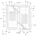
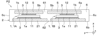
- FIG. 2 is a top layout diagram showing the semiconductor package of the first embodiment. 2 is a sectional view taken along line II-II in FIG. 1.
- FIG. FIG. 3 is an explanatory diagram for explaining a gap between two adjacent bridging members.
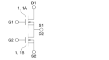
- 1 is a diagram showing a circuit configuration of a semiconductor package according to a first embodiment;
- FIG. FIG. 3 is an explanatory diagram for explaining a semiconductor package of a comparative example and the occurrence of cracks.
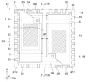
- FIG. 7 is a top layout diagram showing a modification of the semiconductor package of the first embodiment.
- FIG. 7 is a top layout diagram showing a first modified example of the semiconductor package of the second embodiment.
- FIG. 7 is a top layout diagram showing a second modified example of the semiconductor package of the second embodiment.
- FIG. 7 is a top layout diagram showing a semiconductor package of a third embodiment.
- FIG. 7 is a top layout diagram showing a semiconductor package of another embodiment.
- the semiconductor package P1 of the first embodiment will be explained with reference to the drawings.
- the semiconductor package P1 is preferably mounted on a vehicle such as an automobile and used for drive control of various on-vehicle components, but may of course be used for other purposes.
- FIG. 1 the outline of the sealing resin 6, which will be described later, is indicated by a two-dot chain line, the part of the outline of the component covered with the sealing resin 6 that is covered by the bridging member 5, which will be described later, is indicated by a broken line, and the other part is indicated by a solid line. and are shown respectively.
- a second electrode 12 of a semiconductor element 1, which will be described later is hatched.
- the direction along the left-right direction on the page will be referred to as the "x direction”, and the direction perpendicular to the x direction on the same page will be referred to as the "y direction", and the xy plane.
- the normal direction to each is referred to as the "z direction”.
- the x, y, and z directions in the figures after FIG. 2 correspond to the x, y, and z directions in FIG. 1, respectively.
- viewing the semiconductor package P1 from the z direction may be referred to as a "top view.”
- the semiconductor package P1 of this embodiment includes two semiconductor elements 1, a lead frame 2 having a mounting part 21 and a connected part 22, a wire 4, two bridging members 5, A sealing resin 6 covering these is provided.
- the semiconductor package P1 has a 2-in-1 structure in which two semiconductor elements 1 are covered with a sealing resin 6.
- the lead frame 2 is located inside the outer contour of the sealing resin 6, and the surface of the lead frame 2 opposite to the surface on the semiconductor element 1 side is sealed. This is the QFN structure exposed from the stopper resin 6.
- QFN is an abbreviation for Quad Flat Non-leaded package.
- the semiconductor package P1 two semiconductor elements 1 are mounted on different mounting parts 21 arranged independently of each other in a lead frame 2, and these elements are electrically connected via a bridging member 5 and the mounting part 21.
- the circuit configuration is as follows.
- the semiconductor package P1 has, for example, a width of about 8 mm in the x direction, a width of about 7 mm in the y direction, and a thickness of about 0.9 mm in the z direction, but is not limited thereto.
- the semiconductor element 1 for example, a power semiconductor element such as a power MOSFET, an IGBT, or an RC-IGBT in which an IGBT and a diode are integrated can be adopted.
- the semiconductor element 1 is composed of, for example, Si (silicon) or SiC (silicon carbide) as a main component, and is manufactured by a known semiconductor process. Note that in this specification, a case where the semiconductor element 1 is a power MOSFET will be described as a representative example.
- IGBT is an abbreviation for Insulated-Gate Bipolar Transistor.
- the semiconductor element 1 has a rectangular plate shape with its longitudinal direction in the y direction, has a first electrode 11 on one surface 1a on the side of the mounting section 21, and has a first electrode 11 on one surface 1a on the opposite side of the one surface 1a. It has a second electrode 12 and a third electrode 13 on the other side 1b.
- the first electrode 11 is a drain electrode
- the second electrode 12 is a source electrode
- the third electrode 13 is a gate electrode.
- the semiconductor element 1 is mounted on a mounting portion 21 of the lead frame 2 via a bonding material 3 made of a conductive bonding material such as solder, for example.
- first semiconductor element 1A the one located on the left side in the x direction
- second semiconductor element 1A the one located on the right side in the x direction
- semiconductor elements 1A and 1B these may be collectively referred to as “semiconductor elements 1A and 1B,” respectively.
- the surface of the outer surface of the sealing resin 6 that covers the bridging member 5 and is located above the bridging member 5 in the z direction is referred to as an "upper surface 6a”, and is referred to as a surface opposite to the upper surface 6a.
- the side surface will be referred to as a “lower surface 6b,” and the surface connecting the upper surface 6a and the lower surface 6b will be referred to as a "side surface 6c.”
- the semiconductor elements 1A and 1B are each mounted on mounting portions 21 of the lead frame 2 that are arranged apart from each other, and the first electrode 11 and the mounting portion 21 are electrically connected.
- a bridging member 5 is connected to a second electrode 12.
- the first semiconductor element 1A is electrically connected via the bridging member 5 to the mounting section 21 on which the second semiconductor element 1B is mounted.
- the second semiconductor element 1B is electrically connected via the bridging member 5 to a connected part 22 that is arranged apart from the mounting part 21 on which the second semiconductor element 1B is mounted.
- the third electrode 13 is exposed from the bridge member 5, and the wire 4 is connected to the third electrode 13.
- the semiconductor elements 1A and 1B are arranged such that one third electrode 13 is located on the upper side in the y direction and the other third electrode 13 is located on the lower side in the y direction, that is, in a point-symmetrical arrangement. .
- a third electrode 13 is formed near a corner of the other surface 1b facing the other semiconductor element 1.
- the third electrodes 13 of each of the semiconductor elements 1A and 1B are located in a wide area of the gap between two adjacent bridging members 5 when viewed from above.
- the lead frame 2 is made of a metal material such as Cu (copper), Fe (iron), or an alloy thereof, and includes a mounting part 21 on which a semiconductor element is mounted, and a connected part arranged apart from the mounting part 21. 22, and a plurality of terminal portions 23 protruding from the mounting portion 21 or the connected portion 22.
- the lead frame 2 further includes a second terminal portion 24 that is independent from the mounting portion 21 and the connected portion 22, with the terminal portion 23 serving as the first terminal portion 23.
- the mounting portion 21, the connected portion 22, and the second terminal portion 24 are connected by a tie bar (not shown) or the like until the molding of the sealing resin 6, but after the molding of the sealing resin 6. By cutting and removing this connecting part, the parts are finally separated.
- the lead frame 2 includes two mounting parts 21, one connected part 22, and two second terminal parts 24, which are arranged at a distance from each other and are independent of each other.
- the structure is as follows.
- the mounting portion 21 is a portion on which the semiconductor element 1 is mounted.
- the mounting portion 21 includes a plurality of first terminal portions 23 that protrude toward adjacent sides of the sides forming the outer contour of the sealing resin 6 when viewed from above.
- the first terminal portion 23 of the mounting portion 21 is a drain terminal, and is exposed to the outside at the lower surface 6b and side surface 6c of the sealing resin 6.
- one semiconductor element 1 is mounted on each of the two mounting sections 21 .
- first mounting part 21A the one on which the first semiconductor element 1A is mounted among the two mounting parts 21
- second mounting part 21B the one on which the second semiconductor element 1B is mounted
- the lead frame 2 includes a first mounting part 21A on which the first semiconductor element 1A is mounted, a second mounting part 21B on which the second semiconductor element 1B is mounted, and a second mounting part 21B. and a pair of connected parts 22.
- the second mounting portion 21B includes an element mounting portion 211 on which the second semiconductor element 1B is mounted, and an extension portion 212 extending from the element mounting portion 211 to the left side in the x direction.
- the second mounting section 21B is arranged at a distance from the first mounting section 21A and the connected section 22, the element mounting section 211 forms a pair with the connected section 22, and the extending section 212 is arranged at a distance from the first mounting section 21A and the connected section 22. It is paired with the mounting section 21A.
- the bridging member 5 connected to the first semiconductor element 1A is connected to the extension portion 212.
- the connected portion 22 is a member that forms a pair with the mounting portion 21, and similarly to the mounting portion 21, it includes a plurality of first terminal portions 23.
- the connected portion 22 forms a pair with a second mounting portion 21B adjacent in the y direction.
- the connected portion 22 is arranged at a distance from the mounting portion 21, and is connected to one end of the bridging member 5.
- the connected portion 22 is electrically connected to the second electrode 12 of the semiconductor element 1 mounted on the pair of mounting portions 21 via the bridging member 5 .
- the first terminal portion 23 of the connected portion 22 is a source terminal, and is exposed to the outside at the lower surface 6b and side surface 6c of the sealing resin 6.
- the first terminal portion 23 is a plurality of terminals provided on the mounting portion 21 or the connected portion 22, for example, as shown in FIG.
- the first terminal portions 23 are, for example, arranged in parallel with each other with a gap between them.
- the second terminal portion 24 is, for example, a member disposed at a different position from the mounting portion 21 and the connected portion 22 and electrically connected to the third electrode 13 of the semiconductor element 1 via the wire 4.
- the second terminal portion 24 is a gate terminal, and is exposed to the outside at the lower surface 6b and side surface 6c of the sealing resin 6.
- the second terminal portion 24 is partially exposed from the sealing resin 6 and is connected to an external circuit board or the like.
- the second terminal portion 24 has an end gap G2, which will be described later, among the gaps between two adjacent bridging members 5 when viewed from above, that is, from the normal direction to the surface of the mounting portion 21 on which the semiconductor element 1 is mounted. It is arranged near the bridging member 5 so as not to overlap with it.
- the bonding material 3 is made of any conductive bonding material such as solder, and electrically connects each component of the semiconductor package P1.
- the wire 4 is made of a conductive material such as Au (gold), for example.
- the wire 4 is connected to the third electrode 13 and the second terminal portion 24 of the semiconductor element 1 by wire bonding, for example, to electrically connect them.
- the bridging member 5 is, for example, a wide plate-like member whose main component is any conductive material such as a metal material such as Cu, Fe, or an alloy thereof.
- the bridging member 5 is a connecting member that bridges the semiconductor element 1 and a portion of the lead frame 2 and electrically connects them, and may also be referred to as a "clip.”
- the bridging member 5 has a planar size larger than the semiconductor element 1 when viewed from above, and is bonded to the second electrode 12 of the semiconductor element 1 via the bonding material 3. There is.
- the bridging member 5 is disposed, for example, so as to cover the entire other surface 1b of the semiconductor element 1 except for a predetermined region including the third electrode 13 when viewed from above.
- the bridging member 5 covers part or all of the four sides forming the outline of the other surface 1b of the semiconductor element 1, and is arranged to easily diffuse heat during driving of the semiconductor element 1 to the outside.
- all parts of the bridging member 5 other than the connecting parts with the semiconductor element 1 and the lead frame 2 are covered with a sealing resin 6 and are not exposed to the outside. That is, as shown in FIG.
- the bridging member 5 has a surface facing the semiconductor element 1 and the connected portion 22 as a connection surface 5a, and a surface on the opposite side thereof as an opposite surface 5b, and the opposite surface 5b is entirely made of sealing resin. 6, and is insulated from the outside by a sealing resin 6.
- the bridging member 5 is arranged such that the surface of the mounting portion 21 on which the semiconductor element 1 is mounted is the mounting surface, and the height is the dimension in the normal direction to the mounting surface, and the height is the largest compared to other members. ing. In other words, the bridging member 5 is located closest to the upper surface 6a among the members covered with the sealing resin 6. Thereby, the portion of the sealing resin 6 that covers the bridge member 5 can be used as a surface layer, and the thickness of the surface layer can be minimized, and heat dissipation from the bridge member 5 to the outside is advantageous.
- the bridging member 5 connects the semiconductor element 1 located directly below it and a part of the lead frame 2 to which the semiconductor element is connected via itself in the connection direction D1 (in the example of FIG. 1, in the y direction). (along direction), one end in the connection direction D1 is narrower than the center in the same direction.
- the width of the bridging member 5 here is the width in the direction orthogonal to the connection direction D1. Specifically, when viewed from above, the bridging member 5 extends so that one end in the connection direction D1 is away from the adjacent other bridging member 5, and its width is narrower than the center in the same direction. On the other hand, the other end of the bridging member 5 in the connection direction D1 has approximately the same width as the center in the same direction.
- the gap between two adjacent bridging members 5 is such that the gap at the center in the connection direction D1 is defined as the center gap G1, and the gap at the end in the same direction is defined as the end gap G2.
- the relationship is G2.
- the other end of the bridging member 5 connected to the second semiconductor element 1B is bent toward the lead frame 2 side in the connection direction D1, and is connected to the connected portion 22 via the bonding material 3. It is joined.
- the bridging member 5 connected to the first semiconductor element 1A has the same shape as the bridging member 5 described above, is arranged in the opposite direction in the y direction like the semiconductor elements 1A and 1B, and has the other end bent. The side is joined to the second mounting portion 21B via the joining material 3.
- the bridging member 5 is in a so-called hollow state in that portions other than the connecting portions with the semiconductor element 1 and a portion of the lead frame 2 do not come into contact with any member other than the sealing resin 6.
- the sealing resin 6 includes, for example, an electrically insulating resin material such as an epoxy resin, and a filler having a higher thermal conductivity than the resin material.
- the filler for example, inorganic particles such as alumina may be employed.
- the sealing resin 6 is formed, for example, by injection molding using a mold.
- the sealing resin 6 covers the semiconductor element 1 , a part of the lead frame 2 , the bonding material 3 , the wire 4 , and the bridging member 5 .
- the sealing resin 6 has an upper surface 6a and a lower surface 6b that are flat along the xy plane. On the upper surface 6a of the sealing resin 6, other members of the semiconductor package P1 are not exposed, and electrical insulation on the upper surface 6a is ensured.
- the sealing resin 6 preferably has a thermal conductivity of 3 W/m ⁇ K or more, but is not limited thereto.
- a portion of the sealing resin 6 that fills the gap between two adjacent bridging members 5 will be referred to as a "first filling portion 61," as shown in FIG. 1, for example.
- the semiconductor package P1 constitutes a circuit shown in FIG. 4, that is, a circuit in which semiconductor elements 1A and 1B are connected in series via a lead frame 2.
- "D1", “S1”, and “G1” in FIG. 4 correspond to terminals connected to the first electrode 11, second electrode 12, and third electrode 13 of the first semiconductor element 1A, respectively.
- "D2”, “S2”, and “G2” in FIG. 3 correspond to terminals connected to the first electrode 11, second electrode 12, and third electrode 13 of the second semiconductor element 1B, respectively.
- the semiconductor package P1 constitutes a half-bridge circuit in which the first semiconductor element 1A and the second semiconductor element 1B are connected in series, and the terminal portion 23 of the second mounting portion 21B corresponding to the connection portion thereof serves as an output terminal. are doing.
- the terminal portion 23 (D1) of the first mounting portion 21A is connected to an external power source (not shown), and the terminal portion 23 (S2) of the connected portion 22 is connected to a reference potential (GND).
- the first semiconductor element 1A is the high side
- the second semiconductor element 1B is the low side.
- the semiconductor elements 1A and 1B are both N-channel transistors, for example, and the first electrode 11 on one surface 1a is a drain electrode, and the second electrode 12 and third electrode 13 on the other surface 1b are a source electrode and a gate electrode, respectively. It becomes.
- the semiconductor elements 1A and 1B are mounted in a so-called face-up mounting manner, with the other surface 1b on which the second electrode 12 of the source electrode is formed facing the opposite side from the mounting portion 21 functioning as a heat dissipation member.
- the terminal portion 23 of the first mounting portion 21A is the D1 terminal, the power supply terminal, and the terminal portion 24 connected to the third electrode 13 of the first semiconductor element 1A is the G1 terminal, the terminal portion 23 protruding from the extension portion 212. is the S1 terminal.
- the terminal portion 23 of the element mounting portion 211 is the D2 terminal
- the output terminal, the terminal portion 24 connected to the third electrode 13 of the second semiconductor element 1B is the G2 terminal
- the terminal portion 23 of the connected portion 22 is the S2 terminal. It has become.
- a semiconductor package 100 of a comparative example includes two semiconductor elements 1, a lead frame 7 having two pairs of mounting portions 71 and connected portions 72, a bridging member 8, and a sealing resin 6 for sealing these. It has the following.
- the lead frame 7 has a first terminal 73 extending from the mounting part 71 and the connected part 72 to a side of the sealing resin 6 that forms the package outline, and a first terminal 73 extending from the mounting part 71, the connected part 72 and the first terminal 73 It further has an independent second terminal 74.
- the connected part 72 and the mounting part 71 are arranged in order from the upper side in the y direction on the right side in the x direction, and the mounting part 71 and the connected part 72 are arranged in order from the upper side in the y direction on the left side in the x direction. ing.
- a bridge member 8 is connected to the second electrode 12 of each of the semiconductor elements 1C and 1D, and the semiconductor elements 1C and 1D are connected via the bridge member 8 to a connected part 72 that pairs with a mounting part 71 on which the semiconductor elements 1C and 1D are mounted. electrically connected.
- the semiconductor package 100 of the comparative example has a 2-in-1 structure in which the two mounting parts 71 and the connected parts 72 are arranged with a gap between them, and the semiconductor elements 1C and 1D are electrically independent.
- the semiconductor elements 1C and 1D have a third electrode 13 formed on the other surface 1b near the end in the y direction and at the center in the x direction, and the third electrode 13 is exposed from the bridging member 8. ing.
- the third electrode 13 is connected to the wire 4 and is electrically connected to the second terminal 74 .
- the bridging member 8 has a larger planar size than the semiconductor element 1, covers the entire area of the semiconductor element 1 located directly below except for a predetermined area including the third electrode 13, and improves the heat dissipation of the semiconductor element 1. let The bridging member 8 has a shape in which one end located near the third electrode 13 is bifurcated so as to avoid being directly above the third electrode 13.
- the two adjacent bridging members 8 connected to the semiconductor elements 1C and 1D are arranged so that the gap G0 formed between them is substantially constant.
- the gap G0 is set to, for example, about 0.4 mm at the minimum from the viewpoint of ensuring insulation between adjacent bridging members 8 and reducing the size of the entire package.
- the semiconductor package 100 of the comparative example has a structure in which the semiconductor package 100 fills the gap between two adjacent bridging members 8 in the sealing resin 6 during the cooling/heating cycle caused by repeated drive control of the semiconductor element 1. It was found that cracks were generated in the No. 1 filling portion 61.
- the width of the first filling portion 61 is narrow overall, and the end thereof is located near the outer contour of the sealing resin 6. Further, in the semiconductor package 100 of the comparative example, thermal deformation occurs due to the thermal cycle, and stress due to this thermal deformation is concentrated in the first filling portion 61. As a result, in the semiconductor package 100 of the comparative example, heat dissipation can be improved by using the bridging member 8 whose planar size is larger than that of the semiconductor element 1; There is a risk that cracks may occur, resulting in insufficient reliability.
- the width of each of the two adjacent bridging members 5 is narrowed so that one end in the connection direction D1 moves away from the other bridging member 5, and the end gap G2 is The width is wider than the center gap G1.
- the width of the first filling portion 61 in the vicinity of the package outline, where thermal stress due to cooling/heating cycles tends to concentrate is wider than the width in the vicinity of the package center, and the thermal stress is alleviated.
- the semiconductor package P1 is able to efficiently release heat generated by the plurality of semiconductor elements 1 to the outside, and also allows the heat generated by the plurality of semiconductor elements 1 to be efficiently released to the outside. stress is relaxed and crack generation is suppressed.
- the end gap G2 should be at least larger than the center gap G1, but if the center gap G1 is 0.4 mm, it should be made larger than 0.4 mm, preferably twice as large as 0.8 mm.
- a wide bridging member 5 is connected to each of the two semiconductor elements 1, and these are covered with a sealing resin 6, and the gap formed by the adjacent bridging members 5 is a center gap near the center of the package.
- the end gap G2 near the package outer shell is larger than G1.
- the two bridging members 5 are coated with a sealing resin at a portion located closer to the center in the connection direction D1 than the third electrode 13 of the semiconductor element 1 to which they are connected, when viewed from above.
- the shape may include a chamfered portion 51 for relieving the stress of 6.
- each of the two bridging members 5 is formed with a chamfered portion 51 that is a cutout portion that gradually moves away from the other bridging member 5 from near the center of the semiconductor package toward the end.
- the gap in the chamfered part 51 is defined as the chamfer width G3, and the change in width in the direction from the package end toward the package center becomes gentler as G2>G3>G1, and thermal stress caused by the cooling/heating cycle will be further relaxed.
- the inclination and outer shape of the chamfered portion 51 are not limited to the example shown in FIG. 6, and may be changed as appropriate.
- This modification also provides a semiconductor package P1 that provides the same effects as the first embodiment. Furthermore, since the bridging member 5 has the chamfered portion 51, the thermal stress applied to the first filled portion 61 of the sealing resin 6 is further alleviated, and the effect of further suppressing the occurrence of cracks in the sealing resin 6 is also obtained.
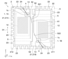
- the portion of the sealing resin 6 that fills the gap between the adjacent mounting portions 21 or connected portions 22 will be referred to as a “second filling portion 62”, as shown in FIG. 7, for example.
- the second filling portion 62 of the sealing resin 6 is located at a position that is not part of the center gap G1 of the first filling portion 61.
- This embodiment differs from the first embodiment in that it has a shifted configuration. In this embodiment, this difference will be mainly explained.
- the two bridging members 5 each have a protruding portion 52 in which a part of the region including the center portion in the connection direction D1 protrudes toward the other bridging member 5.
- the side of the protrusion 52 that faces the other bridging member 5 is inclined with respect to the y direction.
- a portion of the protruding portion 52 extends above the mounting portion 21 on which the semiconductor element 1 is mounted, which is located directly below the opposing bridging member 5 .
- a portion of the protruding portion 52 straddles the gap between the two mounting portions 21 when viewed from above.
- the two bridging members 5 have substantially the same shape and planar size as in the first embodiment.
- the sealing resin 6 is arranged such that a part of the first filling part 61 is shifted from the position of the second filling part 62, as shown in FIG. Specifically, for example, while the second filling part 62 is arranged along one direction (the y direction in the example of FIG. 8), the first filling part 61 is arranged along another direction different from the one direction. It is arranged along a direction (in the example of FIG. 8, a direction other than the y direction), and only a part of it is located on the second filling part 62.
- the thermal stress of the first filling part 61 is relaxed compared to the case where most of the first filling part 61 is located on the second filling part 62, and the first filling part 61 The occurrence of cracks is further suppressed.
- a portion of the first filling portion 61 whose position is shifted from the second filling portion 62 includes both ends in the connection direction D1.
- the first filling portion 61 and the second filling portion 62 are offset” means that the second filling portion 62 This means that the first filling part 61 is shifted in position from the second filling part 62 in a direction that intersects with the first filling part 61 .
- the first filling part 61 is positioned with the second filling part 62 in a direction where a portion thereof intersects with the second filling part 62, that is, in a direction intersecting with the y direction. has been shifted.
- the semiconductor package P2 can obtain the same effects as the first embodiment. Furthermore, since the first filling portion 61 and the second filling portion 62 of the sealing resin 6 are offset, the thermal stress of the second filling portion 62 is difficult to be transmitted to the first filling portion 61, and the sealing resin 6 The effect of further suppressing the occurrence of cracks can also be obtained.
- the semiconductor package P2 has a configuration in which one of the two bridging members 5 protrudes more than the other, so that the first filling part 61 and the second filling part 62 are offset. It may be.
- the semiconductor package P2 is constructed using the first bridge member 5A. Only 5A may have the protrusion 52.
- the first bridging member 5A has, for example, a structure in which the protrusion 52 has a substantially trapezoidal shape when viewed from above, and has a notch 521 in the vicinity of the third electrode 13 of the first semiconductor element 1A directly below.
- the second bridging member 5B does not have the protrusion 52, for example, and has a notch 522 extending away from the first bridging member 5A near the third electrode 13 of the second semiconductor element 1B directly below. It is said that As a result, in addition to shifting the positions of most of the first filling part 61 and the second filling part 62, the sealing resin 6 has notches 521 and 522, which are chamfered parts. The stress in the filling portion 61 is relaxed.
- the width of the portion of the second mounting portion 21B that faces the first mounting portion 21A in the x direction is larger than that of the first mounting portion 21A.
- the first filling part 61 and the second filling part 62 may be offset.
- the width of the connected portion 22 in the x direction is approximately the same as the width in the same direction of the portion of the second mounting portion 21B that faces the first mounting portion 21A in the x direction. In this case, even if the two bridging members 5 have the protruding parts 52 and have substantially the same shape and planar size, the position of the second filling part 62 is x with respect to the first filling part 61 when viewed from above.
- the semiconductor package P2 of the modified example shown in FIG. 10 has a configuration in which the same effects as the modified example shown in FIG. 9 can be obtained.
- This modification also provides a semiconductor package P2 that provides the same effects as the second embodiment.
- one of the two bridging members 5 has a notch 521 and the other has a notch 522, these function as chamfers, further relaxing the stress in the first filling part 61, and cracking the sealing resin 6. The effect of further suppressing the occurrence can also be obtained.
- This embodiment differs from the first embodiment in that it is arranged in the opposite direction. In this embodiment, this difference will be mainly explained.
- the first mounting section 21A replaces a part of the second mounting section 21B and is paired with a connected section 22 that is arranged apart downward in the y direction.
- the second mounting section 21B does not have the extending section 212 that faces the first mounting section 21A in the y direction.
- the lead frame 2 has two pairs of mounting parts 21 and connected parts 22, and the two pairs of mounting parts 21 and connected parts 22 are arranged in parallel in the x direction and facing opposite directions in the y direction. The arrangement is point-symmetrical.
- the first semiconductor element 1A has a bridging member 5 connected to the second electrode 12, and a connected portion that is paired with the first mounting portion 21A of the lead frame 2 via the bridging member 5. 22.
- the first semiconductor element 1A is not electrically connected to the second semiconductor element 1B, and constitutes an independent circuit section.
- the first terminal portion 23 of the first mounting portion 21A, the connected portion 22 paired with the first mounting portion 21A, and the second terminal portion 24 are the drain terminals of the first semiconductor element 1A, respectively. , source terminal, and gate terminal.
- the second semiconductor element 1B is mounted on the second mounting section 21B, and is also mounted on the connected section 22 disposed above the second mounting section 21B in the y direction via the bridging member 5. electrically connected.
- the first terminal portion 23 of the second mounting portion 21B, the connected portion 22 paired with the second mounting portion 21B, and the second terminal portion 24 are the drain terminal, source terminal, and gate of the second semiconductor element 1B, respectively. It is a terminal.
- the semiconductor package P3 has an alternate arrangement in which the arrangement in the y direction of the source terminals and drain terminals in the circuit section on the left side in the x direction is opposite to the arrangement in the y direction of the source terminals and drain terminals in the circuit section on the right side in the x direction. It becomes. Also in this configuration, the two bridging members 5 are shaped such that the end gap G2 in the connection direction D1 is wider than the center gap G1, so that the heat applied to the first filling part 61 of the sealing resin 6 is Stress is relieved.
- This embodiment also provides a semiconductor package P3 that provides the same effects as the first embodiment.
- the semiconductor package has a 2-in-1 structure in which two semiconductor elements 1 are sealed with the sealing resin 6
- the semiconductor package may have an Nin1 structure in which the number of semiconductor elements 1 is N (N ⁇ 3), and in this case, the gap between adjacent bridging members 5 is larger than the center gap G1 by the edge gap G2. If the configuration has a larger value, the effect of suppressing the occurrence of cracks can be obtained.
- the two bridging members 5 have different shapes and planar sizes, and the entire first filling part 61 is replaced by the second filling part 62. It may also be a configuration in which the position is shifted. Moreover, one of the two adjacent bridging members 5 may have a notch 522 in the protruding part 52, and the other may have a structure in which the protruding part 52 does not have a notch.
- the elements constituting the embodiments are not necessarily essential, except in cases where it is specifically specified that they are essential or where they are clearly considered essential in principle. Needless to say.
- numerical values such as the number, numerical value, amount, range, etc. of the constituent elements of the embodiment are mentioned, when it is clearly stated that it is essential, or when it is clearly limited to a specific number in principle. It is not limited to that specific number, except in cases where
- when referring to the shape, positional relationship, etc. of constituent elements, etc., the shape It is not limited to positional relationships, etc.
- a semiconductor package A plurality of semiconductor elements (1), a plurality of plate-shaped bridging members (5) connected to different semiconductor elements; a lead frame (2) having a plurality of mounting portions (21) on which different semiconductor elements are mounted; A sealing resin (6) that covers a portion of the lead frame, the plurality of semiconductor elements, and the bridging member, The plurality of bridging members are arranged at a distance from other bridging members, and the semiconductor element and the mounting part on which the semiconductor element to which it is connected among the lead frames are mounted are separated.
- a direction along the bridging member, which connects the semiconductor element and the different portions, is defined as a connection direction (D1), and a gap between the bridging member and the other adjacent bridging member in the connection direction.
- a semiconductor package, wherein a gap at the center is defined as a center gap (G1), a gap at an end in the connection direction is defined as an end gap (G2), and the end gap is wider than the center gap.
- a first aspect wherein the plurality of bridging members have a larger planar size than the semiconductor element located directly below them, and are arranged so as to cover at least a part of each of four sides forming an outline of the semiconductor element.
- the part of the sealing resin that fills the gap between the adjacent mounting parts is defined as a first filling part (61), and the part that fills the gap between the adjacent bridging members is defined as a second filling part (62).
- the first filling portion is partially or entirely different from the second filling portion in a direction crossing the second filling portion.
- the semiconductor package according to the first or second aspect which is offset.
- the semiconductor element to which the bridging member is connected has a gate electrode (13) on the connection surface (1b) of the bridging member,
- the lead frame has a gate terminal (24) electrically connected to the gate electrode,
- the gate terminal is disposed in the vicinity of the end gap and in a region that does not overlap with the bridging member, when viewed from the normal direction to the surface of the mounting portion on which the semiconductor element is mounted.
Landscapes
- Structures Or Materials For Encapsulating Or Coating Semiconductor Devices Or Solid State Devices (AREA)
- Cooling Or The Like Of Semiconductors Or Solid State Devices (AREA)
Applications Claiming Priority (2)
| Application Number | Priority Date | Filing Date | Title |
|---|---|---|---|
| JP2022142527A JP2024037592A (ja) | 2022-09-07 | 2022-09-07 | 半導体パッケージ |
| JP2022-142527 | 2022-09-07 |
Publications (1)
| Publication Number | Publication Date |
|---|---|
| WO2024053420A1 true WO2024053420A1 (ja) | 2024-03-14 |
Family
ID=90191102
Family Applications (1)
| Application Number | Title | Priority Date | Filing Date |
|---|---|---|---|
| PCT/JP2023/030589 Ceased WO2024053420A1 (ja) | 2022-09-07 | 2023-08-24 | 半導体パッケージ |
Country Status (2)
| Country | Link |
|---|---|
| JP (1) | JP2024037592A (https=) |
| WO (1) | WO2024053420A1 (https=) |
Cited By (1)
| Publication number | Priority date | Publication date | Assignee | Title |
|---|---|---|---|---|
| WO2025205171A1 (ja) * | 2024-03-27 | 2025-10-02 | 株式会社デンソー | 電子装置 |
Citations (4)
| Publication number | Priority date | Publication date | Assignee | Title |
|---|---|---|---|---|
| JP2002100716A (ja) * | 2000-09-21 | 2002-04-05 | Toshiba Corp | 半導体装置の製造方法および半導体装置 |
| DE102019206811A1 (de) * | 2019-05-10 | 2020-11-12 | Robert Bosch Gmbh | Leistungshalbleiterbauelement mit darin angeordneten Leistungstransistoren |
| WO2021005916A1 (ja) * | 2019-07-10 | 2021-01-14 | 株式会社デンソー | 半導体装置及び電子装置 |
| JP2022099720A (ja) * | 2020-12-23 | 2022-07-05 | 株式会社デンソー | 半導体パッケージおよびこれを用いた電子装置 |
-
2022
- 2022-09-07 JP JP2022142527A patent/JP2024037592A/ja active Pending
-
2023
- 2023-08-24 WO PCT/JP2023/030589 patent/WO2024053420A1/ja not_active Ceased
Patent Citations (4)
| Publication number | Priority date | Publication date | Assignee | Title |
|---|---|---|---|---|
| JP2002100716A (ja) * | 2000-09-21 | 2002-04-05 | Toshiba Corp | 半導体装置の製造方法および半導体装置 |
| DE102019206811A1 (de) * | 2019-05-10 | 2020-11-12 | Robert Bosch Gmbh | Leistungshalbleiterbauelement mit darin angeordneten Leistungstransistoren |
| WO2021005916A1 (ja) * | 2019-07-10 | 2021-01-14 | 株式会社デンソー | 半導体装置及び電子装置 |
| JP2022099720A (ja) * | 2020-12-23 | 2022-07-05 | 株式会社デンソー | 半導体パッケージおよびこれを用いた電子装置 |
Cited By (1)
| Publication number | Priority date | Publication date | Assignee | Title |
|---|---|---|---|---|
| WO2025205171A1 (ja) * | 2024-03-27 | 2025-10-02 | 株式会社デンソー | 電子装置 |
Also Published As
| Publication number | Publication date |
|---|---|
| JP2024037592A (ja) | 2024-03-19 |
Similar Documents
| Publication | Publication Date | Title |
|---|---|---|
| JP7331827B2 (ja) | 半導体パッケージおよびこれを用いた電子装置 | |
| US10763240B2 (en) | Semiconductor device comprising signal terminals extending from encapsulant | |
| JP7649171B2 (ja) | 半導体装置 | |
| WO2021005916A1 (ja) | 半導体装置及び電子装置 | |
| JP7845824B2 (ja) | 半導体装置 | |
| KR20190095144A (ko) | 반도체 장치 | |
| JP7473376B2 (ja) | 半導体装置 | |
| CN113228265A (zh) | 半导体组件的电路构造 | |
| JP7594950B2 (ja) | 半導体装置 | |
| WO2024053420A1 (ja) | 半導体パッケージ | |
| WO2023112677A1 (ja) | 半導体装置および半導体装置の製造方法 | |
| JP2021082794A (ja) | 電子部品および電子装置 | |
| JP7630315B2 (ja) | 半導体装置 | |
| JP7396118B2 (ja) | 半導体モジュール | |
| JP7835681B2 (ja) | 半導体装置 | |
| WO2024018790A1 (ja) | 半導体装置 | |
| JP2024108671A (ja) | 半導体製造装置および半導体製造装置の製造方法 | |
| JP2023134143A (ja) | 半導体モジュール、半導体装置、及び車両 | |
| CN101160659A (zh) | 半导体装置及引线框 | |
| JP6812535B2 (ja) | リード端子及び樹脂封止型半導体装置 | |
| JP7681920B2 (ja) | 半導体パッケージ及びその製造方法 | |
| JP7845458B2 (ja) | 金属配線板 | |
| JP7694167B2 (ja) | 半導体装置 | |
| CN110071080A (zh) | 半导体装置及其制造方法 | |
| JP2024061189A (ja) | 半導体モジュール、半導体装置、及び車両 |
Legal Events
| Date | Code | Title | Description |
|---|---|---|---|
| 121 | Ep: the epo has been informed by wipo that ep was designated in this application |
Ref document number: 23862959 Country of ref document: EP Kind code of ref document: A1 |
|
| NENP | Non-entry into the national phase |
Ref country code: DE |
|
| 122 | Ep: pct application non-entry in european phase |
Ref document number: 23862959 Country of ref document: EP Kind code of ref document: A1 |