WO2024053420A1 - 半導体パッケージ - Google Patents
半導体パッケージ Download PDFInfo
- Publication number
- WO2024053420A1 WO2024053420A1 PCT/JP2023/030589 JP2023030589W WO2024053420A1 WO 2024053420 A1 WO2024053420 A1 WO 2024053420A1 JP 2023030589 W JP2023030589 W JP 2023030589W WO 2024053420 A1 WO2024053420 A1 WO 2024053420A1
- Authority
- WO
- WIPO (PCT)
- Prior art keywords
- gap
- semiconductor element
- semiconductor
- mounting
- bridging
- Prior art date
Links
- 239000004065 semiconductor Substances 0.000 title claims abstract description 233
- 229920005989 resin Polymers 0.000 claims abstract description 63
- 239000011347 resin Substances 0.000 claims abstract description 63
- 238000007789 sealing Methods 0.000 claims abstract description 59
- 230000000052 comparative effect Effects 0.000 description 11
- 238000010586 diagram Methods 0.000 description 10
- 230000000694 effects Effects 0.000 description 10
- 239000000463 material Substances 0.000 description 10
- 230000035882 stress Effects 0.000 description 9
- 230000008646 thermal stress Effects 0.000 description 9
- 230000017525 heat dissipation Effects 0.000 description 8
- 230000004048 modification Effects 0.000 description 5
- 238000012986 modification Methods 0.000 description 5
- 238000001816 cooling Methods 0.000 description 4
- 238000010438 heat treatment Methods 0.000 description 4
- XEEYBQQBJWHFJM-UHFFFAOYSA-N iron Substances [Fe] XEEYBQQBJWHFJM-UHFFFAOYSA-N 0.000 description 4
- 239000010949 copper Substances 0.000 description 3
- 229910045601 alloy Inorganic materials 0.000 description 2
- 239000000956 alloy Substances 0.000 description 2
- 239000004020 conductor Substances 0.000 description 2
- 239000000470 constituent Substances 0.000 description 2
- 229910052802 copper Inorganic materials 0.000 description 2
- 239000000945 filler Substances 0.000 description 2
- 239000010931 gold Substances 0.000 description 2
- 229910052742 iron Inorganic materials 0.000 description 2
- 239000007769 metal material Substances 0.000 description 2
- 238000000465 moulding Methods 0.000 description 2
- HBMJWWWQQXIZIP-UHFFFAOYSA-N silicon carbide Chemical compound [Si+]#[C-] HBMJWWWQQXIZIP-UHFFFAOYSA-N 0.000 description 2
- 229910010271 silicon carbide Inorganic materials 0.000 description 2
- 229910000679 solder Inorganic materials 0.000 description 2
- 239000002344 surface layer Substances 0.000 description 2
- RYGMFSIKBFXOCR-UHFFFAOYSA-N Copper Chemical compound [Cu] RYGMFSIKBFXOCR-UHFFFAOYSA-N 0.000 description 1
- PNEYBMLMFCGWSK-UHFFFAOYSA-N aluminium oxide Inorganic materials [O-2].[O-2].[O-2].[Al+3].[Al+3] PNEYBMLMFCGWSK-UHFFFAOYSA-N 0.000 description 1
- 239000012141 concentrate Substances 0.000 description 1
- 238000005336 cracking Methods 0.000 description 1
- 238000010292 electrical insulation Methods 0.000 description 1
- 239000003822 epoxy resin Substances 0.000 description 1
- 230000005669 field effect Effects 0.000 description 1
- -1 for example Substances 0.000 description 1
- PCHJSUWPFVWCPO-UHFFFAOYSA-N gold Chemical compound [Au] PCHJSUWPFVWCPO-UHFFFAOYSA-N 0.000 description 1
- 229910052737 gold Inorganic materials 0.000 description 1
- 238000001746 injection moulding Methods 0.000 description 1
- 239000010954 inorganic particle Substances 0.000 description 1
- 238000009413 insulation Methods 0.000 description 1
- 238000000034 method Methods 0.000 description 1
- 229920000647 polyepoxide Polymers 0.000 description 1
- 230000002040 relaxant effect Effects 0.000 description 1
- 229910052710 silicon Inorganic materials 0.000 description 1
- 239000010703 silicon Substances 0.000 description 1
- 230000001629 suppression Effects 0.000 description 1
Images


Classifications
-
- H—ELECTRICITY
- H01—ELECTRIC ELEMENTS
- H01L—SEMICONDUCTOR DEVICES NOT COVERED BY CLASS H10
- H01L21/00—Processes or apparatus adapted for the manufacture or treatment of semiconductor or solid state devices or of parts thereof
- H01L21/02—Manufacture or treatment of semiconductor devices or of parts thereof
- H01L21/04—Manufacture or treatment of semiconductor devices or of parts thereof the devices having at least one potential-jump barrier or surface barrier, e.g. PN junction, depletion layer or carrier concentration layer
- H01L21/50—Assembly of semiconductor devices using processes or apparatus not provided for in a single one of the subgroups H01L21/06 - H01L21/326, e.g. sealing of a cap to a base of a container
- H01L21/60—Attaching or detaching leads or other conductive members, to be used for carrying current to or from the device in operation
-
- H—ELECTRICITY
- H01—ELECTRIC ELEMENTS
- H01L—SEMICONDUCTOR DEVICES NOT COVERED BY CLASS H10
- H01L23/00—Details of semiconductor or other solid state devices
- H01L23/28—Encapsulations, e.g. encapsulating layers, coatings, e.g. for protection
- H01L23/29—Encapsulations, e.g. encapsulating layers, coatings, e.g. for protection characterised by the material, e.g. carbon
-
- H—ELECTRICITY
- H01—ELECTRIC ELEMENTS
- H01L—SEMICONDUCTOR DEVICES NOT COVERED BY CLASS H10
- H01L23/00—Details of semiconductor or other solid state devices
- H01L23/48—Arrangements for conducting electric current to or from the solid state body in operation, e.g. leads, terminal arrangements ; Selection of materials therefor
-
- H—ELECTRICITY
- H01—ELECTRIC ELEMENTS
- H01L—SEMICONDUCTOR DEVICES NOT COVERED BY CLASS H10
- H01L25/00—Assemblies consisting of a plurality of individual semiconductor or other solid state devices ; Multistep manufacturing processes thereof
- H01L25/03—Assemblies consisting of a plurality of individual semiconductor or other solid state devices ; Multistep manufacturing processes thereof all the devices being of a type provided for in the same subgroup of groups H01L27/00 - H01L33/00, or in a single subclass of H10K, H10N, e.g. assemblies of rectifier diodes
- H01L25/04—Assemblies consisting of a plurality of individual semiconductor or other solid state devices ; Multistep manufacturing processes thereof all the devices being of a type provided for in the same subgroup of groups H01L27/00 - H01L33/00, or in a single subclass of H10K, H10N, e.g. assemblies of rectifier diodes the devices not having separate containers
- H01L25/07—Assemblies consisting of a plurality of individual semiconductor or other solid state devices ; Multistep manufacturing processes thereof all the devices being of a type provided for in the same subgroup of groups H01L27/00 - H01L33/00, or in a single subclass of H10K, H10N, e.g. assemblies of rectifier diodes the devices not having separate containers the devices being of a type provided for in group H01L29/00
-
- H—ELECTRICITY
- H01—ELECTRIC ELEMENTS
- H01L—SEMICONDUCTOR DEVICES NOT COVERED BY CLASS H10
- H01L25/00—Assemblies consisting of a plurality of individual semiconductor or other solid state devices ; Multistep manufacturing processes thereof
- H01L25/18—Assemblies consisting of a plurality of individual semiconductor or other solid state devices ; Multistep manufacturing processes thereof the devices being of types provided for in two or more different subgroups of the same main group of groups H01L27/00 - H01L33/00, or in a single subclass of H10K, H10N
Definitions
- the present disclosure relates to a semiconductor package in which a clip is connected to a semiconductor element.
- a power semiconductor element such as a power MOSFET is mounted on a lead frame, a clip wider than a wire is connected to the power semiconductor element, and the package is sealed with resin.
- MOSFET is an abbreviation for Metal-Oxide-Semiconductor Field-Effect Transistor.
- this type of semiconductor package has a lead frame with two independent islands, a power semiconductor element is mounted on each of the two islands, and these are all sealed together with one resin member.
- a 2-in-1 structure is known.
- the present inventors have conducted extensive studies on semiconductor packages having a structure such as a 2-in-1 structure that has a plurality of power semiconductor elements and in which a wide bridging member such as a clip is bonded to each of the power semiconductor elements. As a result, it has been newly found that in a semiconductor package with this structure, cracks occur in a portion of the sealing resin that fills the gap between two adjacent wide bridge members, which may reduce reliability.
- the present disclosure relates to a semiconductor package that includes a plurality of power semiconductor elements and is capable of ensuring heat dissipation and suppressing cracks in the sealing resin.
- a semiconductor package includes a lead having a plurality of semiconductor elements, a plurality of plate-shaped bridging members connected to different semiconductor elements, and a plurality of mounting parts on which different semiconductor elements are mounted.
- the lead frame is electrically connected to a part of the lead frame that is different from the mounting part on which the semiconductor element to which it is connected is mounted, and the multiple mounting parts are arranged at a distance from other mounting parts.
- connection direction is the direction along the bridging member that connects the semiconductor element to different parts
- the gap between the bridging member and another adjacent bridging member is defined as the gap at the center of the connection direction.
- the gap is defined as a gap
- the gap at the end in the connection direction is defined as an end gap, and the end gap is wider than the center gap.
- the semiconductor package In this semiconductor package, a plurality of semiconductor elements are mounted on different mounting parts of a lead frame, different bridging members are connected to these semiconductor elements, and these members are covered with a sealing resin. Then, the connection direction is the direction along the bridging member and the direction in which the semiconductor element and a part of the lead frame are connected, and the external gap at the end of the connection direction among the gaps between adjacent bridging members is in the same direction. It is wider than the center gap at the center.
- the semiconductor package has a structure in which the sealing resin is filled between adjacent bridging members and does not have a narrow portion near the outer periphery of the package where thermal stress due to drive control of the semiconductor element tends to be concentrated.
- this semiconductor package can radiate heat generated by driving multiple semiconductor elements to the outside via the bridging member of the plate-like member, and can also be used in the sealing resin even after repeated cooling and heating cycles due to drive control of the semiconductor elements. Cracks can be suppressed.
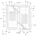
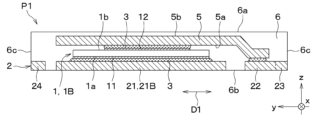
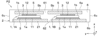
- FIG. 2 is a top layout diagram showing the semiconductor package of the first embodiment. 2 is a sectional view taken along line II-II in FIG. 1.
- FIG. FIG. 3 is an explanatory diagram for explaining a gap between two adjacent bridging members.
- 1 is a diagram showing a circuit configuration of a semiconductor package according to a first embodiment;
- FIG. FIG. 3 is an explanatory diagram for explaining a semiconductor package of a comparative example and the occurrence of cracks.
- FIG. 7 is a top layout diagram showing a modification of the semiconductor package of the first embodiment.
- FIG. 7 is a top layout diagram showing a first modified example of the semiconductor package of the second embodiment.
- FIG. 7 is a top layout diagram showing a second modified example of the semiconductor package of the second embodiment.
- FIG. 7 is a top layout diagram showing a semiconductor package of a third embodiment.
- FIG. 7 is a top layout diagram showing a semiconductor package of another embodiment.
- the semiconductor package P1 of the first embodiment will be explained with reference to the drawings.
- the semiconductor package P1 is preferably mounted on a vehicle such as an automobile and used for drive control of various on-vehicle components, but may of course be used for other purposes.
- FIG. 1 the outline of the sealing resin 6, which will be described later, is indicated by a two-dot chain line, the part of the outline of the component covered with the sealing resin 6 that is covered by the bridging member 5, which will be described later, is indicated by a broken line, and the other part is indicated by a solid line. and are shown respectively.
- a second electrode 12 of a semiconductor element 1, which will be described later is hatched.
- the direction along the left-right direction on the page will be referred to as the "x direction”, and the direction perpendicular to the x direction on the same page will be referred to as the "y direction", and the xy plane.
- the normal direction to each is referred to as the "z direction”.
- the x, y, and z directions in the figures after FIG. 2 correspond to the x, y, and z directions in FIG. 1, respectively.
- viewing the semiconductor package P1 from the z direction may be referred to as a "top view.”
- the semiconductor package P1 of this embodiment includes two semiconductor elements 1, a lead frame 2 having a mounting part 21 and a connected part 22, a wire 4, two bridging members 5, A sealing resin 6 covering these is provided.
- the semiconductor package P1 has a 2-in-1 structure in which two semiconductor elements 1 are covered with a sealing resin 6.
- the lead frame 2 is located inside the outer contour of the sealing resin 6, and the surface of the lead frame 2 opposite to the surface on the semiconductor element 1 side is sealed. This is the QFN structure exposed from the stopper resin 6.
- QFN is an abbreviation for Quad Flat Non-leaded package.
- the semiconductor package P1 two semiconductor elements 1 are mounted on different mounting parts 21 arranged independently of each other in a lead frame 2, and these elements are electrically connected via a bridging member 5 and the mounting part 21.
- the circuit configuration is as follows.
- the semiconductor package P1 has, for example, a width of about 8 mm in the x direction, a width of about 7 mm in the y direction, and a thickness of about 0.9 mm in the z direction, but is not limited thereto.
- the semiconductor element 1 for example, a power semiconductor element such as a power MOSFET, an IGBT, or an RC-IGBT in which an IGBT and a diode are integrated can be adopted.
- the semiconductor element 1 is composed of, for example, Si (silicon) or SiC (silicon carbide) as a main component, and is manufactured by a known semiconductor process. Note that in this specification, a case where the semiconductor element 1 is a power MOSFET will be described as a representative example.
- IGBT is an abbreviation for Insulated-Gate Bipolar Transistor.
- the semiconductor element 1 has a rectangular plate shape with its longitudinal direction in the y direction, has a first electrode 11 on one surface 1a on the side of the mounting section 21, and has a first electrode 11 on one surface 1a on the opposite side of the one surface 1a. It has a second electrode 12 and a third electrode 13 on the other side 1b.
- the first electrode 11 is a drain electrode
- the second electrode 12 is a source electrode
- the third electrode 13 is a gate electrode.
- the semiconductor element 1 is mounted on a mounting portion 21 of the lead frame 2 via a bonding material 3 made of a conductive bonding material such as solder, for example.
- first semiconductor element 1A the one located on the left side in the x direction
- second semiconductor element 1A the one located on the right side in the x direction
- semiconductor elements 1A and 1B these may be collectively referred to as “semiconductor elements 1A and 1B,” respectively.
- the surface of the outer surface of the sealing resin 6 that covers the bridging member 5 and is located above the bridging member 5 in the z direction is referred to as an "upper surface 6a”, and is referred to as a surface opposite to the upper surface 6a.
- the side surface will be referred to as a “lower surface 6b,” and the surface connecting the upper surface 6a and the lower surface 6b will be referred to as a "side surface 6c.”
- the semiconductor elements 1A and 1B are each mounted on mounting portions 21 of the lead frame 2 that are arranged apart from each other, and the first electrode 11 and the mounting portion 21 are electrically connected.
- a bridging member 5 is connected to a second electrode 12.
- the first semiconductor element 1A is electrically connected via the bridging member 5 to the mounting section 21 on which the second semiconductor element 1B is mounted.
- the second semiconductor element 1B is electrically connected via the bridging member 5 to a connected part 22 that is arranged apart from the mounting part 21 on which the second semiconductor element 1B is mounted.
- the third electrode 13 is exposed from the bridge member 5, and the wire 4 is connected to the third electrode 13.
- the semiconductor elements 1A and 1B are arranged such that one third electrode 13 is located on the upper side in the y direction and the other third electrode 13 is located on the lower side in the y direction, that is, in a point-symmetrical arrangement. .
- a third electrode 13 is formed near a corner of the other surface 1b facing the other semiconductor element 1.
- the third electrodes 13 of each of the semiconductor elements 1A and 1B are located in a wide area of the gap between two adjacent bridging members 5 when viewed from above.
- the lead frame 2 is made of a metal material such as Cu (copper), Fe (iron), or an alloy thereof, and includes a mounting part 21 on which a semiconductor element is mounted, and a connected part arranged apart from the mounting part 21. 22, and a plurality of terminal portions 23 protruding from the mounting portion 21 or the connected portion 22.
- the lead frame 2 further includes a second terminal portion 24 that is independent from the mounting portion 21 and the connected portion 22, with the terminal portion 23 serving as the first terminal portion 23.
- the mounting portion 21, the connected portion 22, and the second terminal portion 24 are connected by a tie bar (not shown) or the like until the molding of the sealing resin 6, but after the molding of the sealing resin 6. By cutting and removing this connecting part, the parts are finally separated.
- the lead frame 2 includes two mounting parts 21, one connected part 22, and two second terminal parts 24, which are arranged at a distance from each other and are independent of each other.
- the structure is as follows.
- the mounting portion 21 is a portion on which the semiconductor element 1 is mounted.
- the mounting portion 21 includes a plurality of first terminal portions 23 that protrude toward adjacent sides of the sides forming the outer contour of the sealing resin 6 when viewed from above.
- the first terminal portion 23 of the mounting portion 21 is a drain terminal, and is exposed to the outside at the lower surface 6b and side surface 6c of the sealing resin 6.
- one semiconductor element 1 is mounted on each of the two mounting sections 21 .
- first mounting part 21A the one on which the first semiconductor element 1A is mounted among the two mounting parts 21
- second mounting part 21B the one on which the second semiconductor element 1B is mounted
- the lead frame 2 includes a first mounting part 21A on which the first semiconductor element 1A is mounted, a second mounting part 21B on which the second semiconductor element 1B is mounted, and a second mounting part 21B. and a pair of connected parts 22.
- the second mounting portion 21B includes an element mounting portion 211 on which the second semiconductor element 1B is mounted, and an extension portion 212 extending from the element mounting portion 211 to the left side in the x direction.
- the second mounting section 21B is arranged at a distance from the first mounting section 21A and the connected section 22, the element mounting section 211 forms a pair with the connected section 22, and the extending section 212 is arranged at a distance from the first mounting section 21A and the connected section 22. It is paired with the mounting section 21A.
- the bridging member 5 connected to the first semiconductor element 1A is connected to the extension portion 212.
- the connected portion 22 is a member that forms a pair with the mounting portion 21, and similarly to the mounting portion 21, it includes a plurality of first terminal portions 23.
- the connected portion 22 forms a pair with a second mounting portion 21B adjacent in the y direction.
- the connected portion 22 is arranged at a distance from the mounting portion 21, and is connected to one end of the bridging member 5.
- the connected portion 22 is electrically connected to the second electrode 12 of the semiconductor element 1 mounted on the pair of mounting portions 21 via the bridging member 5 .
- the first terminal portion 23 of the connected portion 22 is a source terminal, and is exposed to the outside at the lower surface 6b and side surface 6c of the sealing resin 6.
- the first terminal portion 23 is a plurality of terminals provided on the mounting portion 21 or the connected portion 22, for example, as shown in FIG.
- the first terminal portions 23 are, for example, arranged in parallel with each other with a gap between them.
- the second terminal portion 24 is, for example, a member disposed at a different position from the mounting portion 21 and the connected portion 22 and electrically connected to the third electrode 13 of the semiconductor element 1 via the wire 4.
- the second terminal portion 24 is a gate terminal, and is exposed to the outside at the lower surface 6b and side surface 6c of the sealing resin 6.
- the second terminal portion 24 is partially exposed from the sealing resin 6 and is connected to an external circuit board or the like.
- the second terminal portion 24 has an end gap G2, which will be described later, among the gaps between two adjacent bridging members 5 when viewed from above, that is, from the normal direction to the surface of the mounting portion 21 on which the semiconductor element 1 is mounted. It is arranged near the bridging member 5 so as not to overlap with it.
- the bonding material 3 is made of any conductive bonding material such as solder, and electrically connects each component of the semiconductor package P1.
- the wire 4 is made of a conductive material such as Au (gold), for example.
- the wire 4 is connected to the third electrode 13 and the second terminal portion 24 of the semiconductor element 1 by wire bonding, for example, to electrically connect them.
- the bridging member 5 is, for example, a wide plate-like member whose main component is any conductive material such as a metal material such as Cu, Fe, or an alloy thereof.
- the bridging member 5 is a connecting member that bridges the semiconductor element 1 and a portion of the lead frame 2 and electrically connects them, and may also be referred to as a "clip.”
- the bridging member 5 has a planar size larger than the semiconductor element 1 when viewed from above, and is bonded to the second electrode 12 of the semiconductor element 1 via the bonding material 3. There is.
- the bridging member 5 is disposed, for example, so as to cover the entire other surface 1b of the semiconductor element 1 except for a predetermined region including the third electrode 13 when viewed from above.
- the bridging member 5 covers part or all of the four sides forming the outline of the other surface 1b of the semiconductor element 1, and is arranged to easily diffuse heat during driving of the semiconductor element 1 to the outside.
- all parts of the bridging member 5 other than the connecting parts with the semiconductor element 1 and the lead frame 2 are covered with a sealing resin 6 and are not exposed to the outside. That is, as shown in FIG.
- the bridging member 5 has a surface facing the semiconductor element 1 and the connected portion 22 as a connection surface 5a, and a surface on the opposite side thereof as an opposite surface 5b, and the opposite surface 5b is entirely made of sealing resin. 6, and is insulated from the outside by a sealing resin 6.
- the bridging member 5 is arranged such that the surface of the mounting portion 21 on which the semiconductor element 1 is mounted is the mounting surface, and the height is the dimension in the normal direction to the mounting surface, and the height is the largest compared to other members. ing. In other words, the bridging member 5 is located closest to the upper surface 6a among the members covered with the sealing resin 6. Thereby, the portion of the sealing resin 6 that covers the bridge member 5 can be used as a surface layer, and the thickness of the surface layer can be minimized, and heat dissipation from the bridge member 5 to the outside is advantageous.
- the bridging member 5 connects the semiconductor element 1 located directly below it and a part of the lead frame 2 to which the semiconductor element is connected via itself in the connection direction D1 (in the example of FIG. 1, in the y direction). (along direction), one end in the connection direction D1 is narrower than the center in the same direction.
- the width of the bridging member 5 here is the width in the direction orthogonal to the connection direction D1. Specifically, when viewed from above, the bridging member 5 extends so that one end in the connection direction D1 is away from the adjacent other bridging member 5, and its width is narrower than the center in the same direction. On the other hand, the other end of the bridging member 5 in the connection direction D1 has approximately the same width as the center in the same direction.
- the gap between two adjacent bridging members 5 is such that the gap at the center in the connection direction D1 is defined as the center gap G1, and the gap at the end in the same direction is defined as the end gap G2.
- the relationship is G2.
- the other end of the bridging member 5 connected to the second semiconductor element 1B is bent toward the lead frame 2 side in the connection direction D1, and is connected to the connected portion 22 via the bonding material 3. It is joined.
- the bridging member 5 connected to the first semiconductor element 1A has the same shape as the bridging member 5 described above, is arranged in the opposite direction in the y direction like the semiconductor elements 1A and 1B, and has the other end bent. The side is joined to the second mounting portion 21B via the joining material 3.
- the bridging member 5 is in a so-called hollow state in that portions other than the connecting portions with the semiconductor element 1 and a portion of the lead frame 2 do not come into contact with any member other than the sealing resin 6.
- the sealing resin 6 includes, for example, an electrically insulating resin material such as an epoxy resin, and a filler having a higher thermal conductivity than the resin material.
- the filler for example, inorganic particles such as alumina may be employed.
- the sealing resin 6 is formed, for example, by injection molding using a mold.
- the sealing resin 6 covers the semiconductor element 1 , a part of the lead frame 2 , the bonding material 3 , the wire 4 , and the bridging member 5 .
- the sealing resin 6 has an upper surface 6a and a lower surface 6b that are flat along the xy plane. On the upper surface 6a of the sealing resin 6, other members of the semiconductor package P1 are not exposed, and electrical insulation on the upper surface 6a is ensured.
- the sealing resin 6 preferably has a thermal conductivity of 3 W/m ⁇ K or more, but is not limited thereto.
- a portion of the sealing resin 6 that fills the gap between two adjacent bridging members 5 will be referred to as a "first filling portion 61," as shown in FIG. 1, for example.
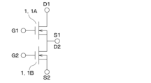
- the semiconductor package P1 constitutes a circuit shown in FIG. 4, that is, a circuit in which semiconductor elements 1A and 1B are connected in series via a lead frame 2.
- "D1", “S1”, and “G1” in FIG. 4 correspond to terminals connected to the first electrode 11, second electrode 12, and third electrode 13 of the first semiconductor element 1A, respectively.
- "D2”, “S2”, and “G2” in FIG. 3 correspond to terminals connected to the first electrode 11, second electrode 12, and third electrode 13 of the second semiconductor element 1B, respectively.
- the semiconductor package P1 constitutes a half-bridge circuit in which the first semiconductor element 1A and the second semiconductor element 1B are connected in series, and the terminal portion 23 of the second mounting portion 21B corresponding to the connection portion thereof serves as an output terminal. are doing.
- the terminal portion 23 (D1) of the first mounting portion 21A is connected to an external power source (not shown), and the terminal portion 23 (S2) of the connected portion 22 is connected to a reference potential (GND).
- the first semiconductor element 1A is the high side
- the second semiconductor element 1B is the low side.
- the semiconductor elements 1A and 1B are both N-channel transistors, for example, and the first electrode 11 on one surface 1a is a drain electrode, and the second electrode 12 and third electrode 13 on the other surface 1b are a source electrode and a gate electrode, respectively. It becomes.
- the semiconductor elements 1A and 1B are mounted in a so-called face-up mounting manner, with the other surface 1b on which the second electrode 12 of the source electrode is formed facing the opposite side from the mounting portion 21 functioning as a heat dissipation member.
- the terminal portion 23 of the first mounting portion 21A is the D1 terminal, the power supply terminal, and the terminal portion 24 connected to the third electrode 13 of the first semiconductor element 1A is the G1 terminal, the terminal portion 23 protruding from the extension portion 212. is the S1 terminal.
- the terminal portion 23 of the element mounting portion 211 is the D2 terminal
- the output terminal, the terminal portion 24 connected to the third electrode 13 of the second semiconductor element 1B is the G2 terminal
- the terminal portion 23 of the connected portion 22 is the S2 terminal. It has become.
- a semiconductor package 100 of a comparative example includes two semiconductor elements 1, a lead frame 7 having two pairs of mounting portions 71 and connected portions 72, a bridging member 8, and a sealing resin 6 for sealing these. It has the following.
- the lead frame 7 has a first terminal 73 extending from the mounting part 71 and the connected part 72 to a side of the sealing resin 6 that forms the package outline, and a first terminal 73 extending from the mounting part 71, the connected part 72 and the first terminal 73 It further has an independent second terminal 74.
- the connected part 72 and the mounting part 71 are arranged in order from the upper side in the y direction on the right side in the x direction, and the mounting part 71 and the connected part 72 are arranged in order from the upper side in the y direction on the left side in the x direction. ing.
- a bridge member 8 is connected to the second electrode 12 of each of the semiconductor elements 1C and 1D, and the semiconductor elements 1C and 1D are connected via the bridge member 8 to a connected part 72 that pairs with a mounting part 71 on which the semiconductor elements 1C and 1D are mounted. electrically connected.
- the semiconductor package 100 of the comparative example has a 2-in-1 structure in which the two mounting parts 71 and the connected parts 72 are arranged with a gap between them, and the semiconductor elements 1C and 1D are electrically independent.
- the semiconductor elements 1C and 1D have a third electrode 13 formed on the other surface 1b near the end in the y direction and at the center in the x direction, and the third electrode 13 is exposed from the bridging member 8. ing.
- the third electrode 13 is connected to the wire 4 and is electrically connected to the second terminal 74 .
- the bridging member 8 has a larger planar size than the semiconductor element 1, covers the entire area of the semiconductor element 1 located directly below except for a predetermined area including the third electrode 13, and improves the heat dissipation of the semiconductor element 1. let The bridging member 8 has a shape in which one end located near the third electrode 13 is bifurcated so as to avoid being directly above the third electrode 13.
- the two adjacent bridging members 8 connected to the semiconductor elements 1C and 1D are arranged so that the gap G0 formed between them is substantially constant.
- the gap G0 is set to, for example, about 0.4 mm at the minimum from the viewpoint of ensuring insulation between adjacent bridging members 8 and reducing the size of the entire package.
- the semiconductor package 100 of the comparative example has a structure in which the semiconductor package 100 fills the gap between two adjacent bridging members 8 in the sealing resin 6 during the cooling/heating cycle caused by repeated drive control of the semiconductor element 1. It was found that cracks were generated in the No. 1 filling portion 61.
- the width of the first filling portion 61 is narrow overall, and the end thereof is located near the outer contour of the sealing resin 6. Further, in the semiconductor package 100 of the comparative example, thermal deformation occurs due to the thermal cycle, and stress due to this thermal deformation is concentrated in the first filling portion 61. As a result, in the semiconductor package 100 of the comparative example, heat dissipation can be improved by using the bridging member 8 whose planar size is larger than that of the semiconductor element 1; There is a risk that cracks may occur, resulting in insufficient reliability.
- the width of each of the two adjacent bridging members 5 is narrowed so that one end in the connection direction D1 moves away from the other bridging member 5, and the end gap G2 is The width is wider than the center gap G1.
- the width of the first filling portion 61 in the vicinity of the package outline, where thermal stress due to cooling/heating cycles tends to concentrate is wider than the width in the vicinity of the package center, and the thermal stress is alleviated.
- the semiconductor package P1 is able to efficiently release heat generated by the plurality of semiconductor elements 1 to the outside, and also allows the heat generated by the plurality of semiconductor elements 1 to be efficiently released to the outside. stress is relaxed and crack generation is suppressed.
- the end gap G2 should be at least larger than the center gap G1, but if the center gap G1 is 0.4 mm, it should be made larger than 0.4 mm, preferably twice as large as 0.8 mm.
- a wide bridging member 5 is connected to each of the two semiconductor elements 1, and these are covered with a sealing resin 6, and the gap formed by the adjacent bridging members 5 is a center gap near the center of the package.
- the end gap G2 near the package outer shell is larger than G1.
- the two bridging members 5 are coated with a sealing resin at a portion located closer to the center in the connection direction D1 than the third electrode 13 of the semiconductor element 1 to which they are connected, when viewed from above.
- the shape may include a chamfered portion 51 for relieving the stress of 6.
- each of the two bridging members 5 is formed with a chamfered portion 51 that is a cutout portion that gradually moves away from the other bridging member 5 from near the center of the semiconductor package toward the end.
- the gap in the chamfered part 51 is defined as the chamfer width G3, and the change in width in the direction from the package end toward the package center becomes gentler as G2>G3>G1, and thermal stress caused by the cooling/heating cycle will be further relaxed.
- the inclination and outer shape of the chamfered portion 51 are not limited to the example shown in FIG. 6, and may be changed as appropriate.
- This modification also provides a semiconductor package P1 that provides the same effects as the first embodiment. Furthermore, since the bridging member 5 has the chamfered portion 51, the thermal stress applied to the first filled portion 61 of the sealing resin 6 is further alleviated, and the effect of further suppressing the occurrence of cracks in the sealing resin 6 is also obtained.
- the portion of the sealing resin 6 that fills the gap between the adjacent mounting portions 21 or connected portions 22 will be referred to as a “second filling portion 62”, as shown in FIG. 7, for example.
- the second filling portion 62 of the sealing resin 6 is located at a position that is not part of the center gap G1 of the first filling portion 61.
- This embodiment differs from the first embodiment in that it has a shifted configuration. In this embodiment, this difference will be mainly explained.
- the two bridging members 5 each have a protruding portion 52 in which a part of the region including the center portion in the connection direction D1 protrudes toward the other bridging member 5.
- the side of the protrusion 52 that faces the other bridging member 5 is inclined with respect to the y direction.
- a portion of the protruding portion 52 extends above the mounting portion 21 on which the semiconductor element 1 is mounted, which is located directly below the opposing bridging member 5 .
- a portion of the protruding portion 52 straddles the gap between the two mounting portions 21 when viewed from above.
- the two bridging members 5 have substantially the same shape and planar size as in the first embodiment.
- the sealing resin 6 is arranged such that a part of the first filling part 61 is shifted from the position of the second filling part 62, as shown in FIG. Specifically, for example, while the second filling part 62 is arranged along one direction (the y direction in the example of FIG. 8), the first filling part 61 is arranged along another direction different from the one direction. It is arranged along a direction (in the example of FIG. 8, a direction other than the y direction), and only a part of it is located on the second filling part 62.
- the thermal stress of the first filling part 61 is relaxed compared to the case where most of the first filling part 61 is located on the second filling part 62, and the first filling part 61 The occurrence of cracks is further suppressed.
- a portion of the first filling portion 61 whose position is shifted from the second filling portion 62 includes both ends in the connection direction D1.
- the first filling portion 61 and the second filling portion 62 are offset” means that the second filling portion 62 This means that the first filling part 61 is shifted in position from the second filling part 62 in a direction that intersects with the first filling part 61 .
- the first filling part 61 is positioned with the second filling part 62 in a direction where a portion thereof intersects with the second filling part 62, that is, in a direction intersecting with the y direction. has been shifted.
- the semiconductor package P2 can obtain the same effects as the first embodiment. Furthermore, since the first filling portion 61 and the second filling portion 62 of the sealing resin 6 are offset, the thermal stress of the second filling portion 62 is difficult to be transmitted to the first filling portion 61, and the sealing resin 6 The effect of further suppressing the occurrence of cracks can also be obtained.
- the semiconductor package P2 has a configuration in which one of the two bridging members 5 protrudes more than the other, so that the first filling part 61 and the second filling part 62 are offset. It may be.
- the semiconductor package P2 is constructed using the first bridge member 5A. Only 5A may have the protrusion 52.
- the first bridging member 5A has, for example, a structure in which the protrusion 52 has a substantially trapezoidal shape when viewed from above, and has a notch 521 in the vicinity of the third electrode 13 of the first semiconductor element 1A directly below.
- the second bridging member 5B does not have the protrusion 52, for example, and has a notch 522 extending away from the first bridging member 5A near the third electrode 13 of the second semiconductor element 1B directly below. It is said that As a result, in addition to shifting the positions of most of the first filling part 61 and the second filling part 62, the sealing resin 6 has notches 521 and 522, which are chamfered parts. The stress in the filling portion 61 is relaxed.
- the width of the portion of the second mounting portion 21B that faces the first mounting portion 21A in the x direction is larger than that of the first mounting portion 21A.
- the first filling part 61 and the second filling part 62 may be offset.
- the width of the connected portion 22 in the x direction is approximately the same as the width in the same direction of the portion of the second mounting portion 21B that faces the first mounting portion 21A in the x direction. In this case, even if the two bridging members 5 have the protruding parts 52 and have substantially the same shape and planar size, the position of the second filling part 62 is x with respect to the first filling part 61 when viewed from above.
- the semiconductor package P2 of the modified example shown in FIG. 10 has a configuration in which the same effects as the modified example shown in FIG. 9 can be obtained.
- This modification also provides a semiconductor package P2 that provides the same effects as the second embodiment.
- one of the two bridging members 5 has a notch 521 and the other has a notch 522, these function as chamfers, further relaxing the stress in the first filling part 61, and cracking the sealing resin 6. The effect of further suppressing the occurrence can also be obtained.
- This embodiment differs from the first embodiment in that it is arranged in the opposite direction. In this embodiment, this difference will be mainly explained.
- the first mounting section 21A replaces a part of the second mounting section 21B and is paired with a connected section 22 that is arranged apart downward in the y direction.
- the second mounting section 21B does not have the extending section 212 that faces the first mounting section 21A in the y direction.
- the lead frame 2 has two pairs of mounting parts 21 and connected parts 22, and the two pairs of mounting parts 21 and connected parts 22 are arranged in parallel in the x direction and facing opposite directions in the y direction. The arrangement is point-symmetrical.
- the first semiconductor element 1A has a bridging member 5 connected to the second electrode 12, and a connected portion that is paired with the first mounting portion 21A of the lead frame 2 via the bridging member 5. 22.
- the first semiconductor element 1A is not electrically connected to the second semiconductor element 1B, and constitutes an independent circuit section.
- the first terminal portion 23 of the first mounting portion 21A, the connected portion 22 paired with the first mounting portion 21A, and the second terminal portion 24 are the drain terminals of the first semiconductor element 1A, respectively. , source terminal, and gate terminal.
- the second semiconductor element 1B is mounted on the second mounting section 21B, and is also mounted on the connected section 22 disposed above the second mounting section 21B in the y direction via the bridging member 5. electrically connected.
- the first terminal portion 23 of the second mounting portion 21B, the connected portion 22 paired with the second mounting portion 21B, and the second terminal portion 24 are the drain terminal, source terminal, and gate of the second semiconductor element 1B, respectively. It is a terminal.
- the semiconductor package P3 has an alternate arrangement in which the arrangement in the y direction of the source terminals and drain terminals in the circuit section on the left side in the x direction is opposite to the arrangement in the y direction of the source terminals and drain terminals in the circuit section on the right side in the x direction. It becomes. Also in this configuration, the two bridging members 5 are shaped such that the end gap G2 in the connection direction D1 is wider than the center gap G1, so that the heat applied to the first filling part 61 of the sealing resin 6 is Stress is relieved.
- This embodiment also provides a semiconductor package P3 that provides the same effects as the first embodiment.
- the semiconductor package has a 2-in-1 structure in which two semiconductor elements 1 are sealed with the sealing resin 6
- the semiconductor package may have an Nin1 structure in which the number of semiconductor elements 1 is N (N ⁇ 3), and in this case, the gap between adjacent bridging members 5 is larger than the center gap G1 by the edge gap G2. If the configuration has a larger value, the effect of suppressing the occurrence of cracks can be obtained.
- the two bridging members 5 have different shapes and planar sizes, and the entire first filling part 61 is replaced by the second filling part 62. It may also be a configuration in which the position is shifted. Moreover, one of the two adjacent bridging members 5 may have a notch 522 in the protruding part 52, and the other may have a structure in which the protruding part 52 does not have a notch.
- the elements constituting the embodiments are not necessarily essential, except in cases where it is specifically specified that they are essential or where they are clearly considered essential in principle. Needless to say.
- numerical values such as the number, numerical value, amount, range, etc. of the constituent elements of the embodiment are mentioned, when it is clearly stated that it is essential, or when it is clearly limited to a specific number in principle. It is not limited to that specific number, except in cases where
- when referring to the shape, positional relationship, etc. of constituent elements, etc., the shape It is not limited to positional relationships, etc.
- a semiconductor package A plurality of semiconductor elements (1), a plurality of plate-shaped bridging members (5) connected to different semiconductor elements; a lead frame (2) having a plurality of mounting portions (21) on which different semiconductor elements are mounted; A sealing resin (6) that covers a portion of the lead frame, the plurality of semiconductor elements, and the bridging member, The plurality of bridging members are arranged at a distance from other bridging members, and the semiconductor element and the mounting part on which the semiconductor element to which it is connected among the lead frames are mounted are separated.
- a direction along the bridging member, which connects the semiconductor element and the different portions, is defined as a connection direction (D1), and a gap between the bridging member and the other adjacent bridging member in the connection direction.
- a semiconductor package, wherein a gap at the center is defined as a center gap (G1), a gap at an end in the connection direction is defined as an end gap (G2), and the end gap is wider than the center gap.
- a first aspect wherein the plurality of bridging members have a larger planar size than the semiconductor element located directly below them, and are arranged so as to cover at least a part of each of four sides forming an outline of the semiconductor element.
- the part of the sealing resin that fills the gap between the adjacent mounting parts is defined as a first filling part (61), and the part that fills the gap between the adjacent bridging members is defined as a second filling part (62).
- the first filling portion is partially or entirely different from the second filling portion in a direction crossing the second filling portion.
- the semiconductor package according to the first or second aspect which is offset.
- the semiconductor element to which the bridging member is connected has a gate electrode (13) on the connection surface (1b) of the bridging member,
- the lead frame has a gate terminal (24) electrically connected to the gate electrode,
- the gate terminal is disposed in the vicinity of the end gap and in a region that does not overlap with the bridging member, when viewed from the normal direction to the surface of the mounting portion on which the semiconductor element is mounted.
Abstract
半導体パッケージは、複数の半導体素子(1)と、異なる半導体素子に接続される複数の板状の架橋部材(5)と、異なる半導体素子が搭載される複数の実装部(21)を有するリードフレーム(2)と、リードフレームの一部、複数の半導体素子および架橋部材を覆う封止樹脂(6)とを備える。複数の架橋部材は、他の架橋部材とは距離を隔てて配置され、半導体素子と、リードフレームのうち自身が接続された半導体素子が搭載された実装部とは異なる部位(21、22)と、を電気的に接続している。複数の実装部は、他の実装部とは距離を隔てて配置される。架橋部材に沿った方向であって、半導体素子と上記異なる部位とを繋ぐ方向を接続方向(D1)とし、架橋部材と隣接する他の架橋部材との隙間のうち接続方向の中心における隙間を中心隙間(G1)とし、接続方向の端部における隙間を端部隙間(G2)として、端部隙間は、中心隙間よりも幅が広い。
Description
本出願は、2022年9月7日に出願された日本特許出願番号2022-142527号に基づくもので、ここにその記載内容が参照により組み入れられる。
本開示は、半導体素子にクリップが接続された半導体パッケージに関する。
従来、例えば特許文献1に記載の半導体パッケージのように、リードフレーム上にパワーMOSFET等のパワー半導体素子が搭載され、パワー半導体素子にワイヤよりも幅広のクリップが接続されると共に、樹脂封止された構造が知られている。なお、MOSFETとは、Metal-Oxide-Semiconductor Field-Effect Transistorの略称である。また、この種の半導体パッケージとしては、リードフレームが独立した2つのアイランドを有し、2つのアイランドそれぞれにパワー半導体素子が搭載され、これらがまとめて1つの樹脂部材により封止されてなる、いわゆる2in1構造が知られている。
駆動時の発熱量が大きい複数のパワー半導体素子を用いた半導体パッケージは、放熱性向上の観点から、それぞれの半導体素子に接続するクリップの面積をできる限り大きくすることが好ましい。
2in1構造のように複数のパワー半導体素子を有し、パワー半導体素子のそれぞれにクリップ等の幅広の架橋部材を接合した構造の半導体パッケージについて本発明者らが鋭意検討を行った。その結果、当該構造の半導体パッケージでは、封止樹脂のうち2つの隣接する幅広の架橋部材の隙間を充填する部位にクラックが生じ、信頼性が低下しうることが新たに判明した。
本開示は、複数のパワー半導体素子を有し、放熱性確保と封止樹脂のクラック抑制とを両立可能な半導体パッケージに関する。
本開示の1つの観点によれば、半導体パッケージは、複数の半導体素子と、異なる半導体素子に接続される複数の板状の架橋部材と、異なる半導体素子が搭載される複数の実装部を有するリードフレームと、リードフレームの一部、複数の半導体素子および架橋部材を覆う封止樹脂と、を備え、複数の架橋部材は、他の架橋部材とは距離を隔てて配置されると共に、半導体素子と、リードフレームのうち自身が接続された半導体素子が搭載された実装部とは異なる部位と、を電気的に接続しており、複数の実装部は、他の実装部とは距離を隔てて配置されており、架橋部材に沿った方向であって、半導体素子と異なる部位とを繋ぐ方向を接続方向とし、架橋部材と隣接する他の架橋部材との隙間のうち接続方向の中心における隙間を中心隙間とし、接続方向の端部における隙間を端部隙間として、端部隙間は、中心隙間よりも幅が広い。
この半導体パッケージは、複数の半導体素子がリードフレームのうち異なる実装部にそれぞれ搭載され、これらの半導体素子には異なる架橋部材が接続され、これらの部材が封止樹脂に覆われている。そして、架橋部材に沿った方向であって、半導体素子とリードフレームの一部とを繋ぐ方向を接続方向として、隣接する架橋部材の隙間のうち接続方向の端部における外部隙間は、同方向の中心における中心隙間よりも幅が広くなっている。つまり、半導体パッケージは、封止樹脂による隣接する架橋部材間の充填部分であって、半導体素子の駆動制御による熱応力が集中しやすい狭幅部位をパッケージの外郭近傍に有しない構成となる。これにより、この半導体パッケージは、板状部材の架橋部材を介して複数の半導体素子の駆動による熱を外部に放熱しつつも、半導体素子の駆動制御による冷熱サイクルを繰り返しても封止樹脂でのクラック発生を抑制することができる。
なお、各構成要素等に付された括弧付きの参照符号は、その構成要素等と後述する実施形態に記載の具体的な構成要素等との対応関係の一例を示すものである。
以下、本開示の実施形態について図に基づいて説明する。なお、以下の各実施形態相互において、互いに同一もしくは均等である部分には、同一符号を付して説明を行う。
(第1実施形態)
第1実施形態の半導体パッケージP1について、図面を参照して説明する。半導体パッケージP1は、例えば、自動車等の車両に搭載され、各種車載部品の駆動制御に用いられると好適であるが、勿論、他の用途にも採用されうる。
第1実施形態の半導体パッケージP1について、図面を参照して説明する。半導体パッケージP1は、例えば、自動車等の車両に搭載され、各種車載部品の駆動制御に用いられると好適であるが、勿論、他の用途にも採用されうる。
図1では、後述する封止樹脂6の外郭を二点鎖線で、封止樹脂6に覆われた構成部材の外郭のうち後述する架橋部材5に覆われる部分を破線で、その他の部分を実線で、それぞれ示している。また、図1では、見易くするため、断面を示すものではないが、後述する半導体素子1の第2電極12にハッチングを施している。これらの点は、後述する図3、5~7、9~12についても同様である。
以下、説明の便宜上、図1に示すように、紙面上の左右方向に沿った方向を「x方向」と、同紙面上においてx方向に対して垂直な方向を「y方向」と、xy平面に対する法線方向を「z方向」と、それぞれ称する。図2以降の図におけるx、y、zの各方向は、それぞれ図1中のx、y、zの各方向に対応するものである。また、図1に示すように、半導体パッケージP1をz方向から見ることを「上面視」と称することがある。
〔半導体パッケージ〕
本実施形態の半導体パッケージP1は、例えば図1に示すように、2つの半導体素子1と、実装部21および被接続部22を有するリードフレーム2と、ワイヤ4と、2つの架橋部材5と、これらを覆う封止樹脂6とを備える。半導体パッケージP1は、2つの半導体素子1が封止樹脂6に覆われた2in1構造である。また、半導体パッケージP1は、例えば図1や図2に示すように、リードフレーム2が封止樹脂6の外郭内側に位置し、リードフレーム2のうち半導体素子1側の面とは反対面が封止樹脂6から露出したQFN構造である。QFNとは、Quad Flat Non-leaded packageの略称である。半導体パッケージP1は、2つの半導体素子1がそれぞれリードフレーム2のうち互いに独立して配置された異なる実装部21に搭載され、これらの素子が架橋部材5および実装部21を介して電気的に接続された回路構成となっている。半導体パッケージP1は、例えば、x方向における幅が8mm程度、y方向における幅が7mm程度、z方向における厚みが0.9mm程度のサイズとされるが、これに限定されない。
本実施形態の半導体パッケージP1は、例えば図1に示すように、2つの半導体素子1と、実装部21および被接続部22を有するリードフレーム2と、ワイヤ4と、2つの架橋部材5と、これらを覆う封止樹脂6とを備える。半導体パッケージP1は、2つの半導体素子1が封止樹脂6に覆われた2in1構造である。また、半導体パッケージP1は、例えば図1や図2に示すように、リードフレーム2が封止樹脂6の外郭内側に位置し、リードフレーム2のうち半導体素子1側の面とは反対面が封止樹脂6から露出したQFN構造である。QFNとは、Quad Flat Non-leaded packageの略称である。半導体パッケージP1は、2つの半導体素子1がそれぞれリードフレーム2のうち互いに独立して配置された異なる実装部21に搭載され、これらの素子が架橋部材5および実装部21を介して電気的に接続された回路構成となっている。半導体パッケージP1は、例えば、x方向における幅が8mm程度、y方向における幅が7mm程度、z方向における厚みが0.9mm程度のサイズとされるが、これに限定されない。
半導体素子1としては、例えば、パワーMOSFET、IGBTやIGBTとダイオードとを一体化したRC-IGBT等のパワー半導体素子が採用されうる。半導体素子1は、例えば、Si(シリコン)やSiC(炭化珪素)を主成分として構成され、公知の半導体プロセスにより製造される。なお、本明細書では、半導体素子1がパワーMOSFETである場合を代表例として説明する。また、IGBTとは、Insulated‐Gate Bipolar Transistorの略称である。
例えば、半導体素子1は、図1や図2に示すように、y方向を長手方向とする矩形板状とされ、実装部21側の一面1aに第1電極11を有し、一面1aの反対側の他面1bに第2電極12および第3電極13を有してなる。半導体素子1は、第1電極11がドレイン電極、第2電極12がソース電極、第3電極13がゲート電極となっている。半導体素子1は、例えば、はんだ等の導電性接合材料によりなる接合材3を介して、リードフレーム2のうち実装部21に搭載されている。
以下、説明の便宜上、図1に示すように、2つの半導体素子1のうちx方向左側に位置するものを「第1半導体素子1A」と、x方向右側に位置するものを「第2半導体素子1B」と、これらを総称して「半導体素子1A、1B」と、それぞれ称することがある。また、同様に、図2に示すように、封止樹脂6の外表面のうち架橋部材5を覆い、架橋部材5よりもz方向上側に位置する面を「上面6a」と、上面6aの反対側の面を「下面6b」と、上面6aと下面6bとを繋ぐ面を「側面6c」と、それぞれ称する。
半導体素子1A、1Bは、それぞれ、リードフレーム2のうち互いに離れて配置された実装部21に搭載され、第1電極11と実装部21とが電気的に接続されている。半導体素子1A、1Bは、それぞれ、第2電極12に架橋部材5が接続されている。第1半導体素子1Aは、架橋部材5を介して、第2半導体素子1Bが搭載された実装部21と電気的に接続されている。第2半導体素子1Bは、架橋部材5を介して、自身が搭載されている実装部21から離れて配置された被接続部22と電気的に接続されている。半導体素子1A、1Bは、それぞれ、第3電極13が架橋部材5から露出すると共に、第3電極13にワイヤ4が接続されている。半導体素子1A、1Bは、例えば、上面視にて、一方の第3電極13がy方向上側、他方の第3電極13がy方向下側に位置する配置、すなわち点対象の配置とされている。半導体素子1A、1Bは、他面1bのうち他の半導体素子1と向き合う角部近傍に第3電極13が形成されている。言い換えると、半導体素子1A、1Bそれぞれの第3電極13は、上面視にて、2つの隣接する架橋部材5のなす隙間のうち広い領域に位置している。
リードフレーム2は、例えば、Cu(銅)、Fe(鉄)やその合金等の金属材料によりなり、半導体素子が搭載される実装部21と、実装部21から離間して配置される被接続部22と、実装部21または被接続部22から突出する複数の端子部23とを有する。リードフレーム2は、さらに、端子部23を第1の端子部23として、実装部21および被接続部22から独立した第2の端子部24を有する。リードフレーム2は、例えば、封止樹脂6の成型までは、実装部21、被接続部22および第2の端子部24が図示しないタイバー等により連結されているが、封止樹脂6の成型後にこの連結部分が切断除去されることで最終的に分離した状態とされている。リードフレーム2は、本実施形態では、2つの実装部21と、1つの被接続部22と、2つの第2の端子部24とを備え、これらが互いに距離を隔てて配置され、互いに独立した構成となっている。
実装部21は、半導体素子1が搭載される部位である。実装部21は、例えば図1に示すように、上面視にて、封止樹脂6の外郭をなす辺のうち近接する辺に向かって突出する複数の第1の端子部23を備える。実装部21の第1の端子部23は、本実施形態では、ドレイン端子となっており、封止樹脂6の下面6bおよび側面6cにおいて外部に露出している。2つの実装部21は、例えば、それぞれ半導体素子1が1つずつ搭載されている。
以下、説明の便宜上、2つの実装部21のうち第1半導体素子1Aが搭載されるものを「第1の実装部21A」と、第2半導体素子1Bが搭載されるものを「第2の実装部21B」と、それぞれ称することがある。
リードフレーム2は、本実施形態では、第1半導体素子1Aが搭載される第1の実装部21Aと、第2半導体素子1Bが搭載される第2の実装部21Bと、第2の実装部21Bと対をなす被接続部22とによりなる。
第2の実装部21Bは、第2半導体素子1Bが搭載される素子搭載部211と、素子搭載部211からx方向左側に延設された延設部212とを有してなる。第2の実装部21Bは、第1の実装部21Aおよび被接続部22から距離を隔てて配置されると共に、素子搭載部211が被接続部22と対をなし、延設部212が第1の実装部21Aと対をなしている。第2の実装部21Bは、第1半導体素子1Aに接続された架橋部材5が延設部212に接続されている。
被接続部22は、実装部21と対をなす部材であり、実装部21と同様に複数の第1の端子部23を備える。被接続部22は、例えば、y方向において隣接する第2の実装部21Bと対をなしている。被接続部22は、例えば図1や図2に示すように、実装部21とは距離を隔てて配置され、架橋部材5の一端が接続されている。被接続部22は、対をなす実装部21上に搭載された半導体素子1の第2電極12と架橋部材5を介して電気的に接続されている。被接続部22の第1の端子部23は、本実施形態では、ソース端子となっており、封止樹脂6の下面6bおよび側面6cにおいて外部に露出している。
第1の端子部23は、例えば図1に示すように、実装部21または被接続部22に複数設けられる端子である。第1の端子部23は、例えば、互いに隙間を隔てて平行配置される。
第2の端子部24は、例えば、実装部21および被接続部22とは異なる位置に配置され、ワイヤ4を介して半導体素子1の第3電極13に電気的に接続される部材である。第2の端子部24は、本実施形態では、ゲート端子となっており、封止樹脂6の下面6bおよび側面6cにおいて外部に露出している。第2の端子部24は、例えば図2に示すように、一部が封止樹脂6から露出しており、外部の回路基板等に接続される。第2の端子部24は、上面視、すなわち実装部21のうち半導体素子1が搭載される面に対する法線方向から見て、隣接する2つの架橋部材5の隙間のうち後述する端部隙間G2の近傍に、架橋部材5とは重畳しないように配置されている。
接合材3は、例えば、はんだ等の任意の導電性接合材料により構成され、半導体パッケージP1の各構成要素を電気的に接続する。
ワイヤ4は、例えば、Au(金)等の導電性材料により構成される。ワイヤ4は、例えば、ワイヤボンディングにより半導体素子1の第3電極13および第2の端子部24に接続され、これらを電気的に接続している。
架橋部材5としては、例えば、Cu、Feやその合金等の金属材料といった任意の導電性材料を主成分とした幅広の板状部材である。架橋部材5は、半導体素子1とリードフレーム2の一部とを架橋し、これらを電気的に接続する接続部材であり、「クリップ」とも称されうる。架橋部材5は、例えば、図1や図3に示すように、上面視にて、半導体素子1よりも平面サイズが大きく、接合材3を介して半導体素子1の第2電極12に接合されている。
架橋部材5は、例えば、上面視にて、半導体素子1の他面1bのうち第3電極13を含む所定領域を除く他の領域をすべて覆うように配置される。言い換えると、架橋部材5は、半導体素子1の他面1bの外郭をなす四辺の一部または全部を覆っており、半導体素子1の駆動時の熱を外部に拡散しやすい配置となっている。架橋部材5は、例えば、半導体素子1およびリードフレーム2との接続部分以外の部分が、すべて封止樹脂6により覆われており、外部に露出しない状態となっている。すなわち、架橋部材5は、図2に示すように、半導体素子1および被接続部22側の面を接続面5aとし、その反対側の面を反対面5bとして、反対面5bがすべて封止樹脂6に覆われており、封止樹脂6により外部と絶縁されている。
架橋部材5は、実装部21のうち半導体素子1が搭載される面を実装面とし、実装面に対する法線方向における寸法を高さとして、高さが他の部材に比べて最も大きい配置とされている。言い換えると、架橋部材5は、封止樹脂6に覆われる部材の中で最も上面6aに近い配置となっている。これにより、封止樹脂6のうち架橋部材5を覆う部分を表層部として、表層部の厚みを最小限とすることができ、架橋部材5から外部への放熱が有利となる。
架橋部材5は、自身の直下に位置する半導体素子1と自身を介して当該半導体素子が接続されるリードフレーム2の一部とを繋ぐ方向を接続方向D1(図1の例では、y方向に沿った方向)として、接続方向D1の一端が同方向の中心よりも幅が狭くなっている。ここでいう架橋部材5の幅とは、接続方向D1に対して直交する方向における幅である。具体的には、架橋部材5は、上面視にて、接続方向D1の一端が隣接する他の架橋部材5から遠ざかるように延設され、その幅が同方向の中心よりも狭くなっている。その一方で、架橋部材5のうち接続方向D1の他端側は、同方向の中心と略同一の幅となっている。その結果、隣接する2つの架橋部材5の隙間は、例えば図3に示すように、接続方向D1における中心の隙間を中心隙間G1とし、同方向の端部における隙間を端部隙間G2として、G1<G2の関係となっている。これにより、封止樹脂6のうち隣接する2つの架橋部材5の隙間を充填する部分における応力が緩和され、クラック発生が抑制される。この詳細については後述する。
第2半導体素子1Bに接続された架橋部材5は、図2に示すように、接続方向D1の他端側がリードフレーム2側に向かって折り曲げられると共に、接合材3を介して被接続部22に接合されている。第1半導体素子1Aに接続された架橋部材5は、上記した架橋部材5と同様の形状であると共に、半導体素子1A、1Bと同様にy方向において逆向きの配置とされ、折り曲げられた他端側が接合材3を介して第2の実装部21Bに接合されている。架橋部材5は、半導体素子1およびリードフレーム2の一部との接続部分以外の部分が、封止樹脂6以外の部材とは接触しない、いわば中空の状態となっている。
封止樹脂6は、例えば、エポキシ樹脂等といった電気絶縁性の樹脂材料と、当該樹脂材料よりも熱伝導率が大きいフィラーとを有してなる。フィラーとしては、例えば、アルミナ等の無機物粒子が採用されうる。封止樹脂6は、例えば、金型を用いた射出成型等の方法により形成される。封止樹脂6は、半導体素子1、リードフレーム2の一部、接合材3、ワイヤ4および架橋部材5を覆っている。封止樹脂6は、例えば、上面6aおよび下面6bがxy平面に沿った平坦面とされる。封止樹脂6の上面6aにおいては、半導体パッケージP1の他の部材が露出しない状態となっており、上面6aにおける電気絶縁性が確保されている。封止樹脂6は、高い放熱性を実現する観点から、熱伝導率が3W/m・K以上とされることが好ましいが、これに限定されない。以下、説明の便宜上、例えば図1に示すように、封止樹脂6のうち隣接する2つの架橋部材5の隙間を充填する部分を「第1充填部61」と称する。
以上が、本実施形態の半導体パッケージP1の基本的な構成である。
〔回路構成例〕
半導体パッケージP1は、例えば、本実施形態では、図4に示す回路、すなわち半導体素子1A、1Bがリードフレーム2を介して直列接続された回路を構成している。図4における「D1」、「S1」、「G1」は、それぞれ、第1半導体素子1Aの第1電極11、第2電極12、第3電極13に接続された端子に相当する。図3における「D2」、「S2」、「G2」は、それぞれ、第2半導体素子1Bの第1電極11、第2電極12、第3電極13に接続された端子に相当する。
半導体パッケージP1は、例えば、本実施形態では、図4に示す回路、すなわち半導体素子1A、1Bがリードフレーム2を介して直列接続された回路を構成している。図4における「D1」、「S1」、「G1」は、それぞれ、第1半導体素子1Aの第1電極11、第2電極12、第3電極13に接続された端子に相当する。図3における「D2」、「S2」、「G2」は、それぞれ、第2半導体素子1Bの第1電極11、第2電極12、第3電極13に接続された端子に相当する。
半導体パッケージP1は、第1半導体素子1Aと第2半導体素子1Bとが直列接続され、これらの結線部分に相当する第2の実装部21Bの端子部23が出力端子となる、ハーフブリッジ回路を構成している。半導体パッケージP1は、例えば、第1の実装部21Aの端子部23(D1)が図示しない外部電源に接続され、被接続部22の端子部23(S2)が基準電位(GND)に接続される。例えば、第1半導体素子1Aがハイサイド、第2半導体素子1Bがローサイドである。半導体素子1A、1Bは、例えば、いずれもNチャネル型のトランジスタとされ、一面1aの第1電極11がドレイン電極、他面1bの第2電極12、第3電極13がそれぞれソース電極、ゲート電極となっている。半導体素子1A、1Bは、ソース電極の第2電極12が形成された他面1bを、放熱部材として機能する実装部21とは反対側に向けた搭載形態、いわゆるフェイスアップ実装となっている。
つまり、第1の実装部21Aの端子部23がD1端子、電源端子、第1半導体素子1Aの第3電極13に接続された端子部24がG1端子、延設部212から突出する端子部23がS1端子となっている。また、素子搭載部211の端子部23がD2端子、出力端子、第2半導体素子1Bの第3電極13に接続された端子部24がG2端子、被接続部22の端子部23がS2端子となっている。
〔封止樹脂のクラック抑制〕
次に、隣接する2つの架橋部材5が、端部隙間G2>中心隙間G1となる形状および配置とされることによる効果について、図5に示す比較例の半導体パッケージ100と対比して説明する。
次に、隣接する2つの架橋部材5が、端部隙間G2>中心隙間G1となる形状および配置とされることによる効果について、図5に示す比較例の半導体パッケージ100と対比して説明する。
まず、比較例の半導体パッケージ100について説明する。
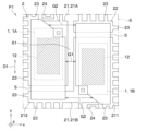
比較例の半導体パッケージ100は、2つの半導体素子1と、対をなす実装部71および被接続部72を二対有したリードフレーム7と、架橋部材8と、これらを封止する封止樹脂6とを有してなる。リードフレーム7は、実装部71および被接続部72から封止樹脂6のうちパッケージ外郭をなす辺に延設された第1端子73と、実装部71、被接続部72および第1端子73から独立した第2端子74とをさらに有する。比較例の半導体パッケージ100は、x方向右側ではy方向上側から順に被接続部72、実装部71が配置され、x方向左側ではy方向上側から順に実装部71、被接続部72、が配置されている。比較例の半導体パッケージ100は、半導体素子1C、1Dがそれぞれの第2電極12に架橋部材8が接続され、自身が搭載された実装部71と対をなす被接続部72に架橋部材8を介して電気的に接続されている。比較例の半導体パッケージ100は、2つの実装部71および被接続部72が互いに隙間を隔てて配置されており、半導体素子1C、1Dが電気的に独立した構成の2in1構造である。
半導体素子1C、1Dは、図5に示すように、他面1bのうちy方向における端部近傍かつx方向における中心に第3電極13が形成され、第3電極13が架橋部材8から露出している。第3電極13は、ワイヤ4が接続され、第2端子74と電気的に接続されている。架橋部材8は、半導体素子1よりも平面サイズが大きく、直下に位置する半導体素子1のうち第3電極13を含む所定の領域を除く全領域を覆っており、半導体素子1の放熱性を向上させる。架橋部材8は、第3電極13の近傍に位置する一端が第3電極13の真上を避けるように二股に枝分かれした形状となっている。半導体素子1C、1Dに接続された2つの隣接する架橋部材8は、これらのなす隙間G0が略一定となる配置になっている。なお、隙間G0は、例えば、隣接する架橋部材8間の絶縁性確保およびパッケージ全体の小型化の両立の観点から、最小で0.4mm程度とされる。
本発明者らの鋭意検討の結果、比較例の半導体パッケージ100は、半導体素子1の駆動制御の繰り返しによる冷熱サイクルにおいて、封止樹脂6のうち2つの隣接する架橋部材8の隙間を充填する第1充填部61にクラックが生じることが判明した。
具体的には、比較例の半導体パッケージ100は、第1充填部61の幅が全体的に狭く、かつその端部が封止樹脂6の外郭近傍に位置している。また、比較例の半導体パッケージ100は、冷熱サイクルにより熱変形が生じ、この熱変形に伴う応力が第1充填部61に集中してしまう。その結果、比較例の半導体パッケージ100は、半導体素子1よりも平面サイズが大きい架橋部材8を用いることで放熱性を向上できるが、第1充填部61の端部を起点とした封止樹脂6のクラックが生じてしまうおそれがあり、信頼性確保が不十分となりうる。
これに対して、本実施形態の半導体パッケージP1は、隣接する2つの架橋部材5がそれぞれ接続方向D1の一端が他の架橋部材5から遠ざかるように幅が狭くなっており、端部隙間G2が中心隙間G1よりも幅が広くなっている。これにより、第1充填部61は、冷熱サイクルに伴う熱応力が集中しやすいパッケージ外郭近傍における幅がパッケージ中心近傍の幅よりも広く、熱応力が緩和される。その結果、半導体パッケージP1は、複数の幅広の架橋部材5を用いることで複数の半導体素子1に起因する熱を効率良く外部に逃がすことができると共に、封止樹脂6の第1充填部61への応力が緩和され、クラック発生が抑制される。なお、例えば、端部隙間G2は、少なくとも中心隙間G1よりも大きければよいが、中心隙間G1が0.4mmである場合には、0.4mmよりも大きくされ、好ましくは2倍の0.8mm以上とされるが、これに限定されない。
本実施形態の半導体パッケージP1は、2つの半導体素子1それぞれに幅広の架橋部材5が接続され、これらが封止樹脂6に覆われ、隣接する架橋部材5のなす隙間がパッケージ中心近傍の中心隙間G1よりもパッケージ外郭近傍の端部隙間G2のほうが大きい。これにより、半導体素子1の駆動による熱を平面サイズが半導体素子1よりも大きい架橋部材5により広範囲に放出できると共に、第1充填部61の端部の幅が中心部位よりも広く、端部の応力が緩和される。そのため、半導体パッケージP1は、放熱性確保およびクラック抑制を両立することができる。
(第1実施形態の変形例)
2つの架橋部材5は、例えば図6に示すように、上面視にて、自身が接続される半導体素子1の第3電極13よりも接続方向D1の中心側に位置する部位に、封止樹脂6の応力を緩和するための面取り部51が形成された形状であってもよい。具体的には、2つの架橋部材5は、それぞれ、半導体パッケージ中心近傍から端部に向かうにつれて徐々に他方の架橋部材5から遠ざかる切り欠き部位とされた面取り部51が形成されている。これにより、第1充填部61は、面取り部51における隙間を面取り幅G3として、パッケージ端部からパッケージ中心に向かう方向における幅の変化がG2>G3>G1とより緩やかとなり、冷熱サイクルによる熱応力がさらに緩和される。なお、面取り部51の傾斜や外形については、図6に示す例に限定されるものではなく、適宜変更されうる。
2つの架橋部材5は、例えば図6に示すように、上面視にて、自身が接続される半導体素子1の第3電極13よりも接続方向D1の中心側に位置する部位に、封止樹脂6の応力を緩和するための面取り部51が形成された形状であってもよい。具体的には、2つの架橋部材5は、それぞれ、半導体パッケージ中心近傍から端部に向かうにつれて徐々に他方の架橋部材5から遠ざかる切り欠き部位とされた面取り部51が形成されている。これにより、第1充填部61は、面取り部51における隙間を面取り幅G3として、パッケージ端部からパッケージ中心に向かう方向における幅の変化がG2>G3>G1とより緩やかとなり、冷熱サイクルによる熱応力がさらに緩和される。なお、面取り部51の傾斜や外形については、図6に示す例に限定されるものではなく、適宜変更されうる。
本変形例によっても、上記第1実施形態と同様の効果が得られる半導体パッケージP1となる。また、架橋部材5が面取り部51を有することにより、封止樹脂6の第1充填部61にかかる熱応力がさらに緩和され、封止樹脂6のクラック発生をより抑制できる効果も得られる。
(第2実施形態)
第2実施形態の半導体パッケージP2について、図面を参照して説明する。
第2実施形態の半導体パッケージP2について、図面を参照して説明する。
以下、説明の便宜上、例えば図7に示すように、封止樹脂6のうち隣接する実装部21または被接続部22の隙間を充填する部分を「第2充填部62」と称する。
本実施形態の半導体パッケージP2は、例えば図7や図8に示すように、封止樹脂6のうち第2充填部62が、第1充填部61のうち中心隙間G1の一部とは位置がずれた構成となっている点で上記第1実施形態と相違する。本実施形態では、この相違点について主に説明する。
2つの架橋部材5は、本実施形態では、接続方向D1における中心部分を含む一部の領域が他方の架橋部材5に向かって突き出した突出部52を有する。突出部52は、例えば、他方の架橋部材5と向き合う辺がy方向に対して傾いている。突出部52の一部は、対向する架橋部材5の直下に位置する半導体素子1が搭載された実装部21上まで延設されている。言い換えると、突出部52は、上面視にて、一部が2つの実装部21の隙間を跨いでいる。なお、2つの架橋部材5は、上記第1実施形態と同様に、略同一の形状および平面サイズとされる。
封止樹脂6は、本実施形態では、図8に示すように、第1充填部61の一部が第2充填部62とは位置をずらされた配置となっている。具体的には、例えば、第2充填部62がある一方向(図8の例ではy方向)に沿った配置であるのに対し、第1充填部61は、当該一方向とは異なる他の方向(図8の例ではy方向以外の方向)に沿った配置とされ、一部のみが第2充填部62上に位置している。これにより、封止樹脂6は、半導体素子1の駆動制御に伴う熱応力が第2充填部62にかかった場合であっても、第1充填部61の大部分が第2充填部62とオフセットされているため、当該熱応力が第1充填部61に伝わりづらい構成となる。したがって、封止樹脂6は、第1充填部61の大部分が第2充填部62上に位置している場合に比べて、第1充填部61の熱応力が緩和され、第1充填部61でのクラック発生がより抑制される。なお、第1充填部61のうち第2充填部62と位置がずらされる部位は、応力緩和の観点から、接続方向D1における両端を含むことが好ましい。また、「第1充填部61と第2充填部62とがオフセットされている」とは、実装部21のうち半導体素子1が搭載される面に対する法線方向から見て、第2充填部62に対して交差する方向に第1充填部61が第2充填部62と位置がずらされていることをいう。例えば図7に示すように、第1充填部61は、上面視にて、一部が第2充填部62に対して交差する方向、すなわちy方向と交差する方向において第2充填部62と位置がずらされている。
本実施形態によれば、上記第1実施形態と同様の効果が得られる半導体パッケージP2となる。また、封止樹脂6の第1充填部61と第2充填部62とがオフセットされていることで、第2充填部62の熱応力が第1充填部61に伝わりづらくなり、封止樹脂6のクラック発生をより抑制できる効果も得られる。
(第2実施形態の変形例)
半導体パッケージP2は、例えば図9に示すように、2つの架橋部材5の一方が他方よりも突出した構成とされることで、第1充填部61と第2充填部62とがオフセットされた構成であってもよい。例えば、2つの架橋部材5のうち第1半導体素子1Aに直接接続されるものを「第1架橋部材5A」とし、他方を「第2架橋部材5B」として、半導体パッケージP2は、第1架橋部材5Aのみが突出部52を有する構成とされうる。また、第1架橋部材5Aは、例えば、突出部52が上面視にて略台形状とされ、直下の第1半導体素子1Aの第3電極13の近傍に切欠部521を有した構成とされる。一方、第2架橋部材5Bは、例えば、突出部52を有しておらず、直下の第2半導体素子1Bの第3電極13の近傍に第1架橋部材5Aから遠ざかる切欠部522を有した構成とされる。これにより、封止樹脂6は、第1充填部61の大部分と第2充填部62との位置がずらされることに加えて、面取り部である切欠部521、522を有することにより、第1充填部61の応力が緩和される。
半導体パッケージP2は、例えば図9に示すように、2つの架橋部材5の一方が他方よりも突出した構成とされることで、第1充填部61と第2充填部62とがオフセットされた構成であってもよい。例えば、2つの架橋部材5のうち第1半導体素子1Aに直接接続されるものを「第1架橋部材5A」とし、他方を「第2架橋部材5B」として、半導体パッケージP2は、第1架橋部材5Aのみが突出部52を有する構成とされうる。また、第1架橋部材5Aは、例えば、突出部52が上面視にて略台形状とされ、直下の第1半導体素子1Aの第3電極13の近傍に切欠部521を有した構成とされる。一方、第2架橋部材5Bは、例えば、突出部52を有しておらず、直下の第2半導体素子1Bの第3電極13の近傍に第1架橋部材5Aから遠ざかる切欠部522を有した構成とされる。これにより、封止樹脂6は、第1充填部61の大部分と第2充填部62との位置がずらされることに加えて、面取り部である切欠部521、522を有することにより、第1充填部61の応力が緩和される。
半導体パッケージP2は、例えば図10に示すように、第2の実装部21Bのうちx方向にて第1の実装部21Aと対向する部分のx方向における幅が第1の実装部21Aよりも大きく、第1充填部61と第2充填部62とがオフセットされた構成であってもよい。また、被接続部22は、x方向における幅が、第2の実装部21Bのうちx方向において第1の実装部21Aと対向する部分の同方向における幅と略同一とされる。この場合、2つの架橋部材5が突出部52を有し、略同一の形状および平面サイズであっても、上面視にて、第2充填部62の位置が第1充填部61に対してx方向左側にずれるため、第1充填部61と第2充填部62とがオフセットされる。そのため、図10に示す変形例の半導体パッケージP2は、図9に示す変形例と同様の効果が得られる構成となっている。
本変形例によっても、上記第2実施形態と同様の効果が得られる半導体パッケージP2となる。また、2つの架橋部材5の一方が切欠部521、他方が切欠部522を有することで、これらが面取り部として機能し、第1充填部61の応力をさらに緩和し、封止樹脂6のクラック発生をより抑制できる効果も得られる。
(第3実施形態)
第3実施形態の半導体パッケージP3について、図面を参照して説明する。
第3実施形態の半導体パッケージP3について、図面を参照して説明する。
本実施形態の半導体パッケージP3は、例えば図11に示すように、リードフレーム2が2つの実装部21および2つの被接続部22を有し、二対の実装部21および被接続部22がy方向において逆向きに配置された構成である点で上記第1実施形態と相違する。本実施形態では、この相違点について主に説明する。
リードフレーム2は、本実施形態では、第1の実装部21Aが第2の実装部21Bの一部に代わって、y方向下側に離れて配置された被接続部22と対をなしている。第2の実装部21Bは、本実施形態では、第1の実装部21Aとy方向において第1の実装部21Aと対向する延設部212を有していない。リードフレーム2は、対をなす実装部21および被接続部22を2つ有してなり、二対の実装部21および被接続部22がx方向において平行配置、かつy方向において逆方向を向く配置、すなわち点対称の配置とされている。
第1半導体素子1Aは、本実施形態では、第2電極12に架橋部材5が接続されると共に、架橋部材5を介してリードフレーム2のうち第1の実装部21Aと対をなす被接続部22に電気的に接続されている。第1半導体素子1Aは、第2半導体素子1Bとは電気的に接続されておらず、独立した回路部を構成している。本実施形態では、第1の実装部21Aの第1の端子部23、第1の実装部21Aと対をなす被接続部22、第2の端子部24がそれぞれ第1半導体素子1Aのドレイン端子、ソース端子、ゲート端子となっている。
第2半導体素子1Bは、本実施形態では、第2の実装部21Bに搭載されると共に、架橋部材5を介して第2の実装部21Bよりもy方向上側に配置された被接続部22に電気的に接続されている。第2の実装部21Bの第1の端子部23、第2の実装部21Bと対をなす被接続部22、第2の端子部24がそれぞれ第2半導体素子1Bのドレイン端子、ソース端子、ゲート端子となっている。
つまり、半導体パッケージP3は、x方向左側の回路部におけるソース端子およびドレイン端子のy方向における配置と、x方向右側の回路部におけるソース端子およびドレイン端子のy方向における配置とが逆である交互配置となっている。この構成においても2つの架橋部材5が、接続方向D1の端部隙間G2のほうが中心隙間G1よりも幅が大きくなる形状とされることで、封止樹脂6の第1充填部61にかかる熱応力が緩和される。
本実施形態によっても、上記第1実施形態と同様の効果が得られる半導体パッケージP3となる。
(他の実施形態)
本開示は、実施例に準拠して記述されたが、本開示は当該実施例や構造に限定されるものではないと理解される。本開示は、様々な変形例や均等範囲内の変形をも包含する。加えて、様々な組み合わせや形態、さらには、それらの一要素のみ、それ以上、あるいはそれ以下、を含む他の組み合わせや形態をも、本開示の範疇や思想範囲に入るものである。
本開示は、実施例に準拠して記述されたが、本開示は当該実施例や構造に限定されるものではないと理解される。本開示は、様々な変形例や均等範囲内の変形をも包含する。加えて、様々な組み合わせや形態、さらには、それらの一要素のみ、それ以上、あるいはそれ以下、を含む他の組み合わせや形態をも、本開示の範疇や思想範囲に入るものである。
(1)上記各実施形態では、半導体パッケージが2つの半導体素子1が封止樹脂6で封止された2in1構造である場合を代表例として説明したが、これに限定されない。各実施形態において、半導体パッケージは、半導体素子1がN個(N≧3)のNin1構造であってもよく、この場合、隣接する架橋部材5のなす隙間が中心隙間G1よりも端部隙間G2のほうが大きい構成であれば、クラックの発生抑制の効果が得られる。
(2)上記第2実施形態では、半導体パッケージP2は、例えば図12に示すように、2つの架橋部材5が異なる形状および平面サイズとされ、第1充填部61の全部が第2充填部62と位置をずらされた構成であってもよい。また、隣接する2つの架橋部材5は、一方が突出部52に切欠部522を有し、他方が突出部52に切欠部を有しない構成とされてもよい。
(3)なお、上記各実施形態において、実施形態を構成する要素は、特に必須であると明示した場合および原理的に明らかに必須であると考えられる場合等を除き、必ずしも必須のものではないことは言うまでもない。また、上記各実施形態において、実施形態の構成要素の個数、数値、量、範囲等の数値が言及されている場合、特に必須であると明示した場合および原理的に明らかに特定の数に限定される場合等を除き、その特定の数に限定されるものではない。また、上記各実施形態において、構成要素等の形状、位置関係等に言及するときは、特に明示した場合および原理的に特定の形状、位置関係等に限定される場合等を除き、その形状、位置関係等に限定されるものではない。
(本開示の特徴)
[第1の観点]
半導体パッケージであって、
複数の半導体素子(1)と、
異なる前記半導体素子に接続される複数の板状の架橋部材(5)と、
異なる前記半導体素子が搭載される複数の実装部(21)を有するリードフレーム(2)と、
前記リードフレームの一部、複数の前記半導体素子および前記架橋部材を覆う封止樹脂(6)と、を備え、
複数の前記架橋部材は、他の前記架橋部材とは距離を隔てて配置されると共に、前記半導体素子と、前記リードフレームのうち自身が接続された前記半導体素子が搭載された前記実装部とは異なる部位(21、22)と、を電気的に接続しており、
複数の前記実装部は、他の前記実装部とは距離を隔てて配置されており、
前記架橋部材に沿った方向であって、前記半導体素子と前記異なる部位とを繋ぐ方向を接続方向(D1)とし、前記架橋部材と隣接する他の前記架橋部材との隙間のうち前記接続方向の中心における隙間を中心隙間(G1)とし、前記接続方向の端部における隙間を端部隙間(G2)として、前記端部隙間は、前記中心隙間よりも幅が広い、半導体パッケージ。
[第2の観点]
複数の前記架橋部材は、自身の直下に位置する前記半導体素子よりも平面サイズが大きく、かつ当該半導体素子の外郭をなす四辺それぞれの少なくとも一部を覆うように配置されている、第1の観点に記載の半導体パッケージ。
[第3の観点]
前記封止樹脂のうち隣接する前記実装部の隙間を充填する部分を第1充填部(61)とし、隣接する前記架橋部材の隙間を充填する部分を第2充填部(62)として、前記実装部のうち前記半導体素子が搭載される面に対する法線方向から見て、前記第1充填部は、一部または全部が前記第2充填部とは前記第2充填部に対して交差する方向にオフセットされている、第1または第2の観点に記載の半導体パッケージ。
[第4の観点]
前記架橋部材が接続される前記半導体素子は、前記架橋部材の接続面(1b)にゲート電極(13)を有し、
前記リードフレームは、前記ゲート電極と電気的に接続されるゲート端子(24)を有し、
前記ゲート端子は、前記実装部のうち前記半導体素子が搭載される面に対する法線方向から見て、前記端部隙間の近傍であって、前記架橋部材とは重畳しない領域に配置されている、第1ないし第3の観点のいずれか1つに記載の半導体パッケージ。
Claims (4)
- 半導体パッケージであって、
複数の半導体素子(1)と、
異なる前記半導体素子に接続される複数の板状の架橋部材(5)と、
異なる前記半導体素子が搭載される複数の実装部(21)を有するリードフレーム(2)と、
前記リードフレームの一部、複数の前記半導体素子および前記架橋部材を覆う封止樹脂(6)と、を備え、
複数の前記架橋部材は、他の前記架橋部材とは距離を隔てて配置されると共に、前記半導体素子と、前記リードフレームのうち自身が接続された前記半導体素子が搭載された前記実装部とは異なる部位(21、22)と、を電気的に接続しており、
複数の前記実装部は、他の前記実装部とは距離を隔てて配置されており、
前記架橋部材に沿った方向であって、前記半導体素子と前記異なる部位とを繋ぐ方向を接続方向(D1)とし、前記架橋部材と隣接する他の前記架橋部材との隙間のうち前記接続方向の中心における隙間を中心隙間(G1)とし、前記接続方向の端部における隙間を端部隙間(G2)として、前記端部隙間は、前記中心隙間よりも幅が広い、半導体パッケージ。 - 複数の前記架橋部材は、自身の直下に位置する前記半導体素子よりも平面サイズが大きく、かつ当該半導体素子の外郭をなす四辺それぞれの少なくとも一部を覆うように配置されている、請求項1に記載の半導体パッケージ。
- 前記封止樹脂のうち隣接する前記架橋部材の隙間を充填する部分を第1充填部(61)とし、隣接する前記実装部の隙間を充填する部分を第2充填部(62)として、前記実装部のうち前記半導体素子が搭載される面に対する法線方向から見て、前記第1充填部は、一部または全部が前記第2充填部とは前記第2充填部に対して交差する方向にオフセットされている、請求項1に記載の半導体パッケージ。
- 前記架橋部材が接続される前記半導体素子は、前記架橋部材の接続面(1b)にゲート電極(13)を有し、
前記リードフレームは、前記ゲート電極と電気的に接続されるゲート端子(24)を有し、
前記ゲート端子は、前記実装部のうち前記半導体素子が搭載される面に対する法線方向から見て、前記端部隙間の近傍であって、前記架橋部材とは重畳しない領域に配置されている、請求項1ないし3のいずれか1つに記載の半導体パッケージ。
Applications Claiming Priority (2)
| Application Number | Priority Date | Filing Date | Title |
|---|---|---|---|
| JP2022-142527 | 2022-09-07 | ||
| JP2022142527A JP2024037592A (ja) | 2022-09-07 | 2022-09-07 | 半導体パッケージ |
Publications (1)
| Publication Number | Publication Date |
|---|---|
| WO2024053420A1 true WO2024053420A1 (ja) | 2024-03-14 |
Family
ID=90191102
Family Applications (1)
| Application Number | Title | Priority Date | Filing Date |
|---|---|---|---|
| PCT/JP2023/030589 WO2024053420A1 (ja) | 2022-09-07 | 2023-08-24 | 半導体パッケージ |
Country Status (2)
| Country | Link |
|---|---|
| JP (1) | JP2024037592A (ja) |
| WO (1) | WO2024053420A1 (ja) |
Citations (4)
| Publication number | Priority date | Publication date | Assignee | Title |
|---|---|---|---|---|
| JP2002100716A (ja) * | 2000-09-21 | 2002-04-05 | Toshiba Corp | 半導体装置の製造方法および半導体装置 |
| DE102019206811A1 (de) * | 2019-05-10 | 2020-11-12 | Robert Bosch Gmbh | Leistungshalbleiterbauelement mit darin angeordneten Leistungstransistoren |
| WO2021005916A1 (ja) * | 2019-07-10 | 2021-01-14 | 株式会社デンソー | 半導体装置及び電子装置 |
| JP2022099720A (ja) * | 2020-12-23 | 2022-07-05 | 株式会社デンソー | 半導体パッケージおよびこれを用いた電子装置 |
-
2022
- 2022-09-07 JP JP2022142527A patent/JP2024037592A/ja active Pending
-
2023
- 2023-08-24 WO PCT/JP2023/030589 patent/WO2024053420A1/ja unknown
Patent Citations (4)
| Publication number | Priority date | Publication date | Assignee | Title |
|---|---|---|---|---|
| JP2002100716A (ja) * | 2000-09-21 | 2002-04-05 | Toshiba Corp | 半導体装置の製造方法および半導体装置 |
| DE102019206811A1 (de) * | 2019-05-10 | 2020-11-12 | Robert Bosch Gmbh | Leistungshalbleiterbauelement mit darin angeordneten Leistungstransistoren |
| WO2021005916A1 (ja) * | 2019-07-10 | 2021-01-14 | 株式会社デンソー | 半導体装置及び電子装置 |
| JP2022099720A (ja) * | 2020-12-23 | 2022-07-05 | 株式会社デンソー | 半導体パッケージおよびこれを用いた電子装置 |
Also Published As
| Publication number | Publication date |
|---|---|
| JP2024037592A (ja) | 2024-03-19 |
Similar Documents
| Publication | Publication Date | Title |
|---|---|---|
| JP6143884B2 (ja) | パワーモジュール | |
| US10763240B2 (en) | Semiconductor device comprising signal terminals extending from encapsulant | |
| JP2004266096A (ja) | 半導体装置及びその製造方法、並びに電子装置 | |
| KR20030032816A (ko) | 반도체장치 | |
| WO2021005916A1 (ja) | 半導体装置及び電子装置 | |
| JP7040032B2 (ja) | 半導体装置 | |
| KR20190095144A (ko) | 반도체 장치 | |
| JP7411849B2 (ja) | 半導体モジュール | |
| US20210407881A1 (en) | Semiconductor device | |
| US20230326817A1 (en) | Semiconductor package and electronic device having the same | |
| WO2024053420A1 (ja) | 半導体パッケージ | |
| JP2010003858A (ja) | 半導体装置 | |
| US20190164913A1 (en) | Semiconductor device | |
| JP7473376B2 (ja) | 半導体装置 | |
| US11302612B2 (en) | Lead frame wiring structure and semiconductor module | |
| JP7396118B2 (ja) | 半導体モジュール | |
| WO2022255053A1 (ja) | 半導体装置 | |
| JP6812535B2 (ja) | リード端子及び樹脂封止型半導体装置 | |
| WO2024018790A1 (ja) | 半導体装置 | |
| WO2018029801A1 (ja) | 半導体装置 | |
| US20220301965A1 (en) | Semiconductor device | |
| WO2023112677A1 (ja) | 半導体装置および半導体装置の製造方法 | |
| WO2021020456A1 (ja) | 半導体パッケージおよび半導体装置 | |
| WO2023162722A1 (ja) | 半導体装置および半導体モジュール | |
| JP2023134143A (ja) | 半導体モジュール、半導体装置、及び車両 |