WO2024038504A1 - 炭化珪素半導体装置、電力変換装置および炭化珪素半導体装置の製造方法 - Google Patents
炭化珪素半導体装置、電力変換装置および炭化珪素半導体装置の製造方法 Download PDFInfo
- Publication number
- WO2024038504A1 WO2024038504A1 PCT/JP2022/030967 JP2022030967W WO2024038504A1 WO 2024038504 A1 WO2024038504 A1 WO 2024038504A1 JP 2022030967 W JP2022030967 W JP 2022030967W WO 2024038504 A1 WO2024038504 A1 WO 2024038504A1
- Authority
- WO
- WIPO (PCT)
- Prior art keywords
- silicon carbide
- semiconductor device
- trench
- carbide semiconductor
- region
- Prior art date
Links
- 239000004065 semiconductor Substances 0.000 title claims abstract description 119
- HBMJWWWQQXIZIP-UHFFFAOYSA-N silicon carbide Chemical compound [Si+]#[C-] HBMJWWWQQXIZIP-UHFFFAOYSA-N 0.000 title claims abstract description 76
- 229910010271 silicon carbide Inorganic materials 0.000 title claims abstract description 76
- 238000006243 chemical reaction Methods 0.000 title claims description 36
- 238000004519 manufacturing process Methods 0.000 title claims description 11
- 210000000746 body region Anatomy 0.000 claims abstract description 33
- 239000010410 layer Substances 0.000 claims description 60
- 238000000034 method Methods 0.000 claims description 18
- 239000012535 impurity Substances 0.000 claims description 16
- 238000007667 floating Methods 0.000 claims description 11
- 239000002344 surface layer Substances 0.000 claims description 11
- 230000000149 penetrating effect Effects 0.000 claims description 4
- 238000005234 chemical deposition Methods 0.000 claims description 2
- 238000005240 physical vapour deposition Methods 0.000 claims description 2
- 230000001681 protective effect Effects 0.000 abstract description 10
- 238000009413 insulation Methods 0.000 abstract description 3
- 230000004888 barrier function Effects 0.000 description 18
- 239000000758 substrate Substances 0.000 description 13
- 239000011229 interlayer Substances 0.000 description 12
- 238000010438 heat treatment Methods 0.000 description 9
- 230000003071 parasitic effect Effects 0.000 description 8
- 230000015556 catabolic process Effects 0.000 description 7
- 239000002184 metal Substances 0.000 description 7
- 229910052751 metal Inorganic materials 0.000 description 7
- 230000000694 effects Effects 0.000 description 6
- 238000000926 separation method Methods 0.000 description 5
- 238000005468 ion implantation Methods 0.000 description 4
- 230000005684 electric field Effects 0.000 description 3
- 150000002500 ions Chemical class 0.000 description 3
- 229910021332 silicide Inorganic materials 0.000 description 3
- FVBUAEGBCNSCDD-UHFFFAOYSA-N silicide(4-) Chemical compound [Si-4] FVBUAEGBCNSCDD-UHFFFAOYSA-N 0.000 description 3
- XKRFYHLGVUSROY-UHFFFAOYSA-N Argon Chemical compound [Ar] XKRFYHLGVUSROY-UHFFFAOYSA-N 0.000 description 2
- IJGRMHOSHXDMSA-UHFFFAOYSA-N Atomic nitrogen Chemical compound N#N IJGRMHOSHXDMSA-UHFFFAOYSA-N 0.000 description 2
- 230000008901 benefit Effects 0.000 description 2
- 239000013078 crystal Substances 0.000 description 2
- 238000010586 diagram Methods 0.000 description 2
- 238000005530 etching Methods 0.000 description 2
- 229910052757 nitrogen Inorganic materials 0.000 description 2
- 238000001020 plasma etching Methods 0.000 description 2
- 238000003860 storage Methods 0.000 description 2
- OKTJSMMVPCPJKN-UHFFFAOYSA-N Carbon Chemical compound [C] OKTJSMMVPCPJKN-UHFFFAOYSA-N 0.000 description 1
- XUIMIQQOPSSXEZ-UHFFFAOYSA-N Silicon Chemical compound [Si] XUIMIQQOPSSXEZ-UHFFFAOYSA-N 0.000 description 1
- 239000000370 acceptor Substances 0.000 description 1
- 229910052786 argon Inorganic materials 0.000 description 1
- QVGXLLKOCUKJST-UHFFFAOYSA-N atomic oxygen Chemical compound [O] QVGXLLKOCUKJST-UHFFFAOYSA-N 0.000 description 1
- 229910052799 carbon Inorganic materials 0.000 description 1
- 239000000969 carrier Substances 0.000 description 1
- 230000007547 defect Effects 0.000 description 1
- 238000001312 dry etching Methods 0.000 description 1
- 238000005516 engineering process Methods 0.000 description 1
- 238000000605 extraction Methods 0.000 description 1
- 230000005669 field effect Effects 0.000 description 1
- 230000001771 impaired effect Effects 0.000 description 1
- 230000006698 induction Effects 0.000 description 1
- 239000011261 inert gas Substances 0.000 description 1
- 239000000463 material Substances 0.000 description 1
- 229910044991 metal oxide Inorganic materials 0.000 description 1
- 150000004706 metal oxides Chemical class 0.000 description 1
- 239000001301 oxygen Substances 0.000 description 1
- 229910052760 oxygen Inorganic materials 0.000 description 1
- 229910052698 phosphorus Inorganic materials 0.000 description 1
- 238000010248 power generation Methods 0.000 description 1
- 230000008569 process Effects 0.000 description 1
- 230000006798 recombination Effects 0.000 description 1
- 238000005215 recombination Methods 0.000 description 1
- 230000009467 reduction Effects 0.000 description 1
- 229910052710 silicon Inorganic materials 0.000 description 1
- 239000010703 silicon Substances 0.000 description 1
- 238000004544 sputter deposition Methods 0.000 description 1
- 238000001039 wet etching Methods 0.000 description 1
Images


Classifications
-
- H—ELECTRICITY
- H01—ELECTRIC ELEMENTS
- H01L—SEMICONDUCTOR DEVICES NOT COVERED BY CLASS H10
- H01L29/00—Semiconductor devices specially adapted for rectifying, amplifying, oscillating or switching and having potential barriers; Capacitors or resistors having potential barriers, e.g. a PN-junction depletion layer or carrier concentration layer; Details of semiconductor bodies or of electrodes thereof ; Multistep manufacturing processes therefor
- H01L29/02—Semiconductor bodies ; Multistep manufacturing processes therefor
- H01L29/12—Semiconductor bodies ; Multistep manufacturing processes therefor characterised by the materials of which they are formed
-
- H—ELECTRICITY
- H01—ELECTRIC ELEMENTS
- H01L—SEMICONDUCTOR DEVICES NOT COVERED BY CLASS H10
- H01L29/00—Semiconductor devices specially adapted for rectifying, amplifying, oscillating or switching and having potential barriers; Capacitors or resistors having potential barriers, e.g. a PN-junction depletion layer or carrier concentration layer; Details of semiconductor bodies or of electrodes thereof ; Multistep manufacturing processes therefor
- H01L29/66—Types of semiconductor device ; Multistep manufacturing processes therefor
- H01L29/68—Types of semiconductor device ; Multistep manufacturing processes therefor controllable by only the electric current supplied, or only the electric potential applied, to an electrode which does not carry the current to be rectified, amplified or switched
- H01L29/76—Unipolar devices, e.g. field effect transistors
- H01L29/772—Field effect transistors
- H01L29/78—Field effect transistors with field effect produced by an insulated gate
Definitions
- the present disclosure relates to a silicon carbide semiconductor device and a power conversion device.
- a semiconductor device for power control is a semiconductor device equipped with a unipolar switching element such as a MOSFET (Metal Oxide Semiconductor Field Effect Transistor), with a built-in Schottky barrier diode (SBD) as a unipolar freewheeling diode.
- MOSFET Metal Oxide Semiconductor Field Effect Transistor
- SBD Schottky barrier diode
- MOSFETs using silicon carbide (SiC) as a base material have a problem in that the reliability of the device is impaired due to the expansion of crystal defects caused by the recombination energy of carriers due to the bipolar operation of the parasitic pn diode.
- the above semiconductor device also has the advantage that bipolar operation of the parasitic pn diode can be suppressed by incorporating the Schottky barrier diode in the MOSFET.
- MOSFETs There are two types of MOSFETs: a trench gate type MOSFET in which a gate electrode is buried in a trench formed in a semiconductor layer, and a planar type MOSFET in which a gate electrode is placed on the surface of a semiconductor layer. Since the trench gate type MOSFET can form a channel on the sidewall of the trench, it can improve the channel width density and reduce the on-resistance compared to the planar type MOSFET.
- Patent Document 1 describes a method of incorporating a Schottky barrier diode into a semiconductor device including a trench gate MOSFET, by providing a Schottky electrode at the bottom of a trench in which a gate electrode is embedded.
- Techniques for forming barrier diodes are disclosed. According to this technique, the pitch of MOSFET cells can be made smaller than when MOSFET cells and Schottky barrier diode cells are arranged side by side. Therefore, it is possible to suppress the bipolar operation of the parasitic pn diode of the MOSFET while suppressing an increase in on-resistance due to the built-in Schottky barrier diode.
- the present disclosure has been made to solve the above problems, and provides a silicon carbide semiconductor device having a structure in which a Schottky barrier diode is provided at the bottom of a trench in which a gate electrode is embedded, while suppressing a decrease in breakdown voltage. , the purpose is to increase the area of the Schottky barrier diode.
- a silicon carbide semiconductor device includes: a first conductivity type drift layer formed in a semiconductor layer made of silicon carbide; a second conductivity type body region formed in a surface layer portion of the semiconductor layer; a first conductivity type source region formed in a surface layer portion of the region, a trench penetrating the source region and the body region to reach the drift layer, and a Schottky electrode formed at the bottom of the trench; a gate insulating film covering the side surfaces of the trench and the top surface of the Schottky electrode; a gate electrode formed on the gate insulating film so as to be embedded in the trench; and below the trench in the drift layer. a second conductivity type protection region formed apart from the trench.
- the electric field concentration at the bottom of the trench is alleviated by the protective region, so even if the Schottky electrode is made thicker, a decrease in breakdown voltage is suppressed. Further, since the protection region is separated from the trench, the area of the Schottky barrier diode is not reduced by the protection region. Therefore, the area of the Schottky barrier diode can be increased while suppressing a decrease in breakdown voltage. As a result, the effect of suppressing the bipolar operation of the parasitic pn diode can be sufficiently obtained.
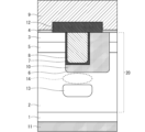
- FIG. 1 is a longitudinal cross-sectional view showing the configuration of a silicon carbide semiconductor device according to Embodiment 1.
- FIG. 1 is a longitudinal cross-sectional view showing a method for manufacturing a silicon carbide semiconductor device according to a first embodiment.
- FIG. 1 is a longitudinal cross-sectional view showing a method for manufacturing a silicon carbide semiconductor device according to a first embodiment.
- FIG. 1 is a longitudinal cross-sectional view showing a method for manufacturing a silicon carbide semiconductor device according to a first embodiment.
- FIG. 1 is a longitudinal cross-sectional view showing a method for manufacturing a silicon carbide semiconductor device according to a first embodiment.
- FIG. 1 is a longitudinal cross-sectional view showing a method for manufacturing a silicon carbide semiconductor device according to a first embodiment.
- FIG. 1 is a longitudinal cross-sectional view showing a method for manufacturing a silicon carbide semiconductor device according to a first embodiment.
- FIG. 1 is a longitudinal cross-sectional view showing a method for manufacturing a silicon carbide semiconductor device according to a first embodiment.
- FIG. 1 is a plan view showing the configuration of a silicon carbide semiconductor device according to Embodiment 1.
- FIG. 1 is a longitudinal cross-sectional view showing the configuration of a silicon carbide semiconductor device according to Embodiment 1.
- FIG. 2 is a longitudinal cross-sectional view showing the configuration of a silicon carbide semiconductor device according to a second embodiment.
- FIG. 2 is a longitudinal cross-sectional view showing the configuration of a silicon carbide semiconductor device according to a second embodiment.
- 3 is a plan view showing the configuration of a silicon carbide semiconductor device according to Embodiment 3.
- FIG. 3 is a longitudinal cross-sectional view showing the configuration of a silicon carbide semiconductor device according to a third embodiment.
- FIG. 3 is a longitudinal cross-sectional view showing the configuration of a silicon carbide semiconductor device according to a third embodiment.
- FIG. 3 is a longitudinal cross-sectional view showing the configuration of a silicon carbide semiconductor device according to a fourth embodiment.
- FIG. 7 is a block diagram showing the configuration of a power conversion system to which a power conversion device according to a fifth embodiment is applied.
- the "impurity concentration" of each region indicates the highest value (peak value) of impurities in that region.
- the first conductivity type is n type and the second conductivity type is p type
- the first conductivity type may be p type and the second conductivity type may be n type.
- FIG. 1 is a longitudinal cross-sectional view showing the configuration of a silicon carbide semiconductor device according to Embodiment 1.
- the silicon carbide semiconductor device according to the first embodiment is formed using a first conductivity type (n-type) semiconductor substrate 1 made of silicon carbide.
- the semiconductor substrate 1 is 4H-SiC, which belongs to the hexagonal crystal polymorphism of silicon carbide, and the surface of the semiconductor substrate 1 has an angle of 1 degree or more and 8 degrees or less with respect to the (11-20) plane. Assume that it is tilted at an angle. This angle of inclination is called the "off angle.”
- a semiconductor layer 20 made of silicon carbide is formed on the semiconductor substrate 1.
- This semiconductor layer 20 is formed by epitaxially growing silicon carbide of a first conductivity type whose impurity concentration is lower than that of semiconductor substrate 1 .
- a second conductivity type body region 5 is formed in the surface layer portion of the drift layer 2. Further, a first conductivity type source region 3 is formed in the surface layer portion of the body region 5 .
- the drift layer 2 is a semiconductor region of the first conductivity type that is formed on the semiconductor substrate 1 and has an impurity concentration lower than that of the semiconductor substrate 1.
- the body region 5 is a second conductivity type semiconductor region formed on the drift layer 2 .
- Source region 3 is a first conductivity type semiconductor region formed on body region 5 .
- a trench 6 is formed on the upper surface of the semiconductor layer 20, penetrating the source region 3 and the body region 5 and reaching the drift layer 2.
- the trenches 6 are formed in a stripe shape (that is, a plurality of lines arranged at equal intervals) extending in the ⁇ 11-20> direction of the semiconductor layer 20 in plan view.
- a Schottky electrode 10 is formed at the bottom of the trench 6.
- the Schottky electrode 10 is in contact with the drift layer 2 at least on the bottom surface of the trench 6, and forms a Schottky contact with the drift layer 2.
- the Schottky electrode 10 is a metal film containing Ti or Mo or metal silicide.
- the Schottky electrode 10 is connected to the source electrode 9 in a region not shown in FIG.
- a gate electrode 8 is formed on the gate insulating film 7 so as to be embedded in the trench 6 .
- Gate electrode 8 faces source region 3 , body region 5 , and drift layer 2 via gate insulating film 7 .
- Schottky electrode 10 and gate electrode 8 are insulated by gate insulating film 7 .
- An interlayer insulating film 12 is formed on the semiconductor layer 20 so as to cover the gate electrode 8 in the trench 6.
- a contact hole reaching the source region 3 is formed in the interlayer insulating film 12, and a source contact electrode 4 is formed on the source region 3 exposed at the bottom of the contact hole.
- the source contact electrode 4 is silicide formed by a reaction between a metal such as Ni or Ti and the source region 3, and forms an ohmic contact with the source region 3.
- a source electrode 9 is formed on the interlayer insulating film 12. Source electrode 9 is connected to source contact electrode 4 through a contact hole. Therefore, source electrode 9 is electrically connected to source region 3 via source contact electrode 4 .
- drain electrode 11 is formed on the back surface of the semiconductor substrate 1. Drain electrode 11 is electrically connected to semiconductor substrate 1 .
- a "well contact region" of the second conductivity type which is in contact with the source contact electrode 4 and has a higher impurity concentration than the body region 5, may be formed in a part of the surface layer of the body region 5.
- the well contact region functions to form an ohmic contact with the source contact electrode 4 and to electrically connect the source contact electrode 4 and the body region 5 with low resistance.
- the impurity concentration of the first conductivity type of the drift layer 2 is preferably 1.0 ⁇ 10 14 cm ⁇ 3 or more and 1.0 ⁇ 10 17 cm ⁇ 3 or less, and is set based on the breakdown voltage required for the silicon carbide semiconductor device. be done.
- the second conductivity type impurity concentration of body region 5 is preferably 1.0 ⁇ 10 14 cm ⁇ 3 or more and 1.0 ⁇ 10 18 cm ⁇ 3 or less.
- the impurity concentration of the first conductivity type in the source region 3 is preferably 1.0 ⁇ 10 18 cm ⁇ 3 or more and 1.0 ⁇ 10 21 cm ⁇ 3 or less.
- the second conductivity type impurity concentration in the well contact region (not shown) is preferably 1.0 ⁇ 10 18 cm ⁇ 3 or more and 1.0 ⁇ 10 21 cm ⁇ 3 or less.
- a second conductivity type protection region 13 is formed below the trench 6 in the drift layer 2 .
- the impurity concentration of the protection region 13 is preferably 0.2 times or more and twice or less the impurity concentration of the body region 5.
- the protection region 13 is spaced apart from the trench 6. Therefore, a semiconductor region of the first conductivity type, which is a part of the drift layer 2, exists between the protection region 13 and the bottom of the trench 6. Hereinafter, this area will be referred to as the "separated area 14.”
- a voltage equal to or higher than the threshold voltage is applied to gate electrode 8 , a channel with an inverted conductivity type, that is, a channel of the first conductivity type, is formed along the side surface of trench 6 in body region 5 .
- a current path of the same conductivity type is formed between the source electrode 9 and the drain electrode 11, and a current flows through the current path.
- the state in which a voltage equal to or higher than the threshold voltage is applied to gate electrode 8 in this manner is the ON state of the silicon carbide semiconductor device.
- the gate electrode 8 when a voltage lower than the threshold voltage is applied to the gate electrode 8, no channel is formed in the body region 5, and no current path is formed as in the case of the on state. Therefore, even if a voltage is applied between the drain electrode 11 and the source electrode 9, almost no current flows from the drain electrode 11 to the source electrode 9. In this way, the state in which the voltage of gate electrode 8 is equal to or lower than the threshold voltage is the off state of the silicon carbide semiconductor device. By controlling the voltage applied to gate electrode 8, the silicon carbide semiconductor device is switched between an on state and an off state.
- a unipolar current flows between Schottky electrode 10 and drain electrode 11.
- the unipolar current increases for a while, but when the potential difference between the source electrode 9 and the drain electrode 11 reaches a certain value, the voltage between the body region 5 and the drain electrode 11 and the protective region 13 increases.
- a bipolar current derived from the pn junction between body region 5 and drift layer 2 and the pn junction between protection region 13 and drift layer 2 flows between and drain electrode 11 .
- the unipolar current that can flow immediately before the bipolar current starts flowing is referred to as the "maximum unipolar current.”
- the magnitude of the maximum unipolar current is influenced by the pn junction between the body region 5 and the drift layer 2, the pn junction between the protective region 13 and the drift layer 2, and the potential difference that occurs in the drift layer 2. If a path through which the unipolar current flows can be secured and the maximum unipolar current can be maintained high, the effect of suppressing the bipolar operation of the parasitic pn diode can be sufficiently obtained.
- FIGS. 2 to 7 are longitudinal cross-sectional views showing each step of the method for manufacturing a silicon carbide semiconductor device according to the first embodiment.
- a method for manufacturing a silicon carbide semiconductor device according to the first embodiment will be described with reference to these figures.
- a semiconductor substrate 1 on which a first conductivity type drift layer 2 made of a silicon carbide semiconductor is formed is prepared. Specifically, a first conductivity type drift layer 2 is formed on a first conductivity type semiconductor substrate 1 made of silicon carbide by an epitaxial growth method. Then, as shown in FIG. 2, a source region 3 and a body region 5 are formed in the surface layer portion of the semiconductor layer 20 by ion implantation. In the semiconductor layer 20, the region of the first conductivity type that remains without the source region 3 and body region 5 formed becomes the drift layer 2.
- a well contact region having a higher impurity concentration of the second conductivity type than the body region 5 may be formed in the surface layer of the body region 5 by selective ion implantation using a mask or the like.
- ions such as N and P are implanted as donors, and when forming the second conductivity type region, ions such as Al and B are implanted as acceptors. Injected. Note that the order in which the above regions are formed does not matter. Further, all or part of those regions may be formed by epitaxial growth instead of ion implantation.
- a trench 6 is formed from the surface of the semiconductor layer 20, penetrating the source region 3 and body region 5 and reaching the drift layer 2, by reactive ion etching (RIE) or dry etching.
- RIE reactive ion etching
- a second conductivity type protection region 13 is formed below the trench 6 in the drift layer 2, as shown in FIG.
- Protective region 13 is formed apart from trench 6 .
- a region of the first conductivity type between the protection region 13 and the trench 6 becomes a separation region 14 .
- Protective region 13 and spacing region 14 may also be formed by epitaxial growth instead of ion implantation.
- heat treatment is performed to electrically activate the impurity implanted into the semiconductor layer 20.
- This heat treatment is preferably performed in an inert gas atmosphere such as argon or nitrogen, or in vacuum at a temperature of 1500° C. or more and 2200° C. or less for a time of 0.5 minutes or more and 60 minutes or less. Further, this heat treatment may be performed with the surface of the semiconductor layer 20 covered with a protective film made of carbon. In this case, it is possible to prevent the surface of the semiconductor layer 20 from becoming rough due to etching due to reaction with residual moisture or residual oxygen in the heat treatment apparatus.
- a Schottky electrode 10 in contact with the drift layer 2 is formed at the bottom of the trench 6.
- a gate insulating film 7 is formed to cover the side surfaces of the trench 6 and the top surface of the Schottky electrode 10, and the gate insulating film 7 is formed on the gate insulating film 7 so as to be buried in the trench 6. form.
- an interlayer insulating film 12 is formed on the semiconductor layer 20 so as to cover the gate electrode 8. Then, a contact hole reaching the source region 3 is formed in the interlayer insulating film 12 by selective etching using a resist mask or the like. Then, as shown in FIG. 6, a source contact electrode 4 is formed on the source region 3 exposed at the bottom of the contact hole. When the well contact region is formed in the above step, the contact hole and source contact electrode 4 are also formed on the well contact region.
- the method for forming the source contact electrode 4 is to form a metal film containing Ni as a main component over the entire surface of the interlayer insulating film 12 included in the contact hole, and then carbonize the metal film by heat treatment at 600°C or higher and 1100°C or lower.
- One method is to react with a silicon semiconductor to form a silicide film that will become the source contact electrode 4, and then remove the unreacted metal film on the interlayer insulating film 12 by wet etching. After removing the unreacted metal film on the interlayer insulating film 12, another heat treatment may be performed. By performing the second heat treatment at a higher temperature than the previous heat treatment, an ohmic contact with lower contact resistance is formed.
- a source electrode 9 is formed on the interlayer insulating film 12 to be connected to the source contact electrode 4 through a contact hole, and a drain electrode 11 is further formed on the back surface of the semiconductor substrate 1, thereby achieving the structure shown in FIG. A silicon carbide semiconductor device is obtained.
- FIG. 8 is a plan view showing the configuration of the silicon carbide semiconductor device according to the first embodiment.
- illustration of the source contact electrode 4, the source electrode 9, and the interlayer insulating film 12 is omitted, and the structure of the upper surface of the semiconductor layer 20 is shown.
- the gate electrode 8 can be formed by a chemical deposition method
- the Schottky electrode 10, the source electrode 9, and the drain electrode 11 can be formed by a physical vapor deposition method such as a sputtering method.
- FIG. 8 a longitudinal cross-sectional view taken along the line A1-A2 perpendicular to the ⁇ 11-20> direction corresponds to FIG.
- a longitudinal cross-sectional view along the line B1-B2 parallel to ⁇ 11-20> is shown in FIG.
- a portion of the Schottky electrode 10 is drawn out to the upper surface of the semiconductor layer 20 through an opening provided in the gate electrode 8.
- the gate insulating film 7 is also formed on the side surface of the Schottky electrode 10 within the opening provided in the gate electrode 8, thereby ensuring insulation between the gate electrode 8 and the Schottky electrode 10.
- the source electrode 9 is connected to a Schottky electrode 10 drawn out to the upper surface of the semiconductor layer 20 through a contact hole formed in the interlayer insulating film 12.
- the source electrode 9 and the Schottky electrode 10 may be connected.
- the Schottky electrode 10 is arranged at the bottom of the trench 6 in which the gate electrode 8 is embedded, so that the area where the Schottky electrode 10 is provided is widened in the lateral direction of FIG. There's no need to take it. Thereby, the chip area can be reduced and the chip cost can be reduced.
- the protective region 13 below the Schottky electrode 10 the electric field concentration at the bottom of the trench 6 is alleviated. Thereby, even if the Schottky electrode 10 is made thicker in order to increase the area of the Schottky barrier diode (that is, the contact area between the Schottky electrode 10 and the drift layer 2), a decrease in breakdown voltage is suppressed.
- the protection region 13 is separated from the trench 6, the area of the Schottky barrier diode is not reduced by the protection region 13. Therefore, a path for the unipolar current flowing from the Schottky electrode 10 to the drain electrode 11 is secured, and the maximum unipolar current is maintained high. Thereby, the effect of suppressing the bipolar operation of the parasitic pn diode can be sufficiently obtained.
- the area of the Schottky barrier diode can be increased while suppressing a decrease in breakdown voltage.
- the effect of suppressing the bipolar operation of the parasitic pn diode is sufficiently obtained, and the reliability of the silicon carbide semiconductor device is improved.
- the presence of the separation region 14 under the trench 6 may increase the electric field at the corner of the bottom of the trench 6 when a high voltage is applied to the drain electrode 11; Since the Schottky electrode 10 is formed, leakage current flowing from the drain electrode 11 to the gate electrode 8 via the gate insulating film 7 is suppressed.
- the width (length in the width direction) of the Schottky electrode 10 may be made larger than the thickness (length in the depth direction of the trench 6) of the Schottky electrode 10. That is, as shown in FIG. 1, when the width of the Schottky electrode 10 is w and the thickness of the Schottky electrode 10 is h, the relationship w>h may be satisfied. In this case, the rate of increase in the area of the Schottky barrier diode due to the provision of the separation region 14 becomes large, and the effect of increasing the maximum unipolar current due to the separation region 14 becomes high.
- the protection region 13 may be electrically connected to the source electrode 9 and the source region 3, or may be electrically floating. When the potential of the protection region 13 is set to floating, no bipolar current flows between the protection region 13 and the drain electrode 11, so that the maximum unipolar current can be increased.
- some of the plurality of protection regions 13 may be made electrically floating, and other parts may be electrically connected to the source electrode 9 and the source region 3.
- the protective region 13 placed in a region where bipolar current is likely to flow such as the edge of the chip, is set to a floating potential
- the protective region 13 placed in a region where leakage current is likely to occur when off such as the center of the active region, is set to a floating potential.
- bipolar current can be suppressed and breakdown voltage can be improved.
- FIG. 10 is a longitudinal cross-sectional view showing the configuration of a silicon carbide semiconductor device according to a second embodiment.
- the structure of the silicon carbide semiconductor device shown in FIG. 10 is different from the structure shown in FIG. It is something that Since the other components are the same as those in FIG. 1, their description will be omitted here.
- the resistance of the unipolar current path flowing from the Schottky electrode 10 to the drain electrode 11 is reduced, so that the maximum unipolar current is further reduced than in the first embodiment. Current can be increased.
- the low resistance region 15 may be formed so as to be in contact with the Schottky electrode 10. For example, as shown in FIG. 11, if the low resistance region 15 is brought into contact with the bottom and side surfaces of the Schottky electrode 10, the resistance of the current path of the unipolar current flowing from the bottom and side surfaces of the Schottky electrode 10 to the drain electrode 11 can be reduced. can.
- FIG. 12 is a plan view showing the configuration of a silicon carbide semiconductor device according to the third embodiment, and corresponds to FIG. 8 shown in the first embodiment.
- a longitudinal cross-sectional view taken along the line A1-A2 perpendicular to the ⁇ 11-20> direction is the same as that in FIG.
- a vertical cross-sectional view of B1-B2 parallel to ⁇ 11-20> is shown in FIG.
- FIG. 14 shows a longitudinal cross-sectional view along the C1-C2 line perpendicular to the ⁇ 11-20> direction.
- Embodiment 3 as shown in FIG. 12, a locally recessed portion is provided on the side surface of the trench 6.
- the trench 6 has locally wide portions.
- the Schottky electrode 10 is drawn out to the upper surface of the semiconductor layer 20 at a location where the side surface of the trench 6 is recessed, and is connected to the source contact electrode 4. Therefore, it is not necessary to provide the gate electrode 8 with an opening as shown in FIGS. 8 and 9 in the first embodiment. Therefore, as shown in FIGS. 12 and 13, each of the gate electrodes 8 can be formed into a continuous line.
- each of the gate electrodes 8 can be formed into a continuous line, so that the Schottky electrode 10 can be drawn out at any position.
- each of the gate electrodes 8 may be provided with a plurality of extraction points for the Schottky electrodes 10.
- FIG. 15 is a plan view showing the configuration of a silicon carbide semiconductor device according to Embodiment 4, and corresponds to the longitudinal cross-sectional view taken along line B1-B2 shown in FIG.
- the planar shape of the protection area 13 can be diversified.
- a plurality of island-shaped protection regions 13 may be arranged below the trench 6.
- the island-shaped protection regions 13 are spaced apart from each other, so the path of the unipolar current flowing from the Schottky electrode 10 to the drain electrode 11 is different from that in the case where the protection regions 13 are continuous as shown in FIG. can be expanded and the maximum unipolar current can be increased.
- the electrically floating protection regions 13 when some of the plurality of protection regions 13 are made electrically floating and the other parts are electrically connected to the source electrode 9 and the source region 3, the electrically floating protection regions 13 are , each may be formed into an island shape.
- the silicon carbide semiconductor device according to the first to fourth embodiments described above is applied to a power conversion device.
- Application of the silicon carbide semiconductor devices according to Embodiments 1 to 4 is not limited to a specific power conversion device, but hereinafter, as Embodiment 5, the silicon carbide semiconductor devices according to Embodiments 1 to 4 are applied to a three-phase inverter. A case where a silicon carbide semiconductor device is applied will be described.
- FIG. 16 is a block diagram showing the configuration of a power conversion system to which the power conversion device according to the present embodiment is applied.
- the power conversion system shown in FIG. 16 includes a power source 100, a power conversion device 200, and a load 300.
- Power supply 100 is a DC power supply and supplies DC power to power conversion device 200.
- the power source 100 can be composed of various things, for example, it can be composed of a DC system, a solar battery, a storage battery, or it can be composed of a rectifier circuit or an AC/DC converter connected to an AC system. Good too.
- the power supply 100 may be configured with a DC/DC converter that converts DC power output from a DC system into predetermined power.
- the power conversion device 200 is a three-phase inverter connected between the power source 100 and the load 300, converts the DC power supplied from the power source 100 into AC power, and supplies the AC power to the load 300.
- the power conversion device 200 includes a main conversion circuit 201 that converts DC power into AC power and outputs it, and a drive circuit 202 that outputs a drive signal that drives each switching element of the main conversion circuit 201. , and a control circuit 203 that outputs a control signal for controlling the drive circuit 202 to the drive circuit 202.
- the load 300 is a three-phase electric motor driven by AC power supplied from the power conversion device 200.
- the load 300 is not limited to a specific application, but is a motor installed in various electrical devices, and is used, for example, as a motor for a hybrid vehicle, an electric vehicle, a railway vehicle, an elevator, or an air conditioner.
- the main conversion circuit 201 includes a switching element and a freewheeling diode (not shown), and when the switching element switches, it converts DC power supplied from the power supply 100 into AC power, and supplies the alternating current power to the load 300.
- the main conversion circuit 201 is a two-level three-phase full bridge circuit, and has six switching elements and each switching element. It can be constructed from six freewheeling diodes arranged in antiparallel.
- the silicon carbide semiconductor device according to any one of the first to fourth embodiments described above is applied to each switching element and each freewheeling diode of main conversion circuit 201.
- the six switching elements are connected in series every two switching elements to constitute upper and lower arms, and each upper and lower arm constitutes each phase (U phase, V phase, W phase) of the full bridge circuit.
- the output terminals of the upper and lower arms that is, the three output terminals of the main conversion circuit 201, are connected to the load 300.
- the drive circuit 202 generates a drive signal to drive the switching element of the main conversion circuit 201 and supplies it to the control electrode of the switching element of the main conversion circuit 201. Specifically, according to a control signal from a control circuit 203, which will be described later, a drive signal that turns the switching element on and a drive signal that turns the switching element off are output to the control electrode of each switching element.
- the drive signal is a voltage signal (on signal) that is greater than or equal to the threshold voltage of the switching element, and when the switching element is kept in the off state, the drive signal is a voltage signal that is less than or equal to the threshold voltage of the switching element. signal (off signal).
- the control circuit 203 controls the switching elements of the main conversion circuit 201 so that the desired power is supplied to the load 300. Specifically, based on the power to be supplied to the load 300, the time (on time) during which each switching element of the main conversion circuit 201 should be in the on state is calculated. For example, the main conversion circuit 201 can be controlled by PWM control that modulates the on-time of the switching element according to the voltage to be output. Then, a control command (control signal) is output to the drive circuit 202 so that an on signal is output to the switching element that should be in the on state at each time, and an off signal is output to the switching element that is to be in the off state. The drive circuit 202 outputs an on signal or an off signal as a drive signal to the control electrode of each switching element in accordance with this control signal.
- the silicon carbide semiconductor device according to Embodiments 1 to 4 is applied as the switching element of main conversion circuit 201, so that reliability can be improved.
- the silicon carbide semiconductor devices according to Embodiments 1 to 4 are applied to a two-level three-phase inverter.
- the invention is not limited to this, and can be applied to various power conversion devices.
- a two-level power converter is used, but a three-level or multi-level power converter may also be used, and in the case of supplying power to a single-phase load, a single-phase inverter is used.
- the silicon carbide semiconductor devices according to 1 to 4 may be applied.
- the silicon carbide semiconductor devices according to Embodiments 1 to 4 can be applied to a DC/DC converter or an AC/DC converter.
- the power conversion device to which the silicon carbide semiconductor device according to Embodiments 1 to 4 is applied is not limited to the case where the above-mentioned load is an electric motor, but is, for example, an electrical discharge machine, a laser processing machine, or an induction heating machine. It can also be used as a power supply device for a cooker or a non-contact power supply system, and can also be used as a power conditioner for a solar power generation system, a power storage system, etc.
Landscapes
- Engineering & Computer Science (AREA)
- Microelectronics & Electronic Packaging (AREA)
- Power Engineering (AREA)
- Physics & Mathematics (AREA)
- Ceramic Engineering (AREA)
- Condensed Matter Physics & Semiconductors (AREA)
- General Physics & Mathematics (AREA)
- Computer Hardware Design (AREA)
- Electrodes Of Semiconductors (AREA)
Abstract
炭化珪素半導体装置は、半導体層(20)の上面に、ソース領域(3)およびボディ領域(5)を貫通してドリフト層(2)に達するトレンチ(6)を有する。トレンチ(6)内の底部には、ショットキー電極(10)が形成されている。トレンチ(6)の側面およびショットキー電極(10)の上面を覆うようにゲート絶縁膜(7)が形成されている。ゲート絶縁膜(7)上には、トレンチ(6)内に埋め込まれるようにゲート電極(8)が形成されている。ドリフト層(2)におけるトレンチ(6)の下方には、トレンチ(6)から離間して保護領域13が形成されている。
Description
本開示は、炭化珪素半導体装置および電力変換装置に関するものである。
MOSFET(Metal Oxide Semiconductor Field Effect Transistor)等のユニポーラ型のスイッチング素子を備える半導体装置に、ユニポーラ型の還流ダイオードとしてショットキーバリアダイオード(SBD:Schottky barrier diode)を内蔵させた電力制御用の半導体装置が知られている。当該半導体装置は、還流ダイオードを外付けする必要がないため、コストの低減に寄与できる。
炭化珪素(SiC)を母材として用いたMOSFETには、寄生pnダイオードのバイポーラ動作によるキャリアの再結合エネルギーに起因する結晶欠陥の拡張により、素子の信頼性が損なわれるという問題がある。上記の半導体装置では、MOSFETにショットキーバリアダイオードが内蔵されることで、寄生pnダイオードのバイポーラ動作を抑制できるというメリットもある。
MOSFETとしては、半導体層に形成されたトレンチ内にゲート電極が埋め込まれたトレンチゲート型のMOSFETと、半導体層の表面上にゲート電極が配置されたプレーナ型MOSFETとがある。トレンチゲート型のMOSFETは、トレンチの側壁にチャネルを形成できる分、プレーナ型MOSFETよりもチャネル幅密度を向上でき、オン抵抗を低減できる。
例えば特許文献1には、トレンチゲート型MOSFETを備える半導体装置にショットキーバリアダイオードを内蔵させる方法として、ゲート電極が埋め込まれるトレンチの底部にショットキー電極を設けることで、当該トレンチの底部にショットキーバリアダイオードを形成する技術が開示されている。この技術によれば、MOSFETセルとショットキーバリアダイオードセルとを並べて配置するよりもMOSFETセルのピッチを小さくできる。そのため、ショットキーバリアダイオードを内蔵させることによるオン抵抗の増加を抑制しつつ、MOSFETの寄生pnダイオードのバイポーラ動作を抑制することができる。
特許文献1の半導体装置のように、ゲート電極が埋め込まれるトレンチの底部にショットキーバリアダイオードを設ける場合、十分な耐圧を確保するために、ショットキー電極の厚さ(すなわち、深さ方向の長さ)は制限される。そのため、ショットキーバリアダイオードの面積を大きくできず、ショットキーバリアダイオードとMOSFETのドレイン電極との間の抵抗は高くなる。その結果、寄生pnダイオードのバイポーラ動作を抑制する効果が十分に得られないことがある。
本開示は以上のような課題を解決するためになされたものであり、ゲート電極が埋め込まれるトレンチの底部にショットキーバリアダイオードを設けた構造の炭化珪素半導体装置において、耐圧の低下を抑制しつつ、ショットキーバリアダイオードの面積を大きくすることを目的とする。
本開示に係る炭化珪素半導体装置は、炭化珪素からなる半導体層に形成された第1導電型のドリフト層と、前記半導体層の表層部に形成された第2導電型のボディ領域と、前記ボディ領域の表層部に形成された第1導電型のソース領域と、前記ソース領域および前記ボディ領域を貫通して前記ドリフト層に達するトレンチと、前記トレンチ内の底部に形成されたショットキー電極と、前記トレンチの側面および前記ショットキー電極の上面を覆うゲート絶縁膜と、前記トレンチ内に埋め込まれるように、前記ゲート絶縁膜上に形成されたゲート電極と、前記ドリフト層における前記トレンチの下方に、前記トレンチから離間して形成された第2導電型の保護領域と、を備える。
本開示に係る炭化珪素半導体装置によれば、保護領域によってトレンチ底部の電界集中が緩和されるため、ショットキー電極を厚くしても耐圧の低下は抑制される。また、保護領域はトレンチから離間しているため、保護領域によってショットキーバリアダイオードの面積が狭められることはない。よって、耐圧の低下を抑制しつつ、ショットキーバリアダイオードの面積を大きくすることができる。その結果、寄生pnダイオードのバイポーラ動作を抑制する効果が十分に得られる。
本開示の目的、特徴、態様、および利点は、以下の詳細な説明と添付図面とによって、より明白となる。
本開示に係る技術の実施の形態について説明する。以下の説明において、各領域の「不純物濃度」とは、その領域における不純物の最高値(ピーク値)を示すものとする。また、第1導電型をn型、第2導電型をp型として説明するが、それとは逆に、第1導電型をp型、第2導電型をn型としてもよい。
<実施の形態1>
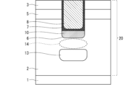
図1は、実施の形態1に係る炭化珪素半導体装置の構成を示す縦断面図である。図1に示すように、実施の形態1に係る炭化珪素半導体装置は、炭化珪素からなる第1導電型(n型)の半導体基板1を用いて形成されている。ここでは、半導体基板1は、炭化珪素の結晶多形のうち六方晶系に属する4H-SiCであり、半導体基板1の表面は、(11-20)面に対して1度以上8度以下の角度で傾いているものとする。この傾きの角度は「オフ角」と呼ばれる。
図1は、実施の形態1に係る炭化珪素半導体装置の構成を示す縦断面図である。図1に示すように、実施の形態1に係る炭化珪素半導体装置は、炭化珪素からなる第1導電型(n型)の半導体基板1を用いて形成されている。ここでは、半導体基板1は、炭化珪素の結晶多形のうち六方晶系に属する4H-SiCであり、半導体基板1の表面は、(11-20)面に対して1度以上8度以下の角度で傾いているものとする。この傾きの角度は「オフ角」と呼ばれる。
半導体基板1上には、炭化珪素からなる半導体層20が形成されている。この半導体層20は、不純物濃度が半導体基板1よりも低い第1導電型の炭化珪素をエピタキシャル成長させることによって形成される。
ドリフト層2の表層部には、第2導電型のボディ領域5が形成されている。さらに、ボディ領域5の表層部には、第1導電型のソース領域3が形成されている。半導体層20おいて、ソース領域3およびボディ領域5が形成されずに残った第1導電型の領域は、ドリフト層2となる。つまり、ドリフト層2は、半導体基板1上に形成され、不純物濃度が半導体基板1よりも低い第1導電型の半導体領域である。また、ボディ領域5は、ドリフト層2上に形成された第2導電型の半導体領域である。ソース領域3は、ボディ領域5上に形成された第1導電型の半導体領域である。
半導体層20の上面には、ソース領域3およびボディ領域5を貫通してドリフト層2に達するトレンチ6が形成されている。トレンチ6は、平面視で、半導体層20の〈11-20〉方向に伸びるストライプ状(すなわち等間隔に並ぶ複数のライン状)に形成されている。
トレンチ6の底部には、ショットキー電極10が形成されている。ショットキー電極10は、トレンチ6の少なくとも底面でドリフト層2に接しており、ドリフト層2との間でショットキーコンタクトを形成する。ここでは、ショットキー電極10は、TiあるいはMoを含む金属膜または金属シリサイドとした。ショットキー電極10は、図1では不図示の領域で、ソース電極9と接続されている。
トレンチ6の側面およびショットキー電極10の上面は、ゲート絶縁膜7で覆われている。ゲート絶縁膜7の上には、ゲート電極8が、トレンチ6に埋め込まれるように形成されている。ゲート電極8は、ゲート絶縁膜7を介して、ソース領域3、ボディ領域5およびドリフト層2に面している。ショットキー電極10とゲート電極8との間は、ゲート絶縁膜7によって絶縁されている。
半導体層20上には、トレンチ6内のゲート電極8を覆うように層間絶縁膜12が形成されている。層間絶縁膜12には、ソース領域3に達するコンタクトホールが形成されており、コンタクトホールの底に露出したソース領域3上にソースコンタクト電極4が形成されている。ソースコンタクト電極4は、NiやTi等の金属とソース領域3とが反応して形成されたシリサイドであり、ソース領域3との間でオーミックコンタクトを形成する。
層間絶縁膜12の上には、ソース電極9が形成されている。ソース電極9は、コンタクトホールを通してソースコンタクト電極4に接続している。よって、ソース電極9は、ソースコンタクト電極4を介してソース領域3と電気的に接続される。
また、半導体基板1の裏面にはドレイン電極11が形成されている。ドレイン電極11は、半導体基板1と電気的に接続されている。
図示は省略するが、ボディ領域5の表層部の一部に、ソースコンタクト電極4に接し、ボディ領域5よりも不純物濃度が高い第2導電型の「ウェルコンタクト領域」が形成されてもよい。ウェルコンタクト領域は、ソースコンタクト電極4との間でオーミックコンタクトを形成し、ソースコンタクト電極4とボディ領域5との間を低抵抗で電気的に接続するように機能する。
ドリフト層2の第1導電型の不純物濃度は、1.0×1014cm-3以上、1.0×1017cm-3以下が好ましく、炭化珪素半導体装置に求められる耐圧等に基づいて設定される。ボディ領域5の第2導電型の不純物濃度は、1.0×1014cm-3以上、1.0×1018cm-3以下が好ましい。ソース領域3の第1導電型の不純物濃度は、1.0×1018cm-3以上、1.0×1021cm-3以下が好ましい。また、ウェルコンタクト領域(不図示)の第2導電型の不純物濃度は、1.0×1018cm-3以上、1.0×1021cm-3以下が好ましい。
実施の形態1に係る炭化珪素半導体装置では、ドリフト層2におけるトレンチ6の下方に第2導電型の保護領域13が形成されている。保護領域13の不純物濃度は、ボディ領域5の不純物濃度の0.2倍以上、2倍以下であることが好ましい。
保護領域13は、トレンチ6から離間している。よって、保護領域13とトレンチ6の底部との間には、ドリフト層2の一部である第1導電型の半導体領域が存在する。以下、この領域を「離間領域14」と称す。
図1に示す炭化珪素半導体装置の動作について簡単に説明する。ゲート電極8に閾値電圧以上の電圧が印加されると、ボディ領域5において、導電型が反転したチャネル、すなわち第1導電型のチャネルがトレンチ6の側面に沿って形成される。それにより、ソース電極9からドレイン電極11までの間に同一導電型の電流経路が形成され、その電流経路に電流が流れる。このようにゲート電極8に閾値電圧以上の電圧が印加された状態が、炭化珪素半導体装置のオン状態となる。また、ゲート電極8に閾値電圧未満の電圧が印加されると、ボディ領域5にはチャネルが形成されず、オン状態の場合のような電流経路は形成されない。そのため、ドレイン電極11とソース電極9との間に電圧が印加されても、ドレイン電極11からソース電極9へは電流がほとんど流れない。このようにゲート電極8の電圧が閾値電圧以下の状態が、炭化珪素半導体装置のオフ状態となる。ゲート電極8に印加する電圧を制御することによって、炭化珪素半導体装置のオン状態とオフ状態とが切り換わる。
炭化珪素半導体装置のオフ状態において、ショットキー電極10が構成するショットキーバリアダイオードに順方向電圧が印加されると、ショットキー電極10とドレイン電極11との間にユニポーラ電流が流れる。この順方向電圧を上げていくと、しばらくはユニポーラ電流が増加するが、ソース電極9とドレイン電極11との電位差がある値に達すると、ボディ領域5とドレイン電極11との間および保護領域13とドレイン電極11との間に、ボディ領域5とドリフト層2との間のpn接合および保護領域13とドリフト層2との間のpn接合に由来したバイポーラ電流が流れる。バイポーラ電流が流れ始める直前に流すことができるユニポーラ電流を「最大ユニポーラ電流」と称す。
最大ユニポーラ電流の大きさは、ボディ領域5とドリフト層2との間のpn接合や、保護領域13とドリフト層2との間のpn接合、ドリフト層2に生じる電位差によって影響される。ユニポーラ電流の流れる経路を確保して、最大ユニポーラ電流を高く維持することできれば、寄生pnダイオードのバイポーラ動作を抑制する効果を十分に得ることができる。
図2から図7は、実施の形態1に係る炭化珪素半導体装置の製造方法の各工程を示す縦断面図である。以下、これらの図を参照しつつ、実施の形態1に係る炭化珪素半導体装置の製造方法を説明する。
まず、炭化珪素半導体からなる第1導電型のドリフト層2が形成された半導体基板1を用意する。具体的には、炭化珪素からなる第1導電型の半導体基板1上に、第1導電型のドリフト層2をエピタキシャル成長法によって形成する。そして、図2のように、半導体層20の表層部にソース領域3およびボディ領域5を、それぞれイオン注入によって形成する。半導体層20おいて、ソース領域3およびボディ領域5が形成されずに残った第1導電型の領域が、ドリフト層2となる。図示は省略するが、マスクを用いた選択的なイオン注入などにより、ボディ領域5の表層部に、ボディ領域5よりも第2導電型の不純物濃度が高いウェルコンタクト領域を形成してもよい。
上記の工程で、第1導電型領域を形成するときは、ドナーとして例えばNやP等のイオンが注入され、第2導電型領域を形成するときは、アクセプタとして例えばAlやB等のイオンが注入される。なお、上記の各領域を形成する順序は問わない。また、それらの領域の全部または一部は、イオン注入ではなくエピタキシャル成長によって形成されてもよい。
次に、反応性イオンエッチング(RIE)またはドライエッチングによって、図3のように、半導体層20の表面からソース領域3およびボディ領域5を貫通してドリフト層2に達するトレンチ6を形成する。
続いて、トレンチ6の底面へのイオン注入によって、図4のように、ドリフト層2におけるトレンチ6の下方に、第2導電型の保護領域13を形成する。保護領域13は、トレンチ6から離間して形成される。保護領域13とトレンチ6との間に第1導電型の領域が、離間領域14となる。保護領域13および離間領域14も、イオン注入ではなくエピタキシャル成長によって形成してもよい。
その後、半導体層20に注入した不純物を電気的に活性化させるための熱処理を行う。この熱処理は、アルゴンまたは窒素等の不活性ガス雰囲気、若しくは、真空中で、1500℃以上、2200℃以下の温度、0.5分以上、60分以下の時間で行うとよい。また、この熱処理は、半導体層20の表面を炭素からなる保護膜で覆った状態で行ってもよい。その場合、熱処理装置内の残留水分や残留酸素との反応によるエッチングで半導体層20の表面が荒れることを抑止できる。
その後、図5のように、トレンチ6内の底部に、ドリフト層2と接するショットキー電極10を形成する。そして、図6のように、トレンチ6の側面およびショットキー電極10の上面を覆うようにゲート絶縁膜7を形成し、ゲート絶縁膜7の上に、トレンチ6に埋め込まれるようにゲート絶縁膜7を形成する。
その後、半導体層20上に、ゲート電極8を覆うように層間絶縁膜12を形成する。そして、レジストマスク等を用いた選択的なエッチング等により、層間絶縁膜12にソース領域3に達するコンタクトホールを形成する。そして、図6のように、当該コンタクトホールの底に露出したソース領域3上にソースコンタクト電極4を形成する。上の工程でウェルコンタクト領域を形成した場合、コンタクトホールおよびソースコンタクト電極4は、ウェルコンタクト領域上にも形成される。
ソースコンタクト電極4の形成方法としては、コンタクトホール内の含む層間絶縁膜12上の全面にNiを主成分とする金属膜を成膜し、600℃以上、1100℃以下の熱処理により金属膜を炭化珪素半導体と反応させて、ソースコンタクト電極4となるシリサイド膜を形成し、その後、層間絶縁膜12上の未反応の金属膜をウェットエッチングにより除去する、という方法が挙げられる。層間絶縁膜12上の未反応の金属膜を除去した後に、再度の熱処理を行ってもよい。再度の熱処理を先の熱処理よりも高温で行うことで、コンタクト抵抗のより低いオーミックコンタクトが形成される。
その後、層間絶縁膜12上に、コンタクトホールを通してソースコンタクト電極4に接続するソース電極9を形成し、さらに、半導体基板1の裏面にドレイン電極11を形成することで、図1に示した構造の炭化珪素半導体装置が得られる。
図8は、実施の形態1に係る炭化珪素半導体装置の構成を示す平面図である。図8においては、ソースコンタクト電極4、ソース電極9および層間絶縁膜12の図示が省略されており、半導体層20の上面の構成が示されている。なお、ゲート電極8は、化学堆積法で形成することができ、ショットキー電極10、ソース電極9およびドレイン電極11は、スパッタ法などの物理蒸着法で形成することができる。
図8において〈11-20〉方向に垂直なA1-A2線に沿った縦断面図は、図1に対応する。〈11-20〉と平行なB1-B2線に沿った縦断面図を、図9に示す。図9のように、ショットキー電極10の一部は、ゲート電極8に設けられた開口を通して半導体層20の上面に引き出されている。なお、ゲート絶縁膜7は、ゲート電極8に設けられた開口内のショットキー電極10の側面にも形成されており、それにより、ゲート電極8とショットキー電極10との絶縁は確保されている。また、ソース電極9は、層間絶縁膜12に形成されたコンタクトホールを通して、半導体層20の上面に引き出されたショットキー電極10に接続されている。
あるいは、ショットキー電極10をトレンチ6の底部のみに形成し、ゲート電極8に設けられた開口内に、絶縁膜を介してソース電極9の一部を埋め込むことで、ソース電極9とショットキー電極10とを接続させてもよい。
実施の形態1に係る炭化珪素半導体装置では、ショットキー電極10が、ゲート電極8が埋め込まれるトレンチ6の底部に配置されるため、図1の横方向において、ショットキー電極10を設ける領域を広くとる必要がない。それにより、チップ面積を小さくして、チップコストを安くすることができる。
また、ショットキー電極10の下方に保護領域13が設けられることで、トレンチ6の底部の電界集中が緩和される。それにより、ショットキーバリアダイオードの面積(つまり、ショットキー電極10とドリフト層2との接触面積)を大きくするためにショットキー電極10を厚くしても耐圧の低下は抑制される。
さらに、保護領域13が、トレンチ6から離間しているため、保護領域13によってショットキーバリアダイオードの面積が狭められることはない。よって、ショットキー電極10からドレイン電極11へ流れるユニポーラ電流の経路が確保され、最大ユニポーラ電流が高く維持される。それにより、寄生pnダイオードのバイポーラ動作を抑制する効果が十分に得られる。
以上より、実施の形態1に係る炭化珪素半導体装置によれば、耐圧の低下を抑制しつつ、ショットキーバリアダイオードの面積を大きくすることができる。その結果、寄生pnダイオードのバイポーラ動作を抑制する効果が十分に得られ、炭化珪素半導体装置の信頼性が向上する。
なお、トレンチ6の下に離間領域14が存在することで、ドレイン電極11に高電圧が印加されたときにトレンチ6の底の角部の電界が高くなるおそれがあるが、トレンチ6の底部にショットキー電極10が形成されているため、ドレイン電極11からゲート絶縁膜7を介してゲート電極8へ流れるリーク電流は抑制される。
また、ショットキー電極10の幅(短手方向の長さ)を、ショットキー電極10の厚さ(トレンチ6の深さ方向の長さ)よりも大きくしてもよい。すなわち、図1のように、ショットキー電極10の幅をw、ショットキー電極10の厚さをhとすると、w>hの関係となるようにしてもよい。その場合、離間領域14を設けたことによるショットキーバリアダイオードの面積の増加率が大きくなり、離間領域14による最大ユニポーラ電流の増加効果が高くなる。
保護領域13は、ソース電極9およびソース領域3と電気的に接続させてもよいし、電気的にフローティングでもよい。保護領域13の電位をフローティングにした場合、保護領域13とドレイン電極11との間にバイポーラ電流が流れなくなるため、最大ユニポーラ電流を増加させることができる。
また、複数の保護領域13のうちの一部を電気的にフローティングとし、他の一部をソース電極9およびソース領域3と電気的に接続させてもよい。この場合、チップの端部などバイポーラ電流が流れやすい領域に配置される保護領域13をフローティング電位にし、活性領域の中央部などオフ時のリーク電流が発生しやすい領域に配置される保護領域13をソース電位にすると、バイポーラ電流を抑制しつつ耐圧を向上させることができる。
<実施の形態2>
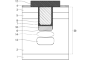
図10は、実施の形態2に係る炭化珪素半導体装置の構成を示す縦断面図である。図10に示す炭化珪素半導体装置の構成は、図1の構成に対し、トレンチ6と保護領域13との間に、ドリフト層2よりも不純物濃度が高い第1導電型の低抵抗領域15を設けたものである。その他の構成要素は図1と同様であるため、ここではそれらの説明は省略する。
図10は、実施の形態2に係る炭化珪素半導体装置の構成を示す縦断面図である。図10に示す炭化珪素半導体装置の構成は、図1の構成に対し、トレンチ6と保護領域13との間に、ドリフト層2よりも不純物濃度が高い第1導電型の低抵抗領域15を設けたものである。その他の構成要素は図1と同様であるため、ここではそれらの説明は省略する。
トレンチ6と保護領域13との間に低抵抗領域15が設けられることで、ショットキー電極10からドレイン電極11へ流れるユニポーラ電流の経路の抵抗が小さくなるため、実施の形態1よりもさらに最大ユニポーラ電流を増加させることができる。
低抵抗領域15は、ショットキー電極10と接するように形成されてもよい。例えば図11のように、低抵抗領域15がショットキー電極10の底面および側面に接するようにすれば、ショットキー電極10の底および側面からドレイン電極11へ流れるユニポーラ電流の電流経路の抵抗を小さくできる。
<実施の形態3>
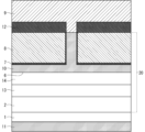
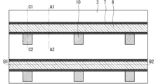
図12は、実施の形態3に係る炭化珪素半導体装置の構成を示す平面図であり、実施の形態1で示した図8に対応している。図12において、〈11-20〉方向に垂直なA1-A2線に沿った縦断面図は、図1と同様である。〈11-20〉と平行なB1-B2の縦断面図を、図13に示す。また、〈11-20〉方向と垂直なC1-C2線に沿った縦断面図を、図14に示す。
図12は、実施の形態3に係る炭化珪素半導体装置の構成を示す平面図であり、実施の形態1で示した図8に対応している。図12において、〈11-20〉方向に垂直なA1-A2線に沿った縦断面図は、図1と同様である。〈11-20〉と平行なB1-B2の縦断面図を、図13に示す。また、〈11-20〉方向と垂直なC1-C2線に沿った縦断面図を、図14に示す。
実施の形態3では、図12のように、トレンチ6の側面には、局所的に凹んだ箇所が設けられている。つまり、トレンチ6は、局所的に幅の広い箇所を有している。ショットキー電極10は、図14のように、トレンチ6の側面が凹んだ箇所で半導体層20の上面に引き出され、ソースコンタクト電極4に接続している。そのため、ゲート電極8には、実施の形態1で図8および図9に示したような開口を設ける必要がない。よって、図12および図13のように、ゲート電極8のそれぞれを連続的なライン状にすることができる。
図8および図9に示したゲート電極8は、ショットキー電極10を引き出すための開口によって断線するため、ショットキー電極10の引き出し箇所を設ける位置や数に制約がある。それに対し、実施の形態3では、ゲート電極8のそれぞれを連続的なライン状にできるため、ショットキー電極10の引き出し箇所を任意の位置に配置できる。例えば、ゲート電極8のそれぞれにショットキー電極10の引き出し箇所を複数設けることもできる。
<実施の形態4>
図15は、実施の形態4に係る炭化珪素半導体装置の構成を示す平面図であり、図8に示したB1-B2の縦断面図に対応する。
図15は、実施の形態4に係る炭化珪素半導体装置の構成を示す平面図であり、図8に示したB1-B2の縦断面図に対応する。
保護領域13を電気的にフローティングとした場合、保護領域13の平面形状の多様化が可能になる。例えば図15に示すように、トレンチ6の下方に島状の保護領域13を複数個並べて配置してもよい。図15の構成では、島状の保護領域13は互いに離間しているため、図8のように保護領域13が連続的な場合に比べ、ショットキー電極10からドレイン電極11へ流れるユニポーラ電流の経路が広がり、最大ユニポーラ電流を増加させることができる。
また、複数の保護領域13のうちの一部を電気的にフローティングとし、他の一部をソース電極9およびソース領域3と電気的に接続させる場合には、電気的にフローティングな保護領域13を、それぞれ島状に形成してもよい。
<実施の形態5>
本実施の形態は、上述した実施の形態1から4に係る炭化珪素半導体装置を電力変換装置に適用したものである。実施の形態1から4に係る炭化珪素半導体装置の適用は特定の電力変換装置に限定されるものではないが、以下、実施の形態5として、三相のインバータに実施の形態1から4に係る炭化珪素半導体装置を適用した場合について説明する。
本実施の形態は、上述した実施の形態1から4に係る炭化珪素半導体装置を電力変換装置に適用したものである。実施の形態1から4に係る炭化珪素半導体装置の適用は特定の電力変換装置に限定されるものではないが、以下、実施の形態5として、三相のインバータに実施の形態1から4に係る炭化珪素半導体装置を適用した場合について説明する。
図16は、本実施の形態に係る電力変換装置を適用した電力変換システムの構成を示すブロック図である。
図16に示す電力変換システムは、電源100、電力変換装置200、負荷300から構成される。電源100は、直流電源であり、電力変換装置200に直流電力を供給する。電源100は種々のもので構成することが可能であり、例えば、直流系統、太陽電池、蓄電池で構成することができるし、交流系統に接続された整流回路やAC/DCコンバータで構成することとしてもよい。また、電源100を、直流系統から出力される直流電力を所定の電力に変換するDC/DCコンバータによって構成することとしてもよい。
電力変換装置200は、電源100と負荷300の間に接続された三相のインバータであり、電源100から供給された直流電力を交流電力に変換し、負荷300に交流電力を供給する。電力変換装置200は、図16に示すように、直流電力を交流電力に変換して出力する主変換回路201と、主変換回路201の各スイッチング素子を駆動する駆動信号を出力する駆動回路202と、駆動回路202を制御する制御信号を駆動回路202に出力する制御回路203とを備えている。
負荷300は、電力変換装置200から供給された交流電力によって駆動される三相の電動機である。なお、負荷300は特定の用途に限られるものではなく、各種電気機器に搭載された電動機であり、例えば、ハイブリッド自動車や電気自動車、鉄道車両、エレベーター、もしくは、空調機器向けの電動機として用いられる。
以下、電力変換装置200の詳細を説明する。主変換回路201は、スイッチング素子と還流ダイオードを備えており(図示せず)、スイッチング素子がスイッチングすることによって、電源100から供給される直流電力を交流電力に変換し、負荷300に供給する。主変換回路201の具体的な回路構成は種々のものがあるが、本実施の形態に係る主変換回路201は2レベルの三相フルブリッジ回路であり、6つのスイッチング素子とそれぞれのスイッチング素子に逆並列された6つの還流ダイオードから構成することができる。主変換回路201の各スイッチング素子および各還流ダイオードには、上述した実施の形態1から4のいずれかに係る炭化珪素半導体装置を適用する。6つのスイッチング素子は2つのスイッチング素子ごとに直列接続され上下アームを構成し、各上下アームはフルブリッジ回路の各相(U相、V相、W相)を構成する。そして、各上下アームの出力端子、すなわち主変換回路201の3つの出力端子は、負荷300に接続される。
駆動回路202は、主変換回路201のスイッチング素子を駆動する駆動信号を生成し、主変換回路201のスイッチング素子の制御電極に供給する。具体的には、後述する制御回路203からの制御信号に従い、スイッチング素子をオン状態にする駆動信号とスイッチング素子をオフ状態にする駆動信号とを各スイッチング素子の制御電極に出力する。スイッチング素子をオン状態に維持する場合、駆動信号はスイッチング素子の閾値電圧以上の電圧信号(オン信号)であり、スイッチング素子をオフ状態に維持する場合、駆動信号はスイッチング素子の閾値電圧以下の電圧信号(オフ信号)となる。
制御回路203は、負荷300に所望の電力が供給されるよう主変換回路201のスイッチング素子を制御する。具体的には、負荷300に供給すべき電力に基づいて主変換回路201の各スイッチング素子がオン状態となるべき時間(オン時間)を算出する。例えば、出力すべき電圧に応じてスイッチング素子のオン時間を変調するPWM制御によって主変換回路201を制御することができる。そして、各時点においてオン状態となるべきスイッチング素子にはオン信号を、オフ状態となるべきスイッチング素子にはオフ信号が出力されるよう、駆動回路202に制御指令(制御信号)を出力する。駆動回路202は、この制御信号に従い、各スイッチング素子の制御電極にオン信号またはオフ信号を駆動信号として出力する。
本実施の形態に係る電力変換装置では、主変換回路201のスイッチング素子として実施の形態1から4に係る炭化珪素半導体装置を適用するため、信頼性向上を実現することができる。
本実施の形態では、2レベルの三相インバータに実施の形態1から4に係る炭化珪素半導体装置を適用する例を説明したが、実施の形態1から4に係る炭化珪素半導体装置の適用は、これに限られるものではなく、種々の電力変換装置に適用することができる。本実施の形態では、2レベルの電力変換装置としたが3レベルやマルチレベルの電力変換装置であっても構わないし、単相負荷に電力を供給する場合には単相のインバータに実施の形態1から4に係る炭化珪素半導体装置を適用しても構わない。また、直流負荷等に電力を供給する場合にはDC/DCコンバータやAC/DCコンバータに実施の形態1から4に係る炭化珪素半導体装置を適用することも可能である。
また、実施の形態1から4に係る炭化珪素半導体装置を適用した電力変換装置は、上述した負荷が電動機の場合に限定されるものではなく、例えば、放電加工機やレーザー加工機、または誘導加熱調理器や非接触給電システムの電源装置として用いることもでき、さらには太陽光発電システムや蓄電システム等のパワーコンディショナーとして用いることも可能である。
なお、各実施の形態を自由に組み合わせたり、各実施の形態を適宜、変形、省略したりすることが可能である。
上記した説明は、すべての態様において、例示であって、例示されていない無数の変形例が想定され得るものと解される。
1 半導体基板、2 ドリフト層、3 ソース領域、4 ソースコンタクト電極、5 ボディ領域、6 トレンチ、7 ゲート絶縁膜、8 ゲート電極、9 ソース電極、10 ショットキー電極、11 ドレイン電極、12 層間絶縁膜、13 保護領域、14 離間領域、15 低抵抗領域、20 半導体層、100 電源、200 電力変換装置、201 主変換回路、202 駆動回路、203 制御回路、300 負荷。
Claims (12)
- 炭化珪素からなる半導体層に形成された第1導電型のドリフト層と、
前記半導体層の表層部に形成された第2導電型のボディ領域と、
前記ボディ領域の表層部に形成された第1導電型のソース領域と、
前記ソース領域および前記ボディ領域を貫通して前記ドリフト層に達するトレンチと、
前記トレンチ内の底部に形成されたショットキー電極と、
前記トレンチの側面および前記ショットキー電極の上面を覆うゲート絶縁膜と、
前記トレンチ内に埋め込まれるように、前記ゲート絶縁膜上に形成されたゲート電極と、
前記ドリフト層における前記トレンチの下方に、前記トレンチから離間して形成された第2導電型の保護領域と、
を備える炭化珪素半導体装置。 - 前記ショットキー電極の幅は、前記ショットキー電極の厚さよりも大きい、
請求項1に記載の炭化珪素半導体装置。 - 前記保護領域の不純物濃度は、前記ボディ領域の不純物濃度の0.2倍以上、2倍以下である、
請求項1または請求項2に記載の炭化珪素半導体装置。 - 前記保護領域は、電気的にフローティングである、
請求項1から請求項3のいずれか一項に記載の炭化珪素半導体装置。 - 前記トレンチの下方に、島状の前記保護領域が複数並べて形成されている、
請求項4に記載の炭化珪素半導体装置。 - 前記トレンチおよび前記保護領域を複数備え、
複数の前記保護領域のうちの一部は電気的にフローティングであり、他の一部は前記ソース領域と電気的に接続している、
請求項1から請求項3のいずれか一項に記載の炭化珪素半導体装置。 - 複数の前記保護領域のうち電気的にフローティングな前記保護領域は、それぞれ島状に形成されている、
請求項6に記載の炭化珪素半導体装置。 - 前記トレンチと前記保護領域との間に、前記ドリフト層よりも不純物濃度が高い第1導電型の低抵抗領域が形成されている、
請求項1から請求項7のいずれか一項に記載の炭化珪素半導体装置。 - 前記低抵抗領域は、前記ショットキー電極に接している、
請求項8に記載の炭化珪素半導体装置。 - 請求項1から請求項9のいずれか一項に記載の炭化珪素半導体装置を有し、入力される電力を変換して出力する主変換回路と、
前記炭化珪素半導体装置を駆動する駆動信号を前記炭化珪素半導体装置に出力する駆動回路と、
前記駆動回路を制御する制御信号を前記駆動回路に出力する制御回路と、
を備えた電力変換装置。 - 炭化珪素からなる半導体層に第1導電型のドリフト層を形成する工程と、
前記半導体層の表層部に第2導電型のボディ領域を形成する工程と、
前記ボディ領域の表層部に第1導電型のソース領域を形成する工程と、
前記ソース領域および前記ボディ領域を貫通して前記ドリフト層に達するトレンチを形成する工程と、
前記ドリフト層における前記トレンチの下方に、前記トレンチから離間して第2導電型の保護領域を形成する工程と、
前記トレンチ内の底部にショットキー電極を形成する工程と、
前記トレンチの側面および前記ショットキー電極の上面を覆うゲート絶縁膜を形成する工程と、
前記トレンチに埋め込まれるように、前記ゲート絶縁膜上にゲート電極を形成する工程と、
を備える炭化珪素半導体装置の製造方法。 - 前記ショットキー電極を形成する工程は、物理蒸着法で行われ、
前記ゲート電極を形成する工程は、化学堆積法で行われる、
請求項11に記載の炭化珪素半導体装置の製造方法。
Priority Applications (1)
| Application Number | Priority Date | Filing Date | Title |
|---|---|---|---|
| PCT/JP2022/030967 WO2024038504A1 (ja) | 2022-08-16 | 2022-08-16 | 炭化珪素半導体装置、電力変換装置および炭化珪素半導体装置の製造方法 |
Applications Claiming Priority (1)
| Application Number | Priority Date | Filing Date | Title |
|---|---|---|---|
| PCT/JP2022/030967 WO2024038504A1 (ja) | 2022-08-16 | 2022-08-16 | 炭化珪素半導体装置、電力変換装置および炭化珪素半導体装置の製造方法 |
Publications (1)
| Publication Number | Publication Date |
|---|---|
| WO2024038504A1 true WO2024038504A1 (ja) | 2024-02-22 |
Family
ID=89941535
Family Applications (1)
| Application Number | Title | Priority Date | Filing Date |
|---|---|---|---|
| PCT/JP2022/030967 WO2024038504A1 (ja) | 2022-08-16 | 2022-08-16 | 炭化珪素半導体装置、電力変換装置および炭化珪素半導体装置の製造方法 |
Country Status (1)
| Country | Link |
|---|---|
| WO (1) | WO2024038504A1 (ja) |
Citations (7)
| Publication number | Priority date | Publication date | Assignee | Title |
|---|---|---|---|---|
| JP2010109221A (ja) * | 2008-10-31 | 2010-05-13 | Rohm Co Ltd | 半導体装置 |
| JP2013089778A (ja) * | 2011-10-18 | 2013-05-13 | Toyota Motor Corp | 半導体装置及びその製造方法 |
| JP2016009712A (ja) * | 2014-06-23 | 2016-01-18 | 住友電気工業株式会社 | 炭化珪素半導体装置 |
| CN206657811U (zh) * | 2017-04-06 | 2017-11-21 | 淄博汉林半导体有限公司 | 一种内建肖特基界面的垂直场效应二极管 |
| CN109192779A (zh) * | 2018-08-28 | 2019-01-11 | 电子科技大学 | 一种碳化硅mosfet器件及其制造方法 |
| JP2020087958A (ja) * | 2018-11-15 | 2020-06-04 | ルネサスエレクトロニクス株式会社 | 半導体装置 |
| CN212542447U (zh) * | 2020-07-24 | 2021-02-12 | 淄博汉林半导体有限公司 | 一种新型立体导电的肖特基二极管 |
-
2022
- 2022-08-16 WO PCT/JP2022/030967 patent/WO2024038504A1/ja unknown
Patent Citations (7)
| Publication number | Priority date | Publication date | Assignee | Title |
|---|---|---|---|---|
| JP2010109221A (ja) * | 2008-10-31 | 2010-05-13 | Rohm Co Ltd | 半導体装置 |
| JP2013089778A (ja) * | 2011-10-18 | 2013-05-13 | Toyota Motor Corp | 半導体装置及びその製造方法 |
| JP2016009712A (ja) * | 2014-06-23 | 2016-01-18 | 住友電気工業株式会社 | 炭化珪素半導体装置 |
| CN206657811U (zh) * | 2017-04-06 | 2017-11-21 | 淄博汉林半导体有限公司 | 一种内建肖特基界面的垂直场效应二极管 |
| CN109192779A (zh) * | 2018-08-28 | 2019-01-11 | 电子科技大学 | 一种碳化硅mosfet器件及其制造方法 |
| JP2020087958A (ja) * | 2018-11-15 | 2020-06-04 | ルネサスエレクトロニクス株式会社 | 半導体装置 |
| CN212542447U (zh) * | 2020-07-24 | 2021-02-12 | 淄博汉林半导体有限公司 | 一种新型立体导电的肖特基二极管 |
Similar Documents
| Publication | Publication Date | Title |
|---|---|---|
| US11158704B2 (en) | Semiconductor device and power conversion device | |
| JP6929404B2 (ja) | 炭化珪素半導体装置および電力変換装置 | |
| US11637184B2 (en) | Silicon carbide semiconductor device, power converter, method of manufacturing silicon carbide semiconductor device, and method of manufacturing power converter | |
| US11984492B2 (en) | Silicon carbide semiconductor device, power converter, and method of manufacturing silicon carbide semiconductor device | |
| CN110709997A (zh) | 半导体装置以及电力变换装置 | |
| JP6735950B1 (ja) | 炭化珪素半導体装置、電力変換装置および炭化珪素半導体装置の製造方法 | |
| US11063122B2 (en) | Silicon carbide semiconductor device and power conversion device | |
| CN115101596A (zh) | 碳化硅半导体装置以及电力变换装置 | |
| JP6874158B2 (ja) | 炭化珪素半導体装置および電力変換装置 | |
| JP6641523B2 (ja) | 半導体装置および電力変換装置 | |
| JP6991370B2 (ja) | 半導体装置及び電力変換装置 | |
| JP7275407B1 (ja) | 炭化珪素半導体装置、電力変換装置および炭化珪素半導体装置の製造方法 | |
| JP6873273B2 (ja) | 炭化珪素半導体装置および電力変換装置 | |
| JP7047981B1 (ja) | 炭化珪素半導体装置および電力変換装置 | |
| JP7370476B2 (ja) | 炭化珪素半導体装置の製造方法、炭化珪素半導体装置および電力変換装置 | |
| WO2024038504A1 (ja) | 炭化珪素半導体装置、電力変換装置および炭化珪素半導体装置の製造方法 | |
| US11894428B2 (en) | Silicon carbide semiconductor device and power converter | |
| CN116325176A (zh) | 碳化硅半导体装置以及电力变换装置 | |
| JP7332812B2 (ja) | 炭化珪素半導体装置および電力変換装置 | |
| WO2022190269A1 (ja) | 炭化珪素半導体装置とその製造方法、および、電力変換装置 | |
| WO2024024073A1 (ja) | 半導体装置、電力変換装置および半導体装置の製造方法 | |
| WO2022249397A1 (ja) | 半導体装置及び電力変換装置 | |
| CN117642873A (zh) | 碳化硅半导体装置以及使用碳化硅半导体装置的电力变换装置 |
Legal Events
| Date | Code | Title | Description |
|---|---|---|---|
| 121 | Ep: the epo has been informed by wipo that ep was designated in this application |
Ref document number: 22955678 Country of ref document: EP Kind code of ref document: A1 |