WO2024034482A1 - 半導体装置、及び半導体装置の製造方法 - Google Patents
半導体装置、及び半導体装置の製造方法 Download PDFInfo
- Publication number
- WO2024034482A1 WO2024034482A1 PCT/JP2023/028203 JP2023028203W WO2024034482A1 WO 2024034482 A1 WO2024034482 A1 WO 2024034482A1 JP 2023028203 W JP2023028203 W JP 2023028203W WO 2024034482 A1 WO2024034482 A1 WO 2024034482A1
- Authority
- WO
- WIPO (PCT)
- Prior art keywords
- bonding
- semiconductor device
- semiconductor element
- electrode pad
- manufacturing
- Prior art date
- Legal status (The legal status is an assumption and is not a legal conclusion. Google has not performed a legal analysis and makes no representation as to the accuracy of the status listed.)
- Ceased
Links
Images




Classifications
-
- H—ELECTRICITY
- H10—SEMICONDUCTOR DEVICES; ELECTRIC SOLID-STATE DEVICES NOT OTHERWISE PROVIDED FOR
- H10W—GENERIC PACKAGES, INTERCONNECTIONS, CONNECTORS OR OTHER CONSTRUCTIONAL DETAILS OF DEVICES COVERED BY CLASS H10
- H10W70/00—Package substrates; Interposers; Redistribution layers [RDL]
- H10W70/60—Insulating or insulated package substrates; Interposers; Redistribution layers
-
- H—ELECTRICITY
- H10—SEMICONDUCTOR DEVICES; ELECTRIC SOLID-STATE DEVICES NOT OTHERWISE PROVIDED FOR
- H10W—GENERIC PACKAGES, INTERCONNECTIONS, CONNECTORS OR OTHER CONSTRUCTIONAL DETAILS OF DEVICES COVERED BY CLASS H10
- H10W72/00—Interconnections or connectors in packages
- H10W72/071—Connecting or disconnecting
Definitions
- the present disclosure relates to a semiconductor device and a method for manufacturing a semiconductor device.
- semiconductor devices that include a semiconductor element such as a semiconductor laser chip and a submount for mounting the semiconductor element (for example, Patent Document 1, Patent Document 2, etc.).
- a semiconductor element such as a semiconductor laser chip
- a submount for mounting the semiconductor element for example, Patent Document 1, Patent Document 2, etc.
- the bonding surface of the semiconductor element is bonded to the bonding surface of the submount using a bonding member such as solder.
- a transfer device such as a collet is generally used to press the semiconductor device against the bonding member at a predetermined position on the submount. After melting by heating, the joining member is cooled. Thereby, the bonding member solidifies while in contact with the semiconductor element and the submount, so that the semiconductor element can be bonded to the submount via the bonding member.
- the bonding member may protrude outward from between the bonding surface of the semiconductor element and the bonding surface of the submount.
- the amount of bonding material between the bonding surface of the semiconductor element and the bonding surface of the submount decreases, which may make it impossible to ensure sufficient bonding strength.
- the bonding member protrudes the semiconductor element may move from a predetermined position together with the bonding member.
- the present disclosure has been made to solve such problems, and aims to provide a semiconductor device and the like that can suppress protrusion of a bonding member from between a bonding surface of a semiconductor element and a bonding surface of a submount. purpose.
- a semiconductor device includes a semiconductor element, a submount, and a bonded body, wherein the semiconductor element is arranged in an element body and in the element body.
- a first base electrode having a first bonding surface that is bonded to the bonded body
- the submount includes a base and a second bond that is disposed on the base and bonded to the bonded body.
- the bonded body is an alloy containing a plurality of metal elements, and is bonded to the semiconductor element in a first bonding region of the first bonding surface;
- the semiconductor element is a non-bonded part disposed outside the first bonding area on the first bonding surface, and has a composition different from that of the bonded body. , and further includes a non-bonded portion made of at least one metal element among the plurality of metal elements, and the area of the first bonding region is smaller than the area of the second bonding region.
- a method for manufacturing a semiconductor device is a method for manufacturing a semiconductor device including a semiconductor element and a submount, the semiconductor element comprising an element body and a submount. a first base electrode disposed and having a first bonding surface; and a first electrode pad disposed on the first bonding surface; the submount includes a base; and the submount is disposed on the base; The method for manufacturing a semiconductor device includes a second base electrode having a second bonding surface and a second electrode pad disposed on the second bonding surface, and the method includes bonding the semiconductor element to the second electrode pad.
- the first electrode pad and the first electrode pad are prepared by preparing the submount on which the member is placed, and by starting to place the semiconductor element on the bonding member using a transfer machine that moves the semiconductor element.
- the transfer machine includes a placing step of bringing the semiconductor element into contact with the joining member, a melting step of melting the joining member, and a solidifying step of solidifying the joining member, and in the melting step, the transfer machine places the semiconductor element on the joining member.
- the pressing force is calculated as follows: WG ( ⁇ s - ⁇ c )/ ⁇ is less than 10 times c .
- FIG. 1 is a top view showing the overall configuration of a semiconductor device according to an embodiment.
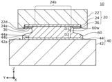
- 1 is a cross-sectional view showing the overall configuration of a semiconductor device according to an embodiment.
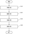
- 1 is a flowchart showing the flow of a method for manufacturing a semiconductor device according to an embodiment.
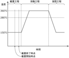
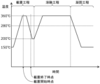
- 7 is a schematic graph showing an example of a control mode of heater temperature in a mounting step, a melting step, and a solidifying step of the method for manufacturing a semiconductor device according to an embodiment.
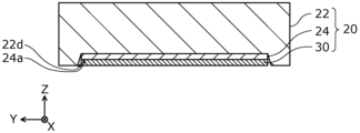
- FIG. 2 is a schematic cross-sectional view showing a semiconductor element prepared in a preparation step of a method for manufacturing a semiconductor device according to an embodiment.
- FIG. 3 is a schematic cross-sectional view showing a submount prepared in a preparation step of a method for manufacturing a semiconductor device according to an embodiment.
- FIG. 2 is a schematic top view showing the configuration of a submount according to an embodiment.
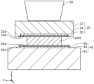
- FIG. 3 is a schematic cross-sectional view showing a mounting step of a method for manufacturing a semiconductor device according to an embodiment.
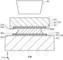
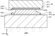
- FIG. 2 is a first schematic cross-sectional view showing a melting step of a method for manufacturing a semiconductor device according to an embodiment.
- FIG. 7 is a second schematic cross-sectional view showing a melting step of the method for manufacturing a semiconductor device according to the embodiment.
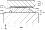
- FIG. 7 is a third schematic cross-sectional view showing the melting step of the method for manufacturing a semiconductor device according to the embodiment.
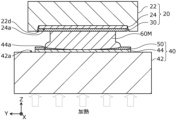
- FIG. 7 is a fourth schematic cross-sectional view showing the melting step of the method for manufacturing a semiconductor device according to the embodiment.
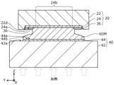
- FIG. 7 is a fifth schematic cross-sectional view showing a melting step of the method for manufacturing a semiconductor device according to the embodiment.
- FIG. 2 is a schematic cross-sectional view showing a solidification step of a method for manufacturing a semiconductor device according to an embodiment.
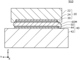
- FIG. 3 is a schematic cross-sectional view showing the configuration of a semiconductor device manufactured using a melting process of a comparative example.
- 7 is a schematic graph showing an example of a control mode of heater temperature in a mounting step, a melting step, and a solidifying step of the method for manufacturing a semiconductor device according to Modification Example 1.
- FIG. 12 is a schematic graph showing an example of a control mode of heater temperature in a mounting step, a melting step, and a solidification step of a method for manufacturing a semiconductor device according to Modification Example 2.
- FIG. 12 is a schematic graph showing an example of
- each figure is a schematic diagram and is not necessarily strictly illustrated. Therefore, the scale etc. in each figure are not necessarily the same.
- symbol is attached to the substantially the same structure, and the overlapping description is omitted or simplified.
- the terms “upper” and “lower” do not refer to vertically above and vertically downward in absolute spatial recognition, but are defined by relative positional relationships based on the order of stacking in a stacked structure. This term is used as a term that refers to Additionally, the terms “above” and “below” are used not only when two components are spaced apart and there is another component between them; This also applies when they are placed in contact with each other.
- FIGS. 1 and 2 are a top view and a cross-sectional view, respectively, showing the overall configuration of a semiconductor device 10 according to this embodiment.
- FIG. 2 shows a cross section of the semiconductor device 10 taken along line II-II in FIG. Note that each figure shows an X-axis, a Y-axis, and a Z-axis that are orthogonal to each other.
- the X, Y, and Z axes are a right-handed Cartesian coordinate system.
- the semiconductor device 10 includes a semiconductor element 20, a submount 40, and a bonded body 60.
- the semiconductor element 20 is an element that includes a semiconductor layer and has an electrode connected to the semiconductor layer.
- the semiconductor element 20 is not particularly limited, in this embodiment, it is a semiconductor light emitting element that emits light. More specifically, the semiconductor element 20 is a semiconductor laser element that emits laser light. As shown in FIG. 2, the semiconductor element 20 is arranged in the Z-axis direction with respect to the submount 40.
- the semiconductor element 20 has an element main body 22, a first base electrode 24, and a non-bonded part 36.
- the element body 22 is the main body portion of the semiconductor element 20 and includes a semiconductor layer.
- the element body 22 includes, for example, a substrate made of GaAs, an n-type semiconductor layer, an active layer, and a p-type semiconductor layer.
- a recess 22d is formed in the surface of the element body 22 that faces the submount 40.
- the recess 22d has a flat bottom surface. Note that flat here is not limited to a completely flat state, but also includes a substantially flat state. For example, a state in which the error in depth at each position of the recess 22d with respect to the average value of the depth of the recess 22d is within about 10% is also called flat.
- the dimension of the element body 22 in the X-axis direction is, for example, 120 ⁇ m or more and 150 ⁇ m or less, and the dimension in the Y-axis direction (that is, the longitudinal direction of the semiconductor element 20) is, for example, 260 ⁇ m or more and 280 ⁇ m or less.
- the first base electrode 24 is an electrode that is disposed on the element body 22 and has a first bonding surface 24a that is bonded to the bonded body 60.
- the first base electrode 24 is a metal film placed in a recess 22d formed in the element body 22.
- the first base electrode 24 is formed of a metal material that easily comes into close contact with the element body 22.
- the first base electrode 24 may be, for example, a single layer film or a multilayer film formed of at least one of Ti, Cr, Ni, Pd, and Pt.
- the first base electrode 24 includes a 100 nm thick Ti film in contact with the element body 22 and a 150 nm thick Pt film in contact with the Ti film.
- the surface of the Pt film corresponds to the first bonding surface 24a.
- the first base electrode 24 may be placed on the substrate side of the element body 22, or may be placed on the back side (semiconductor layer side) of the element body 22 with respect to the substrate.
- the non-bonding portion 36 is a metal portion located outside the first bonding area 24b on the first bonding surface 24a of the first base electrode 24.
- the first bonding area 24b is an area where the bonded body 60 is bonded on the first bonding surface 24a.
- the non-bonded portion 36 has a different composition from the bonded body 60 and is made of at least one metal element among the plurality of metal elements included in the bonded body 60.
- the non-bonded portion 36 surrounds the first bonded region 24b.
- the non-bonded portion 36 is an Au film with a thickness of 200 nm.
- the submount 40 is a member on which the semiconductor element 20 is mounted, and includes a base 42 and a second base electrode 44.
- submount 40 further includes external electrode pads 48, as shown in FIG.
- the base 42 is a member having a main surface 42a on which the second base electrode 44 is arranged.
- the base 42 has, for example, a rectangular parallelepiped shape.
- the base 42 is a Si substrate with each side of the main surface 42a having a length of 300 ⁇ m.
- the material of the base 42 is not limited to Si.
- a ceramic substrate, a polycrystalline substrate, a single crystalline substrate, or the like made of a material such as alumina, AlN, SiC, or diamond can be used.
- the second base electrode 44 is an electrode that is placed on the base 42 and has a second bonding surface 44a that is bonded to the bonded body 60.
- the second base electrode 44 is arranged on the main surface 42a of the base 42.
- the second base electrode 44 is formed of a metal material that easily comes into close contact with the base 42.
- the second base electrode 44 may be, for example, a single layer film or a multilayer film formed of at least one of Ti, Cr, Ni, Pd, and Pt.
- the second base electrode 44 includes a 100 nm thick Ti film in contact with the base 42 and a 150 nm thick Pt film in contact with the Ti film.
- the surface of the Pt film corresponds to the second bonding surface 44a.
- the external electrode pad 48 shown in FIG. 1 is an electrode pad for connecting external wiring.
- the external electrode pad 48 is arranged in a region of the second bonding surface 44a located outside the semiconductor element 20 when the second bonding surface 44a of the second base electrode 44 is viewed from above. That is, the external electrode pad 48 is arranged in a region of the second bonding surface 44a that is not covered by the semiconductor element 20.
- the external electrode pad 48 is electrically connected to the first base electrode 24 via the second base electrode 44 and the bonded body 60.
- the external electrode pad 48 is an Au film with a thickness of 200 nm.
- the joined body 60 is an alloy containing a plurality of metal elements, and joins the semiconductor element 20 and the submount 40.
- the bonded body 60 is bonded to the semiconductor element 20 at the first bonding area 24b of the first bonding surface 24a, and to the submount 40 at the second bonding area 44b of the second bonding surface 44a.
- the bonded body 60 is, for example, AuSn solder.
- the area of the first bonding region 24b is smaller than the area of the second bonding region 44b. Further, the dimension of the first bonding region 24b in the X-axis direction parallel to the first bonding surface 24a is smaller than the dimension of the second bonding region 44b in the X-axis direction, and is parallel to the first bonding surface 24a of the first bonding region 24b. The dimension in the Y-axis direction perpendicular to the X-axis direction is smaller than the dimension in the Y-axis direction of the second bonding region 44b.
- the area of the first bonding surface 24a is smaller than the area of the second bonding region 44b.
- the dimension of the first bonding surface 24a in the X-axis direction is smaller than the dimension of the second bonding region 44b in the X-axis direction, and the dimension of the first bonding surface 24a in the Y-axis direction is smaller than the dimension of the second bonding region 44b in the Y-axis direction. smaller than the dimensions.
- the area of the second bonding region 44b is smaller than the area of the semiconductor element 20 in a top view of the second bonding surface 44a.
- the dimension in the X-axis direction of the second bonding region 44b is smaller than the dimension in the X-axis direction of the semiconductor element 20 in a top view of the second bonding surface 44a
- the dimension in the Y-axis direction of the second bonding region 44b is smaller than the dimension in the Y-axis direction of the second bonding surface 44a. It is smaller than the dimension of the surface 44a in the Y-axis direction of the semiconductor element 20 when viewed from above.
- the distance D1 from the narrowest part 60w of the joined body 60 having the smallest cross-sectional area parallel to the second joint surface 44a to the first joint surface 24a is It is smaller than the distance D2 from the portion 60w to the second joint surface 44a.
- the narrowest part 60w is located closer to the second joint surface 44a than the surface of the non-joint part 36 (lower surface in FIG. 2); The location is not limited to this.
- the distance from the narrowest portion 60w to the second bonding surface 44a may be equal to the distance from the surface of the non-bonding portion 36 to the second bonding surface 44a, for example. That is, the narrowest portion 60w may be on the same plane as the surface of the non-joining portion 36.
- FIG. 3 is a flowchart showing the flow of the method for manufacturing the semiconductor device 10 according to this embodiment.
- FIG. 4 is a schematic graph showing an example of a control mode of the heater temperature in the mounting step, melting step, and solidification step of the method for manufacturing the semiconductor device 10 according to the present embodiment.
- 5A and 5B are schematic cross-sectional views showing the semiconductor element 20 and the submount 40, respectively, which are prepared in the preparation step of the method for manufacturing the semiconductor device 10 according to the present embodiment.
- 7 to 13 are schematic cross-sectional views showing each step of the method for manufacturing the semiconductor device 10 according to the present embodiment.
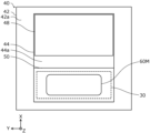
- FIG. 6 is a schematic top view showing the configuration of the submount 40 according to this embodiment.
- FIG. 6 shows the submount 40 before the semiconductor element 20 is bonded to it.
- the outline of the first electrode pad 30 of the semiconductor element 20 to be bonded to the submount 40 is shown by a broken line.
- the semiconductor element 20 shown in FIG. 5A and the submount 40 shown in FIG. 5B in which the bonding member 60M is arranged on the second electrode pad 50 are prepared (preparation step S10).
- the semiconductor element 20 includes an element body 22, a first base electrode 24, and a first electrode pad 30.
- the first electrode pad 30 is a metal film placed on the first bonding surface 24a of the first base electrode 24.
- the center portion of the first electrode pad 30 is alloyed with the bonding member 60M disposed on the submount 40 and becomes a part of the bonded body 60.
- the peripheral edge of the first electrode pad 30 is not alloyed.
- This peripheral portion of the first electrode pad 30 that is not alloyed is referred to as a non-bonded portion 36.
- the first electrode pad 30 is arranged within a recess 22d formed in the element body 22.
- the first electrode pad 30 has a different composition from the bonded body 60 and is composed of at least one metal element among the plurality of metal elements included in the bonded body 60.
- the first electrode pad 30 is an Au film with a thickness of 500 nm.
- the submount 40 includes a base 42, a second base electrode 44, and a second electrode pad 50.
- submount 40 further includes external electrode pads 48, as shown in FIG.
- the second electrode pad 50 is a metal film disposed on the second bonding surface 44a of the second base electrode 44, as shown in FIG. 5B.
- the second electrode pad 50 is alloyed with the joining member 60M and becomes a part of the joined body 60.
- the second electrode pad 50 has a different composition from the bonded body 60, and is composed of at least one metal element among the plurality of metal elements contained in the bonded body 60.
- the second electrode pad 50 is an Au film with a thickness of 200 nm.
- the joining member 60M is a member for joining the semiconductor element 20 and the submount 40, and is arranged on the second electrode pad 50. As shown in FIG. 6, in a top view of the second bonding surface 44a of the second base electrode 44, the area of the bonding member 60M is smaller than the area of the second electrode pad 50.
- the dimension of the bonding member 60M in the X-axis direction is smaller than the dimension of the second electrode pad 50 in the X-axis direction
- the dimension of the bonding member 60M in the Y-axis direction is smaller than the dimension of the second electrode pad 50 in the Y-axis direction.
- the area of the first electrode pad 30 is larger than the area of the bonding member 60M and smaller than the area of the second electrode pad 50.
- the dimension of the first electrode pad 30 in the X-axis direction is larger than the dimension of the joining member 60M in the X-axis direction, and smaller than the dimension of the second electrode pad 50 in the X-axis direction.
- the dimension of the first electrode pad 30 in the Y-axis direction is larger than the dimension of the joining member 60M in the Y-axis direction, and smaller than the dimension of the second electrode pad 50 in the Y-axis direction.
- the area of the second electrode pad 50 is smaller than the area of the semiconductor element 20.
- the dimension of the second electrode pad 50 in the X-axis direction is smaller than the dimension of the semiconductor element 20 in the X-axis direction, and the dimension of the second electrode pad 50 in the Y-axis direction is smaller than the dimension of the semiconductor element 20 in the Y-axis direction.
- the bonding member 60M has a width in the X-axis direction of 97 ⁇ m, a width in the Y-axis direction of 236 ⁇ m, and a thickness of 3.0 ⁇ m
- the first electrode pad 30 has a width in the X-axis direction of 110 ⁇ m and a width in the Y-axis direction
- the second electrode pad 50 has a width in the X-axis direction of 114 ⁇ m and a width in the Y-axis direction of 250 ⁇ m
- the semiconductor element 20 has a width in the X-axis direction of 130 ⁇ m and a width in the Y-axis direction of 260 ⁇ m.
- the shape of the bonding member 60M is a rectangular shape with the four corners removed. If the distance between the four corner parts of the joining member 60M and the end of the second electrode pad 50 is small, the four corner parts of the joining member 60M may protrude from the end of the second electrode pad 50 when the joining member 60M is melted in a later process. Although it is easy to do so, by removing the four corner portions of the joining member 60M, it is possible to prevent the joining member 60M from protruding from the second electrode pad 50. Specifically, the distance between the bonding member 60M and the end of the second electrode pad 50 may be 30 ⁇ m or more. Thereby, it is possible to suppress the melted joining member 60M from protruding from the second electrode pad 50.
- the bonding member 60M is placed on the second electrode pad 50 using, for example, a method such as vapor deposition.
- a method such as vapor deposition.
- AuSn solder can be used as the bonding member 60M.
- the mounting step S20 includes a step in which the semiconductor element 20 is moved to the vicinity of the first electrode pad 30 by the transfer machine 90, and a process in which the semiconductor element 20 is mounted on the bonding member 60M by the transfer machine 90.
- the transfer machine 90 is a device that moves the semiconductor element 20, and for example, a collet or the like can be used.
- the time when the semiconductor element 20 contacts the bonding member 60M is defined as the start of mounting, and the time when the transfer machine 90 leaves the semiconductor element 20 is defined as the end of the mounting.
- the positioning of the semiconductor element 20 with respect to the submount 40 may be performed, for example, by capturing images of the semiconductor element 20 and the submount 40 and using an image recognition technique, or may be performed by a mechanical method.
- the joining member 60M is heated at a temperature lower than the melting point of the joining member 60M. More specifically, in the mounting step S20, the heater temperature is maintained at the same temperature as the preheating temperature in the preparation step S10, thereby continuing to heat the joining member 60M at a temperature lower than the melting point of the joining member 60M. Thereby, the temperature of the joining member 60M is maintained below the melting point of the joining member 60M.
- the lower surface of the base 42 of the submount 40 may be placed on a heater.
- the heater temperature in the mounting step S20 is maintained at 150° C., which is lower than the melting point of the joining member 60M (melting point of AuSn solder, 280° C.).
- the time required for heating can be reduced by 1.25 seconds by setting the preheating temperature to 150°C, which is 125°C higher than room temperature (25°C). can.
- the joining member 60M is melted (melting step S30).
- the temperature of the bonding member 60M is heated to be higher than the melting point of the bonding member 60M.
- the joining member 60M is melted by increasing the temperature of the heater to 360°C.
- the force with which the transfer machine 90 presses the semiconductor element 20 against the joining member 60M is controlled so that the semiconductor element 20 is not buried in the melted joining member 60M.
- the semiconductor element 20 is a semiconductor laser element whose main component is GaAs
- the average specific gravity ⁇ c of the semiconductor element 20 is smaller than the specific gravity ⁇ s of the bonding member 60M, so the semiconductor element 20 is pressed against the bonding member 60M. If not, the semiconductor element 20 floats on the melted bonding member 60M.
- the semiconductor element 20 when the area of the bonding member 60M is smaller than the area of the semiconductor element 20 in the top view of the second bonding surface 44a, the semiconductor element 20 is placed on the melted bonding member 60M. Even if the semiconductor element 20 is not pressed against the joining member 60M, the joining member 60M will not protrude outside the semiconductor element 20.
- the force pressing the semiconductor element 20 against the bonding member 60M is less than the force corresponding to the difference in specific gravity between the semiconductor element 20 and the bonding member 60M, the semiconductor element 20 will not be buried in the melted bonding member 60M.
- the mass W [kg] of the semiconductor element 20 and the gravitational acceleration G [m/s 2 ] the force corresponding to the difference in specific gravity between the semiconductor element 20 and the joining member 60M is expressed as WG ( ⁇ s - ⁇ c )/ It is expressed as ⁇ c .
- the surface tension of the melted joining member 60M suppresses the spreading of the joining member 60M in the lateral direction (X-axis direction and Y-axis direction in each figure).
- the spreading suppressing force caused by this surface tension depends on the wettability of the surface on which the joining member 60M is arranged, and the higher the wettability of the surface, the smaller the spreading suppressing force.
- the force pressing the semiconductor element 20 against the bonding member 60M is 3.1 ⁇ 10 ⁇ 6 [N] or less, the bonding member 60M hardly protrudes outside the semiconductor device 20. .
- the force for pressing the semiconductor element 20 against the bonding member 60M was 1.5 ⁇ 10 ⁇ 6 [N] or less, the bonding member 60M did not protrude outside the semiconductor device 20 at all. Therefore, the force for pressing the semiconductor element 20 against the bonding member 60M may be 10 times or less of WG( ⁇ s ⁇ c )/ ⁇ c . Thereby, protrusion of the joining member 60M can be suppressed. Further, the force for pressing the semiconductor element 20 against the bonding member 60M may be 5 times or less of WG( ⁇ s ⁇ c )/ ⁇ c . Thereby, protrusion of the joining member 60M can be more reliably suppressed.
- the force with which the transfer machine 90 presses the semiconductor element 20 against the bonding member 60M is zero. As shown in FIG. 8, the transfer machine 90 may be separated from the semiconductor element 20. Thereby, protrusion of the joining member 60M can be suppressed even more reliably.
- FIG. 14 is a schematic cross-sectional view showing the configuration of a semiconductor device 910 manufactured using the melting process of the comparative example.
- the semiconductor element 20 is pressed against the bonding member 60M with a force exceeding 10 times WG( ⁇ s ⁇ c )/ ⁇ c .
- the bonding member 60M is connected between the first electrode pad 30 (or the first base electrode 24) and the second electrode pad 50 (or the second base electrode 44) (that is, the first electrode pad 30 (a region in which a line segment connecting an arbitrary point on the second electrode pad 50 and an arbitrary point on the second electrode pad 50 may exist).
- the side surface of the joining member 60M protrudes convexly from between the first electrode pad 30 and the second electrode pad 50.
- the bonding member 60M largely protrudes to the outside of the first electrode pad 30.
- the thickness of the bonding member 60M becomes thinner than a critical value, and the bonding by the bonding member 60M is reduced. Strength may be insufficient.
- the bonding member 60M protrudes in one direction, there is a possibility that the semiconductor element 20 moves from a predetermined position in that direction together with the bonding member 60M.
- the force for pressing the semiconductor element 20 against the bonding member 60M is 10 times or less of WG( ⁇ s - ⁇ c )/ ⁇ c .
- the force for pressing the semiconductor element 20 against the bonding member 60M is 10 times or less of WG( ⁇ s - ⁇ c )/ ⁇ c .
- WG( ⁇ s - ⁇ c )/ ⁇ c can be prevented from protruding. Therefore, a sufficient amount of the bonding member 60M between the first electrode pad 30 and the bonding surface of the second electrode pad 50 can be ensured (for example, the thickness of the bonding member 60M can be ensured at 2 ⁇ m or more). Accordingly, sufficient bonding strength can be obtained, and movement of the semiconductor element 20 can be suppressed.
- the joining member 60M that has been turned into a liquid phase and the portion of the second electrode pad 50 that is in contact with the joining member 60M begin to be alloyed.
- the Sn element of the bonding member 60M is diffused into the second electrode pad 50, and the region where the composition is AuSn, that is, the region of the bonding member 60M is expanded.
- the liquid-phase bonding member 60M spreads over the entire upper surface of the second electrode pad 50, as shown in FIG. In other words, the area of the lower surface of the bonding member 60M is equal to the area of the upper surface of the second electrode pad 50. Furthermore, the area of the bonding member 60M expands toward the lower surface of the second electrode pad 50.
- a part of the upper part (the part far from the submount 40) of the joining member 60M is also turned into a liquid phase.
- the joining member 60M that has been turned into a liquid phase spreads laterally. Furthermore, the bonding member 60M and the portion of the first electrode pad 30 that is in contact with the bonding member 60M begin to be alloyed. This completes the electrical connection between the semiconductor element 20 and the submount 40.
- the entire joint member 60M including the upper part is turned into a liquid phase, as shown in FIG.
- the upper part of the joining member 60M also spreads in the lateral direction, but since the lower part of the joining member 60M has a higher temperature and higher fluidity, the lower part of the joining member 60M spreads more in the lateral direction than the upper part.
- the surface tension of the joining member 60M that has been turned into a liquid phase suppresses the spread in the lateral direction.
- the entire second electrode pad 50 is alloyed with the bonding member 60M. Thereby, the submount 40 and the joining member 60M can be firmly joined. Note that the area outside the second electrode pad 50 is not alloyed with the bonding member 60M and has low wettability to the bonding member 60M, so that the bonding member 60M is difficult to spread.
- the center portion of the first electrode pad 30 is alloyed with the joining member 60M. Thereby, the semiconductor element 20 and the bonding member 60M can be firmly bonded. Further, a region corresponding to the central portion of the alloyed first electrode pad 30 is a first bonding region 24b where the bonding member 60M and the first bonding surface 24a of the first base electrode 24 are bonded. The non-bonding portion 36 located outside the center of the first electrode pad 30 is not alloyed with the bonding member 60M. When the bonding member 60M is AuSn, the non-bonding portion 36 does not contain the Sn element, and the alloy portion between the first electrode pad 30 and the bonding member 60M contains the Sn element.
- the bonding member 60M since the contact angle between the non-bonded portion 36 of the semiconductor element 20 and the melted bonding member 60M is maintained at a predetermined angle, the bonding member 60M has a constriction while the bonding member 60M is being melted. It becomes a shape with .
- the joining member 60M is solidified (solidifying step S40).
- the temperature of the joining member 60M is cooled to below the melting point of the joining member 60M.
- the temperature of the heater is cooled to 150°C.
- the joining member 60M is solidified.
- a bonded body 60 is formed as shown in FIG. 13.
- the semiconductor device 10 according to this embodiment can be manufactured.
- a method for manufacturing the semiconductor device 10 according to Modification 1 and Modification 2 of the present embodiment will be described.
- the method for manufacturing the semiconductor device 10 according to Modifications 1 and 2 differs from the method for manufacturing the semiconductor device according to the present embodiment described above in the aspect of preheating in the mounting step S20.
- the methods for manufacturing the semiconductor device 10 according to Modifications 1 and 2 will be explained with reference to FIGS. 15 and 16, respectively, focusing on the differences from the method for manufacturing the semiconductor device 10 according to the present embodiment. do.
- FIG. 15 is a schematic graph showing an example of a control mode of the heater temperature in the mounting step S20, the melting step S30, and the solidifying step S40 of the semiconductor device manufacturing method according to the first modification.
- the preheating temperature was 150°C
- the mounting step S20 according to modification example 1 as shown in FIG. 15, the preheating temperature was 150°C.
- the temperature of the submount 40 on which the joining member 60M is mounted is raised to 360° C., which is higher than the melting point (280° C.) of the joining member 60M, to melt the joining member 60M.
- the mounting is started and ended in this state, and then the temperature is lowered to 200°C.
- the mounting step S20 mounting is started with the bonding member 60M in a molten state.
- the surface shape of the bonding member 60M can be deformed when the semiconductor element 20 is placed, the posture of the semiconductor element 20 after being placed is not affected by variations in the surface shape of the bonding member 60M before being placed.
- the bonding member 60M is in a molten state at the end of the placement, the contact area between the first electrode pad 30 and the bonding member 60M during placement increases, and the transfer device 90 is separated from the semiconductor element 20. The risk that the semiconductor element 20 will sometimes remain held on the transfer machine 90 side is reduced due to the influence of surface tension and the like.
- FIG. 16 is a schematic graph showing an example of a control mode of the heater temperature in the mounting step S20, the melting step S30, and the solidifying step S40 of the semiconductor device manufacturing method according to the second modification.
- the time during which the transfer machine 90 presses the bonding member 60M via the semiconductor element 20 is longer than in the first modification.
- the placement ends in a state where the temperature of the bonding member 60M has decreased and it has solidified. That is, in the mounting step S20, the mounting is completed with the bonding member 60M solidified.
- the semiconductor element 20 and the solidified joining member 60M are joined, when the transfer machine 90 is separated from the semiconductor element 20, the semiconductor element 20 remains held on the transfer machine 90 side. Risk is further reduced.
- the semiconductor device 10 includes the semiconductor element 20, the submount 40, and the assembly 60.
- the semiconductor element 20 includes an element body 22 and a first base electrode 24 that is disposed on the element body 22 and has a first bonding surface 24a that is bonded to the bonded body 60.
- the submount 40 includes a base 42 and a second base electrode 44 that is disposed on the base 42 and has a second bonding surface 44a that is bonded to the bonded body 60.
- the bonded body 60 is an alloy containing a plurality of metal elements, and is bonded to the semiconductor element 20 in the first bonding region 24b of the first bonding surface 24a, and is bonded to the submount 40 in the second bonding region 44b of the second bonding surface 44a. It is joined with.
- the semiconductor element 20 is a non-bonded portion 36 disposed outside the first bonding region 24b on the first bonding surface 24a, and has a composition different from that of the bonded body 60 and a plurality of metal elements contained in the bonded body 60. It further includes a non-bonded portion 36 made of at least one metal element.
- the area of the first bonding region 24b is smaller than the area of the second bonding region 44b.
- the area of the first bonding surface 24a is smaller than the area of the second bonding region 44b, and the area of the second bonding region 44b is smaller than the area of the semiconductor element 20 in the top view of the second bonding surface 44a. It can be small.
- the bonded body 60 protrudes outside the semiconductor element 20. can be suppressed.
- the distance D1 from the narrowest part 60w to the first bonding surface 24a which has the smallest cross-sectional area parallel to the second bonding surface 44a of the bonded body 60, is the distance D1 from the narrowest part 60w to the second bonding surface 24a. It may be smaller than the distance D2 to 44a.
- the cross section of the bonded body 60 has a shape close to a trapezoid, with the second bonding surface side being wider.
- this shape of the joined body 60 leads to high heat dissipation characteristics.
- the entire bonded body 60 may be disposed inside the periphery of the semiconductor element 20 when viewed from above of the second bonding surface 44a.
- the bonded body 60 can be prevented from protruding outside the semiconductor element 20.
- the semiconductor element 20 may be a semiconductor light emitting element.
- the positional shift of the semiconductor element 20 can be suppressed, the shift of the optical axis of the semiconductor element 20, which is a semiconductor light emitting element, can be suppressed.
- the semiconductor element 20 is a semiconductor laser element and is used as a point light source, the required specifications for optical axis position accuracy are often strict, and the effect of suppressing positional deviation is useful.
- the semiconductor laser element emits in the lateral direction and is mounted junction-down, the bonded body 60 does not protrude outside the semiconductor laser element, so the light emitted from the semiconductor laser element is blocked by the bonded body 60. I can't get caught.
- the method for manufacturing the semiconductor device 10 includes a preparation step S10 of preparing the semiconductor element 20 and the submount 40 in which the bonding member 60M is arranged on the second electrode pad 50, and moving the semiconductor element 20.
- a mounting step S20 in which the semiconductor element 20 is placed on the bonding member 60M by the transfer machine 90 to bring the first electrode pad 30 and the bonding member 60M into contact; a melting step S30 in which the bonding member 60M is melted;
- a solidification step S40 is included in which the joining member 60M is solidified.
- the force with which the transfer machine 90 presses the semiconductor element 20 against the joining member 60M is determined by the mass W [kg] of the semiconductor element 20, the average specific gravity ⁇ c, the gravitational acceleration G [m/s2], and the joining member 60M.
- the specific gravity ⁇ s it is less than 10 times WG( ⁇ s ⁇ c)/ ⁇ c.
- the semiconductor element 20 is not pressed against the bonding member 60M with excessive force, so that the semiconductor element 20 floats on the melted bonding member 60M. Therefore, since the semiconductor element 20 can be prevented from being buried in the bonding member 60M, it is possible to suppress the bonding member 60M from protruding outside the semiconductor element 20.
- the force with which the transfer machine 90 presses the semiconductor element 20 against the bonding member 60M may be zero.
- the area of the bonding member 60M may be smaller than the area of the second electrode pad 50 in a top view of the second bonding surface 44a.
- the area of the first electrode pad 30 is larger than the area of the bonding member 60M and smaller than the area of the second electrode pad 50;
- the area of the two-electrode pad 50 may be smaller than the area of the semiconductor element 20.
- the area of the second electrode pad 50 on which the bonding member 60M is arranged is smaller than the area of the semiconductor element 20, it is possible to suppress the bonding member 60M from protruding outside the semiconductor element 20.
- the shape of the bonding member 60M may be a rectangular shape with four corners removed when viewed from above of the second bonding surface 44a.
- the bonding member 60M When the bonding member 60M is rectangular, the four corner portions of the bonding member 60M tend to protrude from the second electrode pad 50, but since the bonding member 60M does not have four corner portions, the bonding member 60M protrudes from the second electrode pad 50. can be suppressed.
- the center portion of the first electrode pad 30 may be alloyed with the bonding member 60M.
- the semiconductor element 20 and the joining member 60M can be firmly joined.
- the non-bonded portion 36 located outside the center of the first electrode pad 30 does not need to be alloyed with the bonding member 60M.
- the entire second electrode pad 50 may be alloyed with the bonding member 60M.
- the submount 40 and the joining member 60M can be firmly joined.
- the bonding member 60M may be heated at a temperature lower than the melting point of the bonding member 60M.
- the time required for further heating in the melting step S30 following the mounting step S20 can be shortened. Therefore, the time required to manufacture the semiconductor device 10 can be reduced.
- mounting may be started with the bonding member 60M in a molten state.
- the surface shape of the bonding member 60M can be deformed when the semiconductor element 20 is placed, the posture of the semiconductor element 20 after being placed is not affected by variations in the surface shape of the bonding member 60M before being placed.
- the mounting may be completed with the bonding member 60M solidified.
- a semiconductor light emitting element is used as the semiconductor element, but other semiconductor elements may be used.
- a photodiode or the like may be used as the semiconductor element.
- the semiconductor device, etc. according to the present disclosure is particularly applicable to a spatial multiplexing device using a semiconductor laser device, and a thermally assisted hard disk device using a semiconductor laser device, which requires high precision in the relative position of a submount and a semiconductor device. It can be used for etc.
Landscapes
- Die Bonding (AREA)
Priority Applications (1)
| Application Number | Priority Date | Filing Date | Title |
|---|---|---|---|
| JP2024540411A JPWO2024034482A1 (cg-RX-API-DMAC7.html) | 2022-08-10 | 2023-08-01 |
Applications Claiming Priority (2)
| Application Number | Priority Date | Filing Date | Title |
|---|---|---|---|
| JP2022128273 | 2022-08-10 | ||
| JP2022-128273 | 2022-08-10 |
Publications (1)
| Publication Number | Publication Date |
|---|---|
| WO2024034482A1 true WO2024034482A1 (ja) | 2024-02-15 |
Family
ID=89851562
Family Applications (1)
| Application Number | Title | Priority Date | Filing Date |
|---|---|---|---|
| PCT/JP2023/028203 Ceased WO2024034482A1 (ja) | 2022-08-10 | 2023-08-01 | 半導体装置、及び半導体装置の製造方法 |
Country Status (2)
| Country | Link |
|---|---|
| JP (1) | JPWO2024034482A1 (cg-RX-API-DMAC7.html) |
| WO (1) | WO2024034482A1 (cg-RX-API-DMAC7.html) |
Citations (5)
| Publication number | Priority date | Publication date | Assignee | Title |
|---|---|---|---|---|
| JP2010171047A (ja) * | 2009-01-20 | 2010-08-05 | Mitsubishi Electric Corp | 半導体レーザ装置 |
| JP2011222675A (ja) * | 2010-04-07 | 2011-11-04 | Mitsubishi Electric Corp | 半導体装置及びその製造方法 |
| JP2016078109A (ja) * | 2014-10-22 | 2016-05-16 | 株式会社フジクラ | はんだ接合方法、ldモジュールの製造方法、および、はんだ接合装置 |
| JP2019110203A (ja) * | 2017-12-18 | 2019-07-04 | スタンレー電気株式会社 | 半導体発光装置、汎用実装基板、および、それを用いた半導体発光装置の製造方法 |
| JP2020013820A (ja) * | 2018-07-13 | 2020-01-23 | スタンレー電気株式会社 | 光半導体素子 |
-
2023
- 2023-08-01 JP JP2024540411A patent/JPWO2024034482A1/ja active Pending
- 2023-08-01 WO PCT/JP2023/028203 patent/WO2024034482A1/ja not_active Ceased
Patent Citations (5)
| Publication number | Priority date | Publication date | Assignee | Title |
|---|---|---|---|---|
| JP2010171047A (ja) * | 2009-01-20 | 2010-08-05 | Mitsubishi Electric Corp | 半導体レーザ装置 |
| JP2011222675A (ja) * | 2010-04-07 | 2011-11-04 | Mitsubishi Electric Corp | 半導体装置及びその製造方法 |
| JP2016078109A (ja) * | 2014-10-22 | 2016-05-16 | 株式会社フジクラ | はんだ接合方法、ldモジュールの製造方法、および、はんだ接合装置 |
| JP2019110203A (ja) * | 2017-12-18 | 2019-07-04 | スタンレー電気株式会社 | 半導体発光装置、汎用実装基板、および、それを用いた半導体発光装置の製造方法 |
| JP2020013820A (ja) * | 2018-07-13 | 2020-01-23 | スタンレー電気株式会社 | 光半導体素子 |
Also Published As
| Publication number | Publication date |
|---|---|
| JPWO2024034482A1 (cg-RX-API-DMAC7.html) | 2024-02-15 |
Similar Documents
| Publication | Publication Date | Title |
|---|---|---|
| JP6197319B2 (ja) | 半導体素子の実装方法 | |
| JP2015012065A (ja) | 半導体装置の製造方法 | |
| JP5028217B2 (ja) | 光素子搭載方法 | |
| JP2797958B2 (ja) | 光半導体素子接合構造と接合方法 | |
| JP6008750B2 (ja) | 半導体装置 | |
| US12062883B2 (en) | Semiconductor module and method of manufacturing same | |
| JPWO2001020660A1 (ja) | 光部品及び電気部品の実装構造及びその方法 | |
| JP6877271B2 (ja) | 光モジュールの製造方法 | |
| JP4087594B2 (ja) | 半導体レーザ装置の実装方法 | |
| JP2022086687A (ja) | 半導体モジュール及び半導体モジュールの製造方法 | |
| JP5206399B2 (ja) | レーザ装置及びその製造方法 | |
| JP2007013002A (ja) | 半導体レーザー装置 | |
| JP2003309314A (ja) | 集積光学素子及びその製造方法 | |
| JPH11111737A (ja) | 半導体装置 | |
| JP2000022279A (ja) | 光素子の実装構造 | |
| CN115706067A (zh) | 半导体装置及其制造方法 | |
| JP2019041034A (ja) | 電力用半導体装置およびその製造方法 | |
| WO2019073304A1 (en) | METHOD FOR ATTACHING SEMICONDUCTOR CHIP TO WAFER LEVEL | |
| US20250112438A1 (en) | Light-emitting module and method for manufacturing light-emitting module | |
| JPH10341040A (ja) | 光半導体モジュール及びその製造方法 | |
| JP2024143284A (ja) | 半導体装置およびその製造方法 | |
| JP2014187116A (ja) | ダイボンディング装置およびダイボンディング方法 | |
| JP7373735B2 (ja) | 部品接合装置及びその方法と実装構造体 | |
| JP6880875B2 (ja) | 実装方法 | |
| JP2025105290A (ja) | 半導体装置の製造方法 |
Legal Events
| Date | Code | Title | Description |
|---|---|---|---|
| 121 | Ep: the epo has been informed by wipo that ep was designated in this application |
Ref document number: 23852449 Country of ref document: EP Kind code of ref document: A1 |
|
| WWE | Wipo information: entry into national phase |
Ref document number: 2024540411 Country of ref document: JP |
|
| NENP | Non-entry into the national phase |
Ref country code: DE |
|
| 122 | Ep: pct application non-entry in european phase |
Ref document number: 23852449 Country of ref document: EP Kind code of ref document: A1 |