WO2024029458A1 - 固体電解コンデンサ - Google Patents
固体電解コンデンサ Download PDFInfo
- Publication number
- WO2024029458A1 WO2024029458A1 PCT/JP2023/027731 JP2023027731W WO2024029458A1 WO 2024029458 A1 WO2024029458 A1 WO 2024029458A1 JP 2023027731 W JP2023027731 W JP 2023027731W WO 2024029458 A1 WO2024029458 A1 WO 2024029458A1
- Authority
- WO
- WIPO (PCT)
- Prior art keywords
- solid electrolytic
- electrolytic capacitor
- electrode
- metal film
- external terminal
- Prior art date
- Legal status (The legal status is an assumption and is not a legal conclusion. Google has not performed a legal analysis and makes no representation as to the accuracy of the status listed.)
- Ceased
Links
Images


Classifications
-
- H—ELECTRICITY
- H01—ELECTRIC ELEMENTS
- H01G—CAPACITORS; CAPACITORS, RECTIFIERS, DETECTORS, SWITCHING DEVICES, LIGHT-SENSITIVE OR TEMPERATURE-SENSITIVE DEVICES OF THE ELECTROLYTIC TYPE
- H01G9/00—Electrolytic capacitors, rectifiers, detectors, switching devices, light-sensitive or temperature-sensitive devices; Processes of their manufacture
- H01G9/004—Details
- H01G9/04—Electrodes or formation of dielectric layers thereon
- H01G9/048—Electrodes or formation of dielectric layers thereon characterised by their structure
-
- H—ELECTRICITY
- H01—ELECTRIC ELEMENTS
- H01G—CAPACITORS; CAPACITORS, RECTIFIERS, DETECTORS, SWITCHING DEVICES, LIGHT-SENSITIVE OR TEMPERATURE-SENSITIVE DEVICES OF THE ELECTROLYTIC TYPE
- H01G4/00—Fixed capacitors; Processes of their manufacture
- H01G4/30—Stacked capacitors
-
- H—ELECTRICITY
- H01—ELECTRIC ELEMENTS
- H01G—CAPACITORS; CAPACITORS, RECTIFIERS, DETECTORS, SWITCHING DEVICES, LIGHT-SENSITIVE OR TEMPERATURE-SENSITIVE DEVICES OF THE ELECTROLYTIC TYPE
- H01G9/00—Electrolytic capacitors, rectifiers, detectors, switching devices, light-sensitive or temperature-sensitive devices; Processes of their manufacture
- H01G9/004—Details
- H01G9/008—Terminals
- H01G9/012—Terminals specially adapted for solid capacitors
-
- H—ELECTRICITY
- H01—ELECTRIC ELEMENTS
- H01G—CAPACITORS; CAPACITORS, RECTIFIERS, DETECTORS, SWITCHING DEVICES, LIGHT-SENSITIVE OR TEMPERATURE-SENSITIVE DEVICES OF THE ELECTROLYTIC TYPE
- H01G9/00—Electrolytic capacitors, rectifiers, detectors, switching devices, light-sensitive or temperature-sensitive devices; Processes of their manufacture
- H01G9/004—Details
- H01G9/04—Electrodes or formation of dielectric layers thereon
- H01G9/048—Electrodes or formation of dielectric layers thereon characterised by their structure
- H01G9/055—Etched foil electrodes
-
- H—ELECTRICITY
- H01—ELECTRIC ELEMENTS
- H01G—CAPACITORS; CAPACITORS, RECTIFIERS, DETECTORS, SWITCHING DEVICES, LIGHT-SENSITIVE OR TEMPERATURE-SENSITIVE DEVICES OF THE ELECTROLYTIC TYPE
- H01G9/00—Electrolytic capacitors, rectifiers, detectors, switching devices, light-sensitive or temperature-sensitive devices; Processes of their manufacture
- H01G9/004—Details
- H01G9/14—Structural combinations or circuits for modifying, or compensating for, electric characteristics of electrolytic capacitors
-
- H—ELECTRICITY
- H01—ELECTRIC ELEMENTS
- H01G—CAPACITORS; CAPACITORS, RECTIFIERS, DETECTORS, SWITCHING DEVICES, LIGHT-SENSITIVE OR TEMPERATURE-SENSITIVE DEVICES OF THE ELECTROLYTIC TYPE
- H01G9/00—Electrolytic capacitors, rectifiers, detectors, switching devices, light-sensitive or temperature-sensitive devices; Processes of their manufacture
- H01G9/15—Solid electrolytic capacitors
-
- H—ELECTRICITY
- H01—ELECTRIC ELEMENTS
- H01G—CAPACITORS; CAPACITORS, RECTIFIERS, DETECTORS, SWITCHING DEVICES, LIGHT-SENSITIVE OR TEMPERATURE-SENSITIVE DEVICES OF THE ELECTROLYTIC TYPE
- H01G9/00—Electrolytic capacitors, rectifiers, detectors, switching devices, light-sensitive or temperature-sensitive devices; Processes of their manufacture
- H01G9/26—Structural combinations of electrolytic capacitors, rectifiers, detectors, switching devices, light-sensitive or temperature-sensitive devices with each other
Definitions
- the present invention relates to a solid electrolytic capacitor including a laminate in which a plurality of capacitor elements and a plurality of cathode electrodes are alternately stacked.
- Patent Document 1 describes a method for manufacturing a solid electrolytic capacitor and a solid electrolytic capacitor.
- the solid electrolytic capacitor described in Patent Document 1 includes a plurality of flat film capacitor elements and a plurality of metal foils (cathode).
- a flat film capacitor element includes a foil-like valve metal base, a porous portion and a dielectric layer formed on the surface of the valve metal base, and a solid electrolyte layer formed on the surface of the dielectric layer.
- the porous portion of the capacitor element of Patent Document 1 is impregnated with an insulating resin (mask agent). Furthermore, an insulating adhesive is formed in the shape of a frame on this insulating resin. A solid electrolyte layer is formed within the frame of the insulating adhesive. Flat film capacitor elements and metal foils are alternately laminated to form an element laminate. The external electrodes in this solid electrolytic capacitor are formed at the ends of the element stack using conductive paste and Ni/Sn plating.
- the solid electrolytic capacitor in Patent Document 1 has a certain degree of airtightness. That is, during MSL reflow, moisture that has entered the inside may evaporate, causing a sudden increase in internal pressure. As a result, cracks may occur inside the solid electrolytic capacitor and may reach the ends of the element stack. If this crack occurs during the manufacturing process, the Ni/Sn plating may penetrate into the crack, which may cause LC failure in terms of long-term reliability.
- an object of the present invention is to provide a solid electrolytic capacitor that can suppress the occurrence of cracks and achieve high reliability.
- the solid electrolytic capacitor of the present invention includes a plurality of flat film capacitors in which a dielectric layer and a solid electrolyte layer are sequentially formed on the surface of a flat film anode electrode foil having a porous portion at a predetermined depth from the surface.
- FIG. 1 is a side sectional view showing the configuration of a solid electrolytic capacitor according to a first embodiment.
- FIG. 2(A) is a side cross-sectional view showing the configuration of a set of a capacitor element and a cathode electrode before singulation
- FIG. 2(B) is a side cross-sectional view showing the configuration of the capacitor element before singulation.
- FIG. 2C is a side cross-sectional view showing the configuration of a set of a capacitor element and a cathode electrode after being separated into pieces.
- 3(A) and 3(B) are side sectional views showing the general structure of a solid electrolytic capacitor.
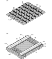
- FIG. 4 is a schematic external perspective view of a solid electrolytic capacitor.
- FIG. 4 is a schematic external perspective view of a solid electrolytic capacitor.
- FIG. 5 is a diagram schematically showing the flow of gas generated in a solid electrolytic capacitor.
- FIG. 6 is a flowchart showing an example of a schematic flow of the method for manufacturing a solid electrolytic capacitor according to the present embodiment.
- FIG. 7 is a flowchart showing an example of the process of forming a capacitor element sheet.
- FIG. 8(A) is an external perspective view showing the shape of the anode electrode of the capacitor element before singulation
- FIG. 8(B) is an external perspective view showing the shape of the capacitor element before singulation.
- FIG. 9 is an external view of the capacitor element in a multi-state state.
- FIG. 10 is an external perspective view showing the shape of the cathode electrode before singulation.
- FIG. 11 is a flowchart showing an example of a process for forming a sheet laminate.
- 12(A) and 12(B) are external perspective views showing a state in which a dam is formed on a capacitor element sheet.
- 13(A) and 13(B) are external perspective views showing a state in which a second dam and a first adhesive are formed on a capacitor element sheet.
- 14(A) and 14(B) are exploded perspective views showing a state in which a capacitor element sheet and a cathode electrode sheet are laminated.
- FIG. 15(A) is an exploded perspective view showing a laminated state of a capacitor element sheet and a cathode electrode sheet in a multi-state, and FIG.
- FIG. 15(B) is an exploded perspective view showing a laminated state of a capacitor element sheet and a cathode electrode sheet in a multi-state.
- FIG. 3 is an external perspective view showing a stacked state.
- FIG. 16 is a flowchart showing an example of the process of forming the first metal part and the second metal part.
- FIG. 17 is a side sectional view showing a schematic configuration of a solid electrolytic capacitor according to a second embodiment.
- FIG. 18 is a side sectional view showing a schematic configuration of a solid electrolytic capacitor in the third embodiment.
- FIG. 19 is a side sectional view showing a schematic configuration of a solid electrolytic capacitor in the fourth embodiment.
- FIG. 1 is a side sectional view showing the configuration of a solid electrolytic capacitor according to a first embodiment. Note that in FIG. 1, only the insulating resin and the external electrodes are hatched to make the diagram easier to read.
- FIG. 2(A) is a side sectional view showing the configuration of a set of a capacitor element and a cathode electrode before being separated into pieces.
- FIG. 2(B) is a side cross-sectional view showing the structure of the capacitor element before being separated into pieces.
- FIG. 2(C) is a side sectional view showing the configuration of a set of a capacitor element and a cathode electrode after being separated into pieces.
- the solid electrolytic capacitor 1 includes a capacitor element laminate 100, an insulating resin 50, metal films 61, 62, and an external Terminal electrodes 71 and 72 are provided.
- the capacitor element stack 100 includes a plurality of flat film-shaped capacitor elements 10 and a plurality of flat film-shaped cathode electrodes 20.
- the number of flat film capacitor elements 10 and the number of cathode electrodes is four, but the number is not limited to this.
- the cathode electrode 20 corresponds to the "cathode electrode foil" in the present invention.
- the metal films 61 and 62 correspond to the "first metal part" in the present invention
- the external terminal electrode 71 corresponds to the "second metal part” in the present invention.
- the metal film 61 serves as a collector electrode on the anode side of the solid electrolytic capacitor 1
- the metal film 62 serves as a collector electrode on the cathode side of the solid electrolytic capacitor 1 .
- the solid electrolytic capacitor 1 includes a first main surface 101 and a second main surface 102.
- the first main surface 101 and the second main surface 102 face each other.
- This second main surface 102 becomes the mounting surface side of the solid electrolytic capacitor 1.
- the capacitor element 10 includes a flat film-shaped anode electrode 11, a dielectric layer 12, and a CP layer (solid electrolyte layer) 13.
- the anode electrode 11 includes a large number of holes. In other words, the anode electrode 11 is in a porous state (porous body (porous portion)). The ratio of the thicknesses of the porous portion and the core metal portion on one side of the anode electrode 11 to the porous portion on the other side is approximately 1:1:1.
- Dielectric layer 12 covers the outer surface of anode electrode 11 . 2(A), FIG. 2(B), and FIG. 2(C) omit illustration of the detailed structure of the anode electrode 11, the dielectric layer 12 is schematically shown as a macroscopic surface of the anode electrode 11.
- the dielectric layer 12 covers not only the macroscopic surface of the anode electrode 11 but also the surfaces of many holes in the anode electrode 11 .
- the anode electrode 11 corresponds to the "anode electrode foil" in the present invention.
- the CP layer 13 covers the surface of the dielectric layer 12.
- the CP layer 13 is formed inside a frame-shaped first dam 14.
- the first dam 14 has insulation properties.
- the region in which the CP layer 13 is formed is regulated by the first dam 14 .
- the first dam 14 may not be formed in a frame shape. That is, the first dam 14 may be formed on one side, or may be formed on two sides having corners. Furthermore, the structure may be formed on two opposing sides in a plan view.
- the CP layer 13 has a laminated structure of an inner layer CP (inner solid electrolyte layer) 131 and an outer layer CP (outer solid electrolyte layer) 132.
- the inner layer CP131 is formed on the surface of the dielectric layer 12, and the outer layer CP132 is formed on the surface of the inner layer CP131.
- the plurality of capacitor elements 10 and the plurality of cathode electrodes 20 are alternately stacked so that their flat film surfaces are parallel and overlap in plan view.
- a second dam 30 and a first adhesive 40 are provided between adjacent capacitor elements 10 and cathode electrodes 20.
- the second dam 30 has insulation and adhesive properties.
- the first adhesive 40 has conductivity.
- the second dam 30 is formed in a frame shape along the outer periphery of the surface of the capacitor element 10 where the CP layer 13 and the cathode electrode 20 face each other. As shown in FIG. 2(B), the second dam 30 is formed to overlap the first dam 14. Note that the second dam 30 is made of an insulating material such as an insulating resin, for example.
- the first adhesive 40 is placed inside the frame defined by the second dam 30. Adjacent capacitor elements 10 and cathode electrodes 20 are bonded to each other by this first adhesive 40 .
- the first ends 10E1 of the plurality of capacitor elements 10 are at the same position when viewed from the side.
- the second ends 10E2 of the plurality of capacitor elements 10 are at the same position when viewed from the side.
- the first ends 20E1 of the plurality of cathode electrodes 20 are at the same position when viewed from the side.
- the second ends 20E2 of the plurality of cathode electrodes 20 are at the same position when viewed from the side.
- the same position includes unintentional variations during processing, and also includes the fact that the positions are not exactly the same.
- the first ends 10E1 of the plurality of capacitor elements 10 and the second ends 20E2 of the plurality of cathode electrodes 20 are arranged on the first end side of the capacitor element stack 100.
- the first ends 10E1 of the plurality of capacitor elements 10 protrude further outward than the second ends 20E2 of the plurality of cathode electrodes 20.
- the second ends 10E2 of the plurality of capacitor elements 10 and the first ends 20E1 of the plurality of cathode electrodes 20 are arranged on the second end side of the capacitor element stack 100.
- the first ends 20E1 of the plurality of cathode electrodes 20 protrude further outward than the second ends 10E2 of the plurality of capacitor elements 10.
- the capacitor element stack 100 is realized.
- the structure provided with the 1st adhesive 40 was demonstrated as an example.
- the CP layer 13 may be formed thicker, or a CP layer (solid electrolyte layer) containing a binder may be formed instead of the first adhesive 40. Even when the first adhesive 40 is omitted in this manner, a structure in which the capacitor element 10 and the cathode electrode 20 are bonded can be realized.
- the capacitor element stack 100 is sealed with an insulating resin 50. More specifically, the insulating resin 50 is applied to the capacitor element laminate except for the first ends 10E1 of the plurality of capacitor elements 10 (the first ends 10E1 of the anode electrodes 11) and the first ends 20E1 of the plurality of cathode electrodes 20. Cover 100.
- the metal film 61 covers the first end 10E1 of the anode electrode 11 and the outer surface of the insulating resin 50 on the first end 10E1 side. That is, the metal film 61 becomes a current collecting electrode on the anode side connected to the first end 10E1 side of the anode electrode 11 of the plurality of capacitor elements 10. Further, the external terminal electrode 71 is formed so as to be in contact with the metal film 61.
- the metal film 62 covers the first end 20E1 of the cathode electrode 20 and the outer surface of the insulating resin 50 on the first end 20E1 side. That is, the metal film 62 serves as a current collecting electrode on the cathode side connected to the first end 20E1 side of the cathode electrode 20 of the plurality of capacitor elements 10. Furthermore, the external terminal electrode 72 is formed so as to come into contact with the metal film 62.
- the solid electrolytic capacitor 1 is realized.
- FIG. 3A is a diagram schematically showing a case in which a metal film 61 is formed on the first end 10E1 side of the anode electrode 11 and a metal film 62 is formed on the first end 20E1 side of the cathode electrode 20.
- FIG. 3(B) is a diagram schematically showing the structure of FIG. 3(A) in which an external terminal electrode 71 and an external terminal electrode 72 are formed.
- FIG. 4 is an external perspective view showing an outline of the external terminal electrodes 71 and 72 formed on the capacitor element laminate 100.
- the metal film 61 is formed by spraying metal onto the first end 10E1 of the anode electrode 11 and the outer surface of the insulating resin 50 on the first end 10E1 side.
- the metal film 62 is formed by spraying metal onto the first end 20E1 of the cathode electrode 20 and the outer surface of the insulating resin 50 on the first end 20E1 side.
- the external terminal electrode 71 is formed so as to be in contact with the metal film 61. At this time, the external terminal electrode 71 covers a part of the mounting surface side of the metal film 61 (the second main surface 102 side of the capacitor element stack 100). The external terminal electrode 71 is opened on the side of the metal film 61 that faces the mounting surface. In other words, the external terminal electrode 71 is formed to have the opening 751 on the first main surface 101 side.
- the external terminal electrode 72 is formed so as to be in contact with the metal film 62. At this time, the external terminal electrode 72 covers a part of the mounting surface side of the metal film 62 (the second main surface 102 side of the capacitor element stack 100). The external terminal electrode 72 is opened on the side of the metal film 61 that faces the mounting surface. In other words, the external terminal electrode 72 is formed to have the opening 752 on the first main surface 101 side.
- the first pore diameter D1 of the metal films 61 and 62 is preferably larger than the second pore diameter D2 of the porous portion of the anode electrode 11. At this time, the first pore diameter D1 is the average pore diameter of the metal films 61 and 62, and the second pore diameter D2 is the average pore diameter of the anode electrode 11.
- the gas generated at the anode electrode 11 flows from the anode electrode 11 to the metal films 61 and 62. It becomes easier to flow in the direction of (see Figure 5).
- the external terminal electrode 71 is formed to have the opening 751 on the first main surface 101 side, gas flows in the direction of the opening 751.
- the external terminal electrode 72 is formed to have an opening 752 on the first main surface 101 side. Thus, gas flows in the direction of opening 752.
- gas generated at the anode electrode 11 during, for example, MSL reflow is discharged to the outside without remaining inside the solid electrolytic capacitor 1. That is, peeling and cracking due to gas generated within the solid electrolytic capacitor 1 is suppressed.
- FIG. 6 is a flowchart showing an example of a schematic flow of the method for manufacturing a solid electrolytic capacitor according to the present embodiment.
- a capacitor element sheet is formed (FIG. 6: S11).
- a plurality of capacitor elements 10 forming different solid electrolytic capacitors 1 are arranged on the capacitor element sheet.
- the capacitor element sheet and the cathode electrode sheet are laminated with the second dam 30 and the first adhesive 40 in between to form a sheet laminate (FIG. 6: S12).
- a plurality of cathode electrodes 20 forming different solid electrolytic capacitors 1 are arranged in the cathode electrode sheet.
- a structure in which a plurality of capacitor element laminates 100 are arranged in a plane is formed.
- the sheet laminate is one in which a plurality of capacitor element laminates 100 are arranged in a plane.
- the sheet stack is sealed with insulating resin 50 (FIG. 6: S13). Although details will be described later, at this time, a through hole penetrating from the upper surface to the lower surface of the sheet laminate is provided in the sheet laminate, and resin sealing is performed by compression molding.
- This sealing with the insulating resin 50 is performed in a multi-state state (a state in which a plurality of solid electrolytic capacitors 1 are arranged) before the solid electrolytic capacitors 1 are separated into individual pieces.
- the sheet stack sealed with the insulating resin 50 is cut into individual pieces (FIG. 6: S14). Specifically, cutting is performed along cutting lines E11, E12, S11, and S12 shown in FIG. 12(B), which will be described later. As a result, a plurality of solid electrolytic capacitors 1 (referred to as elements of solid electrolytic capacitors 1) in which no external electrodes are formed are formed. Thereafter, the element body of the solid electrolytic capacitor 1 is subjected to secondary sealing with an insulating resin 50.
- the side surface of the element body of the solid electrolytic capacitor 1 (the surface cut along the cutting lines S11 and S12 (the top surface, the bottom surface, the side surface different from the end surface where the anode electrode 11 and the cathode electrode 20 are exposed)) is insulated. It is covered by secondary sealing with a synthetic resin 50. Thereby, the anode electrode 11 and the cathode electrode 20 that are unnecessarily exposed during singulation are covered with the insulating resin 50.
- external electrodes consisting of metal films 61, 62 and external terminal electrodes 71, 72 are formed on the end face of the element body of the solid electrolytic capacitor 1 (FIG. 6: S15).
- FIG. 7 is a flowchart showing an example of the process of forming a capacitor element sheet.
- FIG. 8(A) is an external perspective view showing the shape of the anode electrode of the capacitor element before singulation
- FIG. 8(B) is an external perspective view showing the shape of the capacitor element before singulation.
- FIG. 9 is an external view in the multi-state.
- a chemical conversion treatment is performed on the anode electrode 11 to form the dielectric layer 12 (FIG. 7: S111).
- a large number of holes are formed on the surface of the anode electrode 11 by etching, and the vicinity of the surface of the anode electrode 11 is a porous body.
- the dielectric layer 12 covers the surface of the anode electrode 11 including the inner surface of the hole.
- an anode through hole is formed in the anode electrode 11 (FIG. 7: S112). More specifically, as shown in FIG. 8A, a plurality of cylindrical anode through holes 19C and groove-shaped anode through holes 19L are formed in the anode electrode 11.
- the plurality of cylindrical anode through-holes 19C and the groove-shaped anode through-holes 19L are arranged alternately along the direction in which the portions that will become the plurality of anode electrodes 11 are lined up.
- the plurality of cylindrical anode through holes 19C are formed at positions where the first end 10E1 of the anode electrode 11 is realized.
- the groove-shaped anode through hole 19L is formed at a position that straddles the portions that will become the adjacent anode electrodes 11 and at a position that realizes the second ends 10E2 of the adjacent anode electrodes 11.
- a CP layer (solid electrolyte layer) 13 is formed on the surface of the dielectric layer 12 (FIG. 7: S113). More specifically, as shown in FIG. 8(B), a first dam 14 having a frame-shaped opening is formed. Then, the CP layer 13 (a laminated structure of the inner layer CP131 and the outer layer CP132) is formed in the opening of the first dam 14.
- this structure is a multi-state structure in which a plurality of capacitor elements 10 (a structure consisting of an anode electrode 11, a dielectric layer 12, a CP layer 13, and a first dam 14) are arranged in two dimensions. It will be done.
- FIG. 10 is an external perspective view showing the shape of the cathode electrode before singulation.
- the cathode electrode 20 is formed with a plurality of cylindrical cathode through holes 29C and groove-shaped cathode through holes 29L.
- the plurality of cylindrical cathode through-holes 29C and the groove-shaped cathode through-holes 29L are arranged alternately along the direction in which the portions that will become the plurality of cathode electrodes 20 are lined up.
- a plurality of cylindrical cathode through holes 29C are formed at positions that realize the first end 20E1 of the cathode electrode 20.
- the groove-shaped cathode through hole 29L is formed at a position that straddles the portions that will become the adjacent cathode electrodes 20 and at a position that realizes the second ends 20E2 of the adjacent cathode electrodes 20.
- FIG. 11 is a flowchart showing an example of a process for forming a sheet laminate.
- FIG. 12 is an external perspective view showing a state in which a second dam is formed on a capacitor element sheet
- FIG. 12(A) shows a multi-state state
- FIG. 12(B) shows a portion of one capacitor element.
- FIG. 13 is an external perspective view showing a state in which a second dam and a first adhesive are formed on a capacitor element sheet
- FIG. 13(A) shows a multi-layer state
- FIG. 13(B) shows one capacitor element sheet. Shows the part.
- 14(A) and 14(B) are exploded perspective views showing a state in which a capacitor element sheet and a cathode electrode sheet are laminated.
- FIG. 14(A) and 14(B) show a portion corresponding to one solid electrolytic capacitor.
- FIG. 15(A) is an exploded perspective view showing a laminated state of a capacitor element sheet and a cathode electrode sheet in a multi-state
- FIG. 15(B) is an exploded perspective view showing a laminated state of a capacitor element sheet and a cathode electrode sheet in a multi-state.
- FIG. 3 is an external perspective view showing a stacked state.
- a second dam 30 is formed on the capacitor element sheet (FIG. 11: S121). More specifically, as shown in FIGS. 12(A) and 12(B), a second dam 30 having a frame-shaped opening is formed.
- the first adhesive 40 is placed inside the opening of the second dam 30 (FIG. 11: S122).
- capacitor element sheets and cathode electrode sheets are alternately laminated (FIG. 11: S123) . More specifically, the capacitor element sheet and the cathode electrode sheet are laminated so as to satisfy the following conditions.
- the plurality of cylindrical anode through holes 19C in the capacitor element sheet and the groove-shaped cathode through holes 29L in the cathode electrode sheet overlap.
- the groove-shaped anode through-hole 19L in the capacitor element sheet overlaps with the plurality of cylindrical cathode through-holes 29C in the cathode electrode sheet.
- the groove-shaped anode through-hole 19L in the capacitor element sheet and the groove-shaped cathode through-hole 29L in the cathode electrode sheet overlap.
- a plurality of these through holes are formed in accordance with the number of capacitor elements arranged in the sheet laminate. Therefore, a plurality of through holes are formed in the sheet stack, which penetrate from the top surface to the bottom surface of the sheet stack.
- step S124 the sheet laminate is heated and pressurized (FIG. 11: S124). Thereby, the capacitor element sheet and the cathode electrode sheet are adhered by the first adhesive 40, and a sheet laminate is formed. Note that, as described above, in the case of a structure in which the first adhesive 40 is omitted, step S122 can be omitted.
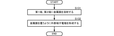
- FIG. 16 is a flowchart showing an example of a process for forming a metal film and an external terminal electrode.
- metal spraying is performed on the first end 10E1 of the anode electrode 11 and the outer surface of the insulating resin 50 on the first end 10E1 side.
- metal spraying is performed on the first end 20E1 of the cathode electrode 20 in the capacitor element laminate 100 and the outer surface of the insulating resin 50 on the first end 20E1 side (FIG. 16: S131).
- the metal film 61 is formed at the first end 10E1.
- a metal film 62 is formed on the first end 20E1.
- external terminal electrodes 71 and 72 are formed directly on metal films 61 and 62 by, for example, sputtering. Specifically, the external terminal electrode 71 is formed to cover the metal film 61. Similarly, an external terminal electrode 72 is formed to cover the metal film 62. At this time, the external terminal electrode 71 is formed to have an opening 751 toward the first main surface 101 side. Further, the external terminal electrode 72 is formed to have an opening 752 on the first main surface 101 side.
- the metal films 61 and 62 are formed by thermal spraying.
- the metal films 61 and 62 may be formed by a method other than thermal spraying.
- any configuration is sufficient as long as it includes at least the metal film 61 connected to the anode electrode 11 and the external terminal electrode 71, and the gas generated within the solid electrolytic capacitor 1 is discharged to the outside from the external electrode on the anode side. . That is, instead of the metal film 62 and the external terminal electrode 72, a configuration may be adopted in which an external electrode on the cathode side is formed by a conventionally used method.
- the external terminal electrodes 71 and 72 have a shape that covers the entire side surface of the solid electrolytic capacitor 1 (the first end 10E1 side of the anode electrode 11 and the first end 20E1 side of the cathode electrode 20).
- the external terminal electrodes 71 and 72 may have any shape as long as they can expose a portion of the metal films 61 and 62 and release the gas generated within the solid electrolytic capacitor 1 to the outside.
- the shape that covers the whole includes unintentional variations during processing, and strictly speaking also includes the shape that does not cover the whole.
- the opening 751 of the external terminal electrode 71 and the opening 752 of the external terminal electrode 72 are formed on the first main surface 101 side.
- the openings 751 and 752 are not limited to the first main surface 101 side, and the positions where they are formed are not limited as long as there is no problem with mounting.
- the openings 751 and 752 may be located at any position, except where the openings 751 and 752 are covered with solder or conductive adhesive during mounting, and gas generated within the solid electrolytic capacitor 1 cannot be released to the outside. good.
- the openings 751 and 752 only need to have a size, shape, and number of openings that allow gas to be released.
- FIG. 17 is a side sectional view showing a schematic configuration of a solid electrolytic capacitor in the second embodiment.
- a solid electrolytic capacitor 1A according to the second embodiment differs from the solid electrolytic capacitor 1 according to the first embodiment in that it includes a conductive resin layer.
- the other configuration of the solid electrolytic capacitor 1A is the same as that of the solid electrolytic capacitor 1, and the explanation of the similar parts will be omitted.
- FIG. 17 an example is shown using FIG. 17 in which external terminal electrodes 71 and 72 are formed in a state where they are already formed on metal films 61 and 62 using a conductive adhesive.
- the metal film 61 is formed by performing metal spraying on the first end 10E1 of the anode electrode 11 and the outer surface of the insulating resin 50 on the first end 10E1 side.
- a conductive resin layer 81 is formed to cover the surface (outer surface side) of this metal film 61 facing the first end 10E1.
- external terminal electrodes 71 are formed to cover conductive resin layer 81.
- the metal film 62 is formed by performing metal spraying on the first end 20E1 of the cathode electrode 20 and the outer surface of the first end 20E1 side of the insulating resin 50.
- a conductive resin layer 82 is formed to cover the surface (outer surface side) of this metal film 62 facing the first end 20E1.
- external terminal electrodes 72 are formed to cover the conductive resin layer 82.
- a structure in which a metal film 62 and an external terminal electrode 72 are formed is shown.
- any configuration may be used as long as it includes at least the metal film 61 connected to the anode electrode 11 and the external terminal electrode 71, and the gas generated within the solid electrolytic capacitor 1 is discharged to the outside from the external electrode on the anode side. That is, instead of the metal film 62 and the external terminal electrode 72, a configuration may be adopted in which an external electrode on the cathode side is formed by a conventionally used method.
- the adhesive strength between the metal film 61 and the external terminal electrode 71 is increased. Similarly, the adhesive strength between the metal film 62 and the external terminal electrode 72 increases.
- the conductive resin layer 82 can suppress peeling between the metal film 62 and the external terminal electrode 72 due to a difference in linear expansion coefficient.
- FIG. 18 is a side sectional view showing a schematic configuration of a solid electrolytic capacitor in the third embodiment.
- a solid electrolytic capacitor 1B according to the third embodiment differs from the solid electrolytic capacitor 1 according to the first embodiment in that it includes a non-conductive resin layer.
- the other configuration of the solid electrolytic capacitor 1B is the same as that of the solid electrolytic capacitor 1, and the explanation of the similar parts will be omitted.
- a metal film 61 is formed by performing metal spraying on the first end 10E1 of the anode electrode 11 and the outer surface of the first end 10E1 side of the insulating resin 50.
- a non-conductive resin layer 91 is formed to cover the surface (outer surface side) of this metal film 61 facing the first end 10E1. At this time, a part of the surface of the metal film 61 has a portion that is not covered with the non-conductive resin layer 91.
- external terminal electrodes 71 are formed to cover non-conductive resin layer 91.
- the shape of the non-conductive resin layer 91 is not limited as long as the metal film 61 and the external terminal electrode 71 can be used as an anode electrode.
- the metal film 62 is formed by performing metal spraying on the first end 20E1 of the cathode electrode 20 and the outer surface of the first end 20E1 side of the insulating resin 50.
- a non-conductive resin layer 92 is formed to cover the surface (outer surface side) of this metal film 62 facing the first end 20E1. At this time, a part of the surface of the metal film 62 has a portion that is not covered with the non-conductive resin layer 92.
- external terminal electrodes 72 are formed to cover non-conductive resin layer 92.
- the shape of the non-conductive resin layer 92 is not limited as long as the metal film 62 and the external terminal electrode 72 can be used as a cathode electrode.
- the adhesive strength between the metal film 61 and the external terminal electrode 71 is increased. Similarly, the adhesive strength between the metal film 62 and the external terminal electrode 72 increases.
- FIG. 19 is a side sectional view showing a schematic configuration of a solid electrolytic capacitor in the fourth embodiment.
- the solid electrolytic capacitor 1C according to the fourth embodiment differs from the solid electrolytic capacitor 1A according to the second embodiment in the configuration of the conductive resin layer.
- the other configuration of the solid electrolytic capacitor 1C is the same as that of the solid electrolytic capacitor 1A, and the description of the similar parts will be omitted.
- the conductive resin layer 81 has penetrated into the metal film 61. More specifically, the conductive resin layer 81 penetrates into the metal film 61 to a thickness that is half the thickness T61 (T61/2). However, the half thickness includes unintended variations during processing, and strictly speaking, includes the fact that the conductive resin layer 81 is not half the thickness T61 of the metal film 61.
- Capacitor element 10 (Explanation of an example of specific materials, etc. of each component of solid electrolytic capacitor 1) (Capacitor element 10)
- the capacitor element 10 is realized using, for example, the following materials and thicknesses.
- the anode electrode 11 is made of, for example, a single metal such as aluminum, tantalum, niobium, titanium, zirconium, or magnesium, or an alloy containing these metals. Note that the anode electrode 11 is preferably made of aluminum or an aluminum alloy. The anode electrode 11 may be any valve metal as long as it exhibits a so-called valve action.
- the anode electrode 11 has a flat plate shape, and the thickness of the core part of the anode electrode 11 (the central part where the pores of the porous body do not reach) is preferably 5 ⁇ m or more and 100 ⁇ m or less.
- the thickness (thickness of one side) of the porous portion (the portion of the porous body in which pores are formed) is preferably 5 ⁇ m or more and 200 ⁇ m or less.
- the dielectric layer 12 is preferably made of an oxide film of the anode electrode 11.
- the dielectric layer 12 is formed by oxidizing it in an aqueous solution containing boric acid, phosphoric acid, adipic acid, or their sodium or ammonium salts.
- the thickness of the dielectric layer 12 is preferably 1 nm or more and 100 nm or less.
- the inner layer CP131 is made of, for example, a conductive polymer having a backbone of pyrroles, thiophenes, anilines, etc., or PEDOT [poly(3,4-ethylenedioxythiophene)], which is a conductive polymer having a backbone of thiophenes. It may also be a layer of PEDOT:PSS, which is realized by a method such as PEDOT:PSS and is composited with polystyrene sulfonic acid (PSS) as a dopant.
- PEDOT poly(3,4-ethylenedioxythiophene)
- the inner layer CP131 is formed by forming a polymer film of poly(3,4-ethylenedioxythiophene) or the like on the surface of the dielectric layer 12 using, for example, a treatment liquid containing a monomer such as 3,4-ethylenedioxythiophene. It is formed by applying a dispersion of a polymer such as poly(3,4-ethylenedioxythiophene) to the surface of the dielectric part and drying it.
- the thickness of the outer layer CP132 is preferably 2 ⁇ m or more and 20 ⁇ m or less.
- the material of the outer layer CP132 is the same as that of the inner layer CP131.
- the first adhesive 40 may be, for example, a mixture of an insulating resin such as an epoxy resin or a phenol resin, and conductive particles such as carbon or silver.
- the cathode electrode 20 is made of, for example, aluminum, titanium, copper, silver, or the like.
- the thickness of the cathode electrode 20 is, for example, thinner than or approximately the same as the thickness of the anode electrode 11. Note that the thickness of the cathode electrode 20 is preferably as thin as possible, and is about 5 ⁇ m to 50 ⁇ m, preferably about 30 ⁇ m.
- the insulating resin 50 may contain filler.
- the resin include epoxy resins, phenol resins, polyimide resins, silicone resins, polyamide resins, and liquid crystal polymers.
- the filler for example, insulating oxide particles such as silica particles, alumina particles, titania particles, and zirconia particles are preferable.
- the maximum diameter of the filler is preferably 30 ⁇ m or more and 40 ⁇ m or less, for example. For example, it is more preferable to use a material containing silica particles in solid epoxy resin and phenol resin.
- the metal films 61 and 62 are preferably formed of a metal that can be sprayed.
- the first pore diameter D1 of the metal films 61 and 62 can be easily made larger than the second pore diameter D2 of the porous portion of the anode electrode 11.
- a relatively large metal in a molten or semi-molten state is applied to the first end 10E1 of the anode electrode 11 and the outer surface of the first end 10E1 side of the insulating resin 50. This is thought to be because pores are likely to be formed when the particles arrive and the large metal particles are cooled and solidified. The same applies to the metal film 62.
- the external terminal electrodes 71 and 72 may be made of a material that has high solder wettability with respect to the surfaces of the external terminal electrodes 71 and 72.
- the conductive resin layers 81 and 82 are thermosetting resins that have conductivity.
- thermosetting resins that have conductivity.
- phenol resin or the like may be used.
- the non-conductive resin layers 91 and 92 are made of non-conductive thermosetting resin.
- epoxy resin or the like may be used.
- First adhesive 50 ...Insulating resin 61, 62...Metal film 71, 72...External terminal electrodes 81, 82...Conductive resin layer 91, 92...Non-conductive resin layer 100...Capacitor element laminate 101...First main Surface 102...Second main surface 751, 752...Opening
Landscapes
- Engineering & Computer Science (AREA)
- Power Engineering (AREA)
- Microelectronics & Electronic Packaging (AREA)
- Manufacturing & Machinery (AREA)
- Fixed Capacitors And Capacitor Manufacturing Machines (AREA)
Priority Applications (3)
| Application Number | Priority Date | Filing Date | Title |
|---|---|---|---|
| CN202380057486.XA CN119631151A (zh) | 2022-08-02 | 2023-07-28 | 固体电解电容器 |
| JP2024539123A JPWO2024029458A1 (https=) | 2022-08-02 | 2023-07-28 | |
| US19/038,972 US20250174412A1 (en) | 2022-08-02 | 2025-01-28 | Solid electrolytic capacitor |
Applications Claiming Priority (2)
| Application Number | Priority Date | Filing Date | Title |
|---|---|---|---|
| JP2022-123086 | 2022-08-02 | ||
| JP2022123086 | 2022-08-02 |
Related Child Applications (1)
| Application Number | Title | Priority Date | Filing Date |
|---|---|---|---|
| US19/038,972 Continuation US20250174412A1 (en) | 2022-08-02 | 2025-01-28 | Solid electrolytic capacitor |
Publications (1)
| Publication Number | Publication Date |
|---|---|
| WO2024029458A1 true WO2024029458A1 (ja) | 2024-02-08 |
Family
ID=89849041
Family Applications (1)
| Application Number | Title | Priority Date | Filing Date |
|---|---|---|---|
| PCT/JP2023/027731 Ceased WO2024029458A1 (ja) | 2022-08-02 | 2023-07-28 | 固体電解コンデンサ |
Country Status (4)
| Country | Link |
|---|---|
| US (1) | US20250174412A1 (https=) |
| JP (1) | JPWO2024029458A1 (https=) |
| CN (1) | CN119631151A (https=) |
| WO (1) | WO2024029458A1 (https=) |
Citations (3)
| Publication number | Priority date | Publication date | Assignee | Title |
|---|---|---|---|---|
| JPH04188814A (ja) * | 1990-11-22 | 1992-07-07 | Matsushita Electric Ind Co Ltd | 積層型固体電解コンデンサ |
| JP2005026257A (ja) * | 2003-06-30 | 2005-01-27 | Matsushita Electric Ind Co Ltd | 固体電解コンデンサおよびその製造方法 |
| WO2021140894A1 (ja) * | 2020-01-09 | 2021-07-15 | 株式会社村田製作所 | 電解コンデンサ及び電解コンデンサの製造方法 |
Family Cites Families (6)
| Publication number | Priority date | Publication date | Assignee | Title |
|---|---|---|---|---|
| JP2001057321A (ja) * | 1999-08-18 | 2001-02-27 | Nec Corp | チップ型固体電解コンデンサ |
| JP5176919B2 (ja) * | 2008-12-09 | 2013-04-03 | 株式会社デンソー | コンデンサ単素子、及びコンデンサモジュール |
| JP5466722B2 (ja) * | 2011-04-15 | 2014-04-09 | Necトーキン株式会社 | 固体電解コンデンサ |
| JP2013171989A (ja) * | 2012-02-21 | 2013-09-02 | Toyota Motor Corp | コンデンサとその製造方法 |
| JP2021034458A (ja) * | 2019-08-21 | 2021-03-01 | 株式会社村田製作所 | 積層セラミック電子部品 |
| JP2022067931A (ja) * | 2020-10-21 | 2022-05-09 | Tdk株式会社 | 電子部品 |
-
2023
- 2023-07-28 CN CN202380057486.XA patent/CN119631151A/zh active Pending
- 2023-07-28 JP JP2024539123A patent/JPWO2024029458A1/ja active Pending
- 2023-07-28 WO PCT/JP2023/027731 patent/WO2024029458A1/ja not_active Ceased
-
2025
- 2025-01-28 US US19/038,972 patent/US20250174412A1/en active Pending
Patent Citations (3)
| Publication number | Priority date | Publication date | Assignee | Title |
|---|---|---|---|---|
| JPH04188814A (ja) * | 1990-11-22 | 1992-07-07 | Matsushita Electric Ind Co Ltd | 積層型固体電解コンデンサ |
| JP2005026257A (ja) * | 2003-06-30 | 2005-01-27 | Matsushita Electric Ind Co Ltd | 固体電解コンデンサおよびその製造方法 |
| WO2021140894A1 (ja) * | 2020-01-09 | 2021-07-15 | 株式会社村田製作所 | 電解コンデンサ及び電解コンデンサの製造方法 |
Also Published As
| Publication number | Publication date |
|---|---|
| JPWO2024029458A1 (https=) | 2024-02-08 |
| CN119631151A (zh) | 2025-03-14 |
| US20250174412A1 (en) | 2025-05-29 |
Similar Documents
| Publication | Publication Date | Title |
|---|---|---|
| KR102242756B1 (ko) | 고체 전해 콘덴서의 제조 방법 및 고체 전해 콘덴서 | |
| JP2023053310A (ja) | 電解コンデンサおよびその製造方法 | |
| JP7408288B2 (ja) | 固体電解コンデンサ | |
| US10032567B2 (en) | Solid-state electrolytic capacitor manufacturing method and solid-state electrolytic capacitor | |
| CN111755253B (zh) | 固体电解电容器的制造方法 | |
| WO2019087692A1 (ja) | 電解コンデンサおよびその製造方法 | |
| WO2022163645A1 (ja) | 電解コンデンサ | |
| JP2020102651A (ja) | 固体電解コンデンサ | |
| WO2022163644A1 (ja) | 電解コンデンサ | |
| WO2024029458A1 (ja) | 固体電解コンデンサ | |
| JP7619541B1 (ja) | コンデンサ素子 | |
| JP7501541B2 (ja) | 固体電解コンデンサ | |
| WO2019156120A1 (ja) | 電解コンデンサ | |
| JP7419791B2 (ja) | 固体電解コンデンサ | |
| CN223155823U (zh) | 固体电解电容器 | |
| WO2026070017A1 (ja) | 固体電解コンデンサおよび固体電解コンデンサの製造方法 | |
| JP7806906B2 (ja) | 固体電解コンデンサ、および、固体電解コンデンサの製造方法 | |
| JP7750382B2 (ja) | 固体電解コンデンサの製造方法 | |
| JP2023181685A (ja) | 固体電解コンデンサ | |
| WO2023243626A1 (ja) | 電解コンデンサ | |
| WO2025105152A1 (ja) | 固体電解コンデンサ、および固体電解コンデンサの製造方法 | |
| WO2012002359A1 (ja) | 蓄電デバイスとその製造方法 | |
| WO2024090047A1 (ja) | 固体電解コンデンサ | |
| WO2024135309A1 (ja) | 固体電解コンデンサ | |
| WO2026048925A1 (ja) | コンデンサ素子 |
Legal Events
| Date | Code | Title | Description |
|---|---|---|---|
| 121 | Ep: the epo has been informed by wipo that ep was designated in this application |
Ref document number: 23850013 Country of ref document: EP Kind code of ref document: A1 |
|
| WWE | Wipo information: entry into national phase |
Ref document number: 2024539123 Country of ref document: JP |
|
| WWE | Wipo information: entry into national phase |
Ref document number: 202380057486.X Country of ref document: CN |
|
| NENP | Non-entry into the national phase |
Ref country code: DE |
|
| WWP | Wipo information: published in national office |
Ref document number: 202380057486.X Country of ref document: CN |
|
| 122 | Ep: pct application non-entry in european phase |
Ref document number: 23850013 Country of ref document: EP Kind code of ref document: A1 |