WO2024090047A1 - 固体電解コンデンサ - Google Patents
固体電解コンデンサ Download PDFInfo
- Publication number
- WO2024090047A1 WO2024090047A1 PCT/JP2023/032476 JP2023032476W WO2024090047A1 WO 2024090047 A1 WO2024090047 A1 WO 2024090047A1 JP 2023032476 W JP2023032476 W JP 2023032476W WO 2024090047 A1 WO2024090047 A1 WO 2024090047A1
- Authority
- WO
- WIPO (PCT)
- Prior art keywords
- capacitor element
- capacitor
- solid electrolytic
- electrode
- electrolytic capacitor
- Prior art date
Links
- 239000003990 capacitor Substances 0.000 title claims abstract description 433
- 239000007787 solid Substances 0.000 title claims abstract description 95
- 239000011347 resin Substances 0.000 claims abstract description 30
- 229920005989 resin Polymers 0.000 claims abstract description 30
- 239000011888 foil Substances 0.000 claims abstract description 18
- 239000007784 solid electrolyte Substances 0.000 claims abstract description 14
- 238000010030 laminating Methods 0.000 claims abstract 2
- 239000012528 membrane Substances 0.000 claims 1
- 239000013256 coordination polymer Substances 0.000 description 25
- 238000000034 method Methods 0.000 description 12
- 238000004519 manufacturing process Methods 0.000 description 9
- 229910052751 metal Inorganic materials 0.000 description 8
- 239000002184 metal Substances 0.000 description 8
- -1 poly(3,4-ethylenedioxythiophene) Polymers 0.000 description 6
- 239000000463 material Substances 0.000 description 5
- OKTJSMMVPCPJKN-UHFFFAOYSA-N Carbon Chemical compound [C] OKTJSMMVPCPJKN-UHFFFAOYSA-N 0.000 description 4
- 229920001609 Poly(3,4-ethylenedioxythiophene) Polymers 0.000 description 4
- 229910052799 carbon Inorganic materials 0.000 description 4
- 238000010586 diagram Methods 0.000 description 4
- 239000002245 particle Substances 0.000 description 4
- 229910052782 aluminium Inorganic materials 0.000 description 3
- XAGFODPZIPBFFR-UHFFFAOYSA-N aluminium Chemical compound [Al] XAGFODPZIPBFFR-UHFFFAOYSA-N 0.000 description 3
- 229920001940 conductive polymer Polymers 0.000 description 3
- 239000000945 filler Substances 0.000 description 3
- 238000007789 sealing Methods 0.000 description 3
- 229930192474 thiophene Chemical class 0.000 description 3
- 150000003577 thiophenes Chemical class 0.000 description 3
- NBIIXXVUZAFLBC-UHFFFAOYSA-N Phosphoric acid Chemical compound OP(O)(O)=O NBIIXXVUZAFLBC-UHFFFAOYSA-N 0.000 description 2
- VYPSYNLAJGMNEJ-UHFFFAOYSA-N Silicium dioxide Chemical compound O=[Si]=O VYPSYNLAJGMNEJ-UHFFFAOYSA-N 0.000 description 2
- GWEVSGVZZGPLCZ-UHFFFAOYSA-N Titan oxide Chemical compound O=[Ti]=O GWEVSGVZZGPLCZ-UHFFFAOYSA-N 0.000 description 2
- MCMNRKCIXSYSNV-UHFFFAOYSA-N Zirconium dioxide Chemical compound O=[Zr]=O MCMNRKCIXSYSNV-UHFFFAOYSA-N 0.000 description 2
- 239000000853 adhesive Substances 0.000 description 2
- 230000001070 adhesive effect Effects 0.000 description 2
- WNLRTRBMVRJNCN-UHFFFAOYSA-N adipic acid Chemical compound OC(=O)CCCCC(O)=O WNLRTRBMVRJNCN-UHFFFAOYSA-N 0.000 description 2
- 230000015572 biosynthetic process Effects 0.000 description 2
- 239000003822 epoxy resin Substances 0.000 description 2
- 239000005011 phenolic resin Substances 0.000 description 2
- 229920000172 poly(styrenesulfonic acid) Polymers 0.000 description 2
- 229920000647 polyepoxide Polymers 0.000 description 2
- 229940005642 polystyrene sulfonic acid Drugs 0.000 description 2
- 239000011148 porous material Substances 0.000 description 2
- 239000000758 substrate Substances 0.000 description 2
- GKWLILHTTGWKLQ-UHFFFAOYSA-N 2,3-dihydrothieno[3,4-b][1,4]dioxine Chemical compound O1CCOC2=CSC=C21 GKWLILHTTGWKLQ-UHFFFAOYSA-N 0.000 description 1
- 229910000838 Al alloy Inorganic materials 0.000 description 1
- RYGMFSIKBFXOCR-UHFFFAOYSA-N Copper Chemical compound [Cu] RYGMFSIKBFXOCR-UHFFFAOYSA-N 0.000 description 1
- 229920000106 Liquid crystal polymer Polymers 0.000 description 1
- 239000004977 Liquid-crystal polymers (LCPs) Substances 0.000 description 1
- FYYHWMGAXLPEAU-UHFFFAOYSA-N Magnesium Chemical compound [Mg] FYYHWMGAXLPEAU-UHFFFAOYSA-N 0.000 description 1
- 229920000144 PEDOT:PSS Polymers 0.000 description 1
- RTAQQCXQSZGOHL-UHFFFAOYSA-N Titanium Chemical compound [Ti] RTAQQCXQSZGOHL-UHFFFAOYSA-N 0.000 description 1
- QCWXUUIWCKQGHC-UHFFFAOYSA-N Zirconium Chemical compound [Zr] QCWXUUIWCKQGHC-UHFFFAOYSA-N 0.000 description 1
- 239000001361 adipic acid Substances 0.000 description 1
- 235000011037 adipic acid Nutrition 0.000 description 1
- 229910045601 alloy Inorganic materials 0.000 description 1
- 239000000956 alloy Substances 0.000 description 1
- PNEYBMLMFCGWSK-UHFFFAOYSA-N aluminium oxide Inorganic materials [O-2].[O-2].[O-2].[Al+3].[Al+3] PNEYBMLMFCGWSK-UHFFFAOYSA-N 0.000 description 1
- 229910000147 aluminium phosphate Inorganic materials 0.000 description 1
- 150000003863 ammonium salts Chemical class 0.000 description 1
- 150000001448 anilines Chemical class 0.000 description 1
- 239000007864 aqueous solution Substances 0.000 description 1
- KGBXLFKZBHKPEV-UHFFFAOYSA-N boric acid Chemical compound OB(O)O KGBXLFKZBHKPEV-UHFFFAOYSA-N 0.000 description 1
- 239000004327 boric acid Substances 0.000 description 1
- 230000015556 catabolic process Effects 0.000 description 1
- 238000006243 chemical reaction Methods 0.000 description 1
- 238000000748 compression moulding Methods 0.000 description 1
- 229910052802 copper Inorganic materials 0.000 description 1
- 239000010949 copper Substances 0.000 description 1
- 239000006185 dispersion Substances 0.000 description 1
- 239000002019 doping agent Substances 0.000 description 1
- 238000001035 drying Methods 0.000 description 1
- 238000005530 etching Methods 0.000 description 1
- 239000007788 liquid Substances 0.000 description 1
- 229910052749 magnesium Inorganic materials 0.000 description 1
- 239000011777 magnesium Substances 0.000 description 1
- 150000002739 metals Chemical class 0.000 description 1
- 239000000178 monomer Substances 0.000 description 1
- 229910052758 niobium Inorganic materials 0.000 description 1
- 239000010955 niobium Substances 0.000 description 1
- GUCVJGMIXFAOAE-UHFFFAOYSA-N niobium atom Chemical compound [Nb] GUCVJGMIXFAOAE-UHFFFAOYSA-N 0.000 description 1
- 230000001590 oxidative effect Effects 0.000 description 1
- 229920006122 polyamide resin Polymers 0.000 description 1
- 229920001721 polyimide Polymers 0.000 description 1
- 239000009719 polyimide resin Substances 0.000 description 1
- 229920000642 polymer Polymers 0.000 description 1
- 229920006254 polymer film Polymers 0.000 description 1
- 150000003233 pyrroles Chemical class 0.000 description 1
- 238000007652 sheet-forming process Methods 0.000 description 1
- 229920002050 silicone resin Polymers 0.000 description 1
- 159000000000 sodium salts Chemical class 0.000 description 1
- 239000000126 substance Substances 0.000 description 1
- 229910052715 tantalum Inorganic materials 0.000 description 1
- GUVRBAGPIYLISA-UHFFFAOYSA-N tantalum atom Chemical compound [Ta] GUVRBAGPIYLISA-UHFFFAOYSA-N 0.000 description 1
- 239000010936 titanium Substances 0.000 description 1
- 229910052719 titanium Inorganic materials 0.000 description 1
- 229910052726 zirconium Inorganic materials 0.000 description 1
Images


Definitions
- the present invention relates to a solid electrolytic capacitor that comprises a laminate of multiple capacitor elements.
- Patent Document 1 describes a method for manufacturing a solid electrolytic capacitor and a solid electrolytic capacitor.
- the solid electrolytic capacitor described in Patent Document 1 comprises multiple flat-film capacitor elements and multiple metal foils (cathodes).
- the flat-film capacitor elements comprise a foil-shaped valve metal substrate (anode), a porous portion of the valve metal substrate and a dielectric layer formed on the surface, and a solid electrolyte layer formed on the surface of the dielectric layer.
- the porous portion of the capacitor element of Patent Document 1 is impregnated with insulating resin (mask member). Furthermore, an insulating adhesive is formed in a frame shape in this insulating resin. A solid electrolyte layer is formed within the frame of the insulating adhesive. The flat film-shaped capacitor elements and metal foil are layered alternately. This forms an element stack.
- the object of the present invention is therefore to provide a solid electrolytic capacitor that has high voltage resistance, is compact, and is easy to manufacture.
- the solid electrolytic capacitor of the present invention comprises a sheet laminate formed by stacking a first capacitor element and a second capacitor element, each of which has a dielectric layer formed on the surface of a flat electrode foil and a solid electrolyte layer formed on the surface of the dielectric layer, and an insulating resin that seals the sheet laminate.
- the first pole is formed by drawing out the electrode foil of the first capacitor element from a first end face of the sheet laminate
- the second pole is formed by drawing out the electrode foil of the second capacitor element from a second end face that faces the first end face of the sheet laminate.
- This configuration makes it easy to form a non-polar solid electrolytic capacitor.
- each capacitor element is connected in series, a high breakdown voltage can be achieved.
- This invention makes it possible to provide a solid electrolytic capacitor that has high voltage resistance, is compact, and is easy to manufacture.
- FIG. 1 is a side cross-sectional view showing the configuration of the solid electrolytic capacitor according to the first embodiment.
- FIG. 2A is a side cross-sectional view showing the configuration of a capacitor element before being divided into individual pieces
- FIG. 2B is a side cross-sectional view showing an outline of a structure in which the capacitor elements are stacked.
- FIG. 3 is a circuit diagram of the solid electrolytic capacitor according to the first embodiment.
- FIG. 4 is a flowchart showing an example of a schematic flow of the method for manufacturing the solid electrolytic capacitor according to the first embodiment.
- FIG. 5 is a flow chart showing an example of a process for forming a capacitor element sheet.
- FIG. 6A is an external perspective view showing the shape of a capacitor element before being singulated, and FIG.
- FIG. 6B is an external perspective view showing the shape of a capacitor element before being singulated.
- FIG. 7 is an external view of the capacitor element in a multi-connected state.
- FIG. 8 is a flow chart showing an example of a process for forming a sheet laminate.
- FIG. 9 is an exploded perspective view of the sheet stack.
- FIG. 10 is an exploded perspective view of a set of capacitor elements being stacked.
- FIG. 11 is a side cross-sectional view showing the configuration of the solid electrolytic capacitor according to the second embodiment.
- FIG. 12 is a side cross-sectional view showing an outline of a structure in which capacitor elements according to the second embodiment are stacked.
- FIG. 13A is an external perspective view showing the shape of the third capacitor element before being singulated, and FIG.
- FIG. 13B is an external perspective view showing the shape of the third capacitor element before being singulated.
- FIG. 14 is a circuit diagram of the solid electrolytic capacitor according to the second embodiment.
- FIG. 15 is a side cross-sectional view showing the configuration of the solid electrolytic capacitor according to the third embodiment.
- FIG. 16 is a side cross-sectional view showing an outline of a structure in which capacitor elements according to the third embodiment are stacked.
- FIG. 17 is a side cross-sectional view showing an outline of a structure in which capacitor elements according to the fourth embodiment are stacked.
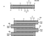
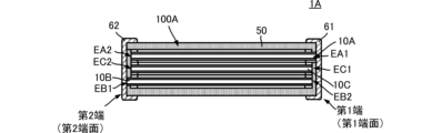
- Fig. 1 is a side cross-sectional view showing the configuration of a solid electrolytic capacitor according to a first embodiment. In Fig. 1, only the insulating resin and the external electrodes are hatched to make the drawing easier to see.
- Fig. 2(A) is a side cross-sectional view showing the configuration of a capacitor element before being divided into individual pieces, and Fig. 2(B) is a side cross-sectional view showing an outline of a structure in which the capacitor elements are stacked.
- the solid electrolytic capacitor 1 comprises a capacitor element laminate 100, insulating resin 50, an external electrode 61 and an external electrode 62.
- the capacitor element laminate 100 comprises a plurality of flat film-shaped first capacitor elements 10A and a plurality of second capacitor elements 10B. Note that in Figure 1, the number (number) of flat film-shaped first capacitor elements 10A and second capacitor elements 10B is two each, but this is not limited to this.
- the external electrode 61 corresponds to the "first external electrode” in the present invention, and the external electrode 62 corresponds to the "second external electrode” in the present invention.
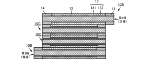
- the first capacitor element 10A and the second capacitor element 10B include a flat film-like electrode 11, a dielectric layer 12, and a CP layer (solid electrolyte layer) 13.
- the electrode 11 corresponds to the "electrode foil" of the present invention.
- the electrode 11 has many holes. In other words, the electrode 11 is in a porous state (porous body). The ratio of the thickness of the porous portion on one side of the electrode 11 to the thickness of the core metal portion and the porous portion on the other side is about 1:1:1.
- the dielectric layer 12 covers the outer surface of the electrode 11. Since detailed structure of the electrode 11 is omitted in Fig. 2(A) and Fig. 2(B), the dielectric layer 12 is illustrated as if it were covering the macroscopic surface of the electrode 11. In reality, the dielectric layer 12 covers not only the macroscopic surface of the electrode 11 but also the surfaces of the many holes in the electrode 11.
- the CP layer 13 covers the surface of the dielectric layer 12.
- the CP layer 13 is formed inside a frame-shaped first dam 14.
- the first dam 14 has insulating properties.
- the first dam 14 restricts the formation area of the CP layer 13.
- the first dam 14 is formed in a frame shape, and then the CP layer 13 is formed inside the first dam 14.
- the first dam 14 does not have to be formed in a frame shape. That is, the first dam 14 may be formed on one side, or on two sides having a corner. Furthermore, the first dam 14 may be formed on two sides that are opposite to each other in a plan view.
- the CP layer can be formed only on the surface of the dielectric layer 12, the first dam 14 may be omitted.
- the CP layer 13 has a laminated structure of an inner layer CP (inner layer solid electrolyte layer) 131 and an outer layer CP (outer layer solid electrolyte layer) 132.
- the inner layer CP 131 is formed on the surface of the dielectric layer 12, and the outer layer CP 132 is formed on the surface of the inner layer CP 131.
- the multiple first capacitor elements 10A and the multiple second capacitor elements 10B are alternately stacked so that their flat film surfaces are parallel and overlap when viewed in a plane.
- An outer layer CP (outer solid electrolyte layer) 132 is disposed between the first capacitor element 10A and the second capacitor element 10B.
- the first capacitor element 10A and the second capacitor element 10B are bonded together using this outer layer CP 132.
- a carbon layer may be formed between the first capacitor element 10A and the second capacitor element 10B so as to abut against the outer layer CP132.
- the adhesion strength between the first capacitor element 10A and the second capacitor element 10B can be improved, and low resistance can be achieved.
- a second dam (not shown) is present to restrict the formation area of the carbon layer.
- each of the first capacitor element 10A and the second capacitor element 10B has an outer layer CP132, but it is also possible to omit one of the outer layers CP132 at the surface where the first capacitor element 10A and the second capacitor element 10B abut. In this case, the thickness of the solid electrolytic capacitor 1 can be made thinner by the amount of the omitted outer layer CP132.
- the first ends EA1 of the multiple first capacitor elements 10A are at approximately the same position in side view.
- the second ends EA2 of the multiple first capacitor elements 10A are at approximately the same position in side view.
- the first ends EB1 of the multiple second capacitor elements 10B are at approximately the same position in side view.
- the second ends EB2 of the multiple second capacitor elements 10B are at approximately the same position in side view.
- the first ends EA1 of the multiple first capacitor elements 10A and the second ends EB2 of the multiple second capacitor elements 10B are arranged on the first end side of the capacitor element stack 100.
- the first ends EA1 of the multiple first capacitor elements 10A protrude outward further than the second ends EB2 of the multiple second capacitor elements 10B.
- the first end EA1 of the first capacitor element 10A corresponds to the "first pole" of the present invention. This first end EA1 is part of the first end surface of the capacitor element stack 100.
- the first ends EB1 of the multiple second capacitor elements 10B and the second ends EA2 of the multiple first capacitor elements 10A are arranged on the second end side of the capacitor element stack 100.
- the first ends EB1 of the multiple second capacitor elements 10B protrude outward further than the second ends EA2 of the multiple first capacitor elements 10A.
- the first ends EB1 of the second capacitor elements 10B correspond to the "second pole" of the present invention. This first end EB1 is part of the second end surface of the capacitor element stack 100.
- the capacitor element laminate 100 is realized with this structure.
- the capacitor element stack 100 is sealed with insulating resin 50. More specifically, the insulating resin 50 covers the capacitor element stack 100 except for the first ends EA1 of the multiple first capacitor elements 10A and the first ends EB1 of the multiple second capacitor elements 10B.
- the external electrode 61 covers the first end of the insulating resin 50 (the first end EA1 of the first capacitor element 10A).
- the external electrode 61 is connected to the first ends EA1 of the electrodes 11 of the multiple first capacitor elements 10A.
- the external electrode 62 covers the second end of the insulating resin 50 (the first end EB1 of the second capacitor element 10B).
- the external electrode 62 is connected to the first ends EB1 of the electrodes 11 of the multiple second capacitor elements 10B.
- the above configuration realizes the non-polar (bipolar) solid electrolytic capacitor 1 of the first embodiment.
- the solid electrolytic capacitor 1 has a symmetrical shape in which the structure from the external electrode 61 to the external electrode 62 is the same as the structure from the external electrode 62 to the external electrode 61.
- the first capacitor element 10A and the second capacitor element 10B have been described with different symbols, but in the first embodiment, the first capacitor element 10A and the second capacitor element 10B have the same configuration. However, the first capacitor element 10A and the second capacitor element 10B may have different configurations.
- first capacitor element 10A and the second capacitor element 10B have the same configuration with the case where they have different configurations.
- the capacitance efficiency is good and the voltage balance for the solid electrolytic capacitor 1 can be designed to be even.
- Fig. 3 shows a circuit formed by a pair of a first capacitor element 10A and a second capacitor element 10B. As shown in the equivalent circuit diagram of the solid electrolytic capacitor 1, the first capacitor element 10A, the second capacitor element 10B, the first capacitor element 10A, and the second capacitor element 10B are connected in series.
- the withstand voltage across both ends of solid electrolytic capacitor 1 is the sum of the withstand voltage of first capacitor element 10A, the withstand voltage of second capacitor element 10B, the withstand voltage of first capacitor element 10A, and the withstand voltage of second capacitor element 10B.
- the present invention can easily realize a high-voltage solid electrolytic capacitor.
- first capacitor elements 10A and second capacitor elements 10B there are capacitors connected in parallel, so a more reliable high-voltage resistance can be achieved.
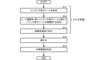
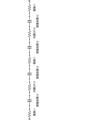
- Fig. 4 is a flow chart showing an example of a schematic flow of the method for manufacturing the solid electrolytic capacitor according to the first embodiment.
- a capacitor element sheet is formed (FIG. 4: S11).
- a plurality of first capacitor elements 10A that form different solid electrolytic capacitors 1 are formed in an array on the first capacitor element sheet.
- a plurality of second capacitor elements 10B that form different solid electrolytic capacitors 1 are formed in an array on the second capacitor element sheet.
- the first capacitor element sheet and the second capacitor element sheet are laminated to form a sheet laminate (FIG. 4: S12).
- the sheet laminate is a structure in which a plurality of capacitor element laminates 100 are arranged in a plane.
- the sheet laminate is sealed with insulating resin 50 (Fig. 4: S13). Details will be described later, but at this time, through holes that penetrate from the top surface to the bottom surface of the sheet laminate are provided in the sheet laminate, and resin sealing is performed by compression molding.
- the solid electrolytic capacitor 1 is in a multi-state (a state in which multiple solid electrolytic capacitors 1 are arranged) before being separated into individual pieces.
- the sheet laminate sealed with insulating resin 50 is cut and separated into individual pieces (FIG. 4: S14). Specifically, the cutting is performed along the cutting lines formed at any position. As a result, a plurality of solid electrolytic capacitors 1 (referred to as the body of solid electrolytic capacitor 1) without external electrodes are formed. After this, the body of solid electrolytic capacitor 1 is secondary sealed with insulating resin 50. More specifically, the side surfaces of the body of solid electrolytic capacitor 1 (surfaces cut along the cutting lines formed at any position (upper surface, lower surface, and side surfaces other than the end surfaces where the electrodes 11 of the first capacitor element 10A and the electrodes 11 of the second capacitor element 10B are exposed)) are covered with secondary sealing of insulating resin 50. As a result, the electrodes 11 of the first capacitor element 10A and the electrodes 11 of the second capacitor element 10B that are unnecessarily exposed during singulation are covered with insulating resin 50.
- FIG. 5 is a flow chart showing an example of a forming process of a capacitor element sheet.
- Fig. 6(A) is an external perspective view showing the shape of the electrodes of the capacitor element before singulation
- Fig. 6(B) is an external perspective view showing the shape of the capacitor element before singulation.
- Fig. 7 is an external view of the capacitor element in a multi-state. In the following forming process, the forming process of the first capacitor element 10A and the second capacitor element 10B are the same. Here, the first capacitor element 10A will be described as an example.
- the electrode 11 of the first capacitor element 10A is subjected to a chemical conversion treatment to form the dielectric layer 12 (FIG. 5: S111). At this time, a large number of holes are formed on the surface of the electrode 11 by etching, and the area near the surface of the electrode 11 is porous.
- the dielectric layer 12 covers the surface of the electrode 11, including the inner surfaces of the holes.
- through holes are formed in the electrode 11 (FIG. 5: S112). More specifically, as shown in FIG. 6(A), a plurality of cylindrical through holes 19C and groove-shaped through holes 19L are formed in the electrode 11.
- the plurality of cylindrical through holes 19C and groove-shaped through holes 19L are arranged alternately along the direction in which the portions that will become the plurality of electrodes 11 are arranged.
- the plurality of cylindrical through holes 19C are formed at a position that realizes the first end EA1 of the electrode 11, and the groove-shaped through holes 19L are formed at a position that straddles the portions that will become the adjacent electrodes 11 and at a position that realizes the second end EA2 of the adjacent electrodes 11.
- a CP layer (solid electrolyte layer) 13 is formed on the surface of the dielectric layer 12 (FIG. 5: S113). More specifically, as shown in FIG. 6(B), a first dam 14 having a frame-shaped opening is formed. Then, a CP layer 13 (a laminated structure of an inner layer CP 131 and an outer layer CP 132) is formed within the opening of the first dam 14.
- this structure is made in a multi-state in which multiple capacitor elements 10 (structures consisting of electrodes 11, dielectric layers 12, CP layers 13, and first dams 14) are arranged two-dimensionally. As described above, cutting is performed along the cutting lines to form solid electrolytic capacitors 1. This forms multiple solid electrolytic capacitors 1 (referred to as solid electrolytic capacitor 1 bodies) without external electrodes formed.
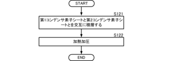
- Fig. 8 is a flow chart showing an example of a process for forming a sheet laminate.
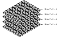
- Fig. 9 is an exploded perspective view showing a state in which a first capacitor element sheet and a second capacitor element sheet are laminated.
- Fig. 10 is an exploded perspective view showing a state in which a pair of a first capacitor element 10A and a second capacitor element 10B are laminated.
- the first capacitor element sheets and the second capacitor element sheets are alternately stacked (FIG. 8: S121). At this time, the first capacitor element sheets and the second capacitor element sheets are stacked so that their orientations are staggered. This makes it possible to realize a structure in which the first end E1 of the first capacitor element 10A and the second end E2 of the second capacitor element 10B protrude, as shown in FIG. 1, for example.
- the first capacitor element 10A and the second capacitor element 10B are alternately stacked.
- the through hole 19C of the first capacitor element 10A overlaps with the through hole 19L of the second capacitor element 10B when viewed in the stacking direction (Z-axis direction in Figure 10).
- the through hole 19L of the first capacitor element 10A overlaps with the through hole 19C of the second capacitor element 10B when viewed in the stacking direction (Z-axis direction in Figure 10).
- the through hole 19C of the first capacitor element 10A overlaps with the through hole 19L of the second capacitor element 10B when viewed in the stacking direction (the Z-axis direction in FIG. 10), and the through hole 19L of the first capacitor element 10A overlaps with the through hole 19C of the second capacitor element 10B.
- These through holes are formed in a number corresponding to the number of capacitor elements arranged in the sheet laminate.
- the sheet laminate is formed with a number of through holes that penetrate from the top surface to the bottom surface of the sheet laminate.
- the sheet laminate is heated and pressurized (FIG. 8: S122). This bonds the first capacitor element sheet and the second capacitor element sheet together to form a sheet laminate. Note that the first capacitor element sheet and the second capacitor element sheet are bonded together by the outer layer CP132 as described above.
- Fig. 11 is a side cross-sectional view showing the configuration of the solid electrolytic capacitor according to the second embodiment.
- Fig. 12 is a side cross-sectional view showing an outline of a structure in which capacitor elements according to the second embodiment are stacked.
- Fig. 13(A) is an external perspective view showing the shape of the electrodes of a third capacitor element before singulation, and
- Fig. 13(B) is an external perspective view showing the shape of the third capacitor element before singulation.
- the solid electrolytic capacitor 1A according to the second embodiment differs from the solid electrolytic capacitor 1 according to the first embodiment in that it includes a third capacitor element 10C.
- the other configuration of the solid electrolytic capacitor 1A is the same as that of the solid electrolytic capacitor 1, and a description of similar parts will be omitted.
- the number (number) of the flat film-shaped first capacitor element 10A, second capacitor element 10B, and third capacitor element 10C is one each, but this is not limited to this.
- the capacitor element laminate 100A comprises a flat film-shaped first capacitor element 10A, a second capacitor element 10B, and a third capacitor element 10C.
- the external electrode 61 corresponds to the "first pole” (positive pole) in the present invention
- the external electrode 62 corresponds to the "second pole” (negative pole) in the present invention.
- the first capacitor element 10A and the second capacitor element 10B have a flat film-shaped electrode 11, a dielectric layer 12, and a CP layer (solid electrolyte layer) 13.
- the third capacitor element 10C has a flat film-shaped electrode 11C, a dielectric layer 12, and a CP layer (solid electrolyte layer) 13.
- the dielectric layer 12 and the CP layer 13 have the same configuration as the first capacitor element 10A and the second capacitor element 10B.
- the first capacitor element 10A and the third capacitor element 10C are stacked so that their flat film surfaces are parallel and overlap when viewed from above.
- the third capacitor element 10C and the second capacitor element 10B are stacked so that their flat film surfaces are parallel and overlap when viewed from above.
- the first capacitor element 10A, the third capacitor element 10C, and the second capacitor element 10B are stacked alternately so that their respective flat film surfaces are parallel and overlap when viewed from above.
- An outer layer CP132 exists between the first capacitor element 10A and the third capacitor element 10C.
- the first capacitor element 10A and the third capacitor element 10C are bonded together using this outer layer CP132.
- an outer layer CP132 exists between the third capacitor element 10C and the second capacitor element 10B.
- the third capacitor element 10C and the second capacitor element 10B are bonded together using this outer layer CP132.
- the thickness of the solid electrolytic capacitor 1A can be reduced by the amount of the omitted outer layer CP132.
- the first end EA1 of the first capacitor element 10A, the second end EB2 of the second capacitor element 10B, and the first end EC1 of the third capacitor are arranged on the first end side of the capacitor element stack 100.
- the first end EA1 of the first capacitor element 10A protrudes outward beyond the second end EB2 of the second capacitor element 10B and the first end EC1 of the third capacitor.
- the first end EB1 of the second capacitor element 10B, the second end EA2 of the first capacitor element 10A, and the second end EC2 of the third capacitor are arranged on the second end side of the capacitor element stack 100.
- the first end EB1 of the second capacitor element 10B and the second end EC2 of the third capacitor protrude outward beyond the second end EA2 of the first capacitor element 10A.
- the first end EC1 of the third capacitor element 10C is not connected to the external electrode 61. Also, the second end EC2 is not connected to the external electrode 62.
- a through hole is formed in the electrode 11C. More specifically, a groove-shaped through hole 19L is formed at both ends of the electrode 11C. The groove-shaped through hole 19L is formed at a position that realizes the first end EC1 and the second end EC2 of the third capacitor element 10C.
- the capacitor element laminate 100A is sealed with insulating resin 50. More specifically, the insulating resin 50 covers the capacitor element laminate 100A except for the first end EA1 of the first capacitor element 10A and the first end EB1 of the second capacitor element 10B.
- the external electrode 61 covers the first end of the insulating resin 50 (the first end EA1 of the first capacitor element 10A).
- the external electrode 61 is connected to the first ends EA1 of the electrodes 11 of the multiple first capacitor elements 10A.
- the external electrode 62 covers the second end of the insulating resin 50 (the first end EB1 of the second capacitor element 10B).
- the external electrode 62 is connected to the first ends EB1 of the electrodes 11 of the multiple second capacitor elements 10B.
- the first capacitor element 10A, the third capacitor element 10C, and the second capacitor element 10B are connected in series.
- the withstand voltage across both ends of solid electrolytic capacitor 1A is the sum of the withstand voltage of first capacitor element 10A, the withstand voltage of second capacitor element 10B, and the withstand voltage of third capacitor element 10C.
- the present invention can realize a solid electrolytic capacitor with high voltage resistance compared to conventional solid electrolytic capacitors formed by stacking cathode and anode electrodes.
- Fig. 15 is a side cross-sectional view showing the configuration of the solid electrolytic capacitor according to the third embodiment.
- Fig. 16 is a side cross-sectional view showing an outline of a structure in which capacitor elements according to the third embodiment are stacked.
- the solid electrolytic capacitor 1B according to the third embodiment differs from the solid electrolytic capacitor 1A according to the second embodiment in that it includes a plurality of third capacitor elements 10C.
- the other configuration of the solid electrolytic capacitor 1B is the same as that of the solid electrolytic capacitor 1A, and a description of similar parts will be omitted.
- the capacitor element laminate 100A comprises a plurality of flat film-shaped first capacitor elements 10A, second capacitor elements 10B, and a plurality of third capacitor elements 10C.
- the external electrode 61 corresponds to the "first external electrode” (positive electrode) in the present invention
- the external electrode 62 corresponds to the "second external electrode” (negative electrode) in the present invention.
- the first capacitor element 10A and the third capacitor element 10C are stacked so that their flat film surfaces are parallel and overlap when viewed from above.
- the third capacitor element 10C and the third capacitor element 10C are stacked so that their flat film surfaces are parallel and overlap when viewed from above.
- the third capacitor element 10C and the second capacitor element 10B are stacked so that their flat film surfaces are parallel and overlap when viewed from above.
- the first capacitor element 10A and the multiple third capacitor elements 10C and the second capacitor element 10B are stacked alternately so that their respective flat film surfaces are parallel and overlap when viewed from above.
- An outer layer CP132 exists between the first capacitor element 10A and the third capacitor element 10C.
- the first capacitor element 10A and the third capacitor element 10C are bonded together using this outer layer CP132.
- an outer layer CP132 is present between the third capacitor element 10C and the third capacitor element 10C.
- this outer layer CP132 By using this outer layer CP132, the third capacitor element 10C and the third capacitor element 10C are bonded together.
- an outer layer CP132 exists between the third capacitor element 10C and the second capacitor element 10B.
- this outer layer CP132 the third capacitor element 10C and the second capacitor element 10B are bonded together.
- the thickness of the solid electrolytic capacitor 1B can be made thinner by the amount of the omitted outer layer CP132.
- the first end EA1 of the first capacitor element 10A, the second end EB2 of the second capacitor element 10B, and the first end EC1 of the third capacitor are arranged on the first end side of the capacitor element stack 100.
- the first end EA1 of the first capacitor element 10A protrudes outward beyond the second end EB2 of the second capacitor element 10B and the first end EC1 of the third capacitor.
- the first end EB1 of the second capacitor element 10B, the second end EA2 of the first capacitor element 10A, and the second end EC2 of the third capacitor are arranged on the second end side of the capacitor element stack 100.
- the first end EB1 of the second capacitor element 10B and the second end EC2 of the third capacitor protrude outward beyond the second end EA2 of the first capacitor element 10A.
- the capacitor element laminate 100B is sealed with insulating resin 50. More specifically, the insulating resin 50 covers the capacitor element laminate 100B except for the first end EA1 of the first capacitor element 10A and the first end EB1 of the second capacitor element 10B.
- the external electrode 61 covers the first end of the insulating resin 50.
- the external electrode 61 is connected to the first ends EA1 of the electrodes 11 of the multiple first capacitor elements 10A.
- the external electrode 62 covers the second end of the insulating resin 50.
- the external electrode 62 is connected to the first ends EB1 of the electrodes 11 of the multiple second capacitor elements 10B.
- the withstand voltage across the solid electrolytic capacitor 1B is the sum of the withstand voltage of the first capacitor element 10A, the withstand voltage of the second capacitor element 10B, and the withstand voltage of the multiple third capacitor elements 10C.
- the present invention can realize a solid electrolytic capacitor with high voltage resistance compared to conventional solid electrolytic capacitors formed by stacking cathode and anode electrodes.
- Fig. 17 is a side cross-sectional view showing an outline of a structure in which capacitor elements according to the fourth embodiment are stacked.
- the solid electrolytic capacitor 1C according to the fourth embodiment differs from the solid electrolytic capacitor 1A according to the second embodiment in that it includes a plurality of first capacitor elements 10A, a plurality of second capacitor elements 10B, and a plurality of third capacitor elements 10C.
- the other configuration of the solid electrolytic capacitor 1C is the same as that of the solid electrolytic capacitor 1A, and a description of similar parts will be omitted.
- the capacitor element laminate 100C is laminated in the following order: first capacitor element 10A, third capacitor element 10C, second capacitor element 10B, third capacitor element 10C, first capacitor element 10A, third capacitor element 10C, and second capacitor element 10B.
- the withstand voltage across both ends of solid electrolytic capacitor 1C is the sum of the withstand voltage of first capacitor element 10A, the withstand voltage of third capacitor element 10C, the withstand voltage of second capacitor element 10B, the withstand voltage of third capacitor element 10C, the withstand voltage of first capacitor element 10A, the withstand voltage of third capacitor element 10C, and the withstand voltage of second capacitor element 10B.
- the present invention can realize a solid electrolytic capacitor with high voltage resistance compared to conventional solid electrolytic capacitors formed by stacking cathode and anode electrodes.
- the number of first capacitor elements 10A and the number of second capacitor elements 10B are the same, but they can also be different.
- the number of first capacitor elements 10A, the number of second capacitor elements 10B, and the number of third capacitor elements 10C may be determined by appropriate combination to obtain the desired withstand voltage (high withstand voltage) and capacitance (high capacity). If the number of first capacitor elements 10A and the number of second capacitor elements 10B are the same, a non-polar (bipolar) solid electrolytic capacitor can be realized.
- the capacitor element 10 (first capacitor element, second capacitor element, third capacitor element) is realized, for example, with the following materials and thicknesses.
- the electrode 11 is made of, for example, a single metal such as aluminum, tantalum, niobium, titanium, zirconium, magnesium, copper, or an alloy containing these metals.
- the electrode 11 (electrode 11C) is preferably made of aluminum or an aluminum alloy.
- the electrode 11 (electrode 11C) may be any valve action metal that exhibits so-called valve action.
- the electrode 11 is preferably flat, and the thickness of the core (the center part not reached by the pores of the porous body) of the electrode 11 (electrode 11C) is preferably 5 ⁇ m or more and 100 ⁇ m or less.
- the thickness (thickness of one side) of the porous part is preferably 5 ⁇ m or more and 200 ⁇ m or less.
- the dielectric layer 12 is preferably made of an oxide film of the electrode 11 (electrode 11C).
- the dielectric layer 12 is formed by oxidizing it in an aqueous solution containing boric acid, phosphoric acid, adipic acid, or their sodium salts, ammonium salts, etc.
- the thickness of the dielectric layer 12 is preferably 1 nm or more and 100 nm or less.
- the inner layer CP131 may be a layer of PEDOT:PSS, which is realized by, for example, a conductive polymer having a skeleton of pyrroles, thiophenes, anilines, etc., or a conductive polymer having a skeleton of thiophenes such as PEDOT [poly(3,4-ethylenedioxythiophene)], which is a conductive polymer having a skeleton of thiophenes, and is composited with polystyrene sulfonic acid (PSS) as a dopant.
- PEDOT poly(3,4-ethylenedioxythiophene)
- the inner layer CP131 is formed, for example, by a method of forming a polymer film of poly(3,4-ethylenedioxythiophene) or the like on the surface of the dielectric layer 12 using a treatment liquid containing a monomer such as 3,4-ethylenedioxythiophene, or a method of applying a dispersion of a polymer such as poly(3,4-ethylenedioxythiophene) to the surface of the dielectric part and drying it.
- the thickness of the outer layer CP132 is preferably 2 ⁇ m or more and 20 ⁇ m or less.
- the material of the outer layer CP132 is the same as the material of the inner layer CP131.
- the insulating resin 50 may contain a filler.
- the resin are preferably epoxy resin, phenol resin, polyimide resin, silicone resin, polyamide resin, liquid crystal polymer, etc.
- the filler are preferably insulating oxide particles such as silica particles, alumina particles, titania particles, zirconia particles, etc.
- the maximum diameter of the filler is preferably, for example, 10 ⁇ m or more and 50 ⁇ m or less.
- a material containing silica particles in solid epoxy resin and phenol resin is more preferable.
- the capacitor further includes a plurality of flat-film-shaped third capacitor elements each having a dielectric layer and a solid electrolyte layer formed in that order on a surface of a flat-film-shaped electrode foil,
- the first external electrode is formed on a first end surface of the sheet laminate
Abstract
固体電解コンデンサは、それぞれの平膜状の電極箔の表面に誘電体層が形成され、誘電体層の表面に固体電解質層が形成された第1コンデンサ素子と第2コンデンサ素子を積層して形成されたシート積層体と、シート積層体を封止する絶縁性樹脂と、を備える。シート積層体の第1端から第1コンデンサ素子の電極箔を引き出すことで第1極を形成し、シート積層体の第1端に対向する第2端から第2コンデンサ素子の電極箔を引き出すことで第2極を形成する。
Description
本発明は、複数のコンデンサ素子積層した積層体を備える固体電解コンデンサに関する。
特許文献1には、固体電解コンデンサの製造方法および固体電解コンデンサが記載されている。特許文献1に記載の固体電解コンデンサは、複数の平膜状のコンデンサ素子と複数の金属箔(陰極)とを備える。平膜状のコンデンサ素子は、箔状の弁作用金属基体(陽極)、弁作用金属基体の多孔質部および表面に形成された誘電体層、誘電体層の表面に形成された固体電解質層を備える。
より具体的には、次の構成を備える。特許文献1のコンデンサ素子における多孔質部に絶縁性樹脂(マスク部材)が含侵されている。さらに、この絶縁性樹脂には絶縁性接着剤が枠状に形成されている。そして、絶縁性接着剤の枠内には、固体電解質層が形成されている。平膜状のコンデンサ素子と金属箔とは交互に積層されている。これにより、素子積層体が形成される。
しかしながら、特許文献1に示すような固体電解コンデンサを用いた場合、コンデンサ素子は並列接続される。すなわち、当該固体電解コンデンサの耐電圧を上昇させるためには、コンデンサ素子の積層数を増やす必要がある。すなわち、固体電解コンデンサのサイズは大きくなってしまう。
したがって、本発明の目的は、高耐圧、小型化を実現し、かつ製造が容易な固体電解コンデンサを提供することにある。
この発明の固体電解コンデンサは、それぞれの平膜状の電極箔の表面に誘電体層が形成され、誘電体層の表面に固体電解質層が形成された第1コンデンサ素子と第2コンデンサ素子を積層して形成されたシート積層体と、シート積層体を封止する絶縁性樹脂と、を備える。シート積層体の第1端面から第1コンデンサ素子の電極箔を引き出すことで第1極を形成し、シート積層体の第1端面に対向する第2端面から第2コンデンサ素子の電極箔を引き出すことで第2極を形成する。
この構成を備えることで、無極性の固体電解コンデンサを容易に形成することができる。また、各コンデンサ素子を直列接続するため、高耐圧を実現できる。
この発明によれば、高耐圧、小型化を実現し、かつ製造が容易な固体電解コンデンサを提供できる。
[第1の実施形態]
本発明の第1の実施形態に係る固体電解コンデンサ、およびこの固体電解コンデンサの製造方法について、図を参照して説明する。
本発明の第1の実施形態に係る固体電解コンデンサ、およびこの固体電解コンデンサの製造方法について、図を参照して説明する。
(固体電解コンデンサ1の概略的な構成の説明)
まず、本発明の実施形態に係る固体電解コンデンサの構造について説明する。図1は、第1の実施形態に係る固体電解コンデンサの構成を示す側面断面図である。なお、図1では、図を見やすくするため、絶縁性樹脂および外部電極のみをハッチングしている。図2(A)は、個片化前のコンデンサ素子の構成を示す側面断面図であり、図2(B)はコンデンサ素子を積層した構造の概要を示す側面断面図である。
まず、本発明の実施形態に係る固体電解コンデンサの構造について説明する。図1は、第1の実施形態に係る固体電解コンデンサの構成を示す側面断面図である。なお、図1では、図を見やすくするため、絶縁性樹脂および外部電極のみをハッチングしている。図2(A)は、個片化前のコンデンサ素子の構成を示す側面断面図であり、図2(B)はコンデンサ素子を積層した構造の概要を示す側面断面図である。
図1、図2(A)、図2(B)に示すように、固体電解コンデンサ1は、コンデンサ素子積層体100、絶縁性樹脂50、外部電極61、および外部電極62を備える。コンデンサ素子積層体100は、複数の平膜状の第1コンデンサ素子10Aおよび複数の第2コンデンサ素子10Bを備える。なお、図1では、平膜状の第1コンデンサ素子10Aおよび第2コンデンサ素子10Bの個数(枚数)は、それぞれに2であるが、これに限るものではない。なお、外部電極61が本発明における「第1外部電極」に対応し、外部電極62が本発明における「第2外部電極」に対応する。
図2(A)に示すように、第1コンデンサ素子10A、第2コンデンサ素子10Bは、平膜状の電極11、誘電体層12、およびCP層(固体電解質層)13を備える。電極11が本発明の「電極箔」に対応する。
図2(A)、図2(B)では詳細な構造の図示は割愛されているが、電極11は、多数の孔を備える。言い換えれば、電極11は、ポーラス状態(多孔質体)である。電極11の一方側の多孔質部分と芯金部分と他方側の多孔質部分の厚みの比は、1:1:1程度となっている。誘電体層12は、電極11の外面を覆う。図2(A)、図2(B)では電極11の詳細な構造の図示が割愛されているため、誘電体層12は模式的に電極11の巨視的な表面を覆っているように図示されている。実際には、誘電体層12は、電極11の巨視的な表面のみならず、電極11の多数の孔の表面も覆っている。
CP層13は、誘電体層12の表面を覆う。CP層13は、枠状の第1ダム14の内部に形成されている。第1ダム14は、絶縁性を有する。第1ダム14によって、CP層13の形成領域が規制される。なお、第1の実施形態では、後述する製造方法で説明されるように、第1ダム14が枠状に形成された後、第1ダム14の内部にCP層13が形成される。しかしながら、例えば最初から個片化された状態でコンデンサ素子10を作成する場合など、コンデンサ素子10の製造方法によっては、第1ダム14は、枠状に形成されていなくてもよい。すなわち、第1ダム14は、1辺に形成されていてもよいし、角を有する2辺に形成されていてもよい。さらには、平面視において対向する2辺に形成されている構造であってもよい。なお、CP層が誘電体層12の表面のみに形成できる場合には、第1ダム14は省略されていてもよい。
CP層13は、内層CP(内層固体電解質層)131と外層CP(外層固体電解質層)132との積層構造である。内層CP131は、誘電体層12の表面に形成され、外層CP132は、内層CP131の表面に形成される。
複数の第1コンデンサ素子10Aと複数の第2コンデンサ素子10Bとは、それぞれの平膜面が平行になるように、且つ、平面視して重なり合うように交互に積層されている。
第1コンデンサ素子10Aと第2コンデンサ素子10Bとの間には、それぞれの外層CP(外層固体電解質層)132が配置されている。この外層CP132を用いることで、第1コンデンサ素子10Aと第2コンデンサ素子10Bとは接着する。
また、第1コンデンサ素子10Aと第2コンデンサ素子10Bとの間には、外層CP132に当接するようにカーボン層が形成されていてもよい。カーボン層が形成されていることにより、第1コンデンサ素子10Aと第2コンデンサ素子10Bとの密着強度を向上させることができ、低抵抗が実現される。なお、カーボン層が形成される場合は、カーボン層の形成領域を規制するための第2ダム(図示を省略)が存在することが好ましい。
なお、第1コンデンサ素子10Aと第2コンデンサ素子10Bのそれぞれが外層CP132を有する例を示したが、第1コンデンサ素子10Aと第2コンデンサ素子10Bとが当接する面においては、どちらか一方の外層CP132を省略することも可能である。この場合、固体電解コンデンサ1の厚みは省略された外層CP132の分だけ薄くすることが可能である。
このような積層状態において、複数の第1コンデンサ素子10Aの第1端EA1は、側面視して略同じ位置となる。同様に、複数の第1コンデンサ素子10Aの第2端EA2は、側面視して略同じ位置となる。また、複数の第2コンデンサ素子10Bの第1端EB1は、側面視して略同じ位置となる。同様に、複数の第2コンデンサ素子10Bの第2端EB2は、側面視して略同じ位置となる。
複数の第1コンデンサ素子10Aの第1端EA1と複数の第2コンデンサ素子10Bの第2端EB2とは、コンデンサ素子積層体100の第1端側に配置される。複数の第1コンデンサ素子10Aの第1端EA1は、複数の第2コンデンサ素子10Bの第2端EB2よりも外方に突出している。第1コンデンサ素子10Aの第1端EA1が本発明の「第1極」に対応する。この第1端EA1は、コンデンサ素子積層体100の第1端面の一部である。
複数の第2コンデンサ素子10Bの第1端EB1と複数の第1コンデンサ素子10Aの第2端EA2とは、コンデンサ素子積層体100の第2端側に配置される。複数の第2コンデンサ素子10Bの第1端EB1は、複数の第1コンデンサ素子10Aの第2端EA2よりも外方に突出している。第2コンデンサ素子10Bの第1端EB1が本発明の「第2極」に対応する。この第1端EB1は、コンデンサ素子積層体100の第2端面の一部である。
このような構造によって、コンデンサ素子積層体100は実現される。
コンデンサ素子積層体100は、絶縁性樹脂50によって封止される。より具体的には、絶縁性樹脂50は、複数の第1コンデンサ素子10Aの第1端EA1および複数の第2コンデンサ素子10Bの第1端EB1を除き、コンデンサ素子積層体100を覆う。
外部電極61は、絶縁性樹脂50の第1端(第1コンデンサ素子10Aの第1端EA1)を覆う。外部電極61は、複数の第1コンデンサ素子10Aの電極11の第1端EA1に接続する。
外部電極62は、絶縁性樹脂50の第2端(第2コンデンサ素子10Bの第1端EB1)を覆う。外部電極62は、複数の第2コンデンサ素子10Bの電極11の第1端EB1に接続する。
以上の構成によって、第1の実施形態における無極性(バイポーラ)の固体電解コンデンサ1は実現される。言い換えれば、固体電解コンデンサ1は、外部電極61から外部電極62へ向かう構造と外部電極62から外部電極61に向かう構造とが同じ対称形である。なお、第1コンデンサ素子10Aと第2コンデンサ素子10Bを、異なる記号を付して説明したが、第1の実施形態においては、第1コンデンサ素子10Aと第2コンデンサ素子10Bとは同一の構成である。ただし、第1コンデンサ素子10Aと第2コンデンサ素子10Bとは異なる構成であってもよい。
ここで、第1コンデンサ素子10Aと第2コンデンサ素子10Bとが同一の構成である場合と異なる構成である場合とを比較する。第1コンデンサ素子10Aと第2コンデンサ素子10Bとが同一の構成であると、容量効率がよく、固体電解コンデンサ1に対する電圧のバランスを均等に設計することができる。
(固体電解コンデンサ1の回路構成)
次に、図3を用いて、固体電解コンデンサ1の回路構成について説明する。なお、図3は、一対の第1コンデンサ素子10Aと第2コンデンサ素子10Bによる回路を示す。固体電解コンデンサ1の等価回路図に示すように、第1コンデンサ素子10A、第2コンデンサ素子10B、第1コンデンサ素子10A、第2コンデンサ素子10Bは直列接続されている。
次に、図3を用いて、固体電解コンデンサ1の回路構成について説明する。なお、図3は、一対の第1コンデンサ素子10Aと第2コンデンサ素子10Bによる回路を示す。固体電解コンデンサ1の等価回路図に示すように、第1コンデンサ素子10A、第2コンデンサ素子10B、第1コンデンサ素子10A、第2コンデンサ素子10Bは直列接続されている。
すなわち、固体電解コンデンサ1の両端の耐電圧は、第1コンデンサ素子10Aの耐電圧、第2コンデンサ素子10Bの耐電圧、第1コンデンサ素子10Aの耐電圧、第2コンデンサ素子10Bの耐電圧の和となる。
このことから、陰極電極および陽極電極を積層することによって形成される従来構成の固体電解コンデンサと比較すると、本発明は高耐圧の固体電解コンデンサを容易に実現できる。特に、第1コンデンサ素子10Aと第2コンデンサ素子10Bとがそれぞれ二組以上ある場合、並列接続されるコンデンサが存在するので、より確実な高耐圧化を実現できる。
(固体電解コンデンサ1の製造方法)
上述の構成からなる固体電解コンデンサ1は、例えば、次のように製造される。図4は、第1の実施形態に係る固体電解コンデンサの製造方法の概略フローの一例を示すフローチャートである。
上述の構成からなる固体電解コンデンサ1は、例えば、次のように製造される。図4は、第1の実施形態に係る固体電解コンデンサの製造方法の概略フローの一例を示すフローチャートである。
コンデンサ素子シートを形成する(図4:S11)。第1コンデンサ素子シートには、それぞれの異なる固体電解コンデンサ1を形成する複数の第1コンデンサ素子10Aが配列された状態で形成されている。同様に、第2コンデンサ素子シートには、それぞれの異なる固体電解コンデンサ1を形成する複数の第2コンデンサ素子10Bが配列された状態で形成されている。
次に、第1コンデンサ素子シートと第2コンデンサ素子シートを積層し、シート積層体を形成する(図4:S12)。これにより、複数のコンデンサ素子積層体100が平面的に配列された構造体が形成される。言い換えれば、シート積層体とは、複数のコンデンサ素子積層体100が平面的に配列されたものである。
次に、シート積層体を絶縁性樹脂50で封止する(図4:S13)。詳細は後述するが、この際に、シート積層体の上面から下面までを貫通する貫通穴をシート積層体に備え、コンプレッションモールドによって樹脂封止を行う。
この絶縁性樹脂50での封止までは、固体電解コンデンサ1が個片化される前のマルチ状態(複数の固体電解コンデンサ1となるものが配列された状態)で行われる。
次に、絶縁性樹脂50で封止されたシート積層体を切断し、個片化する(図4:S14)。具体的には、任意の位置に形成された切断線に沿って切断を行う。これにより、外部電極が形成されていない状態の複数の固体電解コンデンサ1(固体電解コンデンサ1の素体と称する)が形成される。この後、固体電解コンデンサ1の素体に絶縁性樹脂50の2次封止を行う。より具体的には、固体電解コンデンサ1の素体の側面(任意の位置に形成された切断線で切断した面(上面、下面、第1コンデンサ素子10Aの電極11および第2コンデンサ素子10Bの電極11が露出する端面とは異なる側面))を、絶縁性樹脂50の2次封止によって覆う。これにより、個片化時に不要に露出する第1コンデンサ素子10Aの電極11および第2コンデンサ素子10Bの電極11を絶縁性樹脂50で覆う。
次に、固体電解コンデンサ1の素体の端面に外部電極61および外部電極62を形成する(図4:S15)。
次に、各工程をより具体的に説明する。
(コンデンサ素子シートの形成工程)
図5は、コンデンサ素子シートの形成工程の一例を示すフローチャートである。図6(A)は、個片化前のコンデンサ素子の電極の形状を示す外観斜視図であり、図6(B)は、個片化前のコンデンサ素子の形状を示す外観斜視図である。図7は、コンデンサ素子のマルチ状態での外観図である。以下の形成工程において、第1コンデンサ素子10Aと第2コンデンサ素子10Bの形成工程は同様である。ここでは、第1コンデンサ素子10Aを例に説明する。
図5は、コンデンサ素子シートの形成工程の一例を示すフローチャートである。図6(A)は、個片化前のコンデンサ素子の電極の形状を示す外観斜視図であり、図6(B)は、個片化前のコンデンサ素子の形状を示す外観斜視図である。図7は、コンデンサ素子のマルチ状態での外観図である。以下の形成工程において、第1コンデンサ素子10Aと第2コンデンサ素子10Bの形成工程は同様である。ここでは、第1コンデンサ素子10Aを例に説明する。
第1コンデンサ素子10Aの電極11に化成処理を行って、誘電体層12を形成する(図5:S111)。この際、電極11の表面には、エッチングによって多数の孔が形成されており、電極11の表面付近は多孔質体となっている。誘電体層12は、孔の内面も含めた電極11の表面を覆っている。
次に、電極11に貫通穴を形成する(図5:S112)。より具体的には、図6(A)に示すように、電極11には、複数の円筒形の貫通穴19Cと、溝状の貫通穴19Lとが形成される。複数の円筒形の貫通穴19Cと、溝状の貫通穴19Lとは、複数の電極11となる部分の並ぶ方向に沿って、交互に配列されている。複数の円筒形の貫通穴19Cは、電極11の第1端EA1を実現する位置に形成され、溝状の貫通穴19Lは、隣り合う電極11となる部分を跨ぐ位置、および、隣り合う電極11の第2端EA2を実現する位置に形成される。
次に、誘電体層12の表面にCP層(固体電解質層)13を形成する(図5:S113)。より具体的には、図6(B)に示すように、枠状の開口を有する第1ダム14を形成する。そして、第1ダム14の開口内に、CP層13(内層CP131と外層CP132との積層構造)を形成する。
この構造は、図7に示すように、複数のコンデンサ素子10(電極11、誘電体層12、CP層13、および第1ダム14からなる構造体)が二次元で配列されたマルチ状態で行われる。上述のとおり、固体電解コンデンサ1を形成するための切断線に沿って切断を行う。これにより、外部電極が形成されていない状態の複数の固体電解コンデンサ1(固体電解コンデンサ1の素体と称する)が形成される。
(シート積層体の形成工程)
図8は、シート積層体の形成工程の一例を示すフローチャートである。図9は、第1コンデンサ素子シートと第2コンデンサ素子シートとを積層する状態を示す分解斜視図である。図10は、1組の第1コンデンサ素子10Aと第2コンデンサ素子10Bの積層する状態を示す分解斜視図である。
図8は、シート積層体の形成工程の一例を示すフローチャートである。図9は、第1コンデンサ素子シートと第2コンデンサ素子シートとを積層する状態を示す分解斜視図である。図10は、1組の第1コンデンサ素子10Aと第2コンデンサ素子10Bの積層する状態を示す分解斜視図である。
図9に示すように、第1コンデンサ素子シートと第2コンデンサ素子シートとを交互に積層する(図8:S121)。この際、第1コンデンサ素子シートと第2コンデンサ素子シートとは、向きが互い違いになるように積層される。このことによって、例えば図1に示すように、第1コンデンサ素子10Aの第1端E1、第2コンデンサ素子10Bの第2端E2が突出する構造を実現できる。
より具体的には、図9、図10に示すように、第1コンデンサ素子10Aと第2コンデンサ素子10Bは交互に積層される。この際、第1コンデンサ素子10Aの貫通穴19Cは、積層方向(図10におけるZ軸方向)に視て、第2コンデンサ素子10Bの貫通穴19Lと重なる。同様に、第1コンデンサ素子10Aの貫通穴19Lは、積層方向(図10におけるZ軸方向)に視て、第2コンデンサ素子10Bの貫通穴19Cと重なる。
第1コンデンサ素子10Aと第2コンデンサ素子10Bを複数積層した場合においても同様に、第1コンデンサ素子10Aの貫通穴19Cは、積層方向(図10におけるZ軸方向)に視て、第2コンデンサ素子10Bの貫通穴19Lが重なり、第1コンデンサ素子10Aの貫通穴19Lは、第2コンデンサ素子10Bの貫通穴19Cと重なるように積層される。
そして、これらの貫通穴は、シート積層体に配列されたコンデンサ素子の個数に応じて複数形成される。したがって、シート積層体には、シート積層体の上面から下面まで貫通する貫通穴が複数形成される。
次に、シート積層体を加熱加圧する(図8:S122)。これにより、第1コンデンサ素子シートと第2コンデンサ素子シートとが接着され、シート積層体が形成される。なお、第1コンデンサ素子シートと第2コンデンサ素子シートとは、上述したとおり外層CP132によって接着される。
[第2の実施形態]
次に、第2の実施形態に係る固体電解コンデンサについて、図を参照して説明する。図11は、第2の実施形態に係る固体電解コンデンサの構成を示す側面断面図である。図12は、第2の実施形態に係るコンデンサ素子を積層した構造の概要を示す側面断面図である。図13(A)は、個片化前の第3コンデンサ素子の電極の形状を示す外観斜視図であり、図13(B)は、個片化前の第3コンデンサ素子の形状を示す外観斜視図である。
次に、第2の実施形態に係る固体電解コンデンサについて、図を参照して説明する。図11は、第2の実施形態に係る固体電解コンデンサの構成を示す側面断面図である。図12は、第2の実施形態に係るコンデンサ素子を積層した構造の概要を示す側面断面図である。図13(A)は、個片化前の第3コンデンサ素子の電極の形状を示す外観斜視図であり、図13(B)は、個片化前の第3コンデンサ素子の形状を示す外観斜視図である。
図11に示すように、第2の実施形態に係る固体電解コンデンサ1Aは、第1の実施形態に係る固体電解コンデンサ1に対して、第3コンデンサ素子10Cを備えている点において異なる。固体電解コンデンサ1Aの他の構成は、固体電解コンデンサ1と同様であり、同様の箇所の説明は省略する。なお、図11では、平膜状の第1コンデンサ素子10A、第2コンデンサ素子10B、および第3コンデンサ素子10Cの個数(枚数)は、それぞれに1であるが、これに限るものではない。
コンデンサ素子積層体100Aは、平膜状の第1コンデンサ素子10A、第2コンデンサ素子10B、および第3コンデンサ素子10Cを備える。なお、第1の実施形態と同様に、外部電極61が本発明における「第1極」(正極)に対応し、外部電極62が本発明における「第2極」(負極)に対応する。
図11、図12に示すように、第1コンデンサ素子10A、第2コンデンサ素子10Bは、平膜状の電極11、誘電体層12、およびCP層(固体電解質層)13を備える。第3コンデンサ素子10Cは、平膜状の電極11C、誘電体層12、およびCP層(固体電解質層)13を備える。誘電体層12、およびCP層13は第1コンデンサ素子10Aと第2コンデンサ素子10Bと同様の構成である。
第1コンデンサ素子10Aと第3コンデンサ素子10Cとは、平膜面が平行になるように、且つ、平面視して重なり合うように積層されている。同様に、第3コンデンサ素子10Cと第2コンデンサ素子10Bとは、平膜面が平行になるように、且つ、平面視して重なり合うように積層されている。すなわち、第1コンデンサ素子10Aと第3コンデンサ素子10Cと第2コンデンサ素子10Bとは、それぞれの平膜面が平行になるように、且つ、平面視して重なり合うように交互に積層されている。
第1コンデンサ素子10Aと第3コンデンサ素子10Cとの間には、外層CP132が存在する。この外層CP132を用いることで、第1コンデンサ素子10Aと第3コンデンサ素子10Cとは接着する。同様に、第3コンデンサ素子10Cと第2コンデンサ素子10Bとの間には、外層CP132が存在する。この外層CP132を用いることで、第3コンデンサ素子10Cと第2コンデンサ素子10Bとは接着する。
第1の実施形態と同様に、第1コンデンサ素子10Aと第3コンデンサ素子10Cとが当接する面、または第3コンデンサ素子10Cと第2コンデンサ素子10Bが当接する面においては、どちらか一方の外層CP132を省略することも可能である。この場合、固体電解コンデンサ1Aの厚みは省略された外層CP132の分だけ薄くすることが可能である。
第1コンデンサ素子10Aの第1端EA1と第2コンデンサ素子10Bの第2端EB2と第3コンデンサの第1端EC1とは、コンデンサ素子積層体100の第1端側に配置される。第1コンデンサ素子10Aの第1端EA1は、第2コンデンサ素子10Bの第2端EB2、および第3コンデンサの第1端EC1よりも外方に突出している。
第2コンデンサ素子10Bの第1端EB1と第1コンデンサ素子10Aの第2端EA2と第3コンデンサの第2端EC2とは、コンデンサ素子積層体100の第2端側に配置される。第2コンデンサ素子10Bの第1端EB1、および第3コンデンサの第2端EC2は、第1コンデンサ素子10Aの第2端EA2よりも外方に突出している。
すなわち、第3コンデンサ素子10Cの第1端EC1は、外部電極61に接続しない。また、第2端EC2は、外部電極62に接続しない。
ここで、図13(A)、図13(B)を用いて、第3コンデンサ素子10Cの形状について詳細を説明する。図13(A)に示すように、電極11Cに貫通穴を形成する。より具体的には、電極11Cの両端には、溝状の貫通穴19Lが形成されている。溝状の貫通穴19Lは、第3コンデンサ素子10Cの第1端EC1、および第2端EC2を実現する位置に形成される。
このような構造によって、コンデンサ素子積層体100Aは実現される。
コンデンサ素子積層体100Aは、絶縁性樹脂50によって封止される。より具体的には、絶縁性樹脂50は、第1コンデンサ素子10Aの第1端EA1および第2コンデンサ素子10Bの第1端EB1を除き、コンデンサ素子積層体100Aを覆う。
外部電極61は、絶縁性樹脂50の第1端(第1コンデンサ素子10Aの第1端EA1)を覆う。外部電極61は、複数の第1コンデンサ素子10Aの電極11の第1端EA1に接続する。
外部電極62は、絶縁性樹脂50の第2端(第2コンデンサ素子10Bの第1端EB1)を覆う。外部電極62は、複数の第2コンデンサ素子10Bの電極11の第1端EB1に接続する。
固体電解コンデンサ1Aの等価回路図(図14)に示すように、第1コンデンサ素子10A、第3コンデンサ素子10C、第2コンデンサ素子10Bは直列接続されている。
すなわち、固体電解コンデンサ1Aの両端の耐電圧は、第1コンデンサ素子10Aの耐電圧、第2コンデンサ素子10Bの耐電圧、第3コンデンサ素子10Cの耐電圧の和となる。
このような構成であっても、陰極電極および陽極電極を積層することによって形成される従来構成の固体電解コンデンサと比較すると、本発明は高耐圧の固体電解コンデンサを実現できる。
[第3の実施形態]
次に、第3の実施形態に係る固体電解コンデンサについて、図を参照して説明する。図15は、第3の実施形態に係る固体電解コンデンサの構成を示す側面断面図である。図16は、第3の実施形態に係るコンデンサ素子を積層した構造の概要を示す側面断面図である。
次に、第3の実施形態に係る固体電解コンデンサについて、図を参照して説明する。図15は、第3の実施形態に係る固体電解コンデンサの構成を示す側面断面図である。図16は、第3の実施形態に係るコンデンサ素子を積層した構造の概要を示す側面断面図である。
図15、図16に示すように、第3の実施形態に係る固体電解コンデンサ1Bは、第2の実施形態に係る固体電解コンデンサ1Aに対して、複数の第3コンデンサ素子10Cを備えている点において異なる。固体電解コンデンサ1Bの他の構成は、固体電解コンデンサ1Aと同様であり、同様の箇所の説明は省略する。
コンデンサ素子積層体100Aは、複数の平膜状の第1コンデンサ素子10A、第2コンデンサ素子10B、および複数の第3コンデンサ素子10Cを備える。なお、第1の実施形態と同様に、外部電極61が本発明における「第1外部電極」(正極)に対応し、外部電極62が本発明における「第2外部電極」(負極)に対応する。
第1コンデンサ素子10Aと第3コンデンサ素子10Cとは、平膜面が平行になるように、且つ、平面視して重なり合うように積層されている。第3コンデンサ素子10Cと第3コンデンサ素子10Cとは、平膜面が平行になるように、且つ、平面視して重なり合うように積層されている。第3コンデンサ素子10Cと第2コンデンサ素子10Bとは、平膜面が平行になるように、且つ、平面視して重なり合うように積層されている。すなわち、第1コンデンサ素子10Aと複数の第3コンデンサ素子10Cと第2コンデンサ素子10Bとは、それぞれの平膜面が平行になるように、且つ、平面視して重なり合うように交互に積層されている。
第1コンデンサ素子10Aと第3コンデンサ素子10Cとの間には、外層CP132が存在する。この外層CP132を用いることで、第1コンデンサ素子10Aと第3コンデンサ素子10Cとは接着する。
また、第3コンデンサ素子10Cと第3コンデンサ素子10Cとの間には、外層CP132が存在する。この外層CP132を用いることで、第3コンデンサ素子10Cと第3コンデンサ素子10Cとは接着する。
同様に、第3コンデンサ素子10Cと第2コンデンサ素子10Bとの間には、外層CP132が存在する。この外層CP132を用いることで、第3コンデンサ素子10Cと第2コンデンサ素子10Bとは接着する。
第2の実施形態と同様に、第1コンデンサ素子10Aと第3コンデンサ素子10Cとが当接する面、第3コンデンサ素子10Cと第3コンデンサ素子10Cとが当接する面、または第3コンデンサ素子10Cと第2コンデンサ素子10Bが当接する面においては、どちらか一方の外層CP132を省略することも可能である。この場合、固体電解コンデンサ1Bの厚みは省略された外層CP132の分だけ薄くすることが可能である。
第1コンデンサ素子10Aの第1端EA1と第2コンデンサ素子10Bの第2端EB2と第3コンデンサの第1端EC1とは、コンデンサ素子積層体100の第1端側に配置される。第1コンデンサ素子10Aの第1端EA1は、第2コンデンサ素子10Bの第2端EB2、および第3コンデンサの第1端EC1よりも外方に突出している。
第2コンデンサ素子10Bの第1端EB1と第1コンデンサ素子10Aの第2端EA2と第3コンデンサの第2端EC2とは、コンデンサ素子積層体100の第2端側に配置される。第2コンデンサ素子10Bの第1端EB1、および第3コンデンサの第2端EC2は、第1コンデンサ素子10Aの第2端EA2よりも外方に突出している。
このような構造によって、コンデンサ素子積層体100Bは実現される。
コンデンサ素子積層体100Bは、絶縁性樹脂50によって封止される。より具体的には、絶縁性樹脂50は、第1コンデンサ素子10Aの第1端EA1および第2コンデンサ素子10Bの第1端EB1を除き、コンデンサ素子積層体100Bを覆う。
外部電極61は、絶縁性樹脂50の第1端を覆う。外部電極61は、複数の第1コンデンサ素子10Aの電極11の第1端EA1に接続する。
外部電極62は、絶縁性樹脂50の第2端を覆う。外部電極62は、複数の第2コンデンサ素子10Bの電極11の第1端EB1に接続する。
すなわち、固体電解コンデンサ1Bの両端の耐電圧は、第1コンデンサ素子10Aの耐電圧、第2コンデンサ素子10Bの耐電圧、複数の第3コンデンサ素子10Cの耐電圧の和となる。
このような構成であっても、陰極電極および陽極電極を積層することによって形成される従来構成の固体電解コンデンサと比較すると、本発明は高耐圧の固体電解コンデンサを実現できる。
[第4の実施形態]
次に、第4の実施形態に係る固体電解コンデンサについて、図を参照して説明する。図17は、第4の実施形態に係るコンデンサ素子を積層した構造の概要を示す側面断面図である。
次に、第4の実施形態に係る固体電解コンデンサについて、図を参照して説明する。図17は、第4の実施形態に係るコンデンサ素子を積層した構造の概要を示す側面断面図である。
図17に示すように、第4の実施形態に係る固体電解コンデンサ1Cは、第2の実施形態に係る固体電解コンデンサ1Aに対して、複数の第1コンデンサ素子10A、複数の第2コンデンサ素子10B、複数の第3コンデンサ素子10Cを備えている点において異なる。固体電解コンデンサ1Cの他の構成は、固体電解コンデンサ1Aと同様であり、同様の箇所の説明は省略する。
コンデンサ素子積層体100Cは、第1コンデンサ素子10A、第3コンデンサ素子10C、第2コンデンサ素子10B、第3コンデンサ素子10C、第1コンデンサ素子10A、第3コンデンサ素子10C、第2コンデンサ素子10Bの順に積層されている。
すなわち、固体電解コンデンサ1Cの両端の耐電圧は、第1コンデンサ素子10Aの耐電圧、第3コンデンサ素子10Cの耐電圧、第2コンデンサ素子10Bの耐電圧、第3コンデンサ素子10Cの耐電圧、第1コンデンサ素子10Aの耐電圧、第3コンデンサ素子10Cの耐電圧、第2コンデンサ素子10Bの耐電圧の和となる。
このような構成であっても、陰極電極および陽極電極を積層することによって形成される従来構成の固体電解コンデンサと比較すると、本発明は高耐圧の固体電解コンデンサを実現できる。
なお、上述の各実施形態では、第1コンデンサ素子10Aの個数と第2コンデンサ素子10Bの個数とが同じ場合を示したが、異ならせることも可能である。
また、第1コンデンサ素子10Aの個数、第2コンデンサ素子10Bの個数、および第3コンデンサ素子10Cの個数は所望の耐電圧(高耐圧)、静電容量(高容量)を得るために適宜組み合わせることで決定するとよい。なお、第1コンデンサ素子10Aの個数、第2コンデンサ素子10Bの個数が同じであれば、無極性(バイポーラ)の固体電解コンデンサを実現できる。
(固体電解コンデンサ1の各構成要素の具体的な材料等の一例の説明)
(第1コンデンサ素子、第2コンデンサ素子、第3コンデンサ素子)
コンデンサ素子10(第1コンデンサ素子、第2コンデンサ素子、第3コンデンサ素子)は、例えば以下の材料や厚みで実現される。
(第1コンデンサ素子、第2コンデンサ素子、第3コンデンサ素子)
コンデンサ素子10(第1コンデンサ素子、第2コンデンサ素子、第3コンデンサ素子)は、例えば以下の材料や厚みで実現される。
電極11(電極11C)は、例えば、アルミニウム、タンタル、ニオブ、チタン、ジルコニウム、マグネシウム、銅等の金属単体、または、これらの金属を含む合金等からなる。なお、電極11(電極11C)は、アルミニウムまたはアルミニウム合金であることが好ましい。電極11(電極11C)は、いわゆる弁作用を示す弁作用金属であればよい。
電極11(電極11C)は、平板状であることが好ましく、電極11(電極11C)の芯部(多孔質体の孔が到達しない中心部)の厚みは、5μm以上、100μm以下であることが好ましい。多孔質部(多孔質体の孔が形成されている部)の厚さ(片面の厚さ)は、5μm以上、200μm以下であることが好ましい。
誘電体層12は、電極11(電極11C)の酸化皮膜からなることが好ましい。誘電体層12は、例えば、電極11(電極11C)にアルミニウム箔を用いる場合、ホウ酸、リン酸、アジピン酸、またはそれらのナトリウム塩、アンモニウム塩等を含む水溶液中で酸化させることで形成される。誘電体層12の厚みは1nm以上、100nm以下であることが好ましい。
内層CP131は、例えば、ピロール類、チオフェン類、アニリン類等を骨格とした導電性高分子、もしくはチオフェン類を骨格とする導電性高分子のPEDOT[ポリ(3,4-エチレンジオキシチオフェン)]等で実現され、ドーパントとなるポリスチレンスルホン酸(PSS)と複合化させたPEDOT:PSSの層であってもよい。内層CP131は、例えば、3,4-エチレンジオキシチオフェン等のモノマーを含む処理液を用いて、誘電体層12の表面にポリ(3,4-エチレンジオキシチオフェン)等の重合膜を形成する方法や、ポリ(3,4-エチレンジオキシチオフェン)等のポリマーの分散液を誘電体部の表面に塗布して乾燥させる方法等によって形成される。
外層CP132の厚みは、2μm以上、20μm以下であることが好ましい。外層CP132の材料は、内層CP131の材料と同様である。
絶縁性樹脂50は、フィラーを含んでいてもよい。樹脂としては、例えば、エポキシ樹脂、フェノール樹脂、ポリイミド樹脂、シリコーン樹脂、ポリアミド樹脂、液晶ポリマー等が好ましい。フィラーとしては、例えば、シリカ粒子、アルミナ粒子、チタニア粒子、ジルコニア粒子などの絶縁性酸化物粒子等が好ましい。フィラーの最大径は、例えば10μm以上、50μm以下が望ましい。例えば、固形エポキシ樹脂とフェノール樹脂に、シリカ粒子を含む材料であることがより好ましい。
この発明に係る構成と上述した構成との対応関係を以下に記載する。
[付記]
<1> それぞれの平膜状の電極箔の表面に誘電体層が形成され、前記誘電体層の表面に固体電解質層が形成された第1コンデンサ素子と第2コンデンサ素子を積層して形成されたシート積層体と、
前記シート積層体を封止する絶縁性樹脂と、
を備え、
前記シート積層体の第1端面から前記第1コンデンサ素子の前記電極箔を引き出すことで第1極を形成し、
前記シート積層体の前記第1端面に対向する第2端面から前記第2コンデンサ素子の前記電極箔を引き出すことで第2極を形成する、
固体電解コンデンサ。
[付記]
<1> それぞれの平膜状の電極箔の表面に誘電体層が形成され、前記誘電体層の表面に固体電解質層が形成された第1コンデンサ素子と第2コンデンサ素子を積層して形成されたシート積層体と、
前記シート積層体を封止する絶縁性樹脂と、
を備え、
前記シート積層体の第1端面から前記第1コンデンサ素子の前記電極箔を引き出すことで第1極を形成し、
前記シート積層体の前記第1端面に対向する第2端面から前記第2コンデンサ素子の前記電極箔を引き出すことで第2極を形成する、
固体電解コンデンサ。
<2> 前記第1コンデンサ素子は、前記第2コンデンサ素子と同一である、<1>に記載の固体電解コンデンサ。
<3> 平膜状の電極箔の表面に誘電体層、および、固体電解質層が順次形成された複数の平膜状の第3コンデンサ素子をさらに備え、
前記第3コンデンサ素子は、前記第1端面および前記第2端面に露出しない、<1>または<2>に記載の固体電解コンデンサ。
前記第3コンデンサ素子は、前記第1端面および前記第2端面に露出しない、<1>または<2>に記載の固体電解コンデンサ。
<4> 前記第3コンデンサ素子は、前記第1コンデンサ素子と前記第2コンデンサ素子との間に形成されている、<3>に記載の固体電解コンデンサ。
<5> 前記第1極に接続する第1外部電極と、
前記第2極に接続する第2外部電極と、
を備える、<1>乃至<3>のいずれかに記載の固体電解コンデンサ。
前記第2極に接続する第2外部電極と、
を備える、<1>乃至<3>のいずれかに記載の固体電解コンデンサ。
<6> 前記第1外部電極は、前記シート積層体の第1端面に形成され、
前記第2外部電極は、前記シート積層体の第2端面に形成されている、<5>に記載の固体電解コンデンサ。
前記第2外部電極は、前記シート積層体の第2端面に形成されている、<5>に記載の固体電解コンデンサ。
EA1…第1端
EA2…第2端
EB1…第1端
EB2…第2端
EC1…第1端
EC2…第2端
S11…切断線
1,1A,1B,1C…固体電解コンデンサ
10A…第1コンデンサ素子
10B…第2コンデンサ素子
10C…第3コンデンサ素子
11,11C…電極
12…誘電体層
13…CP層
14…第1ダム
19C…貫通穴
19L…貫通穴
50…絶縁性樹脂
61,62…外部電極
100,100A,100B,100C…コンデンサ素子積層体
131…内層CP
132…外層CP
EA2…第2端
EB1…第1端
EB2…第2端
EC1…第1端
EC2…第2端
S11…切断線
1,1A,1B,1C…固体電解コンデンサ
10A…第1コンデンサ素子
10B…第2コンデンサ素子
10C…第3コンデンサ素子
11,11C…電極
12…誘電体層
13…CP層
14…第1ダム
19C…貫通穴
19L…貫通穴
50…絶縁性樹脂
61,62…外部電極
100,100A,100B,100C…コンデンサ素子積層体
131…内層CP
132…外層CP
Claims (6)
- それぞれの平膜上の電極箔の表面に誘電体層が形成され、前記誘電体層の表面に固体電解質層が形成された第1コンデンサ素子と第2コンデンサ素子を積層して形成されたシート積層体と、
前記シート積層体を封止する絶縁性樹脂と、
を備え、
前記シート積層体の第1端面から前記第1コンデンサ素子の前記電極箔を引き出すことで第1極を形成し、
前記シート積層体の前記第1端面に対向する第2端面から前記第2コンデンサ素子の前記電極箔を引き出すことで第2極を形成する、
固体電解コンデンサ。 - 前記第1コンデンサ素子は、前記第2コンデンサ素子と同一である、請求項1に記載の固体電解コンデンサ。
- 平膜状の電極箔の表面に誘電体層、および、固体電解質層が順次形成された複数の平膜状の第3コンデンサ素子をさらに備え、
前記第3コンデンサ素子は、前記第1端面および前記第2端面に露出しない、請求項1または請求項2に記載の固体電解コンデンサ。 - 前記第3コンデンサ素子は、前記第1コンデンサ素子と前記第2コンデンサ素子との間に形成されている、請求項3に記載の固体電解コンデンサ。
- 前記第1極に接続する第1外部電極と、
前記第2極に接続する第2外部電極と、
を備える、請求項1乃至請求項3のいずれかに記載の固体電解コンデンサ。 - 前記第1外部電極は、前記シート積層体の第1端面に形成され、
前記第2外部電極は、前記シート積層体の第2端面に形成されている、請求項5に記載の固体電解コンデンサ。
Applications Claiming Priority (2)
| Application Number | Priority Date | Filing Date | Title |
|---|---|---|---|
| JP2022169688 | 2022-10-24 | ||
| JP2022-169688 | 2022-10-24 |
Publications (1)
| Publication Number | Publication Date |
|---|---|
| WO2024090047A1 true WO2024090047A1 (ja) | 2024-05-02 |
Family
ID=90830608
Family Applications (1)
| Application Number | Title | Priority Date | Filing Date |
|---|---|---|---|
| PCT/JP2023/032476 WO2024090047A1 (ja) | 2022-10-24 | 2023-09-06 | 固体電解コンデンサ |
Country Status (1)
| Country | Link |
|---|---|
| WO (1) | WO2024090047A1 (ja) |
Citations (2)
| Publication number | Priority date | Publication date | Assignee | Title |
|---|---|---|---|---|
| JP2019079866A (ja) * | 2017-10-20 | 2019-05-23 | 株式会社村田製作所 | 固体電解コンデンサの製造方法、及び、固体電解コンデンサ |
| WO2022163644A1 (ja) * | 2021-01-28 | 2022-08-04 | パナソニックIpマネジメント株式会社 | 電解コンデンサ |
-
2023
- 2023-09-06 WO PCT/JP2023/032476 patent/WO2024090047A1/ja unknown
Patent Citations (2)
| Publication number | Priority date | Publication date | Assignee | Title |
|---|---|---|---|---|
| JP2019079866A (ja) * | 2017-10-20 | 2019-05-23 | 株式会社村田製作所 | 固体電解コンデンサの製造方法、及び、固体電解コンデンサ |
| WO2022163644A1 (ja) * | 2021-01-28 | 2022-08-04 | パナソニックIpマネジメント株式会社 | 電解コンデンサ |
Similar Documents
| Publication | Publication Date | Title |
|---|---|---|
| CN109791844B (zh) | 固体电解电容器 | |
| US10032567B2 (en) | Solid-state electrolytic capacitor manufacturing method and solid-state electrolytic capacitor | |
| US11170941B2 (en) | Solid electrolytic capacitor | |
| CN111724994B (zh) | 固体电解电容器 | |
| KR20110073218A (ko) | 고체 전해 콘덴서 및 그 제조 방법 | |
| WO2013088954A1 (ja) | 固体電解コンデンサ及びその製造方法 | |
| CN109804446B (zh) | 固体电解电容器 | |
| WO2018066254A1 (ja) | 固体電解コンデンサ | |
| JP2006049760A (ja) | 湿式電解コンデンサ | |
| JP2018082008A (ja) | 固体電解コンデンサ及びその製造方法 | |
| JP2012049351A (ja) | 固体電解コンデンサ及びその製造方法 | |
| WO2024090047A1 (ja) | 固体電解コンデンサ | |
| WO2019156120A1 (ja) | 電解コンデンサ | |
| US11972907B2 (en) | Solid electrolytic capacitor | |
| US20110205691A1 (en) | Solid electrolytic capacitor and a method for manufacturing the same | |
| JP4671347B2 (ja) | 固体電解コンデンサ | |
| WO2023188555A1 (ja) | 固体電解コンデンサ、および固体電解コンデンサの製造方法 | |
| JPH07240351A (ja) | 電解コンデンサ | |
| JP2007012797A (ja) | 積層型固体電解コンデンサ | |
| JP2023181685A (ja) | 固体電解コンデンサ | |
| WO2023167229A1 (ja) | 固体電解コンデンサの製造方法 | |
| WO2023167228A1 (ja) | 固体電解コンデンサ、および固体電解コンデンサの製造方法 | |
| WO2024029458A1 (ja) | 固体電解コンデンサ | |
| JP2004281515A (ja) | 積層型固体電解コンデンサ | |
| WO2023153424A1 (ja) | 固体電解コンデンサ、および、固体電解コンデンサの製造方法 |