WO2024029149A1 - 積層セラミック電子部品及び積層セラミック電子部品の実装構造 - Google Patents
積層セラミック電子部品及び積層セラミック電子部品の実装構造 Download PDFInfo
- Publication number
- WO2024029149A1 WO2024029149A1 PCT/JP2023/017199 JP2023017199W WO2024029149A1 WO 2024029149 A1 WO2024029149 A1 WO 2024029149A1 JP 2023017199 W JP2023017199 W JP 2023017199W WO 2024029149 A1 WO2024029149 A1 WO 2024029149A1
- Authority
- WO
- WIPO (PCT)
- Prior art keywords
- layer
- plating
- main surface
- plating layer
- disposed
- Prior art date
- Legal status (The legal status is an assumption and is not a legal conclusion. Google has not performed a legal analysis and makes no representation as to the accuracy of the status listed.)
- Ceased
Links
Images





Classifications
-
- H—ELECTRICITY
- H01—ELECTRIC ELEMENTS
- H01G—CAPACITORS; CAPACITORS, RECTIFIERS, DETECTORS, SWITCHING DEVICES, LIGHT-SENSITIVE OR TEMPERATURE-SENSITIVE DEVICES OF THE ELECTROLYTIC TYPE
- H01G4/00—Fixed capacitors; Processes of their manufacture
- H01G4/30—Stacked capacitors
-
- H—ELECTRICITY
- H01—ELECTRIC ELEMENTS
- H01G—CAPACITORS; CAPACITORS, RECTIFIERS, DETECTORS, SWITCHING DEVICES, LIGHT-SENSITIVE OR TEMPERATURE-SENSITIVE DEVICES OF THE ELECTROLYTIC TYPE
- H01G4/00—Fixed capacitors; Processes of their manufacture
- H01G4/002—Details
- H01G4/018—Dielectrics
- H01G4/06—Solid dielectrics
- H01G4/08—Inorganic dielectrics
- H01G4/12—Ceramic dielectrics
-
- H—ELECTRICITY
- H01—ELECTRIC ELEMENTS
- H01G—CAPACITORS; CAPACITORS, RECTIFIERS, DETECTORS, SWITCHING DEVICES, LIGHT-SENSITIVE OR TEMPERATURE-SENSITIVE DEVICES OF THE ELECTROLYTIC TYPE
- H01G4/00—Fixed capacitors; Processes of their manufacture
- H01G4/002—Details
- H01G4/228—Terminals
- H01G4/232—Terminals electrically connecting two or more layers of a stacked or rolled capacitor
-
- H—ELECTRICITY
- H01—ELECTRIC ELEMENTS
- H01G—CAPACITORS; CAPACITORS, RECTIFIERS, DETECTORS, SWITCHING DEVICES, LIGHT-SENSITIVE OR TEMPERATURE-SENSITIVE DEVICES OF THE ELECTROLYTIC TYPE
- H01G4/00—Fixed capacitors; Processes of their manufacture
- H01G4/002—Details
- H01G4/228—Terminals
- H01G4/232—Terminals electrically connecting two or more layers of a stacked or rolled capacitor
- H01G4/2325—Terminals electrically connecting two or more layers of a stacked or rolled capacitor characterised by the material of the terminals
Definitions
- the present invention relates to a multilayer ceramic electronic component and a mounting structure for the multilayer ceramic electronic component.
- a multilayer ceramic capacitor includes a multilayer body and an external electrode.
- the laminate includes an inner layer portion and an outer layer portion.
- the inner layer portion is formed by laminating a plurality of ceramic layers and a plurality of internal electrode layers alternately in a predetermined lamination direction.
- the outer layer portion is formed by disposing ceramic layers on the surface of the inner layer portion so as to sandwich the inner layer portion in the lamination direction.
- the plurality of internal electrode layers are exposed at both end faces in the length direction perpendicular to the stacking direction.
- the external electrode is arranged on the surface of the end face so as to be electrically connected to the internal electrode layer exposed from the end face.
- This external electrode is placed on a Ni plating layer to prevent solder erosion when the multilayer ceramic capacitor is mounted on a board using solder, and on the Ni plating layer to improve solder application performance.
- Sn plating layer The Ni plating layer and the Sn plating layer are usually formed using an electrolytic plating method.
- Patent Document 1 discloses that hydrogen generated by a chemical reaction during a plating process to form a plating layer deteriorates the performance of a multilayer ceramic capacitor. Specifically, hydrogen generated during the plating process is absorbed into the internal electrode layer, and this hydrogen causes problems such as dielectric loss and deterioration of insulation resistance. In order to solve this problem, Patent Document 1 discloses, for example, that hydrogen is suppressed from being absorbed into the internal electrode layer by including a metal such as Ni in the internal electrode layer whose main component is an Ag-Pd alloy. It is described that the deterioration of the ceramic layer is suppressed.
- Patent Document 1 states that Ni inactivates the hydrogen absorption effect
- research by the inventors of the present application reveals that Ni and the like are contained in the materials constituting the internal electrode layer, external electrode, etc.
- the absorbed hydrogen is released from the metal, and this hydrogen causes deterioration of insulation resistance.
- high temperature and high humidity load tests such as PCBT (Pressure Cooker Bias Test)
- PCBT Pressure Cooker Bias Test
- the main object of the present invention is to provide a multilayer ceramic electronic component and a mounting structure for the multilayer ceramic electronic component that can suppress deterioration of insulation resistance due to hydrogen.
- a multilayer ceramic electronic component has a plurality of laminated ceramic layers, and has a first main surface and a second main surface facing each other in the height direction, and a longitudinal direction perpendicular to the height direction.
- a laminate having first end faces and second end faces facing each other, and first side faces and second side faces facing each other in a width direction perpendicular to the height direction and the length direction; a plurality of first internal electrode layers arranged on the plurality of ceramic layers and drawn out to the second end surface; a plurality of second internal electrode layers arranged on the plurality of ceramic layers and drawn out to the second end surface; and extends from the first end surface to a part of the first main surface, a part of the second main surface, a part of the first side surface, and a part of the second side surface.
- the external electrode includes a first base electrode layer disposed on the laminate, a first lower plating layer disposed on the first base electrode layer, and a first lower plating layer disposed on the first base electrode layer.
- the external electrode includes a second base electrode layer disposed on the laminate, a second base plating layer disposed on the second base electrode layer, and a second base plating layer disposed on the second base electrode layer. and a second upper plating layer disposed on the second lower plating layer except for the second plating exposed region so as to have a second plating exposed region exposed on the surface of the electrode. It is an electronic component.
- the multilayer ceramic electronic component since the first lower plating layer is exposed on the surface of the first external electrode in the first plating exposed area, hydrogen in the multilayer ceramic electronic component is transferred to the first plating layer. It can be emitted from the exposed region to the outside of the multilayer ceramic electronic component. Furthermore, since the second lower plating layer is exposed on the surface of the second external electrode in the second exposed plating region, hydrogen in the multilayer ceramic electronic component is transferred from the second exposed plating region to the surface of the second external electrode. It can be released to the outside. In the plating process for forming the first and second lower plating layers and the first and second upper plating layers, hydrogen ions are generated by a chemical reaction.
- These hydrogen ions may be absorbed as hydrogen in at least one of the first and second lower plating layers, the first and second internal electrode layers, and the first and second base electrode layers, for example.
- hydrogen is absorbed in at least one of the first and second lower plating layers, the first and second internal electrode layers, and the first and second base electrode layers (absorption layer).
- absorption layer can be released from the first and second plating exposed areas to the outside of the multilayer ceramic electronic component. Therefore, hydrogen can be prevented from remaining absorbed in the absorption layer, and deterioration of insulation resistance due to hydrogen can be suppressed.
- the insulation resistance of the ceramic layer can be improved by releasing hydrogen from the first and second exposed plating regions to the outside of the multilayer ceramic electronic component. deterioration can be suppressed.
- first and second plating exposed areas are formed on the first main surface side, and the second main surface side becomes the mounting surface of the multilayer ceramic capacitor on the mounting board, and the solder is mainly applied to the first and second plating exposed areas.
- hydrogen in the absorption layer is efficiently released from the first main surface, which is not coated with solder and does not face the mounting board, through the first and second exposed plating regions. be able to.
- the present invention it is possible to provide a multilayer ceramic electronic component and a mounting structure for the multilayer ceramic electronic component that can suppress deterioration of insulation resistance due to hydrogen.
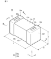
- FIG. 1 is an external perspective view showing an example of a two-terminal multilayer ceramic capacitor as a multilayer ceramic electronic component according to a first embodiment of the present invention.
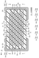
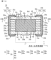
- FIG. 2 is a sectional view taken along line II-II in FIG. 1;
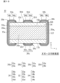
- FIG. 2 is a cross-sectional view taken along line III-III in FIG. 1;
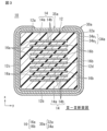
- 3 is a cross-sectional view taken along line IV-IV in FIG. 2.
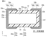
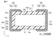
- FIG. 3 is a sectional view taken along line VV in FIG. 2.
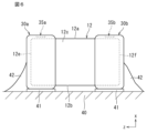
- FIG. FIG. 2 is a side view showing an example of a two-terminal multilayer ceramic capacitor mounted on a mounting board using solder.
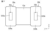
- FIG. 6 is an explanatory diagram for explaining a first example calculation method of exposed area.
- FIG. 6 is an explanatory diagram for explaining a first example calculation method of exposed area.
- FIG. 7 is an explanatory diagram for explaining a second example calculation method of exposed area.
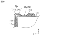
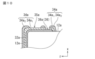
- FIG. 3 is a partial cross-sectional view showing an aspect in which a base electrode layer is exposed.
- FIG. 7 is a partial cross-sectional view showing another embodiment in which a base electrode layer is exposed.
- FIG. 7 is an external perspective view showing an example of a three-terminal multilayer ceramic capacitor according to a second embodiment of the invention.
- FIG. 7 is a top view showing an example of a three-terminal multilayer ceramic capacitor according to a second embodiment of the invention.
- FIG. 7 is a front view showing an example of a three-terminal multilayer ceramic capacitor according to a second embodiment of the invention.
- 12 is a sectional view taken along line XIV-XIV in FIG. 11.
- FIG. 11 is a sectional view taken along line XIV-XIV in FIG. 11.
- FIG. 12 is a sectional view taken along line XV-XV in FIG. 11.
- FIG. 15 is a cross-sectional view taken along line XVI-XVI in FIG. 14.
- FIG. 15 is a sectional view taken along line XVII-XVII in FIG. 14.
- Two-terminal multilayer ceramic capacitor will be described as an example of the multilayer ceramic electronic component according to the first embodiment of the present invention.
- FIG. 1 is an external perspective view showing an example of a two-terminal multilayer ceramic capacitor as a multilayer ceramic electronic component according to a first embodiment of the present invention.
- FIG. 2 is a sectional view taken along line II-II in FIG.
- FIG. 3 is a cross-sectional view taken along line III--III in FIG.
- FIG. 4 is a cross-sectional view taken along line IV-IV in FIG.
- FIG. 5 is a cross-sectional view taken along line VV in FIG.
- the two-terminal multilayer ceramic capacitor 10 includes a rectangular parallelepiped-shaped laminate 12 and external electrodes 30 arranged at both ends of the laminate 12.
- the laminate 12 has a first main surface 12a and a second main surface 12b facing in the height direction x (stacking direction), and a second main surface 12b facing in the width direction y orthogonal to the height direction x. It has a first side surface 12c and a second side surface 12d, and a first end surface 12e and a second end surface 12f that face each other in the length direction z orthogonal to the height direction x and the width direction y.
- the laminate 12 of this embodiment has rounded corners and ridgelines. Note that the corner portion refers to a portion where three adjacent surfaces of the laminate 12 intersect, and the ridgeline portion refers to a portion where two adjacent surfaces of the laminate 12 intersect. In addition, irregularities are formed on part or all of the first main surface 12a and the second main surface 12b, the first side surface 12c and the second side surface 12d, and the first end surface 12e and the second end surface 12f. may have been done.
- the laminate 12 includes an outer layer part 14a made up of a plurality of ceramic layers 14, and an inner layer part 14b made up of one or more ceramic layers 14 and a plurality of internal electrode layers 16 disposed thereon. and, including.
- the outer layer portion 14a is located on the first main surface 12a side and the second main surface 12b side of the laminate 12.
- the outer layer portion 14a includes a plurality of ceramic layers 14 (first outer layer portion) located between the first main surface 12a and the internal electrode layer 16 closest to the first main surface 12a, and a second It is an assembly of a plurality of ceramic layers 14 (second outer layer portion) located between the main surface 12b and the internal electrode layer 16 closest to the second main surface 12b.
- the region sandwiched between both outer layer portions 14a is inner layer portion 14b.
- the ceramic layers 14 and the internal electrode layers 16 are alternately stacked in the height direction x.
- the portion of the stacked body 12 that is sandwiched between the first outer layer portion and the second outer layer portion and where the later-described first internal electrode layer 16a and the later-described second internal electrode layer 16b face each other is referred to as This is called the opposing part (effective layer part).
- the portion between the opposing portion and the first side surface 12c and the portion between the opposing portion and the second side surface 12d are also referred to as a W gap or a side gap.
- a portion including one of the extraction electrode portions is also referred to as an L gap or an end gap.
- the dimensions of the laminate 12 are not particularly limited.
- the dielectric material forming the ceramic layer 14 for example, a dielectric ceramic containing components such as BaTiO 3 , CaTiO 3 , SrTiO 3 , or CaZrO 3 can be used.
- a sub-container with a smaller content than the main component such as a Mn compound, Fe compound, Cr compound, Co compound, Ni compound, etc. You may use the one with added components.
- the laminated ceramic electronic component functions as a piezoelectric component.
- piezoelectric ceramic materials include PZT (lead zirconate titanate) ceramic materials.
- semiconductor ceramic materials include, for example, spinel-based ceramic materials.
- magnetic ceramic materials include ferrite ceramic materials.
- the thickness of the ceramic layer 14 after firing is preferably 0.35 ⁇ m or more and 0.60 ⁇ m or less.
- the number of ceramic layers 14 to be laminated is preferably 10 or more and 2000 or less. Note that the number of ceramic layers 14 is the number of ceramic layers 14 in the inner layer portion 14b, and the number of ceramic layers 14 in the outer layer portion 14a on the first main surface 12a side and the outer layer portion 14a on the second main surface 12b side. This is the total number of
- the laminate 12 includes, as the plurality of internal electrode layers 16, a plurality of first internal electrode layers 16a drawn out to the first end surface 12e and a plurality of second internal electrode layers 16b drawn out to the second end surface 12f. .
- the plurality of first internal electrode layers 16a and the plurality of second internal electrode layers 16b are alternately arranged at equal intervals along the height direction x of the laminate 12 with the ceramic layer 14 in between in the inner layer portion 14b. It is buried like this.
- the surfaces of the plurality of first internal electrode layers 16a and the plurality of second internal electrode layers 16b are generally parallel to the first main surface 12a and the second main surface 12b, and are, for example, approximately rectangular in plan view. It is the shape.
- the first internal electrode layer 16a is arranged on the plurality of ceramic layers 14 and located inside the laminate 12.
- the first internal electrode layer 16a is located at one end side of the first internal electrode layer 16a, and has a first opposing electrode section 26a facing the second internal electrode layer 16b.
- the first lead-out electrode portion 28a extends to the first end surface 12e of the laminate 12.
- the end portion of the first extraction electrode portion 28a is drawn out to the surface of the first end face 12e and exposed from the laminate 12. That is, the first extraction electrode portion 28a is not exposed on the first main surface 12a, the second main surface 12b, the first side surface 12c, the second side surface 12d, and the second end surface 12f.
- the end portion of the first counter electrode portion 26a is located so as to be recessed in the width direction from the surface of the second end face 12f.
- the shape of the first opposing electrode portion 26a of the first internal electrode layer 16a is not particularly limited, but is preferably rectangular in plan view.
- the corner portions may be rounded in plan view, or the corner portions may be formed obliquely in plan view (tapered shape). Alternatively, it may have a tapered shape in plan view with an inclination toward either direction.
- the shape of the first extraction electrode portion 28a of the first internal electrode layer 16a is not particularly limited, but is preferably rectangular in plan view.
- the corner portions may be rounded in plan view, or the corner portions may be formed obliquely in plan view (tapered shape). Alternatively, it may have a tapered shape in plan view with an inclination toward either direction.
- the width of the first counter electrode part 26a of the first internal electrode layer 16a and the width of the first extraction electrode part 28a of the first internal electrode layer 16a may be formed to have the same width, or One width may be formed narrower.
- the second internal electrode layer 16b is arranged on the plurality of ceramic layers 14 and located inside the laminate 12.
- the second internal electrode layer 16b is located at one end side of the second internal electrode layer 16b, and has a second opposing electrode section 26b facing the first internal electrode layer 16a. It has a second extraction electrode portion 28b extending up to the second end surface 12f of the laminate 12.
- the end of the second extraction electrode portion 28b is drawn out to the surface of the second end face 12f and exposed from the laminate 12. That is, the second extraction electrode portion 28b is not exposed on the first main surface 12a, the second main surface 12b, the first side surface 12c, the second side surface 12d, and the first end surface 12e.
- the end portion of the second counter electrode portion 26b is located so as to be recessed in the width direction from the surface of the first end surface 12e.
- the shape of the second opposing electrode portion 26b of the second internal electrode layer 16b is not particularly limited, but is preferably rectangular in plan view.
- the corner portions may be rounded in plan view, or the corner portions may be formed obliquely in plan view (tapered shape). Alternatively, it may have a tapered shape in plan view with an inclination toward either direction.
- the shape of the second extraction electrode portion 28b of the second internal electrode layer 16b is not particularly limited, but is preferably rectangular in plan view.
- the corner portions may be rounded in plan view, or the corner portions may be formed obliquely in plan view (tapered shape). Alternatively, it may have a tapered shape in plan view with an inclination toward either direction.
- the width of the second counter electrode part 26b of the second internal electrode layer 16b and the width of the second extraction electrode part 28b of the second internal electrode layer 16b may be formed to have the same width, or One width may be formed narrower.
- the first internal electrode layer 16a and the second internal electrode layer 16b are made of, for example, a metal such as Ni, Cu, Ag, Pd, or Au, or an alloy containing at least one of these metals such as an Ag-Pd alloy. It can be constructed from any suitable conductive material. Furthermore, when simultaneously firing an integral body including the laminate 12 including the internal electrode layer 16 and the external electrode 30 on the surface of the laminate 12, the metal constituting the internal electrode layer 16 is a compound of the metal contained in the external electrode 30. Configure.
- each of the internal electrode layers 16, that is, the first internal electrode layer 16a and the second internal electrode layer 16b is preferably 0.40 ⁇ m or more and 0.50 ⁇ m or less. Further, the total number of first internal electrode layers 16a and second internal electrode layers 16b is preferably 10 or more and 2000 or less.
- External Electrode External electrodes 30 are arranged on the first end surface 12e side and the second end surface 12f side of the laminate 12, as shown in FIGS. 1 to 3.
- the external electrode 30 has a first external electrode 30a and a second external electrode 30b.
- the first external electrode 30a is connected to the first internal electrode layer 16a and is disposed on at least the surface of the first end surface 12e. In this case, the first external electrode 30a is electrically connected to the first extraction electrode section 28a of the first internal electrode layer 16a. In the present embodiment, the first external electrode 30a extends from the first end surface 12e of the laminate 12 and covers a part of the first main surface 12a, a part of the second main surface 12b, and the first It is also arranged on a part of the side surface 12c and a part of the second side surface 12d.
- the second external electrode 30b is connected to the second internal electrode layer 16b and is disposed on at least the surface of the second end surface 12f.
- the second external electrode 30b is electrically connected to the second extraction electrode section 28b of the second internal electrode layer 16b.
- the second external electrode 30b extends from the second end surface 12f and covers a portion of the first main surface 12a, a portion of the second main surface 12b, and the first side surface 12c. It is also arranged in a part and a part of the second side surface 12d.
- the first opposing electrode portion 26a of the first internal electrode layer 16a and the second opposing electrode portion 26b of the second internal electrode layer 16b are opposed to each other with the ceramic layer 14 in between. , a capacitance is formed. Therefore, capacitance cannot be obtained between the first external electrode 30a to which the first internal electrode layer 16a is connected and the second external electrode 30b to which the second internal electrode layer 16b is connected. , the characteristics of the capacitor are expressed.
- the external electrode 30 is composed of a base electrode layer 32 and a plating layer 34.
- the external electrode 30 includes a base electrode layer 32 containing a metal component and a plating layer 34 disposed on the base electrode layer 32.
- the plating layer 34 includes a first plating layer 34a and a second plating layer 34b.
- the first external electrode 30a includes a first base electrode layer 32a containing a metal component, a first lower plating layer 34a1 disposed on the first base electrode layer 32a, and a first lower plating layer 34a. 1, a first upper plating layer 34a 2 disposed on top of the first upper plating layer 34a 2 .
- the first external electrode 30a has a first plating exposed region 35a exposed on the surface of the first external electrode 30a.
- the second external electrode 30b includes a second base electrode layer 32b containing a metal component, a second lower plating layer 34b1 disposed on the second base electrode layer 32b, and a second lower plating layer 34b. 1 and a second upper plating layer 34b 2 disposed on top of the second upper plating layer 34b 2 . Further, the second external electrode 30b has a second plating exposed region 35b exposed on the surface of the second external electrode 30b.
- the first base electrode layer 32a is connected to the first internal electrode layer 16a and disposed on the surface of the first end surface 12e. In this case, the first base electrode layer 32a is electrically connected to the first extraction electrode portion 28a of the first internal electrode layer 16a. In the present embodiment, the first base electrode layer 32a extends from the first end surface 12e to cover a portion of the first main surface 12a, a portion of the second main surface 12b, and the first side surface 12c. and a portion of the second side surface 12d.
- the second base electrode layer 32b is connected to the second internal electrode layer 16b and arranged on the surface of the second end surface 12f.
- the second base electrode layer 32b is electrically connected to the second extraction electrode portion 28b of the second internal electrode layer 16b.
- the second base electrode layer 32b extends from the second end surface 12f to cover a portion of the first main surface 12a, a portion of the second main surface 12b, and the first side surface 12c. and a portion of the second side surface 12d.
- the base electrode layer 32 includes at least one selected from a baked layer, a conductive resin layer, a thin film layer, and the like.
- a baked layer a baked layer
- a conductive resin layer a thin film layer
- each structure when the base electrode layer 32 is made of the above-mentioned baked layer, conductive resin layer, or thin film layer will be explained.
- the baking layer includes a glass component and a metal component.
- the glass component of the baking layer contains at least one selected from B, Si, Ba, Mg, Al, Li, and the like.
- the metal component of the baking layer includes, for example, at least one selected from Cu, Ni, Ag, Pd, Ag-Pd alloy, Au, and the like.
- the baking layer may be a plurality of layers. The baked layer is obtained by coating and baking a conductive paste containing a glass component and a metal component on the laminate 12, and may be baked simultaneously with the internal electrode layer 16 and the ceramic layer 14. It may be baked after layer 14 is baked.
- the baked layer when the baked layer is fired at the same time as the internal electrode layer 16 and the ceramic layer 14, it is preferable to form the baked layer by adding a ceramic component instead of the glass component.
- the ceramic component the same type of ceramic material as the ceramic layer 14 may be used, or a different type of ceramic material may be used.
- the ceramic component includes, for example, at least one selected from BaTiO 3 , CaTiO 3 , (Ba,Ca)TiO 3 , SrTiO 3 , CaZrO 3 , and the like.
- the glass component or the ceramic component in the baked layer, it is possible to improve the adhesion between the laminate 12 and the base electrode layer 32, which is the baked layer.
- the baked layer may contain both a glass component and a ceramic component.
- the thickness of the first and second baked layers at the central portions in the height direction x of the first and second base electrode layers 32a and 32b located on the first end surface 12e and the second end surface 12f is, for example, 3 ⁇ m or more. The thickness is preferably about 20 ⁇ m or less. Further, in the case where the base electrode layer 32 is provided on the first main surface 12a and the second main surface 12b, the first side surface 12c and the second main surface 12d, the first main surface 12a and the second main surface 12b are Thickness of the first and second baked layers at the center in the length direction z, which are the first and second base electrode layers 32a and 32b located on the surface 12b, the first side surface 12c, and the second side surface 12d. is preferably about 1 ⁇ m or more and 20 ⁇ m or less, for example.
- the conductive resin layer may have multiple layers.
- the conductive resin layer may be placed on the baking layer so as to cover the baking layer, or the conductive resin layer may be placed directly on the laminate 12.
- the conductive resin layer is placed so as to cover the base electrode layer 32, which is the baked layer.
- the conductive resin layer includes a first conductive resin layer and a second conductive resin layer. The first conductive resin layer is arranged to cover the first base electrode layer 32a, and the second conductive resin is arranged to cover the second base electrode layer 32b.
- the first and second conductive resin layers are arranged on the first base electrode layer 32a and the second base electrode layer 32b located on the first end surface 12e and the second end surface 12f. has been done. Further, the first and second conductive resin layers are arranged so as to extend over the first main surface 12a and the second main surface 12b, as well as the first side surface 12c and the second side surface 12d. Preferably. However, the first and second conductive resin layers are arranged only on the first base electrode layer 32a and the second base electrode layer 32b located on the first end surface 12e and the second end surface 12f. You can. Note that when the external electrode 30 has the plating layer 34, the conductive resin layer can be placed between the base electrode layer 32 and the plating layer 34.
- the conductive resin layer contains a thermosetting resin and a metal. Since the conductive resin layer contains a thermosetting resin, it is more flexible than a conductive layer made of, for example, a plated film or a fired product of conductive paste. Therefore, even if the two-terminal multilayer ceramic capacitor 10 is subjected to physical shock or shock due to thermal cycles, the conductive resin layer functions as a buffer layer, and the two-terminal multilayer ceramic capacitor 10 can prevent cracks.
- the metal contained in the conductive resin layer Ag, Cu, Ni, Sn, Bi, or an alloy containing them can be used.
- metal powder whose surface is coated with Ag can also be used.
- metal powder whose surface is coated with Ag it is preferable to use Cu, Ni, Sn, Bi, or alloy powder thereof as the metal powder.
- the reason why conductive metal powder of Ag is used as a conductive metal is that Ag has the lowest specific resistance among metals, making it suitable for electrode materials, and because Ag is a noble metal, it does not oxidize and has high weather resistance. be.
- Ag-coated metal powder is used is that it is possible to use an inexpensive base metal while maintaining the above-mentioned properties of Ag.
- metal contained in the conductive resin layer Cu or Ni subjected to oxidation prevention treatment can also be used.
- metal powder whose surface is coated with Sn, Ni, or Cu can also be used.
- Ag, Cu, Ni, Sn, Bi, or an alloy powder thereof it is preferable to use Ag, Cu, Ni, Sn, Bi, or an alloy powder thereof as the metal powder.
- the metal contained in the conductive resin layer is preferably contained in an amount of 35 vol% or more and 75 vol% or less based on the volume of the entire conductive resin.
- the average particle size of the metal contained in the conductive resin layer is not particularly limited.
- the average particle size of the conductive filler may be, for example, about 0.3 ⁇ m or more and 10 ⁇ m or less.
- the metal contained in the conductive resin layer is mainly responsible for the conductivity of the conductive resin layer. Specifically, when the conductive fillers come into contact with each other, a current-carrying path is formed inside the conductive resin layer.
- the shape of the metal contained in the conductive resin layer is not particularly limited, and shapes such as spherical shape and flat shape can be used.
- the metal contained in the conductive resin layer it is preferable to use a mixture of spherical metal powder and flat metal powder.
- thermosetting resins such as epoxy resin, phenoxy resin, phenol resin, urethane resin, silicone resin, and polyimide resin can be used.
- epoxy resin is one of the most suitable resins because of its excellent heat resistance, moisture resistance, and adhesion.
- the resin contained in the conductive resin layer is preferably contained in an amount of 25 vol% or more and 65 vol% or less with respect to the total volume of the conductive resin.
- the conductive resin layer contains a curing agent together with the thermosetting resin.
- a curing agent such as phenol, amine, acid anhydride, imidazole, active ester, and amide-imide compounds can be used as the curing agent for the epoxy resin. can do.
- the thickness of the conductive resin layer located at the center in the height direction x of the laminate 12 on the first end surface 12e and the second end surface 12f is preferably, for example, about 3 ⁇ m or more and 30 ⁇ m or less.
- the first main surface 12a and the second main surface 12b are also provided on the first main surface 12a and the second main surface 12b, the first side surface 12c and the second side surface 12d, the first main surface 12a and the second main surface 12b are
- the thickness of the conductive resin layer at the center in the length direction z of the conductive resin layer located on the main surface 12b, the first side surface 12c, and the second side surface 12d may be, for example, about 3 ⁇ m or more and 30 ⁇ m or less. preferable.
- the thin film layer is formed by a thin film forming method such as a sputtering method or a vapor deposition method, and is a layer with a thickness of 1 ⁇ m or less on which metal particles are deposited.
- This plating layer 34 has a plating exposed area 35.
- the first plating layer 34a is arranged to cover the first base electrode layer 32a on the first end surface 12e side. Further, the first plating layer 34a is arranged to cover the first base electrode layer 32a on the first main surface 12a, the second main surface 12b, the first side surface 12c, and the second side surface 12d. You can leave it there. However, the first plating layer 34a may be disposed only on the first base electrode layer 32a on the first end surface 12e side.
- the first plating layer 34a includes a first lower plating layer 34a 1 disposed on the first base electrode layer 32a and a first upper plating layer disposed on the first lower plating layer 34a 1 . 34a 2 .
- the first upper plating layer 34a 2 is arranged on the first lower plating layer 34a 1 so as to expose a part of the first lower plating layer 34a 1 . That is, the first upper plating layer 34a 2 has a first plating exposed region such that the first lower plating layer 34a 1 has a first plating exposed region 35a exposed on the surface of the first external electrode 30a. They are arranged on the first lower plating layer 34a 1 except for 35a.
- the first plating exposed region 35a is arranged on the first main surface 12a.
- the second main surface 12b of the two-terminal multilayer ceramic capacitor 10 becomes a mounting surface on the mounting board 40.
- FIG. 6 is a side view showing an example of a two-terminal multilayer ceramic capacitor mounted using solder.
- a pair of planar lands 41 for mounting the two-terminal multilayer ceramic capacitor 10 are formed on the mounting board 40.
- the two-terminal multilayer ceramic capacitor 10 has a second main surface 12b facing the mounting surface of the mounting board 40, and a first main surface 12a on each of the pair of lands 41, with the first main surface 12a being farthest from the mounting surface. are arranged so that the external electrode 30a and the second external electrode 30b are located. In this state, the two-terminal multilayer ceramic capacitor 10 is mounted on the mounting board 40 by applying solder 42 to the first end surface 12e and the second end surface 12f.
- the first upper plating layer 34a 2 covers the end of the first lower plating layer 34a 1 .
- the tip of the first lower plating layer 34a 1 on the second end surface 12f side is covered by the tip of the first upper plating layer 34a 2 on the second end surface 12f side.
- peeling of the first lower plating layer 34a 1 can be suppressed.
- the first ratio of the area of the first plating exposed region 35a to the area of the exposed region of the first external electrode 30a on the first main surface 12a when viewed from the height direction x of the laminate 12 is 0. It is preferably 4% or more and 83.4% or less. Since the first ratio is 0.4% or more, for example, the first and second internal electrode layers 16a and 16b, the first and second base electrode layers 32a and 32b, and the first and second lower plating layers Hydrogen released from 34a 1 and 34b 1 can be sufficiently released from the first plating exposed region 35a to the outside of the two-terminal multilayer ceramic capacitor 10, and deterioration of insulation resistance due to hydrogen can be suppressed.
- the first ratio is 83.4% or less, it is possible to suppress the ratio of the first lower plating layer 34a 1 not covered by the first upper plating layer 34a 2 . Thereby, it is possible to suppress a decrease in moisture resistance due to water vapor intrusion into the two-terminal multilayer ceramic capacitor 10 from the first plating exposed region 35a. More preferably, the first ratio is 1.17% or more and 83.4% or less. More preferably, the first ratio is 1.40% or more and 83.4% or less. More preferably, the first ratio is 1.40% or more and 25.0% or less.
- the first ratio can be determined as follows. First, the area of the exposed region of the first external electrode 30a can be determined from the area of the region where the first external electrode 30a faces the outside of the two-terminal multilayer ceramic capacitor 10. For example, the area of the exposed region of the first external electrode 30a is equal to It can be determined from the area of the region where the external electrode 30a faces the outside of the two-terminal multilayer ceramic capacitor 10. Further, the area of the first plating exposed region 35a can be determined from the area of the region where the first lower plating layer 34a 1 faces the outside of the two-terminal multilayer ceramic capacitor 10.
- the area of the first plating exposed region 35a is equal to the area of the first lower layer plating on the first main surface 12a, the second main surface 12b, the second end surface 12f, the first side surface 12c, and the second side surface 12d. It can be determined from the area of the region where the layer 34a 1 faces the outside of the two-terminal multilayer ceramic capacitor 10. Then, the first ratio can be determined from the ratio of the area of the first plating exposed region 35a to the area of the exposed region of the first external electrode 30a.
- the area S30a of the exposed region of the first external electrode 30a is ), the first external electrode 30a (first base electrode layer 32a, first lower plating layer 34a 1 , first upper plating layer 34a 2 ) is of a two-terminal type on the first main surface 12a It can be determined from the area facing the outside of the multilayer ceramic capacitor 10.
- the area S35a of the first plating exposed region 35a is equal to It can be determined from the region where the first lower plating layer 34a 1 faces the outside of the two-terminal multilayer ceramic capacitor 10 on all sides. Note that FIG.
- the first ratio can be determined from the ratio of the area S35a of the first plating exposed region 35a to the area S30a of the exposed region of the first external electrode 30a.
- the area S30a and the area S35a can be observed using, for example, a microscope (for example, VHX series (hereinafter referred to as VHX) manufactured by Keyence Corporation) at a magnification of 200 times and in a bright field.
- VHX VHX series
- the first ratio can be determined as follows as a second example.
- the area of the exposed region of the first external electrode 30a is determined in the same manner as in the first example.
- the first lower plating layer 34a 1 is also scraped in addition to the first upper plating layer 34a 2 , the first plating exposed area 35a is on the first main surface 12a, the second main surface 12b, When intersecting the first end surface 12e, the first side surface 12c, or the second side surface 12d, the area of the first plating exposed region 35a is the area of the exposed first lower plating layer 34a 1. It can be determined by multiplying the thickness by the circumferential length of the first plating exposed area 35a. Then, the first ratio can be determined from the ratio of the area of the first plating exposed region 35a to the area of the exposed region of the first external electrode 30a.
- the area S30a of the exposed region of the first external electrode 30a is (in a direction view), it can be determined from the region of the first main surface 12a where the first external electrode 30a faces the outside of the two-terminal multilayer ceramic capacitor 10.
- the area SS35a of the first plating exposed region 35a is such that the first plating exposed region 35a is the first main surface 12a, the second main surface 12b, the first end surface 12e, the first side surface 12c, or the second , the thickness t35a of the exposed first lower plating layer 34a 1 and the circumferential length of the first plating exposed area 35a (l35a 1 , l35a 2 , l35a 3 , l35a 4 ).
- FIG. 8 shows, as an example, a mode in which the first plating exposed region 35a intersects with the first main surface 12a.
- the first ratio can be determined from the ratio of the area SS35a of the first plating exposed region 35a to the area S30a of the exposed region of the first external electrode 30a.
- the lengths l35a 1 to l35a 4 can be observed using, for example, a microscope (VHX) at a magnification of 200 times and in a bright field.
- the thickness t35a can be determined by polishing the cross section to, for example, 1/2 of the W dimension in the width direction y of the two-terminal multilayer ceramic capacitor 10, and then using a microscope (VHX) at a magnification of 2000 times and bright field. It can be observed at.
- the second plating layer 34b is arranged to cover the second base electrode layer 32b on the second end surface 12f side. Further, the second plating layer 34b is arranged to cover the second base electrode layer 32b on the first main surface 12a, the second main surface 12b, the first side surface 12c, and the second side surface 12d. You can leave it there. However, the second plating layer 34b may be disposed only on the second base electrode layer 32b on the second end surface 12f side.
- This second plating layer 34b includes a second lower plating layer 34b 1 disposed on the second base electrode layer 32b and a second upper plating layer disposed on the second lower plating layer 34b 1 . 34b 2 .
- the second upper plating layer 34b 2 is arranged on the second lower plating layer 34b 1 so as to expose a part of the second lower plating layer 34b 1 . That is, the second upper plating layer 34b 2 has a second plating exposed region such that the second lower plating layer 34b 1 has a second plating exposed region 35b exposed on the surface of the second external electrode 30b. They are arranged on the second lower plating layer 34b 1 except for 35b. In this embodiment, the second plating exposed region 35b is arranged on the first main surface 12a. In this case, the second main surface 12b of the two-terminal multilayer ceramic capacitor 10 becomes a mounting surface on the mounting board.
- the second upper plating layer 34b 2 covers the end of the second lower plating layer 34b 1 .
- the tip of the second lower plating layer 34b 1 on the first end surface 12e side is covered by the tip of the second upper plating layer 34b 2 on the first end surface 12e side.
- peeling of the second lower plating layer 34b 1 can be suppressed.
- the second plating exposed area 35b is relative to the area of the exposed area of the second external electrode 30b on the first main surface 12a when viewed from the height direction x of the laminate 12.
- the second ratio of the area of is preferably 0.4% or more and 83.4% or less. Since the second ratio is 0.4% or more, for example, the first and second internal electrode layers 16a and 16b, the first and second base electrode layers 32a and 32b, and the first and second lower plating layers Hydrogen released from 34a 1 and 34b 1 can be sufficiently released from the second plating exposed region 35b to the outside of the two-terminal multilayer ceramic capacitor 10, and deterioration of insulation resistance due to hydrogen can be suppressed.
- the second ratio is 83.4% or less, it is possible to suppress a decrease in moisture resistance due to water vapor intrusion into the two-terminal multilayer ceramic capacitor 10 from the second plating exposed region 35b. More preferably, the second ratio is 1.17% or more and 83.4% or less. More preferably, the second ratio is 1.40% or more and 83.4% or less. More preferably, the second ratio is 1.40% or more and 25.0% or less.
- the second ratio can be determined in the same way as the first ratio.
- the area of the exposed region of the second external electrode 30b is equal to Determined from the area of the region where the external electrode 30b (second base electrode layer 32b, second lower plating layer 34b 1 , second upper plating layer 34b 2 ) faces the outside of the two-terminal multilayer ceramic capacitor 10 be able to.
- the area of the second plating exposed region 35b is the area of the first main surface 12a, the second main surface 12b, the second end surface 12f, the first side surface 12c, and the second side surface 12d. It can be determined from the area of the region where the second lower plating layer 34b 1 faces the outside of the two-terminal multilayer ceramic capacitor 10 when viewed from all sides.
- the area of the exposed region of the second external electrode 30b can be determined in the same manner as in the first example.
- the area of the second plating exposed region 35b is such that the second plating exposed region 35b is located between the first main surface 12a, the second main surface 12b, the second end surface 12f, and the first side surface. 12c or the second side surface 12d, find it from the area multiplied by the thickness of the exposed second lower plating layer 34b1 and the circumference of the second plating exposed region 35b. I can do it.
- the second ratio can be determined from the ratio of the area of the second plating exposed region 35b to the area of the exposed region of the second external electrode 30b.
- the first ratio and the second ratio are respectively calculated as the exposure ratio. It may be a ratio of the total area of the plating exposed region 35a and the second plating exposed region 35b.
- the total exposure ratio is preferably 0.4% or more and 83.4% or less.
- the first plating layer 34a and the second plating layer 34b include, for example, at least one selected from Cu, Ni, Sn, Ag, Pd, Ag-Pd alloy, Au, and the like.
- first lower plating layer 34a 1 and the second lower plating layer 34b 1 are Ni plating layers
- first upper plating layer 34a 2 and the second upper plating layer 34b 2 are Sn plating layers.
- the first and second lower plating layers 34a 1 and 34b 1 made of Ni plating layers are used to prevent the base electrode layer 32 from being eroded by solder when mounting the two-terminal multilayer ceramic capacitor 10. .
- the first and second upper plating layers 34a 2 and 34b 2 made of Sn plating layers improve the wettability of solder when mounting the two-terminal multilayer ceramic capacitor 10, making it possible to easily mount the capacitor 10. It is used to make things happen.
- the thickness is preferably 2 ⁇ m or more and 7 ⁇ m or less.
- the first main surface 12a, the second main surface 12b, the second end surface 12f, the first side surface 12c, and the second side surface 12d of the second lower plating layer 34b 1 and the second upper plating layer 34b 2 The thickness is preferably 2 ⁇ m or more and 7 ⁇ m or less.
- the plating layer 34 is arranged to cover the conductive resin layer.
- the Ni plating layer which is the lower plating layer of the plating layer 34, prevents the conductive resin layer from being eroded by solder
- the Sn plating layer which is the upper plating layer, improves solder wettability.
- the dimension in the longitudinal direction z of the 2-terminal multilayer ceramic capacitor 10 including the multilayer body 12, the first external electrode 30a, and the second external electrode 30b is L dimension, and the multilayer The dimension in the height direction x of the two-terminal multilayer ceramic capacitor 10 including the body 12, the first external electrode 30a, and the second external electrode 30b is the T dimension, and the multilayer body 12, the first external electrode 30a, and the second The dimension in the width direction y of the two-terminal multilayer ceramic capacitor 10 including the external electrode 30b is defined as the W dimension.
- the dimensions of the two-terminal multilayer ceramic capacitor 10 are as follows: L dimension in the length direction z is 0.2 mm or more and 6.5 mm or less, W dimension in the width direction y is 0.1 mm or more and 5.5 mm or less, and T in the height direction x. The dimensions are 0.1 mm or more and 6.5 mm or less. Further, the dimensions of the two-terminal multilayer ceramic capacitor 10 can be measured using a microscope.
- Step 1 a dielectric sheet for the ceramic layer 14 and a conductive paste for the internal electrode layer 16 are prepared.
- the conductive paste for the dielectric sheet and internal electrode layer 16 contains a binder and a solvent.
- the binder and solvent may be known.
- Step 2 a conductive paste for the internal electrode layer 16 is printed in a predetermined pattern on the dielectric sheet by, for example, screen printing or gravure printing.
- a dielectric sheet on which the pattern of the first internal electrode layer 16a is formed and a dielectric sheet on which the pattern of the second internal electrode layer 16b is formed are prepared.
- a dielectric sheet for an outer layer on which the internal electrode layer pattern is not printed is also prepared.
- Step 3 By laminating a predetermined number of dielectric sheets for the outer layer on which the pattern of the internal electrode layer is not printed, the outer layer portion 14a on the second main surface 12b side is formed (outer layer portion forming step) .
- a dielectric sheet with a pattern of the first internal electrode layer 16a printed on the outer layer portion 14a on the second main surface 12b side and a dielectric sheet with the pattern of the second internal electrode layer 16b printed are printed.
- the inner layer portion 14b is formed by sequentially laminating the layers to form the structure of the invention (inner layer portion forming step). Subsequently, a predetermined number of dielectric sheets for the outer layer on which the pattern of the internal electrode layer is not printed are laminated on the inner layer. As a result, the outer layer portion 14a on the first main surface 12a side is formed on the inner layer portion 14b (outer layer portion forming step).
- Step 4 the laminated sheet is pressed in the lamination direction by means such as a hydrostatic press to produce a laminated block.
- Step 5 the laminated block is cut into a predetermined size to cut out the laminated chip.
- the corners and ridges of the stacked chips may be rounded by barrel polishing or the like.
- Step 6 the stacked chips are fired to produce the stacked body 12.
- the firing temperature is preferably 900° C. or more and 1400° C. or less, although it depends on the materials of the dielectric ceramic layer and the internal electrode layer.
- a base electrode layer 32 is formed by applying a conductive paste for external electrodes to both end surfaces 12e, 12f, etc. of the laminate 12.
- the manufacturing process for each case where the base electrode layer 32 is a baked layer, a conductive resin layer, and a thin film layer will be described below.
- the base electrode layer 32 is a baked layer
- a conductive paste containing a glass component and a metal is applied by a method such as dipping or screen printing, and then a baking process is performed to form the base electrode layer 32. do.
- the baking temperature at this time is preferably 700°C or more and 900°C or less.
- the baked layer may contain a ceramic component instead of the glass component, or may contain both.
- the ceramic component is, for example, the same type of ceramic material as the laminate.
- bake (fire) it is preferable to bake (fire) to form a laminate in which a baked layer is formed.
- the temperature of the baking treatment (firing temperature) at this time is preferably 900°C or more and 1400°C or less.
- the base electrode layer 32 is a conductive resin layer
- a conductive resin paste containing a thermosetting resin and a metal component is applied onto the baking layer or the laminate 12 and heated at a temperature of 250° C. or more and 550° C. or less. Heat treatment is performed to thermoset the resin and form a conductive resin layer.
- the atmosphere during the heat treatment at this time is preferably a N 2 atmosphere. Further, in order to prevent resin scattering and oxidation of various metal components, it is preferable to suppress the oxygen concentration to 100 ppm or less.
- the base electrode layer 32 can be formed by a thin film forming method such as a sputtering method or a vapor deposition method.
- the base electrode layer 32 formed of a thin film layer is a layer with a thickness of 1 ⁇ m or less on which metal particles are deposited.
- a plating layer 34 is formed on the surface of the base electrode layer 32.
- Either electrolytic plating or electroless plating can be used for plating, but electroless plating requires pretreatment with catalysts to improve the plating deposition rate, making the process more complicated. There is a disadvantage. Therefore, it is usually preferable to employ electrolytic plating.
- As the plating method it is preferable to use barrel plating.
- the first lower plating layer 34a 1 and the second lower plating layer 34b 1 are formed as the plating layer 34, and the first upper plating layer 34a 2 and A second upper plating layer 34b 2 (Sn plating layer) is sequentially formed.
- a conductive resin paste containing a resin component and a metal component is prepared, and the conductive resin paste is applied on the base electrode layer 32 using a dipping method. . Thereafter, a plating layer 34 is formed on the conductive resin layer.
- Step 9 the first upper plating layer 34a 2 and the second upper plating layer 34a 1 and the second lower plating layer 34b 1 (Ni plating layer) are exposed at a predetermined exposure ratio.
- the upper plating layer 34b 2 (Sn plating layer) is treated.
- a scraping method for example, a melting method, a method using laser processing, a method using a resist, etc. can be adopted.
- a metal terminal with a diameter of about 30 to 100 ⁇ m is brought into contact with the first upper plating layer 34a 2 and the second upper plating layer 34b 2 (Sn plating layer).
- the soft Sn plating layer is removed so that the lower plating layer 34b 1 (Ni plating layer) of No. 2 has a predetermined exposure ratio.
- the molded body after the plating layer 34 has been formed is immersed in an enstripping agent (release agent). For example, by aligning the heights of the plurality of molded bodies after forming the plating layer 34 using an alignment jig and immersing one side of the molded body in an enstripping agent, the first lower layer plating layer 34a 1 and the second lower layer plating can be formed.
- the first upper plating layer 34a 2 and the second upper plating layer 34b 2 (Sn plating layer) are dissolved so that the layer 34b 1 (Ni plating layer) has a predetermined exposure ratio.
- a plurality of molded bodies after the plating layer 34 has been formed are aligned so that the first lower plating layer 34a 1 and the second lower plating layer 34b 1 (Ni plating layer) have a predetermined exposure ratio.
- first upper plating layer 34a 2 and the second upper plating layer 34b 2 (Sn plating layer) of each molded body is shaved off with a laser.
- the first and second lower plating layers 34a 1 and 34b 1 (Ni plating layers) having a predetermined exposure ratio can also be formed by using a resist.
- the two-terminal multilayer ceramic capacitor 10 according to this embodiment is manufactured as described above.
- hydrogen ions are generated by a chemical reaction. These hydrogen ions may be applied to at least one of the first and second lower plating layers 34a 1 and 34b 1 , the first and second internal electrode layers 16a and 16b, and the first and second base electrode layers 32a and 32b, for example. may be absorbed as hydrogen. According to the above configuration, at least one of the first and second lower plating layers 34a 1 and 34b 1 , the first and second internal electrode layers 16a and 16b, and the first and second base electrode layers 32a and 32b.
- Hydrogen absorbed in the layer can be released to the outside of the two-terminal multilayer ceramic capacitor 10 from the first and second plating exposed regions 35a and 35b. Therefore, hydrogen can be prevented from remaining absorbed in the absorption layer, and deterioration of insulation resistance due to hydrogen can be suppressed.
- the absorption layer contains a metal such as Ni that is difficult to absorb hydrogen, hydrogen can be released from the first and second plating exposed regions 35a and 35b to the outside of the two-terminal multilayer ceramic capacitor 10. Accordingly, deterioration of the insulation resistance of the ceramic layer 14 can be suppressed.
- first and second plating exposed areas 35a and 35b are formed on the first main surface 12a side, and the second main surface 12b side becomes the mounting surface of the two-terminal multilayer ceramic capacitor 10 on the mounting board.
- solder is mainly applied to the first and second end surfaces 12e and 12f
- the first and second plating is applied from the first main surface 12a that is not coated with solder and does not face the mounting board 40. Hydrogen in the absorption layer can be efficiently released through the exposed regions 35a and 35b.
- the external electrode 30 of the first embodiment described above includes a base electrode layer 32 and a plating layer 34. Differently from this, the external electrode 30 may include the plating layer 34 and may not include the base electrode layer 32. Although not shown, a structure in which the plating layer 34 is provided without providing the base electrode layer 32 for the first and second external electrodes 30a and 30b will be described below.
- the base electrode layer 32 may not be provided, and the plating layer 34 may be directly formed on the surface of the laminate 12. That is, the two-terminal multilayer ceramic capacitor 10 has a first end surface 12e and a second end surface 12f subjected to plating treatment, and is electrically connected to the first internal electrode layer 16a or the second internal electrode layer 16b.
- a structure in which a plating layer 34 is formed may also be used. In such a case, the plating layer 34 may be formed by plating after disposing a catalyst on the surface of the laminate 12 as a pretreatment. In performing the plating treatment, either electrolytic plating or electroless plating may be employed.
- electroless plating requires pretreatment with a catalyst or the like in order to improve the plating deposition rate, which has the disadvantage of complicating the process. Therefore, it is usually preferable to employ electrolytic plating.
- the plating method it is preferable to use barrel plating.
- the thickness of the base electrode layer 32 is reduced by reducing the height, that is, the thickness, or the thickness of the laminate, that is, the effective layer. Since the thickness of the laminate 12 can be changed to the thickness of the laminate 12, the degree of freedom in designing the thickness of the laminate 12 can be improved.
- the plating layer 34 includes first and second lower plating layers 34a 1 and 34b 1 (lower plating layers) formed on the surface of the laminate 12, and first and second lower plating layers 34a 1 and 34b 1 . It includes first and second upper plating layers 34a 2 and 34b 2 (upper plating layers) formed on the surface.
- the lower plating layer has an exposed plating area that is not covered by the upper plating layer, similar to the above embodiment. It is preferable that the lower plating layer and the upper plating layer each contain at least one metal selected from, for example, Cu, Ni, Sn, Pb, Au, Ag, Pd, Bi, or Zn, or an alloy containing the metal. Further, the lower plating layer is preferably formed using Ni, which has solder barrier properties, and the upper plating layer is preferably formed using Sn or Au, which has good solder wettability.
- the lower plating layer is formed using Cu, which has good bonding properties with Ni.
- the upper plating layer may be the outermost layer, or another plating electrode may be formed on the surface of the upper plating layer.
- the thickness of each plating layer 34 arranged without providing the base electrode layer 32 is 1.0 ⁇ m or more and 20 ⁇ m or more. It is preferable that it is .0 ⁇ m or less. Furthermore, it is preferable that the plating layer 34 does not contain glass.
- the metal ratio per unit volume of the plating layer 34 is preferably 99% by volume or more.
- the first lower plating layer 34a 1 has the first plating exposed area 35a not covered by the first upper plating layer 34a 2
- the second lower plating layer 34b 1 has a second plating exposed region 35b that is not covered by the second upper plating layer 34b 2
- the aspect of the exposed region is not limited to this, and the external electrode 30 may have a base exposed region 36 in which the base electrode layer 32 is not covered with the plating layer 34.
- the first base electrode layer 32a has a first base exposed region 36a that is not covered with the first plating layer 34a.
- the first exposed base region 36a may be formed in the manner shown in FIGS. 9 and 10, for example.
- a first plating exposed region 35a is formed so that the first main surface 12a side of the first lower plating layer 34a1 is exposed, and a first plating exposed region 35a is formed in this first plating exposed region 35a.
- a base exposed region 36a is formed.
- the first main surface 12a side of the first base electrode layer 32a is not covered with the first lower plating layer 34a 1 and the first upper plating layer 34a 2 and is exposed. ing.
- the first plating exposed area 35a and the first base exposed area 36a are arranged at different positions on the first main surface 12a.
- the first exposed base region 36a is preferably arranged on the first main surface 12a.
- the second main surface 12b is a mounting surface.
- the second main surface 12b other than the first main surface 12a, the first end surface 12e, the first side surface 12c, and the second side surface 12d may be placed in
- first plating exposed region 35a and the first base exposed region 36a may be formed on different surfaces.
- first plating exposed region 35a may be arranged on the first end surface 12e
- first base exposed region 36a may be arranged on the first main surface 12a.
- the first base exposed region 36a is preferably formed closer to the first end surface 12e than the tip of the first lower plating layer 34a 1 on the second end surface 12f side. That is, it is preferable that the tip of the first base electrode layer 32a on the second end surface 12f side is covered by the tip of the first lower plating layer 34a 1 on the second end surface 12f side. Thereby, peeling of the first base electrode layer 32a can be suppressed.
- the first base exposed region 36a is formed using a scraping method, a melting method, a laser processing method, a method using a resist, etc. to form the first lower plating layer 34a 1 and It can be formed by removing the first upper plating layer 34a 2 .
- the second base electrode layer 32b can similarly have a second base exposed region that is not covered by the second plating layer 34b.
- the first plating exposed region 35a where the first lower plating layer 34a 1 is not covered by the first upper plating layer 34a 2 is provided on the first main surface 12a.
- a second plating exposed region 35b where the second lower plating layer 34b 1 is not covered by the second upper plating layer 34b 2 is provided on the first main surface 12a.
- the plating exposed area 35 is not limited to this, and the plating exposed area 35 includes at least the first main surface 12a, the second main surface 12b, the first end surface 12e, the second end surface 12f, the first side surface 12c, and the second side surface 12d. It is sufficient if it is provided in either one.
- the first exposed plating region 35a of the first external electrode 30a and the second exposed plating region 35b of the second external electrode 30b are provided. However, it is sufficient that at least one of the first exposed plating region 35a and the second exposed plating region 35b is provided.
- the first lower plating layer 34a 1 is arranged to cover all of the first base electrode layer 32a, and the second lower plating layer 34b 1 is arranged to cover the entire first base electrode layer 32a. It is arranged so as to cover all of 32b.
- the present invention is not limited thereto, and the first lower plating layer 34a 1 is arranged to cover a part of the first base electrode layer 32a, and the second lower plating layer 34b 1 is arranged to cover a part of the first base electrode layer 32b. It may be arranged so as to partially cover it.
- Second embodiment 1 Three-Terminal Multilayer Ceramic Capacitor A three-terminal multilayer ceramic capacitor will be described as an example of a multilayer ceramic electronic component according to a second embodiment of the present invention.
- FIG. 11 is an external perspective view showing an example of a three-terminal multilayer ceramic capacitor according to the second embodiment of the present invention.
- FIG. 12 is a top view showing an example of a three-terminal multilayer ceramic capacitor according to the second embodiment of the invention.
- FIG. 13 is a front view showing an example of a three-terminal multilayer ceramic capacitor according to the second embodiment of the invention.
- FIG. 14 is a cross-sectional view taken along line XIV-XIV in FIG.
- FIG. 15 is a cross-sectional view taken along line XV-XV in FIG. 11.
- FIG. 16 is a cross-sectional view taken along line XVI-XVI in FIG. 14.
- FIG. 17 is a cross-sectional view taken along line XVII-XVII in FIG. 14.
- a three-terminal multilayer ceramic capacitor 100 includes, for example, a substantially rectangular parallelepiped-shaped laminate 12 and an external electrode 30.
- the laminated body 12 includes a plurality of laminated ceramic layers 14 and a plurality of internal electrode layers 16 laminated on the ceramic layers 14.
- the ceramic layer 14 and the internal electrode layer 16 are stacked in the height direction x.
- the laminate 12 has a first main surface 12a and a second main surface 12b facing in the height direction x, and a first side surface 12c and a second side surface facing in the width direction y perpendicular to the height direction x. 12d, and a first end surface 12e and a second end surface 12f that face each other in the length direction z perpendicular to the height direction x and the width direction y.
- This laminate 12 has rounded corners and ridges. Note that a corner is a portion where three adjacent surfaces of the laminate intersect, and a ridgeline is a portion where two adjacent surfaces of the laminate intersect.
- first main surface 12a and the second main surface 12b the first side surface 12c and the second side surface 12d, and the first end surface 12e and the second end surface 12f. may have been done.
- the dimension L of the laminate 12 in the length direction z is not necessarily longer than the dimension W in the width direction y.
- the laminate 12 includes an inner layer portion 18, and a first main surface side outer layer portion 20a and a second main surface side outer layer portion 20b, which are arranged to sandwich the inner layer portion 18 in the stacking direction.
- the inner layer portion 18 includes a plurality of ceramic layers 14 and a plurality of internal electrode layers 16.
- the inner layer portion 18 includes an internal electrode layer 16 located closest to the first main surface 12a to an internal electrode layer 16 located closest to the second main surface 12b in the stacking direction.
- the internal electrode layer 16 includes a first internal electrode layer 16a drawn out to a first end surface 12e and a second end surface 12f, and a second internal electrode layer 16b drawn out to a first side surface 12c and a second side surface 12d.
- a plurality of first internal electrode layers 16a and a plurality of second internal electrode layers 16b are opposed to each other with the ceramic layer 14 in between.
- the inner layer portion 18 is a portion that generates capacitance and essentially functions as a capacitor.
- the laminate 12 is located on the first main surface 12a side, and is located between the first main surface 12a and the outermost surface of the inner layer portion 18 on the first main surface 12a side and a straight line on the outermost surface. It has a first main surface side outer layer portion 20a formed from a plurality of ceramic layers 14.
- the first main surface side outer layer portion 20a is an aggregate of a plurality of ceramic layers 14 located between the first main surface 12a and the internal electrode layer 16 closest to the first main surface 12a.
- the ceramic layer 14 used in the first main surface side outer layer portion 20a may be the same as the ceramic layer 14 used in the inner layer portion 18.
- the laminate 12 is located on the second main surface 12b side, and between the second main surface 12b and the outermost surface of the inner layer portion 18 on the second main surface 12b side and a straight line on the outermost surface. It has a second main surface side outer layer portion 20b formed from a plurality of ceramic layers 14 located at .
- the second main surface side outer layer portion 20b is an aggregate of a plurality of ceramic layers 14 located between the second main surface 12b and the internal electrode layer 16 closest to the second main surface 12b.
- the ceramic layer 14 used in the second main surface side outer layer portion 20b may be the same as the ceramic layer 14 used in the inner layer portion 18.
- the laminate 12 is formed from a plurality of ceramic layers 14 located on the first side surface 12c side and located between the first side surface 12c and the outermost surface of the inner layer portion 18 on the first side surface 12c side. It has a first side outer layer portion 22a.
- the laminate 12 is formed from a plurality of ceramic layers 14 located on the second side surface 12d side and located between the second side surface 12d and the outermost surface of the inner layer portion 18 on the second side surface 12d side. It has a second side outer layer portion 22b.
- the first side-side outer layer portion 22a and the second side-side outer layer portion 22b are also referred to as a W gap or a side gap.
- the laminate 12 is formed from a plurality of ceramic layers 14 located on the first end surface 12e side and located between the first end surface 12e and the outermost surface of the inner layer portion 18 on the first end surface 12e side. It has a first end surface side outer layer portion 24a.
- the laminate 12 is formed from a plurality of ceramic layers 14 located on the second end surface 12f side and located between the second end surface 12f and the outermost surface of the inner layer portion 18 on the second end surface 12f side. It has a second end surface side outer layer portion 24b.
- the first end surface side outer layer portion 24a and the second end surface side outer layer portion 24b are also referred to as an L gap or an end gap.
- the dimensions of the laminate 12 are not particularly limited.
- the ceramic layer 14 can be formed of a dielectric material as a ceramic material, for example.
- a dielectric material for example, a dielectric ceramic containing components such as BaTiO 3 , CaTiO 3 , SrTiO 3 , or CaZrO 3 can be used.
- a sub-container with a smaller content than the main component such as a Mn compound, Fe compound, Cr compound, Co compound, Ni compound, etc. You may use the one with added components.
- the thickness of the ceramic layer 14 after firing is preferably 0.35 ⁇ m or more and 0.60 ⁇ m or less.
- the number of ceramic layers 14 to be laminated is preferably 10 or more and 2000 or less. Note that the number of ceramic layers 14 is the total number of ceramic layers 14 in the inner layer section 18 and the number of ceramic layers 14 in the first main surface side outer layer section 20a and the second main surface side outer layer section 20b. be.
- the laminate 12 has a plurality of first internal electrode layers 16a and a plurality of second internal electrode layers 16b as the plurality of internal electrode layers 16.
- the plurality of first internal electrode layers 16a and the plurality of second internal electrode layers 16b may be alternately laminated with the ceramic layers 14 in between, and the ceramic layer on which the first internal electrode layer 16a is arranged After a plurality of ceramic layers 14 are laminated, the ceramic layer 14 on which the second internal electrode layer 16b is arranged may be laminated. In this way, the lamination pattern can be changed depending on the desired capacitance value.
- the first internal electrode layer 16a includes a first opposing electrode section 26a facing the second internal electrode layer 16b, and a first end surface of the stacked body 12 from the first opposing electrode section 26a. 12e, and a second extraction electrode portion 28a 2 that is drawn out from the first opposing electrode portion 26a to the surface of the second end face 12f of the stacked body 12 .
- the first extraction electrode portion 28a 1 is exposed on the surface of the first end surface 12e of the laminate 12
- the second extraction electrode portion 28a 2 is exposed on the surface of the second end surface 12f of the laminate 12. exposed on the surface. Therefore, the first internal electrode layer 16a is not exposed on the surfaces of the first side surface 12c and the second side surface 12d of the stacked body 12.
- the shape of the first opposing electrode section 26a and the shapes of the first extraction electrode section 28a 1 and the second extraction electrode section 28a 2 are not particularly limited, but are preferably rectangular. However, the corner portions may be rounded.
- the length in the width direction y of the first extraction electrode part 28a 1 and the second extraction electrode part 28a 2 may be the same as the length in the width direction y of the first counter electrode part 26a, or may be formed short. You can.
- the shapes of the first extraction electrode part 28a 1 and the second extraction electrode part 28a 2 may be tapered.
- the second internal electrode layer 16b has a substantially cross shape, and is a laminate formed from a second opposing electrode part 26b facing the first internal electrode layer 16a, and a second opposing electrode part 26b.
- the third extraction electrode part 28b1 is drawn out to the surface of the first side surface 12c of the laminate 12
- the fourth extraction electrode part 28b is drawn out from the second opposing electrode part 26b to the surface of the second side surface 12d of the laminate 12. Equipped with 2 .
- the third extraction electrode portion 28b 1 is exposed on the surface of the first side surface 12c of the laminate 12
- the fourth extraction electrode portion 28b 2 is exposed on the surface of the second side surface 12d of the laminate 12. exposed on the surface. Therefore, the second internal electrode layer 16b is not exposed on the surface of the first end surface 12e and the surface of the second end surface 12f of the stacked body 12.
- the shape of the second counter electrode section 26b and the shapes of the third extraction electrode section 28b 1 and the fourth extraction electrode section 28b 2 are rectangular. However, the corner portions may be rounded.
- the relationship between the dimension B in the length direction z connecting the side of the electrode portion 28b 2 on the first end surface 12e side and the side on the second end surface 12f side is preferably A ⁇ B.
- the shape of the third extraction electrode portion 28b 1 may be a tapered shape such that the width becomes narrower toward the first side surface 12c
- the shape of the fourth extraction electrode portion 28b 2 may be a shape similar to that of the second extraction electrode portion 28b 1. It may have a tapered shape in which the width becomes narrower toward the side surface 12d.
- the laminate 12 has a counter electrode part 27.
- the counter electrode part 27 is a part where the first counter electrode part 26a of the first internal electrode layer 16a and the second counter electrode part 26b of the second internal electrode layer 16b face each other.
- the counter electrode section 27 is configured as a part of the inner layer section 18. Note that the counter electrode section 27 is also referred to as a capacitor effective section.
- the first internal electrode layer 16a and the second internal electrode layer 16b are made of, for example, a metal such as Ni, Cu, Ag, Pd, or Au, or an alloy containing at least one of these metals such as an Ag-Pd alloy. It can be constructed from any suitable conductive material.
- first internal electrode layers 16a and second internal electrode layers 16b is not particularly limited, but is preferably about 10 or more and 2000 or less in total, for example.
- the thickness of the first internal electrode layer 16a is, for example, preferably about 0.40 ⁇ m or more and 0.50 ⁇ m or less, although it is not particularly limited.
- the thickness of the second internal electrode layer 16b is, for example, preferably about 0.40 ⁇ m or more and 0.50 ⁇ m or less, although it is not particularly limited.
- External electrode The first end surface 12e side and the second end surface 12f side, the first side surface 12c side and the second side surface 12d side, and the first main surface 12a and second main surface of the laminate 12
- the external electrode 30 is arranged at 12b.
- the external electrode 30 includes a first external electrode 30a, a second external electrode 30b, a third external electrode 30c, and a fourth external electrode 30d.
- the first external electrode 30a is connected to the first internal electrode layer 16a and is arranged on the surface of the first end surface 12e. Further, the first external electrode 30a extends from the first end surface 12e of the laminate 12 and covers a portion of the first main surface 12a, a portion of the second main surface 12b, and the first side surface 12c. It is also arranged in a part and a part of the second side surface 12d. In this case, the first external electrode 30a is electrically connected to the first extraction electrode portion 28a 1 of the first internal electrode layer 16a.
- the second external electrode 30b is connected to the first internal electrode layer 16a and is arranged on the surface of the second end surface 12f. Further, the second external electrode 30b extends from the second end surface 12f of the laminate 12 and covers a portion of the first main surface 12a, a portion of the second main surface 12b, and the first side surface 12c. It is also arranged in a part and a part of the second side surface 12d. In this case, the second external electrode 30b is electrically connected to the second extraction electrode portion 28a 2 of the first internal electrode layer 16a.
- the third external electrode 30c is connected to the second internal electrode layer 16b and arranged on the surface of the first side surface 12c. Further, the third external electrode 30c extends from the first side surface 12c of the stacked body 12 and is also arranged on a portion of the first main surface 12a and a portion of the second main surface 12b. In this case, the third external electrode 30c is electrically connected to the third extraction electrode portion 28b 1 of the second internal electrode layer 16b. Note that the third external electrode 30c may be arranged only on the surface of the first side surface 12c.
- the fourth external electrode 30d is connected to the second internal electrode layer 16b and arranged on the surface of the second side surface 12d. Further, the fourth external electrode 30d extends from the second side surface 12d of the stacked body 12 and is also arranged on a part of the first main surface 12a and a part of the second main surface 12b. In this case, the fourth external electrode 30d is electrically connected to the fourth extraction electrode portion 28b 2 of the second internal electrode layer 16b. Note that the fourth external electrode 30d may be arranged only on the surface of the second side surface 12d.
- the first opposing electrode portion 26a of the first internal electrode layer 16a and the second opposing electrode portion 26b of the second internal electrode layer 16b are opposed to each other with the ceramic layer 14 in between. , a capacitance is formed. Therefore, the first external electrode 30a and the second external electrode 30b are connected to the first internal electrode layer 16a, and the third external electrode 30c and the fourth external electrode are connected to the second internal electrode layer 16b. 30d, a capacitance can be obtained and the characteristics of a capacitor are expressed.
- the external electrode 30 includes a base electrode layer 32 containing a metal component and a glass component, and a plating layer 34 disposed on the surface of the base electrode layer 32.
- the plating layer 34 includes a lower plating layer and an upper plating layer.
- the first external electrode 30a includes a first base electrode layer 32a containing a metal component, a first lower plating layer 34a1 disposed on the first base electrode layer 32a, and a first lower plating layer 34a. 1, a first upper plating layer 34a 2 disposed on top of the first upper plating layer 34a 2 . Further, the first external electrode 30a has a first plating exposed region 35a exposed on the surface of the first external electrode 30a.
- the second external electrode 30b includes a second base electrode layer 32b containing a metal component, a second lower plating layer 34b1 disposed on the second base electrode layer 32b, and a second lower plating layer 34b. 1, a second upper plating layer 34b 2 disposed on top of the second upper plating layer 34b 2 . Further, the second external electrode 30b has a second plating exposed region 35b exposed on the surface of the second external electrode 30b.
- the third external electrode 30c includes a third base electrode layer 32c containing a metal component, a third lower plating layer 34c 1 disposed on the third base electrode layer 32c, and a third lower plating layer 34c. 1 and a third upper plating layer 34c 2 disposed on top of the plating layer 34c 2 .
- the fourth external electrode 30d includes a fourth base electrode layer 32d containing a metal component, a fourth lower plating layer 34d 1 disposed on the fourth base electrode layer 32d, and a fourth lower plating layer 34d. 1 and a fourth upper plating layer 34d 2 disposed on top of the fourth upper plating layer 34d 2 .
- the base electrode layer 32 includes a first base electrode layer 32a, a second base electrode layer 32b, a third base electrode layer 32c, and a fourth base electrode layer 32d.
- the first base electrode layer 32a is connected to the first internal electrode layer 16a and arranged on the surface of the first end surface 12e. Further, the first base electrode layer 32a extends from the first end surface 12e to cover a portion of the first main surface 12a, a portion of the second main surface 12b, and a portion of the first side surface 12c. It is also arranged on a part of the second side surface 12d. In this case, the first base electrode layer 32a is electrically connected to the first extraction electrode portion 28a 1 of the first internal electrode layer 16a.
- the second base electrode layer 32b is connected to the first internal electrode layer 16a and is disposed on the surface of the second end surface 12f.
- the second base electrode layer 32b extends from the second end surface 12f to cover a portion of the first main surface 12a, a portion of the second main surface 12b, and a portion of the first side surface 12c. It is also arranged on a part of the second side surface 12d. In this case, the second base electrode layer 32b is electrically connected to the second extraction electrode portion 28a 2 of the first internal electrode layer 16a.
- the third base electrode layer 32c is connected to the second internal electrode layer 16b and arranged on the surface of the first side surface 12c. Further, the third base electrode layer 32c extends from the first side surface 12c and is also arranged on a portion of the first main surface 12a and a portion of the second main surface 12b. In this case, the third base electrode layer 32c is electrically connected to the third extraction electrode portion 28b 1 of the second internal electrode layer 16b.
- the fourth base electrode layer 32d is connected to the second internal electrode layer 16b and arranged on the surface of the second side surface 12d. Further, the fourth base electrode layer 32d extends from the second side surface 12d and is also arranged on a part of the first main surface 12a and a part of the second main surface 12b. In this case, the fourth base electrode layer 32d is electrically connected to the fourth extraction electrode portion 28b 2 of the second internal electrode layer 16b.
- the base electrode layer 32 includes at least one selected from a baked layer, a conductive resin layer, a thin film layer, and the like.
- a baked layer a baked layer
- a conductive resin layer a thin film layer
- each structure when the base electrode layer 32 is made of the above-mentioned baked layer, conductive resin layer, or thin film layer will be explained.
- the baking layer includes a glass component and a metal component.
- the glass component of the baking layer contains at least one selected from B, Si, Ba, Mg, Al, Li, and the like.
- the metal component of the baking layer includes, for example, at least one selected from Cu, Ni, Ag, Pd, Ag-Pd alloy, Au, and the like.
- the baked layer is obtained by applying a conductive paste containing a glass component and a metal component to the laminate 12 and baking it.
- the baked layer may be obtained by simultaneously firing a multilayer chip having the internal electrode layer 16 and the ceramic layer 14 and a conductive paste applied to the multilayer chip, or by simultaneously baking the multilayer chip having the internal electrode layer 16 and the ceramic layer 14.
- a conductive paste may be baked onto the laminate 12 after the laminate 12 is obtained.
- the baking layer when the baking layer is simultaneously baked with the multilayer chip having the internal electrode layer 16 and the ceramic layer 14 and the conductive paste applied to the multilayer chip, the baking layer may contain a dielectric material added instead of the glass component. Preferably, it is formed by baking.
- the baking layer may be a plurality of layers.
- the base electrode layer 32 contains a dielectric material instead of the glass component, the adhesion between the laminate 12 and the base electrode layer 32 can be improved.
- the base electrode layer 32 may include both a glass component and a dielectric component.
- the dielectric material included in the base electrode layer 32 may be the same type of dielectric material as the ceramic layer 14, or may be a different type of dielectric material.
- the dielectric component includes, for example, at least one selected from BaTiO 3 , CaTiO 3 , (Ba,Ca)TiO 3 , SrTiO 3 , CaZrO 3 , and the like.
- the thickness of the first base electrode layer 32a located on the first end surface 12e in the length direction z at the height direction x central portion is, for example, 3 ⁇ m or more.
- the thickness is preferably about 20 ⁇ m or less.
- the thickness in the length direction z at the height direction x central portion of the second base electrode layer 32b located on the second end surface 12f is, for example, The thickness is preferably about 3 ⁇ m or more and 20 ⁇ m or less.
- the first main surface 32 located on the first main surface 12a and the second main surface 12b is The thickness in the height direction x connecting the first main surface 12a and the second main surface 12b at the central part of the base electrode layer 32a in the length direction z is preferably about 3 ⁇ m or more and 20 ⁇ m or less (e (thickness of the base electrode layer at the central part), the first main surface 12a at the center in the length direction z of the second base electrode layer 32b located on the first main surface 12a and the second main surface 12b
- the thickness in the height direction x connecting the second main surface 12b is preferably, for example, about 3 ⁇ m or more and 20 ⁇ m or less (thickness of the base electrode layer at the center portion of dimension e).
- the first base electrode layer 32a located on the first side surface 12c and the second side surface 12d
- the thickness in the width direction y connecting the first side surface 12c and the second side surface 12d at the center part in the length direction z is preferably, for example, about 3 ⁇ m or more and 20 ⁇ m or less (the thickness of the base electrode layer in the center part of the end surface width direction y connecting the first side surface 12c and the second side surface 12d at the center in the length direction z of the second base electrode layer 32b located on the first side surface 12c and the second side surface 12d It is preferable that the thickness is, for example, about 3 ⁇ m or more and 20 ⁇ m or less (thickness of the base electrode layer at the center portion of the side surface).
- the base electrode layer is a conductive resin layer
- the conductive resin layer may be placed on the baked layer so as to cover the baked layer, or may be placed directly on the laminate 12.
- the conductive resin layer contains metal and thermosetting resin.
- the conductive resin layer may completely cover the base electrode layer, or may cover a portion of the base electrode layer.
- the conductive resin layer contains a thermosetting resin, it is more flexible than a conductive layer made of, for example, a plating film or a fired product of conductive paste. Therefore, even if the 3-terminal multilayer ceramic capacitor 100 is subjected to physical shock or shock due to thermal cycles, the conductive resin layer functions as a buffer layer, and the 3-terminal multilayer ceramic capacitor 100 can prevent cracks.
- the metal contained in the conductive resin layer Ag, Cu, Ni, Sn, Bi, or an alloy containing them can be used.
- metal powder whose surface is coated with Ag can also be used.
- metal powder whose surface is coated with Ag it is preferable to use Cu, Ni, Sn, Bi, or alloy powder thereof as the metal powder.
- conductive metal powder of Ag is used as a conductive metal is that Ag has the lowest specific resistance among metals, making it suitable for electrode materials, and because Ag is a noble metal, it does not oxidize and has high weather resistance. be. Further, the reason why Ag-coated metal powder is used is that it is possible to use an inexpensive base metal while maintaining the above-mentioned characteristics of Ag.
- metal contained in the conductive resin layer Cu or Ni subjected to oxidation prevention treatment can also be used.
- metal powder whose surface is coated with Sn, Ni, or Cu can also be used.
- Ag, Cu, Ni, Sn, Bi, or an alloy powder thereof it is preferable to use Ag, Cu, Ni, Sn, Bi, or an alloy powder thereof as the metal powder.
- the metal contained in the conductive resin layer is preferably contained in an amount of 35 vol% or more and 75 vol% or less based on the volume of the entire conductive resin.
- the average particle size of the metal contained in the conductive resin layer is not particularly limited.
- the average particle size of the conductive filler may be, for example, about 0.3 ⁇ m or more and 10 ⁇ m or less.
- the metal contained in the conductive resin layer is mainly responsible for the conductivity of the conductive resin layer. Specifically, when the conductive fillers come into contact with each other, a current-carrying path is formed inside the conductive resin layer.
- the metal contained in the conductive resin layer can be spherical or flat, but it is preferable to use a mixture of spherical metal powder and flat metal powder.
- thermosetting resins such as epoxy resin, phenoxy resin, phenol resin, urethane resin, silicone resin, and polyimide resin can be used.
- epoxy resin is one of the most suitable resins because of its excellent heat resistance, moisture resistance, and adhesion.
- the resin contained in the conductive resin layer is preferably contained in an amount of 25 vol% or more and 65 vol% or less with respect to the total volume of the conductive resin.
- the conductive resin layer contains a curing agent together with the thermosetting resin.
- a curing agent such as phenol, amine, acid anhydride, imidazole, active ester, and amide-imide compounds can be used as the curing agent for the epoxy resin. can do.
- the conductive resin layer may have multiple layers.
- the thickness of the conductive resin layer located at the center in the height direction x of the laminate 12 on the first end surface 12e and the second end surface 12f is preferably, for example, about 3 ⁇ m or more and 30 ⁇ m or less.
- the thickness of the conductive resin layer at the center in the length direction z of the conductive resin layer located on the main surface 12b, the first side surface 12c, and the second side surface 12d may be, for example, about 3 ⁇ m or more and 30 ⁇ m or less. preferable.
- the base electrode layer is a thin film layer
- the thin film layer is formed by a thin film forming method such as a sputtering method or a vapor deposition method, and is a layer having a thickness of 1 ⁇ m or less on which metal particles are deposited.
- This plating layer 34 has a plating exposed area 35 .
- the first plating layer 34a is arranged to cover the first base electrode layer 32a on the first end surface 12e side. Further, the first plating layer 34a is arranged to cover the first base electrode layer 32a on the first main surface 12a, the second main surface 12b, the first side surface 12c, and the second side surface 12d. You can leave it there. However, the first plating layer 34a may be disposed only on the first base electrode layer 32a on the first end surface 12e side.
- the first plating layer 34a includes a first lower plating layer 34a 1 disposed on the first base electrode layer 32a and a first upper plating layer disposed on the first lower plating layer 34a 1 . 34a 2 .
- the first upper plating layer 34a 2 is arranged on the first lower plating layer 34a 1 so as to expose a part of the first lower plating layer 34a 1 . That is, the first upper plating layer 34a 2 has a first plating exposed region such that the first lower plating layer 34a 1 has a first plating exposed region 35a exposed on the surface of the first external electrode 30a. They are arranged on the first lower plating layer 34a 1 except for 35a. In this embodiment, the first plating exposed region 35a is arranged on the first main surface 12a. In this case, the second main surface 12b of the three-terminal multilayer ceramic capacitor 100 becomes a mounting surface on the mounting board.
- the first upper plating layer 34a 2 covers the end of the first lower plating layer 34a 1 . Thereby, peeling of the first lower plating layer 34a 1 can be suppressed.
- the first ratio of the area of the first plating exposed region 35a to the area of the exposed region of the first external electrode 30a on the first main surface 12a when viewed from the height direction x of the laminate 12 is 0. It is preferably 4% or more and 83.4% or less. Since the first ratio is 0.4% or more, for example, the first and second internal electrode layers 16a and 16b, the first and second base electrode layers 32a and 32b, and the first and second lower plating layers Hydrogen released from 34a 1 and 34b 1 can be sufficiently released from the first plating exposed region 35a to the outside of the three-terminal multilayer ceramic capacitor 100, and deterioration of insulation resistance due to hydrogen can be suppressed.
- the first ratio is 83.4% or less, it is possible to suppress the ratio of the first lower plating layer 34a 1 not covered by the first upper plating layer 34a 2 . Thereby, it is possible to suppress a decrease in moisture resistance due to water vapor intrusion into the three-terminal multilayer ceramic capacitor 100 from the first plating exposed region 35a. More preferably, the first ratio is 1.17% or more and 83.4% or less. More preferably, the first ratio is 1.40% or more and 83.4% or less. More preferably, the first ratio is 1.40% or more and 25.0% or less. Note that the method for calculating the first ratio is the same as in the first embodiment.
- the second plating layer 34b is arranged to cover the second base electrode layer 32b on the second end surface 12f side. Further, the second plating layer 34b is arranged to cover the second base electrode layer 32b on the first main surface 12a, the second main surface 12b, the first side surface 12c, and the second side surface 12d. You can leave it there. However, the second plating layer 34b may be disposed only on the second base electrode layer 32b on the second end surface 12f side.
- This second plating layer 34b includes a second lower plating layer 34b 1 disposed on the second base electrode layer 32b and a second upper plating layer disposed on the second lower plating layer 34b 1 . 34b 2 .
- the second upper plating layer 34b 2 is arranged on the second lower plating layer 34b 1 so as to expose a part of the second lower plating layer 34b 1 . That is, the second upper plating layer 34b 2 has a second plating exposed region such that the second lower plating layer 34b 1 has a second plating exposed region 35b exposed on the surface of the second external electrode 30b. They are arranged on the second lower plating layer 34b 1 except for 35b. In this embodiment, the second plating exposed region 35b is arranged on the first main surface 12a. In this case, the second main surface 12b of the three-terminal multilayer ceramic capacitor 100 becomes a mounting surface on the mounting board.
- the second upper plating layer 34b 2 covers the end of the second lower plating layer 34b 1 . Thereby, peeling of the second lower plating layer 34b 1 can be suppressed.
- the second plating exposed area 35b is smaller than the exposed area of the second external electrode 30b on the first main surface 12a when viewed from the height direction x of the laminate 12.
- the ratio of 2 is preferably 0.4% or more and 83.4% or less. More preferably, the second ratio is 1.17% or more and 83.4% or less. More preferably, the second ratio is 1.40% or more and 83.4% or less. More preferably, the second ratio is 1.40% or more and 25.0% or less. Note that the method for calculating the second ratio is the same as in the first embodiment.
- the first ratio and the second ratio are respectively calculated as the exposure ratio. It may be a ratio of the total area of the plating exposed region 35a and the second plating exposed region 35b.
- the total exposure ratio is preferably 0.4% or more and 83.4% or less.
- the third plating layer 34c is arranged to cover the third base electrode layer 32c on the first side surface 12c side. Furthermore, the third plating layer 34c may be arranged to cover the third base electrode layer 32c on the first main surface 12a and second main surface 12b side. However, the third plating layer 34c may be disposed only on the third base electrode layer 32c on the first side surface 12c side.
- This third plating layer 34c includes a third lower plating layer 34c 1 disposed on the third base electrode layer 32c and a third upper plating layer disposed on the third lower plating layer 34c 1 . 34c 2 .
- the third upper plating layer 34c 2 covers the third lower plating layer 34c 1 , and the third lower plating layer 34c 1 has no exposed area.
- the fourth plating layer 34d is arranged to cover the fourth base electrode layer 32d on the second side surface 12d side. Furthermore, the fourth plating layer 34d may be arranged to cover the fourth base electrode layer 32d on the first main surface 12a and second main surface 12b side. However, the fourth plating layer 34d may be disposed only on the fourth base electrode layer 32d on the second side surface 12d side.
- This fourth plating layer 34d includes a fourth lower plating layer 34d 1 disposed on the fourth base electrode layer 32d and a fourth upper plating layer disposed on the fourth lower plating layer 34d 1 . 34d 2 .
- the fourth upper plating layer 34d 2 covers the fourth lower plating layer 34d 1 , and the fourth lower plating layer 34d 1 has no exposed area.
- a positive potential is applied to the first external electrode 30a having the first exposed plating region 35a and the second external electrode 30b having the second exposed plating region 35b. is applied, and a negative potential is applied to the third external electrode 30c and the fourth external electrode 30d.
- the first to fourth plating layers 34a to 34d include, for example, at least one selected from Cu, Ni, Sn, Ag, Pd, Ag-Pd alloy, Au, and the like.
- the first to fourth lower plating layers 34a 1 to 34d 1 are Ni plating layers, and the first to fourth upper plating layers 34a 2 to 34d 2 are Sn plating layers.
- the first to fourth lower plating layers 34a 1 to 34d 1 made of Ni plating layers are used to prevent the base electrode layer 32 from being eroded by solder when mounting the three-terminal multilayer ceramic capacitor 100. . Furthermore, the first to fourth upper plating layers 34a 2 to 34d 2 made of Sn plating layers improve the wettability of solder when mounting the three-terminal multilayer ceramic capacitor 100, and can be easily mounted. It is used to make things happen.
- the thickness is preferably 2 ⁇ m or more and 7 ⁇ m or less.
- the first main surface 12a, the second main surface 12b, the second end surface 12f, the first side surface 12c, and the second side surface 12d of the second lower plating layer 34b 1 and the second upper plating layer 34b 2 The thickness is preferably 2 ⁇ m or more and 7 ⁇ m or less.
- the thickness of the third lower plating layer 34c 1 and the third upper plating layer 34c 2 at the first main surface 12a, second main surface 12b, and first side surface 12c may be 2 ⁇ m or more and 7 ⁇ m or less. preferable.
- the thickness of the fourth lower plating layer 34d 1 and the fourth upper plating layer 34d 2 at the first main surface 12a, second main surface 12b, and second side surface 12d is preferably 2 ⁇ m or more and 7 ⁇ m or less.
- the plating layer 34 is arranged to cover the conductive resin layer.
- the Ni plating layer which is the lower plating layer of the plating layer 34, prevents the conductive resin layer from being eroded by solder
- the Sn plating layer which is the upper plating layer, improves solder wettability.
- the dimension in the length direction z of the 3-terminal multilayer ceramic capacitor 100 including the multilayer body 12 and the first external electrode 30a to the fourth external electrode 30d is L dimension
- the dimension in the height direction x of the three-terminal multilayer ceramic capacitor 100 including the body 12 and the first to fourth external electrodes 30a to 30d is the T dimension
- the laminate 12 and the first to fourth external electrodes 30a to 4th The dimension in the width direction y of the three-terminal multilayer ceramic capacitor 100 including the external electrode 30d is defined as the W dimension.
- the dimensions of the three-terminal multilayer ceramic capacitor 100 are not particularly limited, but the L dimension in the length direction z is 0.2 mm to 6.5 mm, the W dimension in the width direction y is 0.1 mm to 5.5 mm, and the height
- the T dimension in the horizontal direction x is 0.1 mm or more and 6.5 mm or less. Note that the dimensions of the three-terminal multilayer ceramic capacitor 100 can be measured using a microscope.
- Step 1 a dielectric sheet for the ceramic layer and a conductive paste for the internal electrode layer are prepared.
- the conductive paste for the dielectric sheet and internal electrode layer contains a binder and a solvent.
- the binder and solvent may be known.
- Step 2 a conductive paste for internal electrode layers is printed in a predetermined pattern on the dielectric sheet by, for example, screen printing or gravure printing.
- a dielectric sheet on which the pattern of the first internal electrode layer is formed and a dielectric sheet on which the pattern of the second internal electrode layer is formed are prepared. More specifically, a screen plate for printing the first internal electrode layer and a screen plate for printing the second internal electrode layer are prepared separately, and the two types of screen plates are printed separately.
- the pattern of each internal electrode layer can be printed using a capable printing machine.
- Step 3 a predetermined number of dielectric sheets for the outer layer on which the pattern of the internal electrode layer is not printed are laminated to form the second main surface side outer layer portion on the second main surface side. is formed. Then, the dielectric sheet with the pattern of the first internal electrode layer printed on the portion that will become the second main surface side outer layer portion, and the dielectric sheet with the pattern of the second internal electrode layer printed thereon are placed in the book. By sequentially laminating the layers to form the structure of the invention, a portion that becomes the inner layer portion is formed. By laminating a predetermined number of outer layer dielectric sheets on which the pattern of the internal electrode layer is not printed on the inner layer portion, the first main surface side outer layer portion on the first main surface side is formed. A part is formed. In this way, a laminated sheet is produced.
- Step 4 the laminated sheet is pressed in the lamination direction by means such as a hydrostatic press to produce a laminated block.
- Step 5 the laminated block is cut into a predetermined size to cut out the laminated chip.
- the corners and ridges of the laminated chip may be rounded by barrel polishing or the like.
- Step 6 Subsequently, the cut out laminated chips are fired to produce a laminated body.
- the firing temperature depends on the materials of the ceramic layer and the internal electrode layer, it is preferably 900° C. or higher and 1400° C. or lower.
- Step 7 the third base electrode layer 32c of the third external electrode 30c is formed on the first side surface 12c of the laminated body 12 obtained by firing, and the second side surface of the laminated body 12 is A fourth base electrode layer 32d of the fourth external electrode 30d is formed on the fourth external electrode 12d.
- the base electrode layer is a baked layer
- a conductive paste containing a glass component and a metal component is applied, and then a baking process is performed to form the base electrode layer. It is formed.
- the temperature of the baking treatment at this time is preferably 700°C or more and 900°C or less.
- various methods can be used to form the baked layer.
- a method of applying a conductive paste by extruding it through a slit can be used.
- this construction method by increasing the amount of conductive paste extruded, it is possible to apply the conductive paste not only on the first side surface 12c and the second side surface 12d, but also on a part of the first main surface 12a and the second main surface 12b.
- the base electrode layer 32 can be formed up to a part of the area. Alternatively, it can also be formed using a roller transfer method.
- the base electrode layer 32 is formed not only on the first side surface 12c and the second side surface 12d but also on a part of the first main surface 12a and a part of the second main surface 12b. At this time, by increasing the pressing pressure during roller transfer, it becomes possible to form the base electrode layer 32 on a portion of the first main surface 12a and a portion of the second main surface 12b.
- the first base electrode layer 32a of the first external electrode 30a is formed on the first end surface 12e
- the second base electrode layer 32a of the second external electrode 30b is formed on the second end surface 12f.
- a base electrode layer 32b is formed. Similar to the third base electrode layer 32c and the fourth base electrode layer 32d, when forming baked layers as the first base electrode layer 32a and the second base electrode layer 32b, a glass component and a metal component are combined.
- a base electrode layer is formed by applying a conductive paste containing the material and then performing a baking process. The temperature of the baking treatment at this time is preferably 700°C or more and 900°C or less.
- a method for applying the conductive paste to both end surfaces of the laminate a dipping method, a screen printing method, or the like is used, for example.
- the third base electrode layer 32c, the fourth base electrode layer 32d, the first base electrode layer 32a, and the second base electrode layer 32b may be baked simultaneously, or both side surfaces 12c and 12d may be baked simultaneously.
- the side and both end surfaces 12e and 12f may be baked separately.
- the baked layer may contain a dielectric component.
- a dielectric component may be included instead of the glass component, or both may be included.
- the dielectric component is, for example, the same type of dielectric material as the laminate.
- the conductive paste is applied to the laminated chip before firing, and the conductive paste applied to the laminated chip before firing and the laminated chip before firing are simultaneously applied. It is preferable to bake (fire) to form a laminate in which a baked layer is formed.
- the temperature of the baking treatment (firing temperature) at this time is preferably 900°C or more and 1400°C or less.
- the base electrode layer 32 is a conductive resin layer
- the conductive resin layer can be formed by the following method.
- the conductive resin layer may be formed on the surface of the baked layer, or the conductive resin layer may be formed directly on the laminate 12 without forming the baked layer.
- a conductive resin paste containing a thermosetting resin and a metal component is applied onto the baking layer or the laminate 12, and heat treatment is performed at a temperature of 250° C. or higher and 550° C. or lower. is thermally cured to form a conductive resin layer.
- the atmosphere during the heat treatment at this time is preferably a N 2 atmosphere. Further, in order to prevent resin scattering and oxidation of various metal components, it is preferable to suppress the oxygen concentration to 100 ppm or less.
- the method for applying the conductive resin paste may be the same as the method for forming the base electrode layer 32 with a baked layer, for example, by extruding the conductive resin paste through a slit and applying it, or by using a roller transfer method. I can do it.
- the base electrode layer 32 is a thin film layer
- masking or the like can be performed, and the base electrode layer can be formed in a place where the external electrode 30 is desired to be formed by a thin film forming method such as a sputtering method or a vapor deposition method.
- the base electrode layer formed of a thin film layer is a layer with a thickness of 1 ⁇ m or less on which metal particles are deposited.
- a plating layer 34 is formed.
- the plating layer 34 is formed on the surface of the base electrode layer 32. More specifically, a Ni plating layer is formed as a lower plating layer on the base electrode layer 32, and a Sn plating layer is formed as an upper plating layer.
- a first lower plating layer 34a 1 which is a Ni plating layer
- a second lower plating layer 34b 1 a third lower plating layer 34c 1
- a fourth lower plating layer 34d 1 a first upper plating layer 34a 2 which is a Sn plating layer, a second upper plating layer 34b 2 , a third upper plating layer 34c 2 , and a fourth upper plating layer 34d 2 and are formed sequentially.
- the Ni plating layer and the Sn plating layer are sequentially formed by, for example, a barrel plating method.
- electrolytic plating or electroless plating may be employed.
- electroless plating requires pretreatment with a catalyst or the like in order to improve the plating deposition rate, which has the disadvantage of complicating the process. Therefore, it is usually preferable to employ electrolytic plating.
- Step 9 the first and second upper plating layers 34a 2 and 34b 2 are removed so that the first and second lower plating layers 34a 1 and 34b 1 (Ni plating layers) have a predetermined exposure ratio.
- the processing method for example, a scraping method, a melting method, a method using laser processing, a method using a resist, etc. can be adopted.
- the scraping method the first and second lower plating layers 34a 1 and 34b 1 (Ni plating layer ) is removed so that the soft Sn plating layer has a predetermined exposure ratio.
- the molded body after the plating layer 34 has been formed is immersed in an enstripping agent (release agent).
- the first and second lower plating layers 34a 1 and 34b 1 can be aligned.
- the Sn plating layer is dissolved so that the (Ni plating layer) has a predetermined exposure ratio.
- a plurality of molded bodies after the plating layer 34 has been formed are aligned, and each molding is performed so that the first and second lower plating layers 34a 1 and 34b 1 (Ni plating layer) have a predetermined exposure ratio.
- a predetermined area of the Sn plating layer on the body is removed using a laser.
- the first and second lower plating layers 34a 1 and 34b 1 (Ni plating layers) having a predetermined exposure ratio can be formed.
- the three-terminal multilayer ceramic capacitor 100 according to the present embodiment is manufactured.
- the three-terminal multilayer ceramic capacitor 100 according to the present embodiment has the same effects as the two-terminal multilayer ceramic capacitor 10 of the first embodiment.
- the external electrode 30 of the second embodiment described above includes a base electrode layer 32 and a plating layer 34. Differently from this, the external electrode 30 may include the plating layer 34 and may not include the base electrode layer 32. Although not shown, a structure in which the plating layer 34 is provided without providing the base electrode layer 32 for the first to fourth external electrodes 30a to 30d will be described below.
- the base electrode layer 32 may not be provided, and the plating layer 34 may be formed directly on the surface of the laminate 12. That is, in the three-terminal multilayer ceramic capacitor 100, the first end surface 12e, the second end surface 12f, the first side surface 12c, and the second side surface 12d are plated, and the first internal electrode layer 16a or the second internal electrode layer 16a or the second side surface 12d is plated. It may be a structure in which a plating layer 34 electrically connected to the internal electrode layer 16b is formed. In such a case, the plating layer 34 may be formed by plating after disposing a catalyst on the surface of the laminate 12 as a pretreatment.
- electrolytic plating In performing the plating treatment, either electrolytic plating or electroless plating may be employed.
- electroless plating requires pretreatment with a catalyst or the like in order to improve the plating deposition rate, which has the disadvantage of complicating the process. Therefore, it is usually preferable to employ electrolytic plating.
- the plating method it is preferable to use barrel plating.
- the thickness of the base electrode layer 32 is reduced by reducing the height, that is, the thickness, or the thickness of the laminate, that is, the effective layer. Since the thickness of the laminate 12 can be changed to the thickness of the laminate 12, the degree of freedom in designing the thickness of the laminate 12 can be improved.
- the plating layer 34 includes first to fourth lower plating layers 34a 1 to 34d 1 (lower plating layers) formed on the surface of the laminate 12, and first to fourth lower plating layers 34a 1 to 34d 1 . It includes first to fourth upper plating layers 34a 2 to 34d 2 (upper plating layers) formed on the surface.
- the first and second lower plating layers 34a 1 and 34b 1 have exposed plating regions that are not covered by the upper plating layer, similar to the above embodiments.
- the lower plating layer and the upper plating layer each contain at least one metal selected from, for example, Cu, Ni, Sn, Pb, Au, Ag, Pd, Bi, or Zn, or an alloy containing the metal.
- the lower plating layer is preferably formed using Ni, which has solder barrier properties
- the upper plating layer is preferably formed using Sn or Au, which has good solder wettability.
- the lower plating layer is formed using Cu, which has good bonding properties with Ni.
- the upper plating layer may be the outermost layer of the plating layer, or another plating electrode may be formed on the surface of the upper plating layer.
- the thickness of each plating layer 34 arranged without providing the base electrode layer 32 is 1.0 ⁇ m or more and 20 ⁇ m or more. It is preferable that it is .0 ⁇ m or less. Furthermore, it is preferable that the plating layer 34 does not contain glass.
- the metal ratio per unit volume of the plating layer 34 is preferably 99% by volume or more.
- the first lower plating layer 34a 1 has the first plating exposed area 35a not covered by the first upper plating layer 34a 2
- the second lower plating layer 34b 1 has a second plating exposed region 35b that is not covered by the second upper plating layer 34b 2
- the aspect of the exposed region is not limited to this, and as explained in the modification of the first embodiment (see FIGS. 9 and 10), the external electrode 30 has the base electrode layer 32 covered with the plating layer 34. It is also possible to have an exposed base region 36 that is not covered.
- the first base electrode layer 32a may have a first base exposed region that is not covered with the first plating layer 34a.
- the second base electrode layer 32b may have a second base exposed region that is not covered with the second plating layer 34b.
- the first external electrode 30a has a first base exposed area 36a together with a first plating exposed area 35a
- the second external electrode 30b has a second base exposed area 36a together with a second plating exposed area 35b. It has an exposed region, and a positive potential is applied to the first external electrode 30a and the second external electrode 30b.
- the base exposed region 36 is arranged on the first main surface 12a.
- the second main surface 12b is a mounting surface.
- the base exposed area 36 includes the second main surface 12b other than the first main surface 12a, the first end surface 12e, the second end surface 12f, the first side surface 12c, and the second side surface. 12d.
- first plating exposed region 35a and the first base exposed region 36a may be formed on different surfaces.
- first base exposed region 36a is preferably formed closer to the first end surface 12e than the tip of the first lower plating layer 34a 1 on the second end surface 12f side.
- the first base exposed region 36a can be formed by the same method as the first plating exposed region 35a.
- the third base electrode layer 32c may have a third base exposed region that is not covered with the third plating layer 34c
- the fourth base electrode layer 32d may include It may have a fourth base exposed region that is not covered by the fourth plating layer 34d.
- the first plating exposed region 35a where the first lower plating layer 34a 1 is not covered by the first upper plating layer 34a 2 is provided on the first main surface 12a.
- a second plating exposed region 35b where the second lower plating layer 34b 1 is not covered by the second upper plating layer 34b 2 is provided on the first main surface 12a.
- the plating exposed area 35 is not limited to this, and the plating exposed area 35 includes at least the first main surface 12a, the second main surface 12b, the first end surface 12e, the second end surface 12f, the first side surface 12c, and the second side surface 12d. It is sufficient if it is provided in either one.
- the first exposed plating region 35a of the first external electrode 30a and the second exposed plating region 35b of the second external electrode 30b are provided.
- a third lower plating layer 34c is further applied to the third external electrode 30c. 1 is provided with a third plating exposed area that is not covered with the third upper plating layer 34c 2
- the fourth lower plating layer 34d 1 is covered with the fourth upper plating layer 34d 2 of the fourth external electrode 30d.
- a fourth exposed plating area may be provided that is not covered.
- a positive potential is applied to one of the first and second external electrodes 30a and 30b or the third and fourth external electrodes 30c and 30d, and a negative potential is applied to the other.
- the third ratio of the area of the third plating exposed region to the area of the exposed region of the third external electrode 30c on the first main surface 12a when viewed in the direction of the first main surface is 0.4% or more and 83.4%. It is preferable that it is below.
- the fourth ratio of the area of the fourth plating exposed area to the area of the exposed area of the fourth external electrode 30d on the first main surface 12a when viewed in the direction of the first main surface is 0.4% or more 83 .4% or less is preferable.
- the ratio of the total of the first to fourth plating exposed areas 35a to 35d to the total exposed area of the first to fourth external electrodes 30a to 30d is 0.4% or more and 83.4% or less. It is preferable that there be.
- the first external electrode 30a is not provided with the first plating exposed region 35a
- the second external electrode 30b is not provided with the second plating exposed region 35b
- the third external electrode 30c is not provided with the third plating exposed region 35a.
- a third exposed plating area is provided in which the lower plating layer 34c 1 is not covered with the third upper plating layer 34c 2
- the fourth lower plating layer 34d 1 is covered with the fourth upper plating layer 34c 2 on the fourth external electrode 30d.
- a fourth plating exposed region not covered by the plating layer 34d 2 may be provided. In this case, a positive potential is applied to the third and fourth external electrodes 30c and 30d.
- the first to fourth lower plating layers 34a 1 to 34d 1 are arranged to cover all of the first to fourth base electrode layers 32a to 32d.
- the present invention is not limited thereto, and the first lower plating layer 34a 1 is arranged to cover a part of the first base electrode layer 32a, and the second lower plating layer 34b 1 is arranged to cover a part of the first base electrode layer 32b.
- the third lower plating layer 34c 1 is arranged so as to partially cover the third base electrode layer 32c, and the fourth lower plating layer 34d 1 is disposed so as to cover a part of the third base electrode layer 32c. It may be arranged so as to cover a part of 32d.
- Experimental Example (1) Sample of Experimental Example First, a two-terminal multilayer ceramic capacitor according to an example having the following specifications was manufactured according to the method for manufacturing a multilayer ceramic capacitor described above.
- Exposure ratio of the first lower plating layer and the second lower plating layer (Ni plating layer) on the first main surface - Exposure ratio (Exposed area of the first lower plating layer and the second lower plating layer) /Area of the first external electrode and the second external electrode on the first main surface ⁇ 100 -
- the areas of the first external electrode and the second external electrode on the first main surface were each L (200 ⁇ m) ⁇ W (600 ⁇ m).
- the exposure ratios of Examples 1 to 8 and Comparative Example 1 are as follows.
- Example 1 0.2% (Example 2) 0.4% (Example 3) 1.17% (Example 4) 1.4% (Example 5) 1.67% (Example 6) 25% (Example 7) 83.4% (Example 8) 89.2% (Comparative example 1) 0%
- It has a plurality of laminated ceramic layers, and has a first main surface and a second main surface facing each other in the height direction, and a first end face and a second end face facing each other in the length direction perpendicular to the height direction.
- a laminate having a first side surface and a second side surface facing each other in a width direction perpendicular to the height direction and the length direction; a plurality of first internal electrode layers disposed on the plurality of ceramic layers and drawn out to the first end surface; a plurality of second internal electrode layers disposed on the plurality of ceramic layers and drawn out to the second end surface; A portion of the first main surface, a portion of the second main surface, a portion of the first side surface, and a portion of the first side surface are arranged on the first end surface and extend from the first end surface.
- a first external electrode disposed on a part of the side surface of the second internal electrode layer and connected to the first internal electrode layer; A portion of the first main surface, a portion of the second main surface, a portion of the first side surface, and a portion of the first side surface are arranged on the second end surface and extend from the second end surface.
- a second external electrode disposed on a part of the side surface of the second internal electrode layer and connected to the second internal electrode layer;
- the first external electrode includes a first base electrode layer disposed on the laminate, a first lower plating layer disposed on the first base electrode layer, and a first lower plating layer disposed on the first base electrode layer.
- It has a plurality of laminated ceramic layers, and has a first main surface and a second main surface facing each other in the height direction, and a first end face and a second end face facing each other in the length direction perpendicular to the height direction.
- a laminate having a first side surface and a second side surface facing each other in a width direction perpendicular to the height direction and the length direction; a plurality of first internal electrode layers disposed on the plurality of ceramic layers and drawn out to the first end surface and the second end surface; a plurality of second internal electrode layers disposed on the plurality of ceramic layers and drawn out to the first side surface and the second side surface; A portion of the first main surface, a portion of the second main surface, a portion of the first side surface, and a portion of the first side surface are arranged on the first end surface and extend from the first end surface.
- a first external electrode disposed on a part of the side surface of the second internal electrode layer and connected to the first internal electrode layer; A portion of the first main surface, a portion of the second main surface, a portion of the first side surface, and a portion of the first side surface are arranged on the second end surface and extend from the second end surface.
- a second external electrode disposed on a part of the side surface of the second internal electrode layer and connected to the first internal electrode layer; The second internal electrode is disposed on the first side surface, extends from the first side surface, and is disposed on a part of the first main surface and a part of the second main surface.
- the second internal electrode is disposed on the second side surface, extends from the second side surface, and is disposed on a part of the first main surface and a part of the second main surface.
- the first external electrode includes a first base electrode layer disposed on the laminate, a first lower plating layer disposed on the first base electrode layer, and a first lower plating layer disposed on the first base electrode layer.
- the second external electrode includes a second base electrode layer disposed on the laminate, a second lower plating layer disposed on the second base electrode layer, and a second lower plating layer disposed on the second base electrode layer.
- the third external electrode includes a third base electrode layer disposed on the laminate, a third lower plating layer disposed on the third base electrode layer, and a third lower plating layer disposed on the third base electrode layer.
- the fourth external electrode includes a fourth base electrode layer disposed on the laminate, a fourth lower plating layer disposed on the fourth base electrode layer, and a fourth lower plating layer disposed on the fourth base electrode layer. a fourth upper plating layer disposed on the multilayer ceramic electronic component.
- the third upper plating layer has the third plating exposed region except for the third plating exposed region such that the third lower plating layer has a third plating exposed region exposed on the surface of the third external electrode. is arranged on the third lower plating layer,
- the fourth upper plating layer has the fourth plating exposed region except for the fourth plating exposed region such that the fourth lower plating layer has a fourth plating exposed region exposed on the surface of the fourth external electrode.
- the multilayer ceramic electronic component according to ⁇ 2> which is disposed on the fourth lower plating layer.
- ⁇ 4> It has a plurality of laminated ceramic layers, and has a first main surface and a second main surface facing each other in the height direction, and a first end face and a second end face facing each other in the length direction perpendicular to the height direction.
- a laminate having a first side surface and a second side surface facing each other in a width direction perpendicular to the height direction and the length direction; a plurality of first internal electrode layers disposed on the plurality of ceramic layers and drawn out to the first end surface and the second end surface; a plurality of second internal electrode layers disposed on the plurality of ceramic layers and drawn out to the first side surface and the second side surface; A portion of the first main surface, a portion of the second main surface, a portion of the first side surface, and a portion of the first side surface are arranged on the first end surface and extend from the first end surface.
- a first external electrode disposed on a part of the side surface of the second internal electrode layer and connected to the first internal electrode layer; A portion of the first main surface, a portion of the second main surface, a portion of the first side surface, and a portion of the first side surface are arranged on the second end surface and extend from the second end surface.
- a second external electrode disposed on a part of the side surface of the second internal electrode layer and connected to the first internal electrode layer; The second internal electrode is disposed on the first side surface, extends from the first side surface, and is disposed on a part of the first main surface and a part of the second main surface.
- the second internal electrode is disposed on the second side surface, extends from the second side surface, and is disposed on a part of the first main surface and a part of the second main surface.
- a fourth external electrode connected to the layer;
- the first external electrode includes a first base electrode layer disposed on the laminate, a first lower plating layer disposed on the first base electrode layer, and a first lower plating layer disposed on the first base electrode layer. a first upper plating layer disposed on the layer;
- the second external electrode includes a second base electrode layer disposed on the laminate, a second lower plating layer disposed on the second base electrode layer, and a second lower plating layer disposed on the second base electrode layer.
- the third external electrode includes a third base electrode layer disposed on the laminate, a third lower plating layer disposed on the third base electrode layer, and a third lower plating layer disposed on the third base electrode layer. a third upper layer disposed on the third lower plating layer excluding the third plating exposed area such that the layer has a third plating exposed area exposed to the surface of the third external electrode; having a plating layer;
- the fourth external electrode includes a fourth base electrode layer disposed on the laminate, a fourth lower plating layer disposed on the fourth base electrode layer, and a fourth lower plating layer disposed on the fourth base electrode layer. a fourth upper layer disposed on the fourth lower plating layer except for the fourth plating exposed area such that the layer has a fourth plating exposed area exposed to the surface of the fourth external electrode;
- a multilayer ceramic electronic component comprising a plating layer.
- the first ratio of the area of the first plating exposed area to the area of the exposed area of the first external electrode on the first main surface when viewed in the direction of the first main surface is 0.4% or more83. 4% or less
- a second ratio of the area of the second plating exposed area to the area of the exposed area of the second external electrode on the first main surface when viewed in the direction of the first main surface is 0.
- ⁇ 11> The multilayer ceramic electronic component according to any one of ⁇ 1> to ⁇ 10>, wherein a part of the first base electrode layer is exposed on the first main surface.
- ⁇ 12> a third ratio of the area of the third plating exposed area to the area of the exposed area of the third external electrode on the first main surface as viewed in the direction of the first main surface;
- a fourth ratio of the area of the fourth plating exposed area to the area of the exposed area of the fourth external electrode on the first main surface when viewed in the planar direction is 0.4% or more and 83.4% or less.
- a mounting structure for a multilayer ceramic electronic component comprising: a mounting board on which the multilayer ceramic electronic component is mounted; The first plating exposed region is arranged on the first main surface, and the multilayer ceramic electronic component is mounted such that the second main surface faces the mounting board.
- a mounting structure for a multilayer ceramic electronic component comprising: a mounting board on which the multilayer ceramic electronic component is mounted; A mounting structure for a multilayer ceramic electronic component, wherein the first external electrode and the second external electrode are electrodes to which a positive potential is applied.
- a mounting structure for a multilayer ceramic electronic component comprising: a mounting board on which the multilayer ceramic electronic component is mounted; A mounting structure for a multilayer ceramic electronic component, wherein the third external electrode and the fourth external electrode are electrodes to which a positive potential is applied.
Landscapes
- Engineering & Computer Science (AREA)
- Power Engineering (AREA)
- Manufacturing & Machinery (AREA)
- Microelectronics & Electronic Packaging (AREA)
- Chemical & Material Sciences (AREA)
- Ceramic Engineering (AREA)
- Inorganic Chemistry (AREA)
- Ceramic Capacitors (AREA)
- Fixed Capacitors And Capacitor Manufacturing Machines (AREA)
Priority Applications (3)
| Application Number | Priority Date | Filing Date | Title |
|---|---|---|---|
| CN202380056809.3A CN119604956A (zh) | 2022-08-02 | 2023-05-02 | 层叠陶瓷电子部件以及层叠陶瓷电子部件的安装构造 |
| JP2024538826A JP7852721B2 (ja) | 2022-08-02 | 2023-05-02 | 積層セラミック電子部品及び積層セラミック電子部品の実装構造 |
| US19/021,403 US20250157744A1 (en) | 2022-08-02 | 2025-01-15 | Multilayer ceramic electronic component and mounting structure of multilayer ceramic electronic component |
Applications Claiming Priority (2)
| Application Number | Priority Date | Filing Date | Title |
|---|---|---|---|
| JP2022-123316 | 2022-08-02 | ||
| JP2022123316 | 2022-08-02 |
Related Child Applications (1)
| Application Number | Title | Priority Date | Filing Date |
|---|---|---|---|
| US19/021,403 Continuation US20250157744A1 (en) | 2022-08-02 | 2025-01-15 | Multilayer ceramic electronic component and mounting structure of multilayer ceramic electronic component |
Publications (1)
| Publication Number | Publication Date |
|---|---|
| WO2024029149A1 true WO2024029149A1 (ja) | 2024-02-08 |
Family
ID=89849058
Family Applications (1)
| Application Number | Title | Priority Date | Filing Date |
|---|---|---|---|
| PCT/JP2023/017199 Ceased WO2024029149A1 (ja) | 2022-08-02 | 2023-05-02 | 積層セラミック電子部品及び積層セラミック電子部品の実装構造 |
Country Status (4)
| Country | Link |
|---|---|
| US (1) | US20250157744A1 (cg-RX-API-DMAC7.html) |
| JP (1) | JP7852721B2 (cg-RX-API-DMAC7.html) |
| CN (1) | CN119604956A (cg-RX-API-DMAC7.html) |
| WO (1) | WO2024029149A1 (cg-RX-API-DMAC7.html) |
Citations (3)
| Publication number | Priority date | Publication date | Assignee | Title |
|---|---|---|---|---|
| JP2013110239A (ja) * | 2011-11-21 | 2013-06-06 | Tdk Corp | 電子部品 |
| JP2019186412A (ja) * | 2018-04-12 | 2019-10-24 | 太陽誘電株式会社 | 積層セラミックコンデンサ、プリント基板及び包装体 |
| JP2020167236A (ja) * | 2019-03-28 | 2020-10-08 | 株式会社村田製作所 | 3端子型積層セラミックコンデンサおよび3端子型積層セラミックコンデンサの製造方法 |
Family Cites Families (2)
| Publication number | Priority date | Publication date | Assignee | Title |
|---|---|---|---|---|
| JPH0737753A (ja) * | 1993-07-16 | 1995-02-07 | Matsushita Electric Ind Co Ltd | チップ型部品 |
| JP4569784B2 (ja) | 2007-12-26 | 2010-10-27 | Tdk株式会社 | 電子部品及びその製造方法 |
-
2023
- 2023-05-02 JP JP2024538826A patent/JP7852721B2/ja active Active
- 2023-05-02 WO PCT/JP2023/017199 patent/WO2024029149A1/ja not_active Ceased
- 2023-05-02 CN CN202380056809.3A patent/CN119604956A/zh active Pending
-
2025
- 2025-01-15 US US19/021,403 patent/US20250157744A1/en active Pending
Patent Citations (3)
| Publication number | Priority date | Publication date | Assignee | Title |
|---|---|---|---|---|
| JP2013110239A (ja) * | 2011-11-21 | 2013-06-06 | Tdk Corp | 電子部品 |
| JP2019186412A (ja) * | 2018-04-12 | 2019-10-24 | 太陽誘電株式会社 | 積層セラミックコンデンサ、プリント基板及び包装体 |
| JP2020167236A (ja) * | 2019-03-28 | 2020-10-08 | 株式会社村田製作所 | 3端子型積層セラミックコンデンサおよび3端子型積層セラミックコンデンサの製造方法 |
Also Published As
| Publication number | Publication date |
|---|---|
| US20250157744A1 (en) | 2025-05-15 |
| CN119604956A (zh) | 2025-03-11 |
| JP7852721B2 (ja) | 2026-04-28 |
| JPWO2024029149A1 (cg-RX-API-DMAC7.html) | 2024-02-08 |
Similar Documents
| Publication | Publication Date | Title |
|---|---|---|
| US11062848B2 (en) | Multilayer ceramic electronic component | |
| JP6981438B2 (ja) | 積層セラミックコンデンサ | |
| JP2021002604A (ja) | 積層セラミック電子部品 | |
| US12456582B2 (en) | Multilayer ceramic capacitor | |
| JP2020184555A (ja) | 積層セラミックコンデンサ | |
| JP2021044317A (ja) | 積層セラミック電子部品 | |
| JP7560382B2 (ja) | 積層セラミックコンデンサ | |
| JP2023153569A (ja) | 3端子型積層セラミックコンデンサ | |
| KR20250140456A (ko) | 적층 세라믹 콘덴서 | |
| JP2022077451A (ja) | 積層セラミックコンデンサ | |
| WO2024029149A1 (ja) | 積層セラミック電子部品及び積層セラミック電子部品の実装構造 | |
| JP2021125673A (ja) | 積層セラミックコンデンサ | |
| JP7751261B2 (ja) | 積層セラミックコンデンサ | |
| JP7800737B2 (ja) | 積層セラミック電子部品 | |
| JP2021168337A (ja) | 積層セラミックコンデンサ | |
| WO2025004486A1 (ja) | 積層セラミックコンデンサ | |
| US20250054703A1 (en) | Through-type multilayer ceramic capacitor | |
| US20250054694A1 (en) | Multilayer ceramic electronic component | |
| WO2023243186A1 (ja) | 3端子型積層セラミックコンデンサ | |
| WO2025004487A1 (ja) | 積層セラミックコンデンサ | |
| WO2024262134A1 (ja) | 積層セラミックコンデンサ | |
| WO2024247445A1 (ja) | 積層セラミックコンデンサ | |
| WO2025094421A1 (ja) | 積層セラミック電子部品及び積層セラミック電子部品の製造方法 | |
| KR20260060430A (ko) | 적층 세라믹 전자부품 및 적층 세라믹 전자부품의 제조 방법 | |
| WO2025150229A1 (ja) | 積層セラミックコンデンサ |
Legal Events
| Date | Code | Title | Description |
|---|---|---|---|
| 121 | Ep: the epo has been informed by wipo that ep was designated in this application |
Ref document number: 23849712 Country of ref document: EP Kind code of ref document: A1 |
|
| WWE | Wipo information: entry into national phase |
Ref document number: 2024538826 Country of ref document: JP |
|
| WWE | Wipo information: entry into national phase |
Ref document number: 202380056809.3 Country of ref document: CN |
|
| NENP | Non-entry into the national phase |
Ref country code: DE |
|
| WWP | Wipo information: published in national office |
Ref document number: 202380056809.3 Country of ref document: CN |
|
| 122 | Ep: pct application non-entry in european phase |
Ref document number: 23849712 Country of ref document: EP Kind code of ref document: A1 |