WO2024029000A1 - ウエハ処理方法 - Google Patents
ウエハ処理方法 Download PDFInfo
- Publication number
- WO2024029000A1 WO2024029000A1 PCT/JP2022/029761 JP2022029761W WO2024029000A1 WO 2024029000 A1 WO2024029000 A1 WO 2024029000A1 JP 2022029761 W JP2022029761 W JP 2022029761W WO 2024029000 A1 WO2024029000 A1 WO 2024029000A1
- Authority
- WO
- WIPO (PCT)
- Prior art keywords
- wafer
- plasma
- static elimination
- sample stage
- gas
- Prior art date
- Legal status (The legal status is an assumption and is not a legal conclusion. Google has not performed a legal analysis and makes no representation as to the accuracy of the status listed.)
- Ceased
Links
Images


Classifications
-
- H—ELECTRICITY
- H10—SEMICONDUCTOR DEVICES; ELECTRIC SOLID-STATE DEVICES NOT OTHERWISE PROVIDED FOR
- H10P—GENERIC PROCESSES OR APPARATUS FOR THE MANUFACTURE OR TREATMENT OF DEVICES COVERED BY CLASS H10
- H10P50/00—Etching of wafers, substrates or parts of devices
- H10P50/20—Dry etching; Plasma etching; Reactive-ion etching
- H10P50/24—Dry etching; Plasma etching; Reactive-ion etching of semiconductor materials
- H10P50/242—Dry etching; Plasma etching; Reactive-ion etching of semiconductor materials of Group IV materials
-
- H—ELECTRICITY
- H01—ELECTRIC ELEMENTS
- H01J—ELECTRIC DISCHARGE TUBES OR DISCHARGE LAMPS
- H01J37/00—Discharge tubes with provision for introducing objects or material to be exposed to the discharge, e.g. for the purpose of examination or processing thereof
- H01J37/32—Gas-filled discharge tubes
- H01J37/32009—Arrangements for generation of plasma specially adapted for examination or treatment of objects, e.g. plasma sources
- H01J37/32082—Radio frequency generated discharge
- H01J37/321—Radio frequency generated discharge the radio frequency energy being inductively coupled to the plasma
-
- H—ELECTRICITY
- H01—ELECTRIC ELEMENTS
- H01J—ELECTRIC DISCHARGE TUBES OR DISCHARGE LAMPS
- H01J37/00—Discharge tubes with provision for introducing objects or material to be exposed to the discharge, e.g. for the purpose of examination or processing thereof
- H01J37/32—Gas-filled discharge tubes
- H01J37/32009—Arrangements for generation of plasma specially adapted for examination or treatment of objects, e.g. plasma sources
- H01J37/32082—Radio frequency generated discharge
- H01J37/32174—Circuits specially adapted for controlling the RF discharge
-
- H—ELECTRICITY
- H01—ELECTRIC ELEMENTS
- H01J—ELECTRIC DISCHARGE TUBES OR DISCHARGE LAMPS
- H01J37/00—Discharge tubes with provision for introducing objects or material to be exposed to the discharge, e.g. for the purpose of examination or processing thereof
- H01J37/32—Gas-filled discharge tubes
- H01J37/32431—Constructional details of the reactor
- H01J37/32697—Electrostatic control
-
- H—ELECTRICITY
- H01—ELECTRIC ELEMENTS
- H01J—ELECTRIC DISCHARGE TUBES OR DISCHARGE LAMPS
- H01J37/00—Discharge tubes with provision for introducing objects or material to be exposed to the discharge, e.g. for the purpose of examination or processing thereof
- H01J37/32—Gas-filled discharge tubes
- H01J37/32431—Constructional details of the reactor
- H01J37/32715—Workpiece holder
-
- H—ELECTRICITY
- H10—SEMICONDUCTOR DEVICES; ELECTRIC SOLID-STATE DEVICES NOT OTHERWISE PROVIDED FOR
- H10P—GENERIC PROCESSES OR APPARATUS FOR THE MANUFACTURE OR TREATMENT OF DEVICES COVERED BY CLASS H10
- H10P72/00—Handling or holding of wafers, substrates or devices during manufacture or treatment thereof
- H10P72/04—Apparatus for manufacture or treatment
- H10P72/0402—Apparatus for fluid treatment
- H10P72/0418—Apparatus for fluid treatment for etching
- H10P72/0421—Apparatus for fluid treatment for etching for drying etching
-
- H—ELECTRICITY
- H10—SEMICONDUCTOR DEVICES; ELECTRIC SOLID-STATE DEVICES NOT OTHERWISE PROVIDED FOR
- H10P—GENERIC PROCESSES OR APPARATUS FOR THE MANUFACTURE OR TREATMENT OF DEVICES COVERED BY CLASS H10
- H10P72/00—Handling or holding of wafers, substrates or devices during manufacture or treatment thereof
- H10P72/70—Handling or holding of wafers, substrates or devices during manufacture or treatment thereof for supporting or gripping
- H10P72/72—Handling or holding of wafers, substrates or devices during manufacture or treatment thereof for supporting or gripping using electrostatic chucks
- H10P72/722—Details of electrostatic chucks
-
- H—ELECTRICITY
- H01—ELECTRIC ELEMENTS
- H01J—ELECTRIC DISCHARGE TUBES OR DISCHARGE LAMPS
- H01J2237/00—Discharge tubes exposing object to beam, e.g. for analysis treatment, etching, imaging
- H01J2237/004—Charge control of objects or beams
- H01J2237/0041—Neutralising arrangements
-
- H—ELECTRICITY
- H01—ELECTRIC ELEMENTS
- H01J—ELECTRIC DISCHARGE TUBES OR DISCHARGE LAMPS
- H01J2237/00—Discharge tubes exposing object to beam, e.g. for analysis treatment, etching, imaging
- H01J2237/20—Positioning, supporting, modifying or maintaining the physical state of objects being observed or treated
- H01J2237/2007—Holding mechanisms
-
- H—ELECTRICITY
- H01—ELECTRIC ELEMENTS
- H01J—ELECTRIC DISCHARGE TUBES OR DISCHARGE LAMPS
- H01J2237/00—Discharge tubes exposing object to beam, e.g. for analysis treatment, etching, imaging
- H01J2237/32—Processing objects by plasma generation
- H01J2237/33—Processing objects by plasma generation characterised by the type of processing
- H01J2237/334—Etching
Definitions
- the present invention relates to a wafer processing method.
- plasma etching is employed, in which either anisotropic or isotropic etching can be selected depending on the application.
- reaction products are generated, for example, between the material to be processed and radicals. It is known that adhesion or accumulation of reaction products within a processing chamber causes various problems in the etching performance of a plasma processing apparatus.
- Patent Document 1 describes a plasma cleaning method in which deposits in a vacuum container are removed by plasma treatment, and a gas cleaning method in which cleaning is performed by introducing gas without using plasma. ing. In these cleanings, in order to protect the electrostatic attraction surface and electrodes from gas and plasma, cleaning is performed with a dummy wafer placed on the sample stage.
- Patent Document 2 discloses a waferless cleaning method in which a dummy wafer is not placed, as a cleaning method targeting the inside of a vacuum container and especially around the sample stage. In this method, it has been shown that plasma cleaning is performed using O 2 gas plasma without placing a dummy wafer on the sample stage.
- Patent Document 1 a dummy wafer is placed to protect the lower electrode, but the influence of charged particles remaining on the sample stage having the lower electrode is not considered. Further, as described in Patent Document 2, when plasma is formed in a waferless state to perform a cleaning process inside a processing chamber, charged particles such as ions generated by the plasma adhere to the sample stage. As described above, the above-mentioned prior art does not give sufficient consideration to the case where charged particles remain on the sample stage.
- Wafer misalignment has been one of the factors that impairs efficiency and yield when manufacturing semiconductor devices.
- An object of the present invention is to provide a wafer processing method that makes it possible to suppress misalignment of a wafer during wafer processing.
- the wafer processing method of the present invention provides a processing apparatus equipped with a sample stage having an electrode capable of electrostatically adsorbing a wafer.
- the present invention it is possible to provide a wafer processing method that makes it possible to suppress misalignment of a wafer during wafer processing.
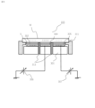
- FIG. 1 is a longitudinal sectional view showing the configuration of a plasma processing apparatus that performs a plasma processing method according to an embodiment of the present invention.
- FIG. 2 is a plan view schematically showing the dispersion plate according to the embodiment.
- FIG. 3 is a vertical cross-sectional view schematically showing the configuration of the sample stage according to the embodiment.
- FIG. 4 is a plan view schematically showing the configuration of the electrostatic attraction film 302 according to the embodiment.
- FIG. 5 is a vertical cross-sectional view schematically showing how a wafer is electrostatically attracted in the embodiment.
- FIG. 6 is a diagram showing a case where a positional shift occurs in the conventional technique.
- FIG. 7 is a time chart showing the wafer processing method according to the embodiment.
- FIG. 8 is a diagram showing an electric circuit from plasma to ground.
- FIG. 9 is a timing chart showing a plasma processing method according to a modification of the embodiment.
- the term "upper surface” refers to the surface shown above in the drawing when a plate-like member or a cross section included in the plate-like member is illustrated. Further, the term “side surface” refers to a plate-like member or a surface in a cross section included in the plate-like member or a thickness of a layer.
- central axis means an axis that passes through the center of a circular surface and extends in a direction perpendicular to the surface.
- FIG. 1 is a longitudinal sectional view showing the configuration of a plasma processing apparatus that performs a plasma processing method according to an embodiment of the present invention.
- the plasma processing apparatus 100 of the embodiment includes a vacuum container 101.
- a processing chamber 104 which is a cylindrical space, is provided inside the vacuum container 101.
- the vacuum container 101 is connected to a vacuum pump 1015 such as a turbo molecular pump via a pressure regulating valve 1016.
- the vacuum pump 1015 exhausts particles in the processing chamber 104 and brings the processing chamber 104 to a predetermined atmospheric pressure.
- the pressure regulating valve 1016 has the function of changing the cross-sectional area of the passage connecting the vacuum pump 1015 and the processing chamber 104, and adjusting the flow rate or speed of exhaust gas.
- the vacuum container 101 includes a discharge chamber 102 on the upstream side of the processing chamber 104.
- the processing chamber 104 is connected via a dispersion plate 106 to the discharge chamber 102 where plasma generation is performed.
- the discharge chamber 102 and the processing chamber 104 are both cylindrical spaces.
- the central axis of the discharge chamber 102 and the central axis of the processing chamber 104 are located at a common axis or close enough to be considered to be a common axis.
- the dispersion plate 106 is provided between the discharge chamber 102 and the processing chamber 104, and partitions the discharge chamber 102 and the processing chamber 104. Specifically, the dispersion plate 106 is arranged in a passage connecting the discharge chamber 102 and the processing chamber 104.
- the passage between the discharge chamber 102 and the processing chamber 104 has a cylindrical shape
- the distribution plate 106 is a disc-shaped plate member having the same diameter as the passage. Details of the distribution plate 106 will be described later.
- a wafer to be processed is placed on the sample stage 103.
- the sample stage 103 is placed at a position facing the dispersion plate 106. Details of the sample stage 103 will be described later.
- the discharge chamber 102 is a space inside a dielectric chamber 107 made of a dielectric (quartz in the embodiment).
- a coil 108 is arranged on the outer peripheral side wall of the dielectric chamber 107 so as to surround the dielectric chamber 107 .
- the coil 108 is electrically connected to a high frequency power source 110 via a matching box 109, and is supplied with high frequency power from the high frequency power source 110.
- the high frequency power power in a frequency band of several tens of MHz such as 13.56 MHz is used.
- a top plate 1012 and a gas distribution plate 10121 are arranged at the upper end of the dielectric chamber 107.
- the top plate 1012 and the gas distribution plate 10121 define the inside and outside of the dielectric chamber 107.
- a passageway extending from a gas source 1013 is coupled to the top plate 1012 . Gas supplied from a gas source 1013 is introduced into the discharge chamber 102 via a gas distribution plate 10121.
- the gas source 1013 has a storage section for each type of gas to be supplied.
- a mass flow controller 1014 provided between the gas source 1013 and the top plate 1012 adjusts the amount of gas introduced into the discharge chamber 102 .
- the processing gas used in the embodiment includes a combustible gas, a combustion-supporting gas, a mixed gas thereof, or a gas diluted with an inert gas.
- the IR lamp unit 105 is arranged so as to surround the passage or the distribution plate 106 that connects the discharge chamber 102 and the processing chamber 104.
- the IR lamp unit 105 heats the sample stage 103, the wafer placed thereon, the inside of the processing chamber 104, etc. by irradiating electromagnetic waves.
- the IR lamp unit 105 is constituted by an IR lamp 1017 that emits electromagnetic waves including an infrared (Infra-Red: IR) band.
- the IR lamp unit 105 includes a reflector 1018 that reflects the IR light emitted from the IR lamp 1017 toward the processing chamber 104, and a reflector plate 1018 that processes the IR light emitted from the IR lamp 1017.
- An IR light transmitting window 1019 is provided that transmits toward the chamber 104 or the dispersion plate 106 .
- wafer processing is performed on a wafer placed on a sample stage 103.
- gas is first introduced into the discharge chamber 102.
- an induced magnetic field is formed at the center of the coil 108.
- ICP inductively coupled plasma
- Processing such as etching is performed using the generated plasma 1011 while heating with the IR lamp unit 105 or adjusting the temperature on the sample stage 103 (described later).
- etching plasma, static elimination plasma, and cleaning plasma are generated depending on the gas and high-frequency power used.
- FIG. 2 is a plan view schematically showing the dispersion plate 106 according to the embodiment. While the dispersion plate 106 shown in FIG. 1 is a cross-sectional view, the dispersion plate 06 shown in FIG. 2 is a view seen from above in FIG.
- the dispersion plate 106 is a circular plate-like member.
- the dispersion plate 106 has a plurality of through holes 201 that allow charged particles to move from the discharge chamber 102 to the processing chamber 104.
- Each of the plurality of through holes 201 is a circular hole.
- three circular holes are arranged from locations beyond a predetermined radius. Three holes are similarly arranged at positions shifted by 15 degrees in the circumferential direction.
- a plurality of through holes 201 are provided in a ring shape on the outer peripheral side of the dispersion plate 106.
- the dispersion plate 106 is made of a dielectric member such as quartz that is transparent. The material is not limited to quartz and can be selected as appropriate.
- neutral particles such as gas radicals contained in the plasma 1011 are uniformly introduced from the discharge chamber 102 into the processing chamber 104. That is, neutral particles such as radicals are introduced into the processing chamber 104 from a ring-shaped portion on the outer circumferential side of the dispersion plate 106, which is disposed at a position facing the wafer placed on the sample stage 103.
- the arrangement of the plurality of through holes 201 as described above is not limited to this.
- the arrangement of the through holes can be appropriately selected so that the distribution of neutral particles such as radicals that reach the surface of the wafer introduced into the processing chamber 104 provides a desired processing result for the film layer to be processed. Note that charged particles such as ions and electrons contained in the plasma 1011 are suppressed from being introduced from the discharge chamber 102 into the processing chamber 104 by the dispersion plate 106 .
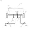
- FIG. 3 is a vertical cross-sectional view schematically showing the configuration of the sample stage 103 according to the embodiment.
- FIG. 4 is a plan view schematically showing the configuration of the electrostatic attraction film 302 according to the embodiment.
- the wafer W is electrostatically attracted and processed in an apparatus including a processing chamber 104 and a sample stage 103 having an electrode capable of electrostatically adsorbing a wafer placed in the processing chamber 104.
- the sample stage 103 shown in FIG. 3 has a cylindrical shape.
- the central axis of the sample stage 103 and the central axis of the processing chamber 104 are located at a common axis or so close that they can be regarded as a common axis.
- the sample stage 103 includes a base material 301 made of a conductor such as metal, an electrostatic adsorption film 302 disposed on the base material 301, and a structure surrounding the side surfaces of the base material 301 and the electrostatic adsorption film 302.
- a susceptor ring 311 is provided.
- the wafer placed on the sample stage 103 will be placed on the electrostatic adsorption film 302.
- the electrostatic adsorption film 302 comes into contact with the wafer and grips the wafer by electrostatic adsorption.
- the electrostatic adsorption film 302 includes a sheet S made of polyimide resin.
- a sheet S made of polyimide resin is provided on the surface of the electrostatic adsorption film 302.
- the susceptor ring 311 is made of a dielectric material and has a function of protecting the base material 301 from the plasma 1011.
- the susceptor ring 311 of the embodiment has a shape that surrounds the side wall of the electrostatic adsorption film 302 on the upper part of the base material 301 and covers from the side wall of the base material 301 to the lower part of the base material 301.
- a refrigerant flow path 303 is arranged inside the base material 301. Refrigerant is supplied from the chiller 312 to the refrigerant flow path 303 , and the supplied refrigerant circulates through the refrigerant flow path 303 .
- the chiller 312 is arranged in a space below the floor of a building such as a clean room in which the plasma processing apparatus 100 is arranged, and is connected to the coolant flow path 303.
- the wafer placed on the sample stage 103 is adjusted to a desired temperature suitable for wafer processing by exchanging heat with the coolant flowing through the coolant flow path 303 via the electrostatic adsorption film 302 and the base material 301.
- the shape of the coolant flow path 303 may be, for example, arranged concentrically with respect to a central axis that is perpendicular to the surface direction of the base material 301, or arranged spirally. Good too.
- a plurality of grooves 308 are formed on the upper surface of the electrostatic attraction film 302.
- the heat transfer gas source 310 supplies a gas having heat transfer properties such as He gas through a path having a valve 309 that opens and closes.
- the gas supplied from the heat transfer gas source 310 diffuses along the groove 308 and reaches the back surface of the wafer W.
- the He gas filling the groove 308 promotes heat transfer between the coolant flowing through the coolant channel 303 and the wafer W, and the temperature of the wafer W is efficiently controlled.
- the surface of the electrostatic adsorption film 302 is constituted by a sheet S made of polyimide resin.
- the polyimide resin sheet S is a film made of a resin material containing polyimide.
- Polyimide resins are generally known to have a low coefficient of friction, wear resistance, and excellent insulation properties.
- the polyimide resin sheet S prevents scratches on the back side of the wafer due to expansion or contraction of the wafer, even if the temperature changes due to heating or cooling while the wafer is electrostatically attracted. There is a function to Note that the material of the sheet S is not limited to this, and can be selected as appropriate.
- FIG. 4 shows a cross-sectional structure when the electrostatic adsorption film 302 is cut in the plane direction.
- a plurality of film-like electrodes 304 and 305 are arranged inside the electrostatic adsorption film 302.
- DC power is supplied to the electrode 304 from a DC power supply 306, and DC power is supplied to the electrode 305 from a DC power supply 307.
- the electrodes 304 and 30 each have a plurality of arc-shaped arm portions arranged concentrically around the central axis in the plane direction of the sample stage 103, so that the arm of one electrode is connected to the other electrode. It has a so-called comb-like arrangement, sandwiched between the arms of the body. Note that the shapes of the electrodes 304 and 305 are not limited to this. Any material may be used as long as it is evenly distributed within the electrostatic adsorption film 302.
- FIG. 5 is a vertical cross-sectional view schematically showing how a wafer is electrostatically attracted in the embodiment.
- the sample stage 103 shown in FIG. 5 is the same as the sample stage 103 shown in FIG. 3.
- the constituent elements shown in FIG. 3 are omitted, and constituent elements not shown in FIG. 3 are also shown.
- the sizes of the configurations are shown changed to make it easier to understand.
- a ⁇ voltage is applied to the electrode 304 from a DC power source 306, and a + voltage is applied to the electrode 305 from a DC power source 307.
- a dipole electrode is formed between the electrodes 304 and 305.
- the + ions in the wafer W approach the - voltage electrode 304, and the - ions approach the + voltage electrode 305, respectively.
- Electrostatic forces are generated between the + ions in the wafer W and the electrode 304 and between the - ions in the wafer W and the electrode 305, and the wafer W is attracted to the sample stage 103.
- a voltage of -1500V is applied to the electrode 304 from a DC power supply 306, and a voltage of 1500V is applied to the other electrode 305 from a DC power supply 307.
- the voltage when a voltage of 1500V is applied to the electrode 304 by the DC power supply 306, the voltage may be adjusted so that a voltage of -1500V is applied to the electrode 305 from the DC power supply 307.
- the voltage from the DC power supplies 306 and 307 is ⁇ 1500V, and is adjusted so that voltages of the same magnitude and different polarity are applied from one DC power supply and the other DC power supply, but the present invention is not limited to this. . If the wafer W can be attracted onto the electrostatic adsorption film 302 and the occurrence and amount of positional deviation can be kept within the permissible range when holding or attaching or removing the wafer W, a voltage exceeding ⁇ 1500 V or less may be used. Even if it is used, the absolute value of the voltage applied to each electrode does not have to be the same. Further, the electrodes 304 and 305 may be given the same polarity.
- the plasma processing apparatus 100 extends from the inside of the sample stage 103 toward the top surface of the sample stage 103.
- a plurality of (for example, three) push-up pins 313 are provided. After the electrostatic adsorption of the wafer W is released, the push-up pins 313 housed inside the sample stage 103 move upward and push up the wafer W, thereby making it possible to remove the wafer W from the sample stage 103. can.
- the detached wafer W is held by a transfer mechanism such as a robot arm and carried out from the processing chamber 104.
- FIG. 6 is a diagram showing a case where a positional shift occurs in the conventional technique.
- the first phenomenon is caused by charged particles generated during processing.
- the electrostatic adsorption film 302 may be damaged by collisions with charged particles such as ions, or may have reaction products attached thereto.
- power is generally not supplied to the electrodes 304 and 305 in the electrostatic attraction film 302 during waferless plasma processing.
- charged particles such as ions adhere to the electrostatic adsorption film 302 they will be removed as shown in FIG. , remains on the surface of the electrostatic adsorption film 302 as a negative charge.
- the potential of the surface of the electrostatic adsorption film 302 was detected before and during waferless plasma processing using the plasma processing apparatus 100, and as a result, it was found that the potential varied before and after the processing. There was found. From this, as described above, it is assumed that charges exist in the electrostatic adsorption film 302 in the process of processing using waferless plasma.
- the second phenomenon is caused by the dispersion plate 106.
- the dispersion plate 106 can prevent charged particles such as ions from moving to the processing chamber 104 at locations where the through holes 201 are not arranged, some of the charged particles may pass through the locations where the through holes 201 are arranged and enter the discharge chamber. 102 and flows into the processing chamber 104 . Due to the nature of the distribution of the through holes, a relatively large amount of the charged particles that have flowed in adhere to the outer peripheral portion of the surface of the electrostatic adsorption film 302.
- the wafer W is electrostatically attracted to the sample stage 103 with charged particles attached to it in this way, there is a possibility that partial adsorption, in which a large electrostatic adsorption force acts locally on a portion of the back surface of the wafer W, may occur.
- the wafer W is partially attracted, even if the static elimination step after the plasma treatment shown in the prior art is performed, the charge in the electrostatic adsorption film 302 is not sufficiently reduced and the electrostatic force remains. Therefore, residual adsorption force acts on the wafer W, making it difficult to detach the wafer W from the sample stage 103, and there is a risk that a large force will be applied during detachment, causing damage or misalignment of the wafer W. be.
- the third phenomenon is caused by the sheet S made of polyimide resin.
- the wafer mounting surface of the electrostatic adsorption film 302 is constituted by a sheet S made of polyimide resin. It is generally known that highly insulating substances such as polyimide resin have properties that make it difficult to conduct electricity and that charged particles tend to remain. Therefore, the electric charge cannot be sufficiently removed only by performing the static elimination step shown in the prior art.
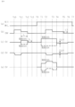
- FIG. 7 is a time chart showing the wafer processing method according to the embodiment.
- FIG. 7A shows the presence or absence of the wafer W on the sample stage 103.
- FIG. 7B shows the output (power) of the high-frequency power source 110 that supplies high-frequency power for forming the plasma 1011 to the coil 108.
- FIG. 7(c) shows the potentials of electrodes 304 and 305.
- FIG. 7(d) shows the potential on the surface of the wafer W or the electrostatic attraction film 302.
- FIG. 7E shows the potential difference between the electrode 304 and the wafer W or the potential difference between the electrode 305 and the wafer W.
- a wafer-less static elimination process is performed to remove charged particles remaining on the electrostatic adsorption film 302.
- the wafer-less static elimination process is performed in a so-called wafer-less state where there is no member covering the upper surface of the sample stage 103 on which the wafer is placed. As shown in FIG. 7A, the waferless state continues from time Tp0 to time Tp2.
- FIG. 7E showing the potential difference, no potential is shown in the static elimination process from Tp0 to Tp2.
- the plasma 1011 is formed in the discharge chamber 102, charged particles such as generated ions enter the processing chamber 104 and adhere to the surface of the electrostatic adsorption film 302 of the sample stage 103. Therefore, the potential from time Tp0 to time Tp2 in FIG. 7(d) indicates the potential of the electrostatic attraction film 302.
- a wafer-less charge removal process is performed in which the charges accumulated on the sample stage 103 are removed without placing a wafer on the sample stage 103.
- first static elimination gas for generating static elimination plasma
- a gas such as SF 6 that is reactive with deposits or an inert gas such as Ar is used. It will be done.
- a static eliminating gas a gas that causes less damage to the polyimide resin, which is a material forming the electrostatic adsorption film 302, is selected. Note that such gases include gases that have not only a static eliminating effect but also a cleaning effect of removing reaction products and the like attached to the processing chamber 104.
- a plasma generation step is performed in which plasma is generated using the first static elimination gas.
- plasma is generated from the first static elimination gas in the discharge chamber 102 using high frequency power.
- high frequency power hereinafter also referred to as "first high frequency power”
- first high frequency power is supplied from the high frequency power supply 110 to the coil 108.
- the first static elimination gas introduced in advance exists in the discharge chamber 102.
- a power supply step is performed in which first power is supplied to the electrodes 304 and 305 of the sample stage 103.
- first power is supplied to the electrodes 304 and 305 of the sample stage 103.
- 100V is applied from the DC power supply 306 to the electrode 304
- -100V is applied to the electrode 305 from the DC power supply 307.
- FIG. 8 is a diagram showing an electric circuit from plasma to ground.
- the dashed line indicates the flow of charge.
- Charged particles generated in plasma 1011 reach the ground connected to DC power source 306 or 307 via electrostatic adsorption film 302, electrode 304 or 305, push-up pin 313, and base material 301. Further, the charges generated in the plasma 1011 directly adhere to the push-up pin 313 and reach the ground connected to the base material 301 and the DC power source 306 or 307. It is assumed that the charged particles attached to the electrostatic adsorption film 302 reach the ground in this way.
- time Tp1 refers to the time when the charged particles remaining in the processing chamber 104 disappear. Therefore, time Tp1 may be extended to time Tp02, which is delayed by a period t1 until the afterglow discharge of plasma 1011 disappears.
- a wafer processing process is performed in which the wafer W placed on the sample stage 103 is electrostatically attracted and the wafer W is processed.
- the wafer processing process includes a wafer etching process and a static elimination process while the wafer is being placed.
- the wafer processing step includes a mounting step, an electrostatic adsorption step, and a plasma etching step, and the static elimination step during wafer mounting includes a static elimination plasma generation step and a potential difference reduction step.
- a mounting step is performed in which the wafer W is mounted on the sample stage 103.
- the wafer W is carried into the processing chamber 104 by a transfer mechanism such as a robot arm and placed on the sample stage 103.
- an electrostatic adsorption step is performed in which second power is supplied to the electrodes 304 and 305 of the sample stage 103 to electrostatically adsorb the wafer W.
- second power is supplied to the electrodes 304 and 305 of the sample stage 103 to electrostatically adsorb the wafer W.
- a voltage is applied to the electrodes 304 and 305, and the wafer W is electrostatically attracted onto the electrostatic adsorption film 302.
- the voltage applied to the electrode 304 and the voltage applied to the electrode 305 are adjusted to have different polarities and equal absolute values. As described above, for example, -1500V is applied to electrode 304 and 1500V is applied to electrode 305.
- a plasma etching process is performed in which a processing gas is supplied to the discharge chamber 102 and plasma is generated from the processing gas using second high-frequency power.
- the second high frequency power is supplied from the high frequency power supply 110 to the coil 108, as shown in FIG. 7(b).
- etching plasma 1011 is generated from the processing gas introduced into the discharge chamber 102.
- Reactive particles such as radicals that have passed through the dispersion plate 106 react with the film layer to be processed on the surface of the wafer W, and plasma etching progresses.
- a static electricity removal process is performed while the wafer is being placed.
- the static elimination process during wafer placement is a process of supplying the second static elimination gas to the discharge chamber 102 and generating plasma from the second static elimination gas using the third high-frequency power.
- the high frequency power supplied from the high frequency power supply 110 to the coil 108 is changed to a high frequency power (hereinafter referred to as "third high frequency power") different from the second high frequency power during the etching process. ).
- the gas introduced into the discharge chamber 102 is switched from the processing gas to a static elimination gas (hereinafter referred to as "second static elimination gas") that has less influence on the wafer W, such as an inert gas.
- second static elimination gas a static elimination plasma generation step is performed in which the static elimination plasma 1011 is generated from the second static elimination gas using the third high-frequency power.
- a potential difference reduction step is performed in which a second power is applied so that the electrodes 304 and 305 of the sample stage 103 have a potential equal to the potential of the wafer W.
- the voltage applied to the electrodes 304 and 305 as the supplied second power is - ⁇ V, which is equal to the potential of the wafer W.
- the potential of the wafer W can be determined in advance.
- the potential of the wafer W may be measured after the plasma 1011 for static elimination is generated after time T3.
- Time T6 when a predetermined time t2 has elapsed from time T5, represents the time when the charged particles remaining in the processing chamber 104 disappear.
- the predetermined time t2 may be a time until the afterglow discharge of the static elimination plasma 1011 disappears.
- the resistance value of the electrostatic adsorption film 302 is sufficiently large, the potential of the wafer W is changed by the plasma treatment for static elimination starting from time T3, as shown in FIG. 7(d).
- the middle value - ⁇ V is maintained as is.
- the potentials of electrodes 304 and 305 are also unchanged from time T4.
- the potential difference between the wafer W and the electrode 304 and the potential difference between the wafer W and the electrode 305 remain at 0V from time T4 as shown in FIG. There is no electrostatic adsorption force between the two.
- the voltage applied to the electrodes 304 and 305 is set to 0V.
- the potential of the electrodes 304 and 305 changes, and the potential of the wafer W also changes following the change in the potential of the electrodes 304 and 305, and becomes approximately 0V.
- the potential difference between the wafer W and the electrode 304 and the potential difference between the wafer W and the electrode 305 are maintained at approximately 0V even after T6. That is, the potentials of the electrodes 304 and 305 can be set to 0V in a state where the electrostatic attraction force between the wafer W and the electrode 304 and the electrostatic attraction force between the wafer W and the electrode 305 are eliminated.
- the wafer W is removed from the sample stage 103 by the push-up pins 313 and carried out to the outside of the processing chamber 104.
- first power, the second power, the first high frequency power, the second high frequency power, and the third high frequency power can be appropriately set according to the manufacturing conditions and the purpose of the process. It is also possible to use the same type of gas for the first static elimination gas and the second static elimination gas, or it is also possible to use different types of gas. Furthermore, the size of the time in the time chart can also be set as appropriate.
- FIG. 9 is a timing chart showing a plasma processing method according to a modification of the embodiment.
- FIG. 9A shows the presence or absence of the wafer W on the sample stage 103.
- FIG. 9B shows the output (power) of the high frequency power supply 110 that supplies high frequency power for forming the plasma 1011 to the coil 108.
- FIG. 9(c) shows the potentials of the electrostatic adsorption electrodes 304 and 305.
- FIG. 9(d) shows the potential on the surface of the wafer W or the electrostatic attraction film 302.
- FIG. 9E shows the potential difference between the electrode 304 and the wafer W and the potential difference between the electrode 305 and the wafer W.
- the modified example differs from the embodiment in that a static elimination process is performed after cleaning.
- differences appear between FIG. 9(b), FIG. 9(c), and FIG. 9(d).
- the same reference numerals are given to the same or equivalent components as in the above-described embodiment, and the description thereof will be simplified or omitted.
- a step of cleaning the discharge chamber 102 and the processing chamber 104 is performed without a wafer.
- high frequency power hereinafter also referred to as "fourth high frequency power”
- cleaning gas is introduced into the discharge chamber 102.
- a gas that causes little damage to the polyimide resin such as SF 6 gas and Ar gas, is selected. In this way, plasma 1011 for performing cleaning is generated.
- a post-cleaning static elimination process for reducing the charge on the electrostatic adsorption film 302 will be described.
- plasma 1011 for static elimination is generated.
- the high frequency power supplied from the high frequency power supply 110 to the coil 108 is a high frequency power (hereinafter also referred to as "fifth high frequency power") that is different from the fourth high frequency power during cleaning.
- Change to The fifth high frequency power is, for example, 1000W.
- the gas introduced into the discharge chamber 102 is switched from a cleaning gas to a static elimination gas (hereinafter also referred to as "third static elimination gas") such as an inert gas such as Ar gas.
- a static elimination plasma generation procedure is performed in which the static elimination plasma 1011 is generated from the third static elimination gas using the fifth high-frequency power.
- a residual charge removal step is performed in which third power is supplied to the electrodes 304 and 305 of the sample stage 103.
- the third power supplied for example, 100V is applied from the DC power supply 306 to the electrode 304, and -100V is applied to the electrode 305 from the DC power supply 307. These voltages are lower than the voltages applied when electrostatically adsorbing the wafer W.
- the time when the high frequency power is changed to generate the plasma for static elimination and the time when the voltage is applied to the electrodes 304 and 305 are not limited to the same time. As shown in FIG. 9B, application of voltage to the electrodes 304 and 305 may be started within the time ta between time Tc1 and time Tc2 when plasma 1011 for static elimination is formed. Furthermore, after applying the voltage to the electrodes 304 and 305, the high frequency power may be changed to generate the plasma 1011 for static elimination. In any case, it is necessary that the period during which the static elimination plasma 1011 is generated and the period during which the voltage is applied to the electrodes 304 and 305 at least overlap, and in a modified example, the periods overlap by 1 second or more.
- the power supply from the high frequency power supply 110 to the coil 108 is stopped as shown in FIG. 9(b). Further, as shown in FIG. 9(c), the voltage applied to the electrodes 304 and 305 is set to 0V. Similar to the embodiment, the period from time Tc1 to time Tc2 is a period in which charged particles remaining in the processing chamber 104 are sufficiently removed, and is a period in which the afterglow discharge of the static elimination plasma 1011 disappears. It may be extended by tb.
- the post-cleaning static elimination process ends. Thereafter, the wafer W is transferred to the processing chamber 104, and a predetermined wafer processing process is performed.
- the wafer processing process is the same as in the embodiment.
- the fourth high-frequency power, the fifth high-frequency power, the third static elimination gas, and the third power can be appropriately set according to the manufacturing conditions and the purpose of the process, as in the embodiment. Furthermore, the size of the time in the time chart can also be set as appropriate.
- the inventors conducted experiments and studied the relationship between the voltage applied to the electrodes 304 and 305, the voltage application time, and the static elimination effect in the static elimination step of reducing the charge on the electrostatic adsorption film 302.
- the power of the high-frequency power source 110 set to 1000 W
- the voltage applied to the electrodes 304 and 305 set to a value in the range of ⁇ 100 V to ⁇ 500 V
- the electrostatic adsorption film 302 was sufficiently strong. It was confirmed that the static electricity was removed and the positional shift when the wafer W was attached to and detached from the sample stage 103 was suppressed.
- the polarities of the voltages applied to the electrodes 304 and 305 are different, but even if the polarities are the same, the same static elimination effect can be achieved.
- the output of the high frequency power source 110 may be changed, or the electrostatic attraction film 302 made of another highly insulating material may be used. Further, in accordance with these changes, the value of the voltage applied to the electrodes 304 and 305 and the time of the process can be appropriately changed.
- inductively coupled plasma 1011 is formed, and the present invention is applicable regardless of the plasma generation method.
- the present invention is applicable to a helicon wave plasma processing apparatus, an ECR plasma processing apparatus using microwaves, a capacitively coupled plasma processing apparatus, and the like.
- Plasma processing apparatus 101... Vacuum vessel 102... Discharge chamber 103... Sample stand 104... Processing chamber 105... IR lamp unit 106... Dispersion plate 107... Dielectric material Chamber 108... Coil 109... Matching box 110... High frequency power supply 201... Through holes 301, 301a... Base material 302, 302a... Electrostatic adsorption film 303... Refrigerant circuit 304, 305... ... Electrodes 306, 307 ... DC power supply 308 ... Groove 309 ... Valve 310 ... Heat transfer gas source 311 ... Susceptor ring 312 ... Chiller 313 ... Push-up pin 1011 ... Plasma 1012...Top plate 10121...Gas distribution plate 1014...Mass flow controller 1015...Vacuum pump 1016...Pressure regulating valve 1017...IR lamp 1018...Reflector plate 1019...IR light transmission window
Landscapes
- Physics & Mathematics (AREA)
- Engineering & Computer Science (AREA)
- Plasma & Fusion (AREA)
- Chemical & Material Sciences (AREA)
- Analytical Chemistry (AREA)
- Container, Conveyance, Adherence, Positioning, Of Wafer (AREA)
- Drying Of Semiconductors (AREA)
Priority Applications (6)
| Application Number | Priority Date | Filing Date | Title |
|---|---|---|---|
| US18/280,569 US20250038033A1 (en) | 2022-08-03 | 2022-08-03 | Semiconductor wafer processing method |
| CN202280019021.0A CN117836912A (zh) | 2022-08-03 | 2022-08-03 | 晶片处理方法 |
| PCT/JP2022/029761 WO2024029000A1 (ja) | 2022-08-03 | 2022-08-03 | ウエハ処理方法 |
| KR1020237030055A KR102859137B1 (ko) | 2022-08-03 | 2022-08-03 | 웨이퍼 처리 방법 |
| JP2023553340A JP7612889B2 (ja) | 2022-08-03 | 2022-08-03 | ウエハ処理方法 |
| TW112128974A TWI875108B (zh) | 2022-08-03 | 2023-08-02 | 晶圓處理方法 |
Applications Claiming Priority (1)
| Application Number | Priority Date | Filing Date | Title |
|---|---|---|---|
| PCT/JP2022/029761 WO2024029000A1 (ja) | 2022-08-03 | 2022-08-03 | ウエハ処理方法 |
Publications (1)
| Publication Number | Publication Date |
|---|---|
| WO2024029000A1 true WO2024029000A1 (ja) | 2024-02-08 |
Family
ID=89848757
Family Applications (1)
| Application Number | Title | Priority Date | Filing Date |
|---|---|---|---|
| PCT/JP2022/029761 Ceased WO2024029000A1 (ja) | 2022-08-03 | 2022-08-03 | ウエハ処理方法 |
Country Status (6)
| Country | Link |
|---|---|
| US (1) | US20250038033A1 (https=) |
| JP (1) | JP7612889B2 (https=) |
| KR (1) | KR102859137B1 (https=) |
| CN (1) | CN117836912A (https=) |
| TW (1) | TWI875108B (https=) |
| WO (1) | WO2024029000A1 (https=) |
Citations (3)
| Publication number | Priority date | Publication date | Assignee | Title |
|---|---|---|---|---|
| JP2002222799A (ja) * | 2001-01-25 | 2002-08-09 | Tokyo Electron Ltd | プラズマ処理装置およびそのクリーニング方法および静電チャックの除電方法 |
| JP2017216346A (ja) * | 2016-05-31 | 2017-12-07 | 東京エレクトロン株式会社 | プラズマ処理装置、プラズマ処理方法及び記憶媒体 |
| JP2022024265A (ja) * | 2020-07-13 | 2022-02-09 | 東京エレクトロン株式会社 | 基板離脱方法及びプラズマ処理装置 |
Family Cites Families (5)
| Publication number | Priority date | Publication date | Assignee | Title |
|---|---|---|---|---|
| JP2002217166A (ja) | 2001-01-19 | 2002-08-02 | Toshiba Corp | ガス処理装置のクリーニング方法 |
| JP6708358B2 (ja) * | 2016-08-03 | 2020-06-10 | 株式会社日立ハイテク | プラズマ処理装置及び試料の離脱方法 |
| JP7462383B2 (ja) | 2019-04-15 | 2024-04-05 | 東京エレクトロン株式会社 | クリーニング方法及びプラズマ処理装置 |
| JP7340953B2 (ja) * | 2019-04-26 | 2023-09-08 | 東京エレクトロン株式会社 | 除電方法、基板処理方法及び基板処理装置 |
| US20250218745A1 (en) * | 2022-05-20 | 2025-07-03 | Nextin, Inc. | Static electrcity control device for semiconductor processing system |
-
2022
- 2022-08-03 KR KR1020237030055A patent/KR102859137B1/ko active Active
- 2022-08-03 US US18/280,569 patent/US20250038033A1/en active Pending
- 2022-08-03 WO PCT/JP2022/029761 patent/WO2024029000A1/ja not_active Ceased
- 2022-08-03 CN CN202280019021.0A patent/CN117836912A/zh active Pending
- 2022-08-03 JP JP2023553340A patent/JP7612889B2/ja active Active
-
2023
- 2023-08-02 TW TW112128974A patent/TWI875108B/zh active
Patent Citations (3)
| Publication number | Priority date | Publication date | Assignee | Title |
|---|---|---|---|---|
| JP2002222799A (ja) * | 2001-01-25 | 2002-08-09 | Tokyo Electron Ltd | プラズマ処理装置およびそのクリーニング方法および静電チャックの除電方法 |
| JP2017216346A (ja) * | 2016-05-31 | 2017-12-07 | 東京エレクトロン株式会社 | プラズマ処理装置、プラズマ処理方法及び記憶媒体 |
| JP2022024265A (ja) * | 2020-07-13 | 2022-02-09 | 東京エレクトロン株式会社 | 基板離脱方法及びプラズマ処理装置 |
Also Published As
| Publication number | Publication date |
|---|---|
| TW202407802A (zh) | 2024-02-16 |
| KR102859137B1 (ko) | 2025-09-12 |
| JP7612889B2 (ja) | 2025-01-14 |
| US20250038033A1 (en) | 2025-01-30 |
| CN117836912A (zh) | 2024-04-05 |
| KR20240019752A (ko) | 2024-02-14 |
| JPWO2024029000A1 (https=) | 2024-02-08 |
| TWI875108B (zh) | 2025-03-01 |
Similar Documents
| Publication | Publication Date | Title |
|---|---|---|
| US6057244A (en) | Method for improved sputter etch processing | |
| CN111668085B (zh) | 等离子体处理装置 | |
| JP5390846B2 (ja) | プラズマエッチング装置及びプラズマクリーニング方法 | |
| TWI553717B (zh) | A focusing ring and a substrate processing device provided with the focusing ring | |
| TWI689033B (zh) | 於載置台吸附被吸附物之方法及處理裝置 | |
| JP5976377B2 (ja) | 被処理基体に対する微粒子付着の制御方法、及び、処理装置 | |
| JP6552346B2 (ja) | 基板処理装置 | |
| JP4322484B2 (ja) | プラズマ処理方法及びプラズマ処理装置 | |
| JP4642809B2 (ja) | プラズマ処理方法及びプラズマ処理装置 | |
| JP5317509B2 (ja) | プラズマ処理装置および方法 | |
| TWI756424B (zh) | 電漿處理裝置之洗淨方法 | |
| CN113936986B (zh) | 基板脱离方法和等离子体处理装置 | |
| CN100570818C (zh) | 等离子体处理装置 | |
| US20140308817A1 (en) | Etching method | |
| KR20010079817A (ko) | 플라스마 처리 장치 | |
| JP6298293B2 (ja) | 基板処理装置、シャッタ機構およびプラズマ処理装置 | |
| TWI698928B (zh) | 電漿處理方法 | |
| WO2024029000A1 (ja) | ウエハ処理方法 | |
| JP3157551B2 (ja) | 被処理体用載置装置及びそれを用いた処理装置 | |
| JP4832222B2 (ja) | プラズマ処理装置 | |
| TWI919449B (zh) | 基於電漿的處理系統及減輕電漿處理腔室的操作的期間的蓋加熱方法 | |
| US20250316520A1 (en) | Bipolar esc to prevent substrate backside discharging | |
| JPWO2024029000A5 (https=) | ||
| JP2000124139A (ja) | プラズマ処理装置 |
Legal Events
| Date | Code | Title | Description |
|---|---|---|---|
| ENP | Entry into the national phase |
Ref document number: 2023553340 Country of ref document: JP Kind code of ref document: A |
|
| WWE | Wipo information: entry into national phase |
Ref document number: 202280019021.0 Country of ref document: CN |
|
| WWE | Wipo information: entry into national phase |
Ref document number: 18280569 Country of ref document: US |
|
| 121 | Ep: the epo has been informed by wipo that ep was designated in this application |
Ref document number: 22953989 Country of ref document: EP Kind code of ref document: A1 |
|
| NENP | Non-entry into the national phase |
Ref country code: DE |
|
| 122 | Ep: pct application non-entry in european phase |
Ref document number: 22953989 Country of ref document: EP Kind code of ref document: A1 |