WO2024029000A1 - Method for wafer treatment - Google Patents
Method for wafer treatment Download PDFInfo
- Publication number
- WO2024029000A1 WO2024029000A1 PCT/JP2022/029761 JP2022029761W WO2024029000A1 WO 2024029000 A1 WO2024029000 A1 WO 2024029000A1 JP 2022029761 W JP2022029761 W JP 2022029761W WO 2024029000 A1 WO2024029000 A1 WO 2024029000A1
- Authority
- WO
- WIPO (PCT)
- Prior art keywords
- wafer
- plasma
- static elimination
- sample stage
- gas
- Prior art date
Links
- 238000000034 method Methods 0.000 title claims abstract description 40
- 238000011282 treatment Methods 0.000 title abstract description 7
- 238000012545 processing Methods 0.000 claims description 98
- 230000003068 static effect Effects 0.000 claims description 79
- 239000007789 gas Substances 0.000 claims description 75
- 238000003379 elimination reaction Methods 0.000 claims description 72
- 230000008030 elimination Effects 0.000 claims description 53
- 230000008569 process Effects 0.000 claims description 28
- 238000003672 processing method Methods 0.000 claims description 16
- 238000005530 etching Methods 0.000 claims description 12
- 230000005611 electricity Effects 0.000 claims description 5
- 239000011261 inert gas Substances 0.000 claims description 5
- 238000001020 plasma etching Methods 0.000 claims description 5
- 238000001179 sorption measurement Methods 0.000 description 59
- 239000002245 particle Substances 0.000 description 37
- 238000004140 cleaning Methods 0.000 description 28
- 239000006185 dispersion Substances 0.000 description 23
- 239000000463 material Substances 0.000 description 19
- 229920001721 polyimide Polymers 0.000 description 13
- 239000009719 polyimide resin Substances 0.000 description 12
- 150000002500 ions Chemical class 0.000 description 11
- 238000009826 distribution Methods 0.000 description 10
- 230000000694 effects Effects 0.000 description 7
- 238000012546 transfer Methods 0.000 description 7
- 239000007795 chemical reaction product Substances 0.000 description 6
- 239000002826 coolant Substances 0.000 description 6
- 239000003507 refrigerant Substances 0.000 description 6
- 238000010586 diagram Methods 0.000 description 4
- 230000004048 modification Effects 0.000 description 4
- 238000012986 modification Methods 0.000 description 4
- 238000009832 plasma treatment Methods 0.000 description 4
- 238000002474 experimental method Methods 0.000 description 3
- 238000004519 manufacturing process Methods 0.000 description 3
- 230000007935 neutral effect Effects 0.000 description 3
- 230000002093 peripheral effect Effects 0.000 description 3
- 239000010453 quartz Substances 0.000 description 3
- 230000001105 regulatory effect Effects 0.000 description 3
- 239000004065 semiconductor Substances 0.000 description 3
- VYPSYNLAJGMNEJ-UHFFFAOYSA-N silicon dioxide Inorganic materials O=[Si]=O VYPSYNLAJGMNEJ-UHFFFAOYSA-N 0.000 description 3
- 230000009471 action Effects 0.000 description 2
- 238000013459 approach Methods 0.000 description 2
- 230000008859 change Effects 0.000 description 2
- 239000000470 constituent Substances 0.000 description 2
- 238000007796 conventional method Methods 0.000 description 2
- 239000003989 dielectric material Substances 0.000 description 2
- 238000006073 displacement reaction Methods 0.000 description 2
- 238000010438 heat treatment Methods 0.000 description 2
- 238000009616 inductively coupled plasma Methods 0.000 description 2
- 230000007246 mechanism Effects 0.000 description 2
- 230000009467 reduction Effects 0.000 description 2
- 238000003860 storage Methods 0.000 description 2
- BSYNRYMUTXBXSQ-UHFFFAOYSA-N Aspirin Chemical compound CC(=O)OC1=CC=CC=C1C(O)=O BSYNRYMUTXBXSQ-UHFFFAOYSA-N 0.000 description 1
- 239000004642 Polyimide Substances 0.000 description 1
- 238000009825 accumulation Methods 0.000 description 1
- 230000005540 biological transmission Effects 0.000 description 1
- 239000004020 conductor Substances 0.000 description 1
- 230000008602 contraction Effects 0.000 description 1
- 238000001816 cooling Methods 0.000 description 1
- 230000007423 decrease Effects 0.000 description 1
- 230000003111 delayed effect Effects 0.000 description 1
- 238000011161 development Methods 0.000 description 1
- 239000011810 insulating material Substances 0.000 description 1
- 238000009413 insulation Methods 0.000 description 1
- 230000001678 irradiating effect Effects 0.000 description 1
- 239000002184 metal Substances 0.000 description 1
- 238000005192 partition Methods 0.000 description 1
- 230000000737 periodic effect Effects 0.000 description 1
- 239000011347 resin Substances 0.000 description 1
- 229920005989 resin Polymers 0.000 description 1
- 239000000126 substance Substances 0.000 description 1
- 230000008685 targeting Effects 0.000 description 1
- 238000011144 upstream manufacturing Methods 0.000 description 1
Images


Classifications
-
- H—ELECTRICITY
- H01—ELECTRIC ELEMENTS
- H01J—ELECTRIC DISCHARGE TUBES OR DISCHARGE LAMPS
- H01J37/00—Discharge tubes with provision for introducing objects or material to be exposed to the discharge, e.g. for the purpose of examination or processing thereof
- H01J37/32—Gas-filled discharge tubes
- H01J37/32009—Arrangements for generation of plasma specially adapted for examination or treatment of objects, e.g. plasma sources
- H01J37/32082—Radio frequency generated discharge
- H01J37/321—Radio frequency generated discharge the radio frequency energy being inductively coupled to the plasma
-
- H—ELECTRICITY
- H01—ELECTRIC ELEMENTS
- H01J—ELECTRIC DISCHARGE TUBES OR DISCHARGE LAMPS
- H01J37/00—Discharge tubes with provision for introducing objects or material to be exposed to the discharge, e.g. for the purpose of examination or processing thereof
- H01J37/32—Gas-filled discharge tubes
- H01J37/32009—Arrangements for generation of plasma specially adapted for examination or treatment of objects, e.g. plasma sources
- H01J37/32082—Radio frequency generated discharge
- H01J37/32174—Circuits specially adapted for controlling the RF discharge
-
- H—ELECTRICITY
- H01—ELECTRIC ELEMENTS
- H01J—ELECTRIC DISCHARGE TUBES OR DISCHARGE LAMPS
- H01J37/00—Discharge tubes with provision for introducing objects or material to be exposed to the discharge, e.g. for the purpose of examination or processing thereof
- H01J37/32—Gas-filled discharge tubes
- H01J37/32431—Constructional details of the reactor
- H01J37/32697—Electrostatic control
-
- H—ELECTRICITY
- H01—ELECTRIC ELEMENTS
- H01L—SEMICONDUCTOR DEVICES NOT COVERED BY CLASS H10
- H01L21/00—Processes or apparatus adapted for the manufacture or treatment of semiconductor or solid state devices or of parts thereof
- H01L21/02—Manufacture or treatment of semiconductor devices or of parts thereof
- H01L21/04—Manufacture or treatment of semiconductor devices or of parts thereof the devices having at least one potential-jump barrier or surface barrier, e.g. PN junction, depletion layer or carrier concentration layer
- H01L21/18—Manufacture or treatment of semiconductor devices or of parts thereof the devices having at least one potential-jump barrier or surface barrier, e.g. PN junction, depletion layer or carrier concentration layer the devices having semiconductor bodies comprising elements of Group IV of the Periodic System or AIIIBV compounds with or without impurities, e.g. doping materials
- H01L21/30—Treatment of semiconductor bodies using processes or apparatus not provided for in groups H01L21/20 - H01L21/26
- H01L21/302—Treatment of semiconductor bodies using processes or apparatus not provided for in groups H01L21/20 - H01L21/26 to change their surface-physical characteristics or shape, e.g. etching, polishing, cutting
- H01L21/306—Chemical or electrical treatment, e.g. electrolytic etching
- H01L21/3065—Plasma etching; Reactive-ion etching
-
- H—ELECTRICITY
- H01—ELECTRIC ELEMENTS
- H01L—SEMICONDUCTOR DEVICES NOT COVERED BY CLASS H10
- H01L21/00—Processes or apparatus adapted for the manufacture or treatment of semiconductor or solid state devices or of parts thereof
- H01L21/67—Apparatus specially adapted for handling semiconductor or electric solid state devices during manufacture or treatment thereof; Apparatus specially adapted for handling wafers during manufacture or treatment of semiconductor or electric solid state devices or components ; Apparatus not specifically provided for elsewhere
- H01L21/67005—Apparatus not specifically provided for elsewhere
- H01L21/67011—Apparatus for manufacture or treatment
- H01L21/67017—Apparatus for fluid treatment
- H01L21/67063—Apparatus for fluid treatment for etching
- H01L21/67069—Apparatus for fluid treatment for etching for drying etching
-
- H—ELECTRICITY
- H01—ELECTRIC ELEMENTS
- H01L—SEMICONDUCTOR DEVICES NOT COVERED BY CLASS H10
- H01L21/00—Processes or apparatus adapted for the manufacture or treatment of semiconductor or solid state devices or of parts thereof
- H01L21/67—Apparatus specially adapted for handling semiconductor or electric solid state devices during manufacture or treatment thereof; Apparatus specially adapted for handling wafers during manufacture or treatment of semiconductor or electric solid state devices or components ; Apparatus not specifically provided for elsewhere
- H01L21/683—Apparatus specially adapted for handling semiconductor or electric solid state devices during manufacture or treatment thereof; Apparatus specially adapted for handling wafers during manufacture or treatment of semiconductor or electric solid state devices or components ; Apparatus not specifically provided for elsewhere for supporting or gripping
- H01L21/6831—Apparatus specially adapted for handling semiconductor or electric solid state devices during manufacture or treatment thereof; Apparatus specially adapted for handling wafers during manufacture or treatment of semiconductor or electric solid state devices or components ; Apparatus not specifically provided for elsewhere for supporting or gripping using electrostatic chucks
Definitions
- the present invention relates to a wafer processing method.
- plasma etching is employed, in which either anisotropic or isotropic etching can be selected depending on the application.
- reaction products are generated, for example, between the material to be processed and radicals. It is known that adhesion or accumulation of reaction products within a processing chamber causes various problems in the etching performance of a plasma processing apparatus.
- Patent Document 1 describes a plasma cleaning method in which deposits in a vacuum container are removed by plasma treatment, and a gas cleaning method in which cleaning is performed by introducing gas without using plasma. ing. In these cleanings, in order to protect the electrostatic attraction surface and electrodes from gas and plasma, cleaning is performed with a dummy wafer placed on the sample stage.
- Patent Document 2 discloses a waferless cleaning method in which a dummy wafer is not placed, as a cleaning method targeting the inside of a vacuum container and especially around the sample stage. In this method, it has been shown that plasma cleaning is performed using O 2 gas plasma without placing a dummy wafer on the sample stage.
- Patent Document 1 a dummy wafer is placed to protect the lower electrode, but the influence of charged particles remaining on the sample stage having the lower electrode is not considered. Further, as described in Patent Document 2, when plasma is formed in a waferless state to perform a cleaning process inside a processing chamber, charged particles such as ions generated by the plasma adhere to the sample stage. As described above, the above-mentioned prior art does not give sufficient consideration to the case where charged particles remain on the sample stage.
- Wafer misalignment has been one of the factors that impairs efficiency and yield when manufacturing semiconductor devices.
- An object of the present invention is to provide a wafer processing method that makes it possible to suppress misalignment of a wafer during wafer processing.
- the wafer processing method of the present invention provides a processing apparatus equipped with a sample stage having an electrode capable of electrostatically adsorbing a wafer.
- the present invention it is possible to provide a wafer processing method that makes it possible to suppress misalignment of a wafer during wafer processing.
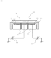
- FIG. 1 is a longitudinal sectional view showing the configuration of a plasma processing apparatus that performs a plasma processing method according to an embodiment of the present invention.
- FIG. 2 is a plan view schematically showing the dispersion plate according to the embodiment.
- FIG. 3 is a vertical cross-sectional view schematically showing the configuration of the sample stage according to the embodiment.
- FIG. 4 is a plan view schematically showing the configuration of the electrostatic attraction film 302 according to the embodiment.
- FIG. 5 is a vertical cross-sectional view schematically showing how a wafer is electrostatically attracted in the embodiment.
- FIG. 6 is a diagram showing a case where a positional shift occurs in the conventional technique.
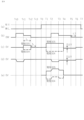
- FIG. 7 is a time chart showing the wafer processing method according to the embodiment.
- FIG. 8 is a diagram showing an electric circuit from plasma to ground.
- FIG. 9 is a timing chart showing a plasma processing method according to a modification of the embodiment.
- the term "upper surface” refers to the surface shown above in the drawing when a plate-like member or a cross section included in the plate-like member is illustrated. Further, the term “side surface” refers to a plate-like member or a surface in a cross section included in the plate-like member or a thickness of a layer.
- central axis means an axis that passes through the center of a circular surface and extends in a direction perpendicular to the surface.
- FIG. 1 is a longitudinal sectional view showing the configuration of a plasma processing apparatus that performs a plasma processing method according to an embodiment of the present invention.
- the plasma processing apparatus 100 of the embodiment includes a vacuum container 101.
- a processing chamber 104 which is a cylindrical space, is provided inside the vacuum container 101.
- the vacuum container 101 is connected to a vacuum pump 1015 such as a turbo molecular pump via a pressure regulating valve 1016.
- the vacuum pump 1015 exhausts particles in the processing chamber 104 and brings the processing chamber 104 to a predetermined atmospheric pressure.
- the pressure regulating valve 1016 has the function of changing the cross-sectional area of the passage connecting the vacuum pump 1015 and the processing chamber 104, and adjusting the flow rate or speed of exhaust gas.
- the vacuum container 101 includes a discharge chamber 102 on the upstream side of the processing chamber 104.
- the processing chamber 104 is connected via a dispersion plate 106 to the discharge chamber 102 where plasma generation is performed.
- the discharge chamber 102 and the processing chamber 104 are both cylindrical spaces.
- the central axis of the discharge chamber 102 and the central axis of the processing chamber 104 are located at a common axis or close enough to be considered to be a common axis.
- the dispersion plate 106 is provided between the discharge chamber 102 and the processing chamber 104, and partitions the discharge chamber 102 and the processing chamber 104. Specifically, the dispersion plate 106 is arranged in a passage connecting the discharge chamber 102 and the processing chamber 104.
- the passage between the discharge chamber 102 and the processing chamber 104 has a cylindrical shape
- the distribution plate 106 is a disc-shaped plate member having the same diameter as the passage. Details of the distribution plate 106 will be described later.
- a wafer to be processed is placed on the sample stage 103.
- the sample stage 103 is placed at a position facing the dispersion plate 106. Details of the sample stage 103 will be described later.
- the discharge chamber 102 is a space inside a dielectric chamber 107 made of a dielectric (quartz in the embodiment).
- a coil 108 is arranged on the outer peripheral side wall of the dielectric chamber 107 so as to surround the dielectric chamber 107 .
- the coil 108 is electrically connected to a high frequency power source 110 via a matching box 109, and is supplied with high frequency power from the high frequency power source 110.
- the high frequency power power in a frequency band of several tens of MHz such as 13.56 MHz is used.
- a top plate 1012 and a gas distribution plate 10121 are arranged at the upper end of the dielectric chamber 107.
- the top plate 1012 and the gas distribution plate 10121 define the inside and outside of the dielectric chamber 107.
- a passageway extending from a gas source 1013 is coupled to the top plate 1012 . Gas supplied from a gas source 1013 is introduced into the discharge chamber 102 via a gas distribution plate 10121.
- the gas source 1013 has a storage section for each type of gas to be supplied.
- a mass flow controller 1014 provided between the gas source 1013 and the top plate 1012 adjusts the amount of gas introduced into the discharge chamber 102 .
- the processing gas used in the embodiment includes a combustible gas, a combustion-supporting gas, a mixed gas thereof, or a gas diluted with an inert gas.
- the IR lamp unit 105 is arranged so as to surround the passage or the distribution plate 106 that connects the discharge chamber 102 and the processing chamber 104.
- the IR lamp unit 105 heats the sample stage 103, the wafer placed thereon, the inside of the processing chamber 104, etc. by irradiating electromagnetic waves.
- the IR lamp unit 105 is constituted by an IR lamp 1017 that emits electromagnetic waves including an infrared (Infra-Red: IR) band.
- the IR lamp unit 105 includes a reflector 1018 that reflects the IR light emitted from the IR lamp 1017 toward the processing chamber 104, and a reflector plate 1018 that processes the IR light emitted from the IR lamp 1017.
- An IR light transmitting window 1019 is provided that transmits toward the chamber 104 or the dispersion plate 106 .
- wafer processing is performed on a wafer placed on a sample stage 103.
- gas is first introduced into the discharge chamber 102.
- an induced magnetic field is formed at the center of the coil 108.
- ICP inductively coupled plasma
- Processing such as etching is performed using the generated plasma 1011 while heating with the IR lamp unit 105 or adjusting the temperature on the sample stage 103 (described later).
- etching plasma, static elimination plasma, and cleaning plasma are generated depending on the gas and high-frequency power used.
- FIG. 2 is a plan view schematically showing the dispersion plate 106 according to the embodiment. While the dispersion plate 106 shown in FIG. 1 is a cross-sectional view, the dispersion plate 06 shown in FIG. 2 is a view seen from above in FIG.
- the dispersion plate 106 is a circular plate-like member.
- the dispersion plate 106 has a plurality of through holes 201 that allow charged particles to move from the discharge chamber 102 to the processing chamber 104.
- Each of the plurality of through holes 201 is a circular hole.
- three circular holes are arranged from locations beyond a predetermined radius. Three holes are similarly arranged at positions shifted by 15 degrees in the circumferential direction.
- a plurality of through holes 201 are provided in a ring shape on the outer peripheral side of the dispersion plate 106.
- the dispersion plate 106 is made of a dielectric member such as quartz that is transparent. The material is not limited to quartz and can be selected as appropriate.
- neutral particles such as gas radicals contained in the plasma 1011 are uniformly introduced from the discharge chamber 102 into the processing chamber 104. That is, neutral particles such as radicals are introduced into the processing chamber 104 from a ring-shaped portion on the outer circumferential side of the dispersion plate 106, which is disposed at a position facing the wafer placed on the sample stage 103.
- the arrangement of the plurality of through holes 201 as described above is not limited to this.
- the arrangement of the through holes can be appropriately selected so that the distribution of neutral particles such as radicals that reach the surface of the wafer introduced into the processing chamber 104 provides a desired processing result for the film layer to be processed. Note that charged particles such as ions and electrons contained in the plasma 1011 are suppressed from being introduced from the discharge chamber 102 into the processing chamber 104 by the dispersion plate 106 .
- FIG. 3 is a vertical cross-sectional view schematically showing the configuration of the sample stage 103 according to the embodiment.
- FIG. 4 is a plan view schematically showing the configuration of the electrostatic attraction film 302 according to the embodiment.
- the wafer W is electrostatically attracted and processed in an apparatus including a processing chamber 104 and a sample stage 103 having an electrode capable of electrostatically adsorbing a wafer placed in the processing chamber 104.
- the sample stage 103 shown in FIG. 3 has a cylindrical shape.
- the central axis of the sample stage 103 and the central axis of the processing chamber 104 are located at a common axis or so close that they can be regarded as a common axis.
- the sample stage 103 includes a base material 301 made of a conductor such as metal, an electrostatic adsorption film 302 disposed on the base material 301, and a structure surrounding the side surfaces of the base material 301 and the electrostatic adsorption film 302.
- a susceptor ring 311 is provided.
- the wafer placed on the sample stage 103 will be placed on the electrostatic adsorption film 302.
- the electrostatic adsorption film 302 comes into contact with the wafer and grips the wafer by electrostatic adsorption.
- the electrostatic adsorption film 302 includes a sheet S made of polyimide resin.
- a sheet S made of polyimide resin is provided on the surface of the electrostatic adsorption film 302.
- the susceptor ring 311 is made of a dielectric material and has a function of protecting the base material 301 from the plasma 1011.
- the susceptor ring 311 of the embodiment has a shape that surrounds the side wall of the electrostatic adsorption film 302 on the upper part of the base material 301 and covers from the side wall of the base material 301 to the lower part of the base material 301.
- a refrigerant flow path 303 is arranged inside the base material 301. Refrigerant is supplied from the chiller 312 to the refrigerant flow path 303 , and the supplied refrigerant circulates through the refrigerant flow path 303 .
- the chiller 312 is arranged in a space below the floor of a building such as a clean room in which the plasma processing apparatus 100 is arranged, and is connected to the coolant flow path 303.
- the wafer placed on the sample stage 103 is adjusted to a desired temperature suitable for wafer processing by exchanging heat with the coolant flowing through the coolant flow path 303 via the electrostatic adsorption film 302 and the base material 301.
- the shape of the coolant flow path 303 may be, for example, arranged concentrically with respect to a central axis that is perpendicular to the surface direction of the base material 301, or arranged spirally. Good too.
- a plurality of grooves 308 are formed on the upper surface of the electrostatic attraction film 302.
- the heat transfer gas source 310 supplies a gas having heat transfer properties such as He gas through a path having a valve 309 that opens and closes.
- the gas supplied from the heat transfer gas source 310 diffuses along the groove 308 and reaches the back surface of the wafer W.
- the He gas filling the groove 308 promotes heat transfer between the coolant flowing through the coolant channel 303 and the wafer W, and the temperature of the wafer W is efficiently controlled.
- the surface of the electrostatic adsorption film 302 is constituted by a sheet S made of polyimide resin.
- the polyimide resin sheet S is a film made of a resin material containing polyimide.
- Polyimide resins are generally known to have a low coefficient of friction, wear resistance, and excellent insulation properties.
- the polyimide resin sheet S prevents scratches on the back side of the wafer due to expansion or contraction of the wafer, even if the temperature changes due to heating or cooling while the wafer is electrostatically attracted. There is a function to Note that the material of the sheet S is not limited to this, and can be selected as appropriate.
- FIG. 4 shows a cross-sectional structure when the electrostatic adsorption film 302 is cut in the plane direction.
- a plurality of film-like electrodes 304 and 305 are arranged inside the electrostatic adsorption film 302.
- DC power is supplied to the electrode 304 from a DC power supply 306, and DC power is supplied to the electrode 305 from a DC power supply 307.
- the electrodes 304 and 30 each have a plurality of arc-shaped arm portions arranged concentrically around the central axis in the plane direction of the sample stage 103, so that the arm of one electrode is connected to the other electrode. It has a so-called comb-like arrangement, sandwiched between the arms of the body. Note that the shapes of the electrodes 304 and 305 are not limited to this. Any material may be used as long as it is evenly distributed within the electrostatic adsorption film 302.
- FIG. 5 is a vertical cross-sectional view schematically showing how a wafer is electrostatically attracted in the embodiment.
- the sample stage 103 shown in FIG. 5 is the same as the sample stage 103 shown in FIG. 3.
- the constituent elements shown in FIG. 3 are omitted, and constituent elements not shown in FIG. 3 are also shown.
- the sizes of the configurations are shown changed to make it easier to understand.
- a ⁇ voltage is applied to the electrode 304 from a DC power source 306, and a + voltage is applied to the electrode 305 from a DC power source 307.
- a dipole electrode is formed between the electrodes 304 and 305.
- the + ions in the wafer W approach the - voltage electrode 304, and the - ions approach the + voltage electrode 305, respectively.
- Electrostatic forces are generated between the + ions in the wafer W and the electrode 304 and between the - ions in the wafer W and the electrode 305, and the wafer W is attracted to the sample stage 103.
- a voltage of -1500V is applied to the electrode 304 from a DC power supply 306, and a voltage of 1500V is applied to the other electrode 305 from a DC power supply 307.
- the voltage when a voltage of 1500V is applied to the electrode 304 by the DC power supply 306, the voltage may be adjusted so that a voltage of -1500V is applied to the electrode 305 from the DC power supply 307.
- the voltage from the DC power supplies 306 and 307 is ⁇ 1500V, and is adjusted so that voltages of the same magnitude and different polarity are applied from one DC power supply and the other DC power supply, but the present invention is not limited to this. . If the wafer W can be attracted onto the electrostatic adsorption film 302 and the occurrence and amount of positional deviation can be kept within the permissible range when holding or attaching or removing the wafer W, a voltage exceeding ⁇ 1500 V or less may be used. Even if it is used, the absolute value of the voltage applied to each electrode does not have to be the same. Further, the electrodes 304 and 305 may be given the same polarity.
- the plasma processing apparatus 100 extends from the inside of the sample stage 103 toward the top surface of the sample stage 103.
- a plurality of (for example, three) push-up pins 313 are provided. After the electrostatic adsorption of the wafer W is released, the push-up pins 313 housed inside the sample stage 103 move upward and push up the wafer W, thereby making it possible to remove the wafer W from the sample stage 103. can.
- the detached wafer W is held by a transfer mechanism such as a robot arm and carried out from the processing chamber 104.
- FIG. 6 is a diagram showing a case where a positional shift occurs in the conventional technique.
- the first phenomenon is caused by charged particles generated during processing.
- the electrostatic adsorption film 302 may be damaged by collisions with charged particles such as ions, or may have reaction products attached thereto.
- power is generally not supplied to the electrodes 304 and 305 in the electrostatic attraction film 302 during waferless plasma processing.
- charged particles such as ions adhere to the electrostatic adsorption film 302 they will be removed as shown in FIG. , remains on the surface of the electrostatic adsorption film 302 as a negative charge.
- the potential of the surface of the electrostatic adsorption film 302 was detected before and during waferless plasma processing using the plasma processing apparatus 100, and as a result, it was found that the potential varied before and after the processing. There was found. From this, as described above, it is assumed that charges exist in the electrostatic adsorption film 302 in the process of processing using waferless plasma.
- the second phenomenon is caused by the dispersion plate 106.
- the dispersion plate 106 can prevent charged particles such as ions from moving to the processing chamber 104 at locations where the through holes 201 are not arranged, some of the charged particles may pass through the locations where the through holes 201 are arranged and enter the discharge chamber. 102 and flows into the processing chamber 104 . Due to the nature of the distribution of the through holes, a relatively large amount of the charged particles that have flowed in adhere to the outer peripheral portion of the surface of the electrostatic adsorption film 302.
- the wafer W is electrostatically attracted to the sample stage 103 with charged particles attached to it in this way, there is a possibility that partial adsorption, in which a large electrostatic adsorption force acts locally on a portion of the back surface of the wafer W, may occur.
- the wafer W is partially attracted, even if the static elimination step after the plasma treatment shown in the prior art is performed, the charge in the electrostatic adsorption film 302 is not sufficiently reduced and the electrostatic force remains. Therefore, residual adsorption force acts on the wafer W, making it difficult to detach the wafer W from the sample stage 103, and there is a risk that a large force will be applied during detachment, causing damage or misalignment of the wafer W. be.
- the third phenomenon is caused by the sheet S made of polyimide resin.
- the wafer mounting surface of the electrostatic adsorption film 302 is constituted by a sheet S made of polyimide resin. It is generally known that highly insulating substances such as polyimide resin have properties that make it difficult to conduct electricity and that charged particles tend to remain. Therefore, the electric charge cannot be sufficiently removed only by performing the static elimination step shown in the prior art.
- FIG. 7 is a time chart showing the wafer processing method according to the embodiment.
- FIG. 7A shows the presence or absence of the wafer W on the sample stage 103.
- FIG. 7B shows the output (power) of the high-frequency power source 110 that supplies high-frequency power for forming the plasma 1011 to the coil 108.
- FIG. 7(c) shows the potentials of electrodes 304 and 305.
- FIG. 7(d) shows the potential on the surface of the wafer W or the electrostatic attraction film 302.
- FIG. 7E shows the potential difference between the electrode 304 and the wafer W or the potential difference between the electrode 305 and the wafer W.
- a wafer-less static elimination process is performed to remove charged particles remaining on the electrostatic adsorption film 302.
- the wafer-less static elimination process is performed in a so-called wafer-less state where there is no member covering the upper surface of the sample stage 103 on which the wafer is placed. As shown in FIG. 7A, the waferless state continues from time Tp0 to time Tp2.
- FIG. 7E showing the potential difference, no potential is shown in the static elimination process from Tp0 to Tp2.
- the plasma 1011 is formed in the discharge chamber 102, charged particles such as generated ions enter the processing chamber 104 and adhere to the surface of the electrostatic adsorption film 302 of the sample stage 103. Therefore, the potential from time Tp0 to time Tp2 in FIG. 7(d) indicates the potential of the electrostatic attraction film 302.
- a wafer-less charge removal process is performed in which the charges accumulated on the sample stage 103 are removed without placing a wafer on the sample stage 103.
- first static elimination gas for generating static elimination plasma
- a gas such as SF 6 that is reactive with deposits or an inert gas such as Ar is used. It will be done.
- a static eliminating gas a gas that causes less damage to the polyimide resin, which is a material forming the electrostatic adsorption film 302, is selected. Note that such gases include gases that have not only a static eliminating effect but also a cleaning effect of removing reaction products and the like attached to the processing chamber 104.
- a plasma generation step is performed in which plasma is generated using the first static elimination gas.
- plasma is generated from the first static elimination gas in the discharge chamber 102 using high frequency power.
- high frequency power hereinafter also referred to as "first high frequency power”
- first high frequency power is supplied from the high frequency power supply 110 to the coil 108.
- the first static elimination gas introduced in advance exists in the discharge chamber 102.
- a power supply step is performed in which first power is supplied to the electrodes 304 and 305 of the sample stage 103.
- first power is supplied to the electrodes 304 and 305 of the sample stage 103.
- 100V is applied from the DC power supply 306 to the electrode 304
- -100V is applied to the electrode 305 from the DC power supply 307.
- FIG. 8 is a diagram showing an electric circuit from plasma to ground.
- the dashed line indicates the flow of charge.
- Charged particles generated in plasma 1011 reach the ground connected to DC power source 306 or 307 via electrostatic adsorption film 302, electrode 304 or 305, push-up pin 313, and base material 301. Further, the charges generated in the plasma 1011 directly adhere to the push-up pin 313 and reach the ground connected to the base material 301 and the DC power source 306 or 307. It is assumed that the charged particles attached to the electrostatic adsorption film 302 reach the ground in this way.
- time Tp1 refers to the time when the charged particles remaining in the processing chamber 104 disappear. Therefore, time Tp1 may be extended to time Tp02, which is delayed by a period t1 until the afterglow discharge of plasma 1011 disappears.
- a wafer processing process is performed in which the wafer W placed on the sample stage 103 is electrostatically attracted and the wafer W is processed.
- the wafer processing process includes a wafer etching process and a static elimination process while the wafer is being placed.
- the wafer processing step includes a mounting step, an electrostatic adsorption step, and a plasma etching step, and the static elimination step during wafer mounting includes a static elimination plasma generation step and a potential difference reduction step.
- a mounting step is performed in which the wafer W is mounted on the sample stage 103.
- the wafer W is carried into the processing chamber 104 by a transfer mechanism such as a robot arm and placed on the sample stage 103.
- an electrostatic adsorption step is performed in which second power is supplied to the electrodes 304 and 305 of the sample stage 103 to electrostatically adsorb the wafer W.
- second power is supplied to the electrodes 304 and 305 of the sample stage 103 to electrostatically adsorb the wafer W.
- a voltage is applied to the electrodes 304 and 305, and the wafer W is electrostatically attracted onto the electrostatic adsorption film 302.
- the voltage applied to the electrode 304 and the voltage applied to the electrode 305 are adjusted to have different polarities and equal absolute values. As described above, for example, -1500V is applied to electrode 304 and 1500V is applied to electrode 305.
- a plasma etching process is performed in which a processing gas is supplied to the discharge chamber 102 and plasma is generated from the processing gas using second high-frequency power.
- the second high frequency power is supplied from the high frequency power supply 110 to the coil 108, as shown in FIG. 7(b).
- etching plasma 1011 is generated from the processing gas introduced into the discharge chamber 102.
- Reactive particles such as radicals that have passed through the dispersion plate 106 react with the film layer to be processed on the surface of the wafer W, and plasma etching progresses.
- a static electricity removal process is performed while the wafer is being placed.
- the static elimination process during wafer placement is a process of supplying the second static elimination gas to the discharge chamber 102 and generating plasma from the second static elimination gas using the third high-frequency power.
- the high frequency power supplied from the high frequency power supply 110 to the coil 108 is changed to a high frequency power (hereinafter referred to as "third high frequency power") different from the second high frequency power during the etching process. ).
- the gas introduced into the discharge chamber 102 is switched from the processing gas to a static elimination gas (hereinafter referred to as "second static elimination gas") that has less influence on the wafer W, such as an inert gas.
- second static elimination gas a static elimination plasma generation step is performed in which the static elimination plasma 1011 is generated from the second static elimination gas using the third high-frequency power.
- a potential difference reduction step is performed in which a second power is applied so that the electrodes 304 and 305 of the sample stage 103 have a potential equal to the potential of the wafer W.
- the voltage applied to the electrodes 304 and 305 as the supplied second power is - ⁇ V, which is equal to the potential of the wafer W.
- the potential of the wafer W can be determined in advance.
- the potential of the wafer W may be measured after the plasma 1011 for static elimination is generated after time T3.
- Time T6 when a predetermined time t2 has elapsed from time T5, represents the time when the charged particles remaining in the processing chamber 104 disappear.
- the predetermined time t2 may be a time until the afterglow discharge of the static elimination plasma 1011 disappears.
- the resistance value of the electrostatic adsorption film 302 is sufficiently large, the potential of the wafer W is changed by the plasma treatment for static elimination starting from time T3, as shown in FIG. 7(d).
- the middle value - ⁇ V is maintained as is.
- the potentials of electrodes 304 and 305 are also unchanged from time T4.
- the potential difference between the wafer W and the electrode 304 and the potential difference between the wafer W and the electrode 305 remain at 0V from time T4 as shown in FIG. There is no electrostatic adsorption force between the two.
- the voltage applied to the electrodes 304 and 305 is set to 0V.
- the potential of the electrodes 304 and 305 changes, and the potential of the wafer W also changes following the change in the potential of the electrodes 304 and 305, and becomes approximately 0V.
- the potential difference between the wafer W and the electrode 304 and the potential difference between the wafer W and the electrode 305 are maintained at approximately 0V even after T6. That is, the potentials of the electrodes 304 and 305 can be set to 0V in a state where the electrostatic attraction force between the wafer W and the electrode 304 and the electrostatic attraction force between the wafer W and the electrode 305 are eliminated.
- the wafer W is removed from the sample stage 103 by the push-up pins 313 and carried out to the outside of the processing chamber 104.
- first power, the second power, the first high frequency power, the second high frequency power, and the third high frequency power can be appropriately set according to the manufacturing conditions and the purpose of the process. It is also possible to use the same type of gas for the first static elimination gas and the second static elimination gas, or it is also possible to use different types of gas. Furthermore, the size of the time in the time chart can also be set as appropriate.
- FIG. 9 is a timing chart showing a plasma processing method according to a modification of the embodiment.
- FIG. 9A shows the presence or absence of the wafer W on the sample stage 103.
- FIG. 9B shows the output (power) of the high frequency power supply 110 that supplies high frequency power for forming the plasma 1011 to the coil 108.
- FIG. 9(c) shows the potentials of the electrostatic adsorption electrodes 304 and 305.
- FIG. 9(d) shows the potential on the surface of the wafer W or the electrostatic attraction film 302.
- FIG. 9E shows the potential difference between the electrode 304 and the wafer W and the potential difference between the electrode 305 and the wafer W.
- the modified example differs from the embodiment in that a static elimination process is performed after cleaning.
- differences appear between FIG. 9(b), FIG. 9(c), and FIG. 9(d).
- the same reference numerals are given to the same or equivalent components as in the above-described embodiment, and the description thereof will be simplified or omitted.
- a step of cleaning the discharge chamber 102 and the processing chamber 104 is performed without a wafer.
- high frequency power hereinafter also referred to as "fourth high frequency power”
- cleaning gas is introduced into the discharge chamber 102.
- a gas that causes little damage to the polyimide resin such as SF 6 gas and Ar gas, is selected. In this way, plasma 1011 for performing cleaning is generated.
- a post-cleaning static elimination process for reducing the charge on the electrostatic adsorption film 302 will be described.
- plasma 1011 for static elimination is generated.
- the high frequency power supplied from the high frequency power supply 110 to the coil 108 is a high frequency power (hereinafter also referred to as "fifth high frequency power") that is different from the fourth high frequency power during cleaning.
- Change to The fifth high frequency power is, for example, 1000W.
- the gas introduced into the discharge chamber 102 is switched from a cleaning gas to a static elimination gas (hereinafter also referred to as "third static elimination gas") such as an inert gas such as Ar gas.
- a static elimination plasma generation procedure is performed in which the static elimination plasma 1011 is generated from the third static elimination gas using the fifth high-frequency power.
- a residual charge removal step is performed in which third power is supplied to the electrodes 304 and 305 of the sample stage 103.
- the third power supplied for example, 100V is applied from the DC power supply 306 to the electrode 304, and -100V is applied to the electrode 305 from the DC power supply 307. These voltages are lower than the voltages applied when electrostatically adsorbing the wafer W.
- the time when the high frequency power is changed to generate the plasma for static elimination and the time when the voltage is applied to the electrodes 304 and 305 are not limited to the same time. As shown in FIG. 9B, application of voltage to the electrodes 304 and 305 may be started within the time ta between time Tc1 and time Tc2 when plasma 1011 for static elimination is formed. Furthermore, after applying the voltage to the electrodes 304 and 305, the high frequency power may be changed to generate the plasma 1011 for static elimination. In any case, it is necessary that the period during which the static elimination plasma 1011 is generated and the period during which the voltage is applied to the electrodes 304 and 305 at least overlap, and in a modified example, the periods overlap by 1 second or more.
- the power supply from the high frequency power supply 110 to the coil 108 is stopped as shown in FIG. 9(b). Further, as shown in FIG. 9(c), the voltage applied to the electrodes 304 and 305 is set to 0V. Similar to the embodiment, the period from time Tc1 to time Tc2 is a period in which charged particles remaining in the processing chamber 104 are sufficiently removed, and is a period in which the afterglow discharge of the static elimination plasma 1011 disappears. It may be extended by tb.
- the post-cleaning static elimination process ends. Thereafter, the wafer W is transferred to the processing chamber 104, and a predetermined wafer processing process is performed.
- the wafer processing process is the same as in the embodiment.
- the fourth high-frequency power, the fifth high-frequency power, the third static elimination gas, and the third power can be appropriately set according to the manufacturing conditions and the purpose of the process, as in the embodiment. Furthermore, the size of the time in the time chart can also be set as appropriate.
- the inventors conducted experiments and studied the relationship between the voltage applied to the electrodes 304 and 305, the voltage application time, and the static elimination effect in the static elimination step of reducing the charge on the electrostatic adsorption film 302.
- the power of the high-frequency power source 110 set to 1000 W
- the voltage applied to the electrodes 304 and 305 set to a value in the range of ⁇ 100 V to ⁇ 500 V
- the electrostatic adsorption film 302 was sufficiently strong. It was confirmed that the static electricity was removed and the positional shift when the wafer W was attached to and detached from the sample stage 103 was suppressed.
- the polarities of the voltages applied to the electrodes 304 and 305 are different, but even if the polarities are the same, the same static elimination effect can be achieved.
- the output of the high frequency power source 110 may be changed, or the electrostatic attraction film 302 made of another highly insulating material may be used. Further, in accordance with these changes, the value of the voltage applied to the electrodes 304 and 305 and the time of the process can be appropriately changed.
- inductively coupled plasma 1011 is formed, and the present invention is applicable regardless of the plasma generation method.
- the present invention is applicable to a helicon wave plasma processing apparatus, an ECR plasma processing apparatus using microwaves, a capacitively coupled plasma processing apparatus, and the like.
- Plasma processing apparatus 101... Vacuum vessel 102... Discharge chamber 103... Sample stand 104... Processing chamber 105... IR lamp unit 106... Dispersion plate 107... Dielectric material Chamber 108... Coil 109... Matching box 110... High frequency power supply 201... Through holes 301, 301a... Base material 302, 302a... Electrostatic adsorption film 303... Refrigerant circuit 304, 305... ... Electrodes 306, 307 ... DC power supply 308 ... Groove 309 ... Valve 310 ... Heat transfer gas source 311 ... Susceptor ring 312 ... Chiller 313 ... Push-up pin 1011 ... Plasma 1012...Top plate 10121...Gas distribution plate 1014...Mass flow controller 1015...Vacuum pump 1016...Pressure regulating valve 1017...IR lamp 1018...Reflector plate 1019...IR light transmission window
Abstract
The purpose of the present invention is to provide a method for wafer treatment, the method making it possible to inhibit wafer-position shifting in wafer treatments. This method for wafer treatment comprises: a wafer-less charge removal step in which, in a treatment device equipped with a sample table having an electrode capable of electrostatically holding a wafer, any charge accumulated on the sample table is removed, with the sample table having no wafer placed thereon; and a wafer treatment step in which after the wafer-less charge removal step, a wafer placed on the sample table is electrostatically held thereon and the wafer is treated. The wafer-less charge removal step comprises a plasma generation step in which a plasma is generated using a first gas for charge removal and a power supply step in which first electric power is supplied to the electrode of the sample table.
Description
本発明は、ウエハ処理方法に関する。
The present invention relates to a wafer processing method.
近年、半導体デバイスの市場では低消費電力や記憶容量増大が求められており、これら要件を実現するため、3次元構造を持つ半導体デバイスの開発に関心が集まっている。3次元構造を加工する方法のひとつとして、異方性または等方性いずれかのエッチングを用途に応じて選択することが可能なプラズマエッチングが採用されている。
In recent years, there has been a demand for lower power consumption and increased storage capacity in the semiconductor device market, and in order to meet these requirements, there is growing interest in the development of semiconductor devices with a three-dimensional structure. As one method for processing a three-dimensional structure, plasma etching is employed, in which either anisotropic or isotropic etching can be selected depending on the application.
プラズマを用いてエッチング処理をする過程において、例えば被加工材料とラジカルの間において、反応生成物が発生する。反応生成物が処理室内に付着あるいは堆積すると、プラズマ処理装置のエッチング性能に様々な問題をもたらすことが知られている。
In the process of etching using plasma, reaction products are generated, for example, between the material to be processed and radicals. It is known that adhesion or accumulation of reaction products within a processing chamber causes various problems in the etching performance of a plasma processing apparatus.
これら問題の対策として、定期的なクリーニング処理によって反応生成物を除去することが提案されている。特開2002-217166号公報(特許文献1)には、真空容器内の堆積物をプラズマ処理により除去するプラズマクリーニング方法や、プラズマを用いずにガス導入によりクリーニングを実施するガスクリーニング方法が記載されている。これらのクリーニングでは、ガスやプラズマから静電吸着面や電極を保護するため、試料台の上にダミーウエハを載置した状態でクリーニングが実施される。
As a countermeasure to these problems, it has been proposed to remove reaction products through periodic cleaning treatments. Japanese Unexamined Patent Publication No. 2002-217166 (Patent Document 1) describes a plasma cleaning method in which deposits in a vacuum container are removed by plasma treatment, and a gas cleaning method in which cleaning is performed by introducing gas without using plasma. ing. In these cleanings, in order to protect the electrostatic attraction surface and electrodes from gas and plasma, cleaning is performed with a dummy wafer placed on the sample stage.
また、特開2021-204644号公報(特許文献2)には、真空容器内及び特に試料台の周辺を対象としたクリーニング方法として、ダミーウエハを載置しないウエハレスでのクリーニング方法が開示されている。この方法では、O2ガスによるプラズマを用い、試料台の上にダミーウエハを載置せずにプラズマクリーニングを実施することが示されている。
Furthermore, Japanese Patent Laid-Open No. 2021-204644 (Patent Document 2) discloses a waferless cleaning method in which a dummy wafer is not placed, as a cleaning method targeting the inside of a vacuum container and especially around the sample stage. In this method, it has been shown that plasma cleaning is performed using O 2 gas plasma without placing a dummy wafer on the sample stage.
特許文献1では、下部電極を保護するためにダミーウエハが載置されるところ、下部電極を有する試料台に残留する荷電粒子の影響は考慮されていない。また、特許文献2に記載されているように、ウエハレスの状態でプラズマを形成して処理室内のクリーニング処理をする場合、プラズマにより生成されたイオン等の荷電粒子が試料台に付着する。
このように、上記先行技術は、いずれも試料台に荷電粒子が残留する場合について十分な考慮がなされていない。 In Patent Document 1, a dummy wafer is placed to protect the lower electrode, but the influence of charged particles remaining on the sample stage having the lower electrode is not considered. Further, as described inPatent Document 2, when plasma is formed in a waferless state to perform a cleaning process inside a processing chamber, charged particles such as ions generated by the plasma adhere to the sample stage.
As described above, the above-mentioned prior art does not give sufficient consideration to the case where charged particles remain on the sample stage.
このように、上記先行技術は、いずれも試料台に荷電粒子が残留する場合について十分な考慮がなされていない。 In Patent Document 1, a dummy wafer is placed to protect the lower electrode, but the influence of charged particles remaining on the sample stage having the lower electrode is not considered. Further, as described in
As described above, the above-mentioned prior art does not give sufficient consideration to the case where charged particles remain on the sample stage.
試料台に荷電粒子が残留した状態でウエハが載置された場合、当該ウエハに電荷に起因する力が作用して、ウエハが当初の載置された箇所からずれる位置ずれが発生する虞がある。ウエハの位置ずれは、半導体デバイスを製造するときの効率や歩留まりを損なう要因のひとつとなっていた。
If a wafer is placed on the sample stage with charged particles remaining, there is a risk that force due to the charge will act on the wafer, causing the wafer to shift from its original placement. . Wafer misalignment has been one of the factors that impairs efficiency and yield when manufacturing semiconductor devices.
本発明は、ウエハ処理におけるウエハの位置ずれを抑制することを可能とするウエハ処理方法を提供することを目的とする。
An object of the present invention is to provide a wafer processing method that makes it possible to suppress misalignment of a wafer during wafer processing.
上記の課題を解決するために、本発明のウエハ処理方法は、ウエハを静電吸着可能な電極を有する試料台を備えた処理装置において、前記試料台にウエハを載置せずに前記試料台に帯電した電荷を除去するウエハレスの除電工程と、前記ウエハレスの除電工程の後に、前記試料台に載置したウエハを静電吸着し、前記ウエハに処理を施すウエハ処理工程と、を含む。
In order to solve the above problems, the wafer processing method of the present invention provides a processing apparatus equipped with a sample stage having an electrode capable of electrostatically adsorbing a wafer. A wafer-less static elimination process for removing charges accumulated in the wafer, and a wafer processing process for electrostatically adsorbing the wafer placed on the sample stage and processing the wafer after the wafer-less static elimination process.
本発明によれば、ウエハ処理におけるウエハの位置ずれを抑制することを可能とするウエハ処理方法を提供することができる。
According to the present invention, it is possible to provide a wafer processing method that makes it possible to suppress misalignment of a wafer during wafer processing.
以下、本発明の実施の形態について、図面を用いて説明する。
なお、この実施形態により本発明が限定されるものではない。また、図面の記載において、同一部分には同一の符号を付して示している。
同一あるいは同様の機能を有する構成要素が複数ある場合には、同一の符号に異なる添字を付して説明する場合がある。また、これらの複数の構成要素を区別する必要がない場合には、添字を省略して説明する場合がある。
図面において示す各構成要素の位置、大きさ、形状、範囲などは、発明の理解を容易にするため、実際の位置、大きさ、形状、範囲などを表していない場合がある。このため、本発明は、必ずしも、図面に開示された位置、大きさ、形状、範囲などに限定されない。 Embodiments of the present invention will be described below with reference to the drawings.
Note that the present invention is not limited to this embodiment. In addition, in the description of the drawings, the same parts are denoted by the same reference numerals.
When there are multiple components having the same or similar functions, the same reference numerals may be given different suffixes for explanation. Furthermore, if there is no need to distinguish between these multiple components, the subscripts may be omitted in the description.
The position, size, shape, range, etc. of each component shown in the drawings may not represent the actual position, size, shape, range, etc. in order to facilitate understanding of the invention. Therefore, the present invention is not necessarily limited to the position, size, shape, range, etc. disclosed in the drawings.
なお、本開示において、「上面」とは、板状部材や板状部材に含まれる断面を図示した場合の、図面上の上方に示される面を意味する。また、「側面」とは、板状部材や板状部材に含まれる断面における面や層の厚みの部分を意味する。
In the present disclosure, the term "upper surface" refers to the surface shown above in the drawing when a plate-like member or a cross section included in the plate-like member is illustrated. Further, the term "side surface" refers to a plate-like member or a surface in a cross section included in the plate-like member or a thickness of a layer.
また、「中心軸」とは、円盤状または円筒状の物体の場合、円形を有する面の中心を通り、面に垂直な方向に延びる軸を意味する。
Furthermore, in the case of a disc-shaped or cylindrical object, the term "central axis" means an axis that passes through the center of a circular surface and extends in a direction perpendicular to the surface.
[実施形態]
(装置の構成)
図1を用いて、本発明の実施形態に係るプラズマ処理方法を行うプラズマ処理装置の構成について説明する。図1は、本発明の実施形態に係るプラズマ処理方法を行うプラズマ処理装置の構成を示す縦断面図である。 [Embodiment]
(Device configuration)
The configuration of a plasma processing apparatus that performs a plasma processing method according to an embodiment of the present invention will be described with reference to FIG. FIG. 1 is a longitudinal sectional view showing the configuration of a plasma processing apparatus that performs a plasma processing method according to an embodiment of the present invention.
実施形態のプラズマ処理装置100は、真空容器101を備えている。真空容器101の内部には、円筒形状の空間である処理室104が設けられている。真空容器101は、調圧バルブ1016を介してターボ分子ポンプ等の真空ポンプ1015と接続される。真空ポンプ1015は、処理室104にある粒子を排出し、処理室104を所定の気圧にする。調圧バルブ1016は、真空ポンプ1015と処理室104を接続する通路の断面積を変更し、排気の流量または速度を調節する機能を有する。
The plasma processing apparatus 100 of the embodiment includes a vacuum container 101. A processing chamber 104, which is a cylindrical space, is provided inside the vacuum container 101. The vacuum container 101 is connected to a vacuum pump 1015 such as a turbo molecular pump via a pressure regulating valve 1016. The vacuum pump 1015 exhausts particles in the processing chamber 104 and brings the processing chamber 104 to a predetermined atmospheric pressure. The pressure regulating valve 1016 has the function of changing the cross-sectional area of the passage connecting the vacuum pump 1015 and the processing chamber 104, and adjusting the flow rate or speed of exhaust gas.
真空容器101は、処理室104の上流側に放電室102を備える。処理室104は、プラズマ生成が行われる放電室102と分散板106を介して接続する。放電室102と処理室104とは、共に円筒形状を有した空間である。放電室102の中心軸と処理室104の中心軸は、共通の軸であるかまたは共通の軸と見なせる程度に近似した位置にある。
The vacuum container 101 includes a discharge chamber 102 on the upstream side of the processing chamber 104. The processing chamber 104 is connected via a dispersion plate 106 to the discharge chamber 102 where plasma generation is performed. The discharge chamber 102 and the processing chamber 104 are both cylindrical spaces. The central axis of the discharge chamber 102 and the central axis of the processing chamber 104 are located at a common axis or close enough to be considered to be a common axis.
分散板106は、放電室102と処理室104の間に設けられており、放電室102と処理室104の間を区分する。分散板106は、具体的にいうと放電室102と処理室104の間を接続する通路内に配置される。実施形態において、放電室102と処理室104の間にある通路は円筒状の形状を有しており、分散板106は通路の径と同じ径を持つ円盤状の板状部材である。分散板106の詳細については後述する。
The dispersion plate 106 is provided between the discharge chamber 102 and the processing chamber 104, and partitions the discharge chamber 102 and the processing chamber 104. Specifically, the dispersion plate 106 is arranged in a passage connecting the discharge chamber 102 and the processing chamber 104. In the embodiment, the passage between the discharge chamber 102 and the processing chamber 104 has a cylindrical shape, and the distribution plate 106 is a disc-shaped plate member having the same diameter as the passage. Details of the distribution plate 106 will be described later.
試料台103は、処理対象のウエハが載置される。実施形態においては、試料台103は分散板106と対向する位置に配置される。試料台103の詳細については後述する。
A wafer to be processed is placed on the sample stage 103. In the embodiment, the sample stage 103 is placed at a position facing the dispersion plate 106. Details of the sample stage 103 will be described later.
放電室102は、誘電体(実施形態では石英)によって構成される誘電体チャンバ107の内部にある空間である。誘電体チャンバ107の外周側壁には、誘電体チャンバ107を囲むようにコイル108が配置される。コイル108は、整合器109を介して高周波電源110に電気的に接続されており、高周波電源110から高周波電力が供給される。高周波電力には、13.56MHzなど数十MHzの周波数帯の電力が用いられる。
The discharge chamber 102 is a space inside a dielectric chamber 107 made of a dielectric (quartz in the embodiment). A coil 108 is arranged on the outer peripheral side wall of the dielectric chamber 107 so as to surround the dielectric chamber 107 . The coil 108 is electrically connected to a high frequency power source 110 via a matching box 109, and is supplied with high frequency power from the high frequency power source 110. As the high frequency power, power in a frequency band of several tens of MHz such as 13.56 MHz is used.
誘電体チャンバ107の上端部には、天板1012およびガス分散板10121が配置されている。天板1012とおよびガス分散板10121によって、誘電体チャンバ107の内側と外側が区画される。天板1012には、ガス源1013から延びる通路が結合されている。ガス源1013から供給されるガスは、ガス分散板10121を介して放電室102に導入される。
A top plate 1012 and a gas distribution plate 10121 are arranged at the upper end of the dielectric chamber 107. The top plate 1012 and the gas distribution plate 10121 define the inside and outside of the dielectric chamber 107. A passageway extending from a gas source 1013 is coupled to the top plate 1012 . Gas supplied from a gas source 1013 is introduced into the discharge chamber 102 via a gas distribution plate 10121.
ガス源1013は、供給するガスの種類毎に貯留部を有している。ガス源1013と天板1012との間に設けられたマスフローコントローラ1014によって、放電室102へ導入するガスの供給量が調節される。実施形態において用いられる処理用のガスは、可燃性ガス、支燃性ガス、及びこれらの混合ガスを含むもの、あるいはこれらのガスを不活性ガスにより希釈したものである。
The gas source 1013 has a storage section for each type of gas to be supplied. A mass flow controller 1014 provided between the gas source 1013 and the top plate 1012 adjusts the amount of gas introduced into the discharge chamber 102 . The processing gas used in the embodiment includes a combustible gas, a combustion-supporting gas, a mixed gas thereof, or a gas diluted with an inert gas.
IRランプユニット105は、放電室102と処理室104との間を接続する通路または分散板106の周囲を囲うように配置される。IRランプユニット105は電磁波を照射することによって、試料台103またはこれに載置されたウエハ、処理室104の内部等を加熱する。実施形態では、IRランプユニット105は、赤外線(Infra-Red:IR)帯を含む電磁波を放射するIRランプ1017によって構成される。IRランプユニット105には、IRランプ1017に加えて、IRランプ1017から放射されたIR光を処理室104の方向に向けて反射する反射板1018、さらにIRランプ1017から放射されたIR光を処理室104または分散板106の方へ向けて透過するIR光透過窓1019を備える。
The IR lamp unit 105 is arranged so as to surround the passage or the distribution plate 106 that connects the discharge chamber 102 and the processing chamber 104. The IR lamp unit 105 heats the sample stage 103, the wafer placed thereon, the inside of the processing chamber 104, etc. by irradiating electromagnetic waves. In the embodiment, the IR lamp unit 105 is constituted by an IR lamp 1017 that emits electromagnetic waves including an infrared (Infra-Red: IR) band. In addition to the IR lamp 1017, the IR lamp unit 105 includes a reflector 1018 that reflects the IR light emitted from the IR lamp 1017 toward the processing chamber 104, and a reflector plate 1018 that processes the IR light emitted from the IR lamp 1017. An IR light transmitting window 1019 is provided that transmits toward the chamber 104 or the dispersion plate 106 .
プラズマ処理装置100では、試料台103に載置されるウエハに対してウエハ処理が行われる。ウエハ処理としては、まず、放電室102にガスを導入する。次に、コイル108に高周波電力を供給することにより、コイル108の中心に誘導磁場が形成される。誘導磁場が発生すると、放電室102にあるガスの粒子が励起されて放電が起こり、粒子が電離、解離して誘導結合型のプラズマ(ICP)1011が生成される。IRランプユニット105による加熱、または後述する試料台103における置ける温度調整などを行いつつ、発生したプラズマ1011によってエッチング等の加工が行われる。なお、実施形態においては、用いるガスおよび高周波電力に応じて、エッチング用のプラズマ、除電用のプラズマ、クリーニング用のプラズマが生成される。
In the plasma processing apparatus 100, wafer processing is performed on a wafer placed on a sample stage 103. For wafer processing, gas is first introduced into the discharge chamber 102. Next, by supplying high frequency power to the coil 108, an induced magnetic field is formed at the center of the coil 108. When the induced magnetic field is generated, gas particles in the discharge chamber 102 are excited and discharge occurs, the particles are ionized and dissociated, and an inductively coupled plasma (ICP) 1011 is generated. Processing such as etching is performed using the generated plasma 1011 while heating with the IR lamp unit 105 or adjusting the temperature on the sample stage 103 (described later). In the embodiment, etching plasma, static elimination plasma, and cleaning plasma are generated depending on the gas and high-frequency power used.
(分散板の構成)
ここで、図2を用いて分散板106の構成について説明する。図2は、実施形態に係る分散板106を模式的に示した平面図である。図1に示される分散板106は断面図であるところ、図2に示される分散版06は、図1の上方から見た図である。 (Configuration of distribution plate)
Here, the configuration of thedispersion plate 106 will be explained using FIG. 2. FIG. 2 is a plan view schematically showing the dispersion plate 106 according to the embodiment. While the dispersion plate 106 shown in FIG. 1 is a cross-sectional view, the dispersion plate 06 shown in FIG. 2 is a view seen from above in FIG.
ここで、図2を用いて分散板106の構成について説明する。図2は、実施形態に係る分散板106を模式的に示した平面図である。図1に示される分散板106は断面図であるところ、図2に示される分散版06は、図1の上方から見た図である。 (Configuration of distribution plate)
Here, the configuration of the
分散板106は、図2に示されるように、円形状を有した板状部材である。分散板106は、放電室102から処理室104へ荷電粒子の移動を可能とする複数の貫通孔201を有する。複数の貫通孔201の各々は円形の孔である。分散板106の中心から半径方向を考える場合、所定の半径を超えた箇所から3つの円形の孔が配置されている。周方向に15°ずつ移動した位置にも同様に3つの孔が配置されている。言い換えると、分散板106の外周側において、複数の貫通孔201がリング状に設けられている。実施形態において、分散板106は、透光性を有した石英等の誘電体製の部材から構成されている。材料は石英に限定されず、適宜選択しうる。
As shown in FIG. 2, the dispersion plate 106 is a circular plate-like member. The dispersion plate 106 has a plurality of through holes 201 that allow charged particles to move from the discharge chamber 102 to the processing chamber 104. Each of the plurality of through holes 201 is a circular hole. When considering the radial direction from the center of the dispersion plate 106, three circular holes are arranged from locations beyond a predetermined radius. Three holes are similarly arranged at positions shifted by 15 degrees in the circumferential direction. In other words, a plurality of through holes 201 are provided in a ring shape on the outer peripheral side of the dispersion plate 106. In the embodiment, the dispersion plate 106 is made of a dielectric member such as quartz that is transparent. The material is not limited to quartz and can be selected as appropriate.
これら複数の貫通孔201を通じて、プラズマ1011に含まれるガスのラジカル等の中性粒子は、放電室102から処理室104に均一に導入される。すなわち、ラジカル等の中性粒子は、試料台103上に載せられるウエハに対向した位置に配置された分散板106の外周側のリング状の箇所から処理室104へ導入される。上記のような複数の貫通孔201の配置は、これに限定されない。処理室104に導入されるウエハの表面に到達するラジカル等の中性粒子の分布が、処理対象の膜層の処理結果が所望のものとなるように、貫通孔の配置は適宜選択されうる。なお、プラズマ1011に含まれるイオンや電子等の荷電粒子は、分散板106によって、放電室102から処理室104へ導入が抑制される。
Through these plurality of through holes 201, neutral particles such as gas radicals contained in the plasma 1011 are uniformly introduced from the discharge chamber 102 into the processing chamber 104. That is, neutral particles such as radicals are introduced into the processing chamber 104 from a ring-shaped portion on the outer circumferential side of the dispersion plate 106, which is disposed at a position facing the wafer placed on the sample stage 103. The arrangement of the plurality of through holes 201 as described above is not limited to this. The arrangement of the through holes can be appropriately selected so that the distribution of neutral particles such as radicals that reach the surface of the wafer introduced into the processing chamber 104 provides a desired processing result for the film layer to be processed. Note that charged particles such as ions and electrons contained in the plasma 1011 are suppressed from being introduced from the discharge chamber 102 into the processing chamber 104 by the dispersion plate 106 .
(試料台の構成)
次に、実施形態の試料台103の構成とウエハを静電吸着する構成について、図3および4を用いて説明する。図3は、実施形態に係る試料台103の構成を模式的に示す縦断面図である。図4は、実施形態に係る静電吸着膜302の構成を模式的に示す平面図である。 (Configuration of sample stage)
Next, the configuration of thesample stage 103 and the configuration for electrostatically adsorbing a wafer according to the embodiment will be described using FIGS. 3 and 4. FIG. 3 is a vertical cross-sectional view schematically showing the configuration of the sample stage 103 according to the embodiment. FIG. 4 is a plan view schematically showing the configuration of the electrostatic attraction film 302 according to the embodiment.
次に、実施形態の試料台103の構成とウエハを静電吸着する構成について、図3および4を用いて説明する。図3は、実施形態に係る試料台103の構成を模式的に示す縦断面図である。図4は、実施形態に係る静電吸着膜302の構成を模式的に示す平面図である。 (Configuration of sample stage)
Next, the configuration of the
実施形態において、処理室104と、処理室内104に配置されたウエハを静電吸着可能な電極を有する試料台103を備えて装置において、ウエハWを静電吸着して処理が行われる。図3に示される試料台103は、円筒形状を有している。試料台103の中心軸と処理室104の中心軸は、共通の軸であるかまたは共通の軸と見做せる程度に近似した位置にある。試料台103は、金属等の導電体によって構成される基材301と、当該基材301上に配置される静電吸着膜302と、基材301および静電吸着膜302の側面を囲むように配置されるサセプタリング311とを備えている。試料台103に載置されるウエハは、静電吸着膜302上に載置されることとなる。静電吸着膜302は、ウエハと接触し、静電吸着によってウエハを把持する。また、静電吸着膜302は、ポリイミド樹脂製のシートSを有している。ポリイミド樹脂製のシートSは、静電吸着膜302の表面に設けられている。サセプタリング311は、誘電体によって構成されており、基材301をプラズマ1011から保護する機能を有している。実施形態のサセプタリング311は、基材301上部の静電吸着膜302の側壁を囲むとともに基材301の側壁から基材301の下部までを覆う形状を有している。
In the embodiment, the wafer W is electrostatically attracted and processed in an apparatus including a processing chamber 104 and a sample stage 103 having an electrode capable of electrostatically adsorbing a wafer placed in the processing chamber 104. The sample stage 103 shown in FIG. 3 has a cylindrical shape. The central axis of the sample stage 103 and the central axis of the processing chamber 104 are located at a common axis or so close that they can be regarded as a common axis. The sample stage 103 includes a base material 301 made of a conductor such as metal, an electrostatic adsorption film 302 disposed on the base material 301, and a structure surrounding the side surfaces of the base material 301 and the electrostatic adsorption film 302. A susceptor ring 311 is provided. The wafer placed on the sample stage 103 will be placed on the electrostatic adsorption film 302. The electrostatic adsorption film 302 comes into contact with the wafer and grips the wafer by electrostatic adsorption. Further, the electrostatic adsorption film 302 includes a sheet S made of polyimide resin. A sheet S made of polyimide resin is provided on the surface of the electrostatic adsorption film 302. The susceptor ring 311 is made of a dielectric material and has a function of protecting the base material 301 from the plasma 1011. The susceptor ring 311 of the embodiment has a shape that surrounds the side wall of the electrostatic adsorption film 302 on the upper part of the base material 301 and covers from the side wall of the base material 301 to the lower part of the base material 301.
基材301の内部には、冷媒流路303が配置されている。冷媒流路303にはチラー312から冷媒が供給され、供給された冷媒は冷媒流路303を循環する。チラー312は、プラズマ処理装置100が配置されるクリーンルーム等の建屋の床面の下方の空間に配置され、冷媒流路303と連結される。試料台103に載置されたウエハは、静電吸着膜302および基材301を介して冷媒流路303を流れる冷媒と熱交換することによって、ウエハ処理に適した所望の温度に調節される。冷媒流路303の形状としては、例えば、基材301の面方向に垂直な軸である中心軸に同心円状に配置されるものであってもよいし、らせん状に配置されるものであってもよい。
A refrigerant flow path 303 is arranged inside the base material 301. Refrigerant is supplied from the chiller 312 to the refrigerant flow path 303 , and the supplied refrigerant circulates through the refrigerant flow path 303 . The chiller 312 is arranged in a space below the floor of a building such as a clean room in which the plasma processing apparatus 100 is arranged, and is connected to the coolant flow path 303. The wafer placed on the sample stage 103 is adjusted to a desired temperature suitable for wafer processing by exchanging heat with the coolant flowing through the coolant flow path 303 via the electrostatic adsorption film 302 and the base material 301. The shape of the coolant flow path 303 may be, for example, arranged concentrically with respect to a central axis that is perpendicular to the surface direction of the base material 301, or arranged spirally. Good too.
静電吸着膜302の上面には、複数の溝308が形成されている。また、伝熱ガス源310は、開閉するバルブ309を有する経路を介して、Heガス等の熱伝達性を有するガスを供給する。伝熱ガス源310から供給されたガスは、溝308に沿って拡散して、ウエハW裏面に到達する。溝308に充満したHeガスにより、冷媒流路303を通流する冷媒とウエハWとの間で熱の伝達が促進され、ウエハWの温度調節が効率的に行われる。また、静電吸着膜302の表面は、ポリイミド樹脂製のシートSによって構成される。ポリイミド樹脂製のシートSは、ポリイミドを含む樹脂材料から構成される膜である。ポリイミド樹脂は、低摩擦係数および耐摩耗性があり、絶縁性にも優れていることが一般的に知られている。ポリイミド樹脂製のシートSには、ウエハが静電吸着された状態で加熱あるいは冷却による温度の変化が生じた場合でも、ウエハの膨張または収縮に起因してウエハの裏面に傷が生じることを防止する機能がある。なおシートSの材料はこれに限定されず、適宜選択しうる。
A plurality of grooves 308 are formed on the upper surface of the electrostatic attraction film 302. Further, the heat transfer gas source 310 supplies a gas having heat transfer properties such as He gas through a path having a valve 309 that opens and closes. The gas supplied from the heat transfer gas source 310 diffuses along the groove 308 and reaches the back surface of the wafer W. The He gas filling the groove 308 promotes heat transfer between the coolant flowing through the coolant channel 303 and the wafer W, and the temperature of the wafer W is efficiently controlled. Further, the surface of the electrostatic adsorption film 302 is constituted by a sheet S made of polyimide resin. The polyimide resin sheet S is a film made of a resin material containing polyimide. Polyimide resins are generally known to have a low coefficient of friction, wear resistance, and excellent insulation properties. The polyimide resin sheet S prevents scratches on the back side of the wafer due to expansion or contraction of the wafer, even if the temperature changes due to heating or cooling while the wafer is electrostatically attracted. There is a function to Note that the material of the sheet S is not limited to this, and can be selected as appropriate.
図4は、静電吸着膜302を面方向に切断した場合の断面構造を示す。ここに示されるように、静電吸着膜302の内部には、複数の膜状の電極304および305が配置されている。電極304には直流電源306から直流電力が供給され、電極305には直流電源307から直流電力が供給される。電極304および30は、試料台103の面方向の中心軸を中心として多重の同心状に配置された複数本の円弧形状を有した腕の部分を備えて、一方の電極の腕が他方の電極の腕の間に挟まれた、所謂櫛歯状の配置の構成を備えている。なお、電極304および305の形状はこれに限定されない。静電吸着膜302内に均等に分布するように配置されるものであればよい。
FIG. 4 shows a cross-sectional structure when the electrostatic adsorption film 302 is cut in the plane direction. As shown here, a plurality of film- like electrodes 304 and 305 are arranged inside the electrostatic adsorption film 302. DC power is supplied to the electrode 304 from a DC power supply 306, and DC power is supplied to the electrode 305 from a DC power supply 307. The electrodes 304 and 30 each have a plurality of arc-shaped arm portions arranged concentrically around the central axis in the plane direction of the sample stage 103, so that the arm of one electrode is connected to the other electrode. It has a so-called comb-like arrangement, sandwiched between the arms of the body. Note that the shapes of the electrodes 304 and 305 are not limited to this. Any material may be used as long as it is evenly distributed within the electrostatic adsorption film 302.
(試料台における静電吸着)
次に、図5を用いて、試料台103においてウエハを静電吸着する過程を説明する。図5は、実施形態においてウエハが静電吸着される様子を模式的に示す縦断面図である。図5に示される試料台103は、図3に示される試料台103と同じものである。図5においては、理解をしやすくするため、図3に示される構成要件を省略し、また図3に示されていない構成要件をも示している。また、理解をしやすくするため、構成の大きさを変更して示している。 (Electrostatic adsorption on sample stage)
Next, the process of electrostatically adsorbing a wafer on thesample stage 103 will be explained using FIG. FIG. 5 is a vertical cross-sectional view schematically showing how a wafer is electrostatically attracted in the embodiment. The sample stage 103 shown in FIG. 5 is the same as the sample stage 103 shown in FIG. 3. In FIG. 5, in order to facilitate understanding, the constituent elements shown in FIG. 3 are omitted, and constituent elements not shown in FIG. 3 are also shown. In addition, the sizes of the configurations are shown changed to make it easier to understand.
次に、図5を用いて、試料台103においてウエハを静電吸着する過程を説明する。図5は、実施形態においてウエハが静電吸着される様子を模式的に示す縦断面図である。図5に示される試料台103は、図3に示される試料台103と同じものである。図5においては、理解をしやすくするため、図3に示される構成要件を省略し、また図3に示されていない構成要件をも示している。また、理解をしやすくするため、構成の大きさを変更して示している。 (Electrostatic adsorption on sample stage)
Next, the process of electrostatically adsorbing a wafer on the
図5に示されるように、電極304には直流電源306から-電圧が印加され、電極305には直流電源307から+電圧が印加される。電極304と電極305に異なる極性の電圧を印加することによって、電極304と電極305の間で双極型(ダイポール)電極が形成される。ウエハW中の+イオンが-電圧の電極304に、-イオンが+電圧の電極305に、それぞれ接近する。ウエハW中の+イオンと電極304の間およびウエハW中の-イオンと電極305の間にそれぞれ静電気力が発生し、ウエハWが試料台103に吸着される。
As shown in FIG. 5, a − voltage is applied to the electrode 304 from a DC power source 306, and a + voltage is applied to the electrode 305 from a DC power source 307. By applying voltages of different polarities to the electrodes 304 and 305, a dipole electrode is formed between the electrodes 304 and 305. The + ions in the wafer W approach the - voltage electrode 304, and the - ions approach the + voltage electrode 305, respectively. Electrostatic forces are generated between the + ions in the wafer W and the electrode 304 and between the - ions in the wafer W and the electrode 305, and the wafer W is attracted to the sample stage 103.
実施形態では、電極304には直流電源306から-1500Vの電圧が印加され、他方の電極305には直流電源307から1500Vの電圧が印加される。
In the embodiment, a voltage of -1500V is applied to the electrode 304 from a DC power supply 306, and a voltage of 1500V is applied to the other electrode 305 from a DC power supply 307.
また逆に、直流電源306により電極304に1500Vの電圧が印加される場合は、直流電源307から電極305に-1500Vの電圧が印加されるように調節されてもよい。実施形態では、直流電源306および307による電圧は±1500Vで、一方の直流電源と他方の直流電源とから大きさが同じで極性が異なる電圧が印加されるように調節したが、これに限定されない。ウエハWを静電吸着膜302上に吸着でき、ウエハWの保持または着脱の際に位置ずれの生起やその量が許容範囲内のものにできるのであれば、±1500V超えるまたはそれ以下の電圧を用いても、各電極に印加される電圧の絶対値が同じでなくともよい。また、電極304および305に同じ極性が付与されてもよい。
Conversely, when a voltage of 1500V is applied to the electrode 304 by the DC power supply 306, the voltage may be adjusted so that a voltage of -1500V is applied to the electrode 305 from the DC power supply 307. In the embodiment, the voltage from the DC power supplies 306 and 307 is ±1500V, and is adjusted so that voltages of the same magnitude and different polarity are applied from one DC power supply and the other DC power supply, but the present invention is not limited to this. . If the wafer W can be attracted onto the electrostatic adsorption film 302 and the occurrence and amount of positional deviation can be kept within the permissible range when holding or attaching or removing the wafer W, a voltage exceeding ±1500 V or less may be used. Even if it is used, the absolute value of the voltage applied to each electrode does not have to be the same. Further, the electrodes 304 and 305 may be given the same polarity.
なお、プラズマ処理装置100は、ウエハWのエッチング処理が終了し静電吸着を解除した後にウエハWを試料台103から離脱させるため、試料台103の内部から試料台103の上面方向に向かって延伸する複数(例えば3本)の押し上げピン313を備えている。ウエハWの静電吸着が解除された後に、試料台103の内側に収納された状態の押し上げピン313が上方に移動してウエハWを押し上げることによって、ウエハWを試料台103から離脱させることができる。離脱したウエハWは、ロボットアーム等の搬送機構によって保持されて、処理室104から搬出される。
Note that in order to separate the wafer W from the sample stage 103 after the etching process of the wafer W is completed and the electrostatic adsorption is released, the plasma processing apparatus 100 extends from the inside of the sample stage 103 toward the top surface of the sample stage 103. A plurality of (for example, three) push-up pins 313 are provided. After the electrostatic adsorption of the wafer W is released, the push-up pins 313 housed inside the sample stage 103 move upward and push up the wafer W, thereby making it possible to remove the wafer W from the sample stage 103. can. The detached wafer W is held by a transfer mechanism such as a robot arm and carried out from the processing chamber 104.
[従来技術において発生する位置ずれの原因]
試料台103の上にウエハが載置されていないウエハレスの状態においてクリーニング等のプラズマ処理を実施した場合、ウエハの位置ずれの原因となる3つの事象が起こることが考えられる。このことを、図6を用いて説明する。図6は、従来技術において位置ずれが生じる場合を示す図である。 [Causes of positional deviation that occur in conventional technology]
When plasma processing such as cleaning is performed in a waferless state where no wafer is placed on thesample stage 103, three events may occur that cause the wafer to shift. This will be explained using FIG. 6. FIG. 6 is a diagram showing a case where a positional shift occurs in the conventional technique.
試料台103の上にウエハが載置されていないウエハレスの状態においてクリーニング等のプラズマ処理を実施した場合、ウエハの位置ずれの原因となる3つの事象が起こることが考えられる。このことを、図6を用いて説明する。図6は、従来技術において位置ずれが生じる場合を示す図である。 [Causes of positional deviation that occur in conventional technology]
When plasma processing such as cleaning is performed in a waferless state where no wafer is placed on the
(荷電粒子に起因する事象)
1つ目の事象は、処理の際に発生する荷電粒子に起因するものである。ウエハレスの状態においてプラズマ処理をする場合、静電吸着膜302には、イオン等の荷電粒子が衝突することによるダメージが生じ、または反応生成物等の付着が生じる可能性がある。このような問題を回避するため、一般的には、ウエハレスのプラズマ処理中には、静電吸着膜302内の電極304および305に電力供給は行わない。このような場合、電源から電力供給が行われておらずまた電荷が流れやすい他の経路もないため、イオン等の荷電粒子が静電吸着膜302に付着した場合、図6に示されるように、静電吸着膜302の表面に負極の電荷として残留する。 (Events caused by charged particles)
The first phenomenon is caused by charged particles generated during processing. When plasma processing is performed in a waferless state, theelectrostatic adsorption film 302 may be damaged by collisions with charged particles such as ions, or may have reaction products attached thereto. To avoid such problems, power is generally not supplied to the electrodes 304 and 305 in the electrostatic attraction film 302 during waferless plasma processing. In such a case, since no power is being supplied from the power source and there is no other path through which charges can easily flow, if charged particles such as ions adhere to the electrostatic adsorption film 302, they will be removed as shown in FIG. , remains on the surface of the electrostatic adsorption film 302 as a negative charge.
1つ目の事象は、処理の際に発生する荷電粒子に起因するものである。ウエハレスの状態においてプラズマ処理をする場合、静電吸着膜302には、イオン等の荷電粒子が衝突することによるダメージが生じ、または反応生成物等の付着が生じる可能性がある。このような問題を回避するため、一般的には、ウエハレスのプラズマ処理中には、静電吸着膜302内の電極304および305に電力供給は行わない。このような場合、電源から電力供給が行われておらずまた電荷が流れやすい他の経路もないため、イオン等の荷電粒子が静電吸着膜302に付着した場合、図6に示されるように、静電吸着膜302の表面に負極の電荷として残留する。 (Events caused by charged particles)
The first phenomenon is caused by charged particles generated during processing. When plasma processing is performed in a waferless state, the
このように残留電荷がある状態で、ウエハ処理がおこなわれる状況を仮定する。ウエハWが処理室104を搬送されるとき、ウエハWには、処理室に存在するガスとの摩擦による負極帯電が発生したり、処理室104に残留する電荷が付着したりする。このように帯電したウエハが、残留電荷のある静電吸着膜302に搬送される場合、ウエハの電荷と静電吸着膜302の電荷が反発し、ウエハが傾き、ウエハの位置ずれが発生する虞がある。また、帯電したウエハに静電吸着が行われる場合、ウエハの一部分に偏って静電吸着される虞がある。電極表面の一部分に偏って吸着してしまうと、ウエハを交換する時に位置ずれが発生しうる。
Assume a situation in which wafer processing is performed in such a state that there is residual charge. When the wafer W is transported through the processing chamber 104, the wafer W is negatively charged due to friction with the gas present in the processing chamber, and electric charge remaining in the processing chamber 104 is attached to the wafer W. When a wafer charged in this manner is transferred to the electrostatic adsorption film 302 with residual charges, the charges on the wafer and the charges on the electrostatic adsorption film 302 may repel, causing the wafer to tilt and misalignment of the wafer. There is. Furthermore, when electrostatic adsorption is performed on a charged wafer, there is a possibility that the electrostatic adsorption may be concentrated on a portion of the wafer. If the wafer is attracted unevenly to a portion of the electrode surface, positional deviation may occur when replacing the wafer.
なお、発明者らの実験において、プラズマ処理装置100を用いてウエハレスのプラズマ処理の前後および処理中の静電吸着膜302表面の電位を検出した結果、処理の前後で電位に変動が生じたことが判明した。このことからも、上述のように、ウエハレスのプラズマを用いた処理の工程において静電吸着膜302に電荷が存在すると想定される。
In addition, in experiments conducted by the inventors, the potential of the surface of the electrostatic adsorption film 302 was detected before and during waferless plasma processing using the plasma processing apparatus 100, and as a result, it was found that the potential varied before and after the processing. There was found. From this, as described above, it is assumed that charges exist in the electrostatic adsorption film 302 in the process of processing using waferless plasma.
(分散板に起因する事象)
2つ目の事象は、分散板106に起因するものである。図6を参照しながら説明する。分散板106は、貫通孔201が配置されていない箇所ではイオン等の荷電粒子が処理室104に移動することを防止できるものの、貫通孔201が配置される箇所を通して荷電粒子の一部は放電室102から処理室104に流入する。流入した荷電粒子は、貫通孔の分布の性質上、静電吸着膜302の表面の外周部に相対的に多く付着する。 (Events caused by the dispersion plate)
The second phenomenon is caused by thedispersion plate 106. This will be explained with reference to FIG. Although the dispersion plate 106 can prevent charged particles such as ions from moving to the processing chamber 104 at locations where the through holes 201 are not arranged, some of the charged particles may pass through the locations where the through holes 201 are arranged and enter the discharge chamber. 102 and flows into the processing chamber 104 . Due to the nature of the distribution of the through holes, a relatively large amount of the charged particles that have flowed in adhere to the outer peripheral portion of the surface of the electrostatic adsorption film 302.
2つ目の事象は、分散板106に起因するものである。図6を参照しながら説明する。分散板106は、貫通孔201が配置されていない箇所ではイオン等の荷電粒子が処理室104に移動することを防止できるものの、貫通孔201が配置される箇所を通して荷電粒子の一部は放電室102から処理室104に流入する。流入した荷電粒子は、貫通孔の分布の性質上、静電吸着膜302の表面の外周部に相対的に多く付着する。 (Events caused by the dispersion plate)
The second phenomenon is caused by the
このように荷電粒子が付着した状態の試料台103にウエハWを静電吸着させると、ウエハWの裏面の一部分において局所的に大きな静電吸着力が働く片吸着が発生する虞がある。ウエハWが片吸着した場合には、先行技術に示されるプラズマ処理後の除電工程を実施しても、静電吸着膜302内の電荷が十分に低減されず静電気力が残留してしまう。そのため、ウエハWに残留吸着力が作用してウエハWを試料台103から脱離させることが困難となり、脱離の際に大きな力が作用してウエハWの損傷や位置ずれが生起する虞がある。
If the wafer W is electrostatically attracted to the sample stage 103 with charged particles attached to it in this way, there is a possibility that partial adsorption, in which a large electrostatic adsorption force acts locally on a portion of the back surface of the wafer W, may occur. When the wafer W is partially attracted, even if the static elimination step after the plasma treatment shown in the prior art is performed, the charge in the electrostatic adsorption film 302 is not sufficiently reduced and the electrostatic force remains. Therefore, residual adsorption force acts on the wafer W, making it difficult to detach the wafer W from the sample stage 103, and there is a risk that a large force will be applied during detachment, causing damage or misalignment of the wafer W. be.
(ポリイミド樹脂製のシートに起因する事象)
3つ目の事象は、ポリイミド樹脂製のシートSに起因するものである。静電吸着膜302のウエハ用の載置面は、ポリイミド樹脂製のシートSによって構成される。ポリイミド樹脂のように絶縁性が高い物質は、電気を通しにくく荷電粒子が残留しやすい性質を持つことが一般的に知られている。そのため、先行技術に示される除電工程を実施するのみでは、電荷が十分に除去されない。 (Events caused by polyimide resin sheets)
The third phenomenon is caused by the sheet S made of polyimide resin. The wafer mounting surface of theelectrostatic adsorption film 302 is constituted by a sheet S made of polyimide resin. It is generally known that highly insulating substances such as polyimide resin have properties that make it difficult to conduct electricity and that charged particles tend to remain. Therefore, the electric charge cannot be sufficiently removed only by performing the static elimination step shown in the prior art.
3つ目の事象は、ポリイミド樹脂製のシートSに起因するものである。静電吸着膜302のウエハ用の載置面は、ポリイミド樹脂製のシートSによって構成される。ポリイミド樹脂のように絶縁性が高い物質は、電気を通しにくく荷電粒子が残留しやすい性質を持つことが一般的に知られている。そのため、先行技術に示される除電工程を実施するのみでは、電荷が十分に除去されない。 (Events caused by polyimide resin sheets)
The third phenomenon is caused by the sheet S made of polyimide resin. The wafer mounting surface of the
(ウエハ処理)
図7を用いて、残留した荷電粒子を除去する除電工程を含むウエハ処理を説明する。図7は、実施形態に係るウエハ処理方法を示すタイムチャートである。ここで、図7(a)は試料台103上のウエハWの有無を示す。図7(b)は、コイル108にプラズマ1011形成用の高周波電力を供給する高周波電源110の出力(パワー)を示す。図7(c)は、電極304および305の電位を示す。図7(d)は、ウエハWまたは静電吸着膜302の表面の電位を示す。図7(e)は、電極304とウエハWの間の電位差または電極305とウエハWの間の電位差を示す。 (wafer processing)
Wafer processing including a static elimination step for removing residual charged particles will be described with reference to FIG. FIG. 7 is a time chart showing the wafer processing method according to the embodiment. Here, FIG. 7A shows the presence or absence of the wafer W on thesample stage 103. FIG. 7B shows the output (power) of the high-frequency power source 110 that supplies high-frequency power for forming the plasma 1011 to the coil 108. FIG. 7(c) shows the potentials of electrodes 304 and 305. FIG. 7(d) shows the potential on the surface of the wafer W or the electrostatic attraction film 302. FIG. 7E shows the potential difference between the electrode 304 and the wafer W or the potential difference between the electrode 305 and the wafer W.
図7を用いて、残留した荷電粒子を除去する除電工程を含むウエハ処理を説明する。図7は、実施形態に係るウエハ処理方法を示すタイムチャートである。ここで、図7(a)は試料台103上のウエハWの有無を示す。図7(b)は、コイル108にプラズマ1011形成用の高周波電力を供給する高周波電源110の出力(パワー)を示す。図7(c)は、電極304および305の電位を示す。図7(d)は、ウエハWまたは静電吸着膜302の表面の電位を示す。図7(e)は、電極304とウエハWの間の電位差または電極305とウエハWの間の電位差を示す。 (wafer processing)
Wafer processing including a static elimination step for removing residual charged particles will be described with reference to FIG. FIG. 7 is a time chart showing the wafer processing method according to the embodiment. Here, FIG. 7A shows the presence or absence of the wafer W on the
実施形態では、ウエハWを試料台103上に載置する前に、静電吸着膜302に残留した荷電粒子を除去するウエハレスの除電工程を実施する点を有している。ウエハレスの除電工程は、ウエハを載置する試料台103の上面を覆う部材がない、所謂ウエハレスの状態で行われる。図7(a)に示されるように、ウエハレスの状態は時刻Tp0から時刻Tp2まで継続する。
In the embodiment, before placing the wafer W on the sample stage 103, a wafer-less static elimination process is performed to remove charged particles remaining on the electrostatic adsorption film 302. The wafer-less static elimination process is performed in a so-called wafer-less state where there is no member covering the upper surface of the sample stage 103 on which the wafer is placed. As shown in FIG. 7A, the waferless state continues from time Tp0 to time Tp2.
また、ウエハレスの除電工程においてはウエハWが存在しないため、ウエハWと電極304およびウエハWと電極305との間の電位差は測定できない。したがって、電位差を示す図7(e)は、Tp0からTp2の除電工程において電位は示されない。また、放電室102においてプラズマ1011が形成されている際には、発生するイオン等の荷電粒子は処理室104に進入して試料台103の静電吸着膜302の表面に付着する。したがって、図7(d)の時刻Tp0から時刻Tp2までの間の電位は、静電吸着膜302の電位を示す。
Furthermore, in the waferless static elimination process, since the wafer W is not present, the potential difference between the wafer W and the electrode 304 and between the wafer W and the electrode 305 cannot be measured. Therefore, in FIG. 7E showing the potential difference, no potential is shown in the static elimination process from Tp0 to Tp2. Further, when the plasma 1011 is formed in the discharge chamber 102, charged particles such as generated ions enter the processing chamber 104 and adhere to the surface of the electrostatic adsorption film 302 of the sample stage 103. Therefore, the potential from time Tp0 to time Tp2 in FIG. 7(d) indicates the potential of the electrostatic attraction film 302.
<ウエハレスの除電工程>
実施形態において、試料台103にウエハを載置せずに試料台103に帯電した電荷を除去するウエハレスの除電工程が行われる。 <Waferless static elimination process>
In the embodiment, a wafer-less charge removal process is performed in which the charges accumulated on thesample stage 103 are removed without placing a wafer on the sample stage 103.
実施形態において、試料台103にウエハを載置せずに試料台103に帯電した電荷を除去するウエハレスの除電工程が行われる。 <Waferless static elimination process>
In the embodiment, a wafer-less charge removal process is performed in which the charges accumulated on the
まず、実施形態のウエハレスの除電工程において、除電用のプラズマを発生させる。除電用のプラズマを発生させるための除電用ガス(以下、「第1除電用ガス」ともいう。)として、例えば付着物と反応性を有するSF6等のガスやAr等の不活性ガスが用いられる。このような除電用ガスには、静電吸着膜302を構成する物質であるポリイミド樹脂へのダメージが少ないものが選択される。なお、このようなガスは、除電効果だけでなく、処理室104に付着した反応生成物等を除去するクリーニング効果をも有するものが含まれる。
First, in the waferless static elimination process of the embodiment, plasma for static elimination is generated. As the static elimination gas (hereinafter also referred to as "first static elimination gas") for generating static elimination plasma, for example, a gas such as SF 6 that is reactive with deposits or an inert gas such as Ar is used. It will be done. As such a static eliminating gas, a gas that causes less damage to the polyimide resin, which is a material forming the electrostatic adsorption film 302, is selected. Note that such gases include gases that have not only a static eliminating effect but also a cleaning effect of removing reaction products and the like attached to the processing chamber 104.
まず、時刻Tp0において、第1除電用ガスを用いてプラズマを発生させるプラズマ生成工程を行う。プラズマ生成工程は、放電室102において高周波電力を用いて第1除電用ガスからプラズマを発生させるものである。時刻Tp0において、図7(b)に示されるように、高周波電源110からコイル108に高周波電力(以下、「第1高周波電力」ともいう。)を供給する。時刻Tp0時点では、事前に導入された第1除電用ガスが放電室102に存在する。
First, at time Tp0, a plasma generation step is performed in which plasma is generated using the first static elimination gas. In the plasma generation step, plasma is generated from the first static elimination gas in the discharge chamber 102 using high frequency power. At time Tp0, as shown in FIG. 7(b), high frequency power (hereinafter also referred to as "first high frequency power") is supplied from the high frequency power supply 110 to the coil 108. At time Tp0, the first static elimination gas introduced in advance exists in the discharge chamber 102.
また、時刻Tp0において、試料台103の電極304および305に第1電力を供給する給電工程を行う。供給される第1電力として、直流電源306から電極304に100Vが引加され、直流電源307から電極305に-100Vが印加される。
Furthermore, at time Tp0, a power supply step is performed in which first power is supplied to the electrodes 304 and 305 of the sample stage 103. As the first power supplied, 100V is applied from the DC power supply 306 to the electrode 304, and -100V is applied to the electrode 305 from the DC power supply 307.
ここで、図8を用いて、プラズマ1011から発生する荷電粒子の流れを説明する。図8は、プラズマからアースに至る電気回路を示す図である。破線が電荷の流れを示す。プラズマ1011において発生した荷電粒子は、静電吸着膜302、電極304または305、押し上げピン313、基材301を経由し、直流電源306または307に接続されたアースに到達する。また、プラズマ1011において発生した電荷は、押し上げピン313に直接付着し、基材301、直流電源306または307に接続されたアースに到達する。このようにして、静電吸着膜302に付着した荷電粒子は、アースへ到達すると想定される。このように、プラズマ1011において発生した荷電粒子がアースに向かう回路が形成されるため、静電吸着膜302の表面に付着した荷電粒子が除去されて、静電吸着膜302の表面の電位が概ね0Vになる。
Here, the flow of charged particles generated from plasma 1011 will be explained using FIG. 8. FIG. 8 is a diagram showing an electric circuit from plasma to ground. The dashed line indicates the flow of charge. Charged particles generated in plasma 1011 reach the ground connected to DC power source 306 or 307 via electrostatic adsorption film 302, electrode 304 or 305, push-up pin 313, and base material 301. Further, the charges generated in the plasma 1011 directly adhere to the push-up pin 313 and reach the ground connected to the base material 301 and the DC power source 306 or 307. It is assumed that the charged particles attached to the electrostatic adsorption film 302 reach the ground in this way. In this way, a circuit is formed in which the charged particles generated in the plasma 1011 go to the ground, so that the charged particles attached to the surface of the electrostatic adsorption film 302 are removed, and the potential of the surface of the electrostatic adsorption film 302 is approximately reduced. It becomes 0V.
その後、試料台103の電極に除電工程のための電力を供給する工程を行う。時刻Tp1において、図7(b)に示されるようにプラズマ1011を生成するための高周波電力が遮断され、かつ電極304および305に供給される直流電力が0にされる。なお、時刻Tp1は、処理室104に残存している荷電粒子が消失する時刻を指す。このため時刻Tp1は、プラズマ1011のアフターグロー放電が消失するまでの期間t1分だけ遅延させた時刻Tp02まで延長してもよい。
After that, a step of supplying power for the static elimination step to the electrodes of the sample stage 103 is performed. At time Tp1, as shown in FIG. 7(b), the high frequency power for generating plasma 1011 is cut off, and the DC power supplied to electrodes 304 and 305 is reduced to zero. Note that time Tp1 refers to the time when the charged particles remaining in the processing chamber 104 disappear. Therefore, time Tp1 may be extended to time Tp02, which is delayed by a period t1 until the afterglow discharge of plasma 1011 disappears.
<ウエハ処理工程>
実施形態において、ウエハレスの除電工程の後に、試料台103に載置したウエハWを静電吸着しウエハWに処理を施すウエハ処理工程が行われる。ウエハ処理工程は、ウエハのエッチング処理工程と、ウエハ載置中の除電工程を含む。後述するように、ウエハ処理工程は、載置工程と静電吸着工程とプラズマエッチング工程を含み、ウエハ載置中の除電工程は、除電用プラズマ生成工程と、電位差低減工程を含む。 <Wafer processing process>
In the embodiment, after the waferless static elimination process, a wafer processing process is performed in which the wafer W placed on thesample stage 103 is electrostatically attracted and the wafer W is processed. The wafer processing process includes a wafer etching process and a static elimination process while the wafer is being placed. As will be described later, the wafer processing step includes a mounting step, an electrostatic adsorption step, and a plasma etching step, and the static elimination step during wafer mounting includes a static elimination plasma generation step and a potential difference reduction step.
実施形態において、ウエハレスの除電工程の後に、試料台103に載置したウエハWを静電吸着しウエハWに処理を施すウエハ処理工程が行われる。ウエハ処理工程は、ウエハのエッチング処理工程と、ウエハ載置中の除電工程を含む。後述するように、ウエハ処理工程は、載置工程と静電吸着工程とプラズマエッチング工程を含み、ウエハ載置中の除電工程は、除電用プラズマ生成工程と、電位差低減工程を含む。 <Wafer processing process>
In the embodiment, after the waferless static elimination process, a wafer processing process is performed in which the wafer W placed on the
まず、試料台103にウエハWを載置する載置工程を行う。時刻T0において、図7(a)に示されるように、ウエハWが、ロボットアーム等の搬送機構によって処理室104に搬入され、試料台103に載置される。
First, a mounting step is performed in which the wafer W is mounted on the sample stage 103. At time T0, as shown in FIG. 7A, the wafer W is carried into the processing chamber 104 by a transfer mechanism such as a robot arm and placed on the sample stage 103.
その後、時刻T1において、試料台103の電極304および305に第2電力を供給してウエハWを静電吸着させる静電吸着工程を行う。図7(c)に示されるように、電極304および305に電圧が印加されてウエハWが静電吸着膜302上に静電吸着される。供給される第2電力として、電極304に印加される電圧および電極305に印加される電圧は、極性が異なりかつ絶対値が等しくなるように調節される。前述のとおり、例えば、電極304には-1500Vが印加され、電極305に1500Vが印加される。
Thereafter, at time T1, an electrostatic adsorption step is performed in which second power is supplied to the electrodes 304 and 305 of the sample stage 103 to electrostatically adsorb the wafer W. As shown in FIG. 7C, a voltage is applied to the electrodes 304 and 305, and the wafer W is electrostatically attracted onto the electrostatic adsorption film 302. As the supplied second power, the voltage applied to the electrode 304 and the voltage applied to the electrode 305 are adjusted to have different polarities and equal absolute values. As described above, for example, -1500V is applied to electrode 304 and 1500V is applied to electrode 305.
次に、放電室102に処理用ガスを供給し、第2高周波電力を用いて処理用ガスからプラズマを発生させるプラズマエッチング工程を行う。時刻T2において、図7(b)に示されるように、高周波電源110からコイル108に第2高周波電力が供給される。これによって、放電室102に導入された処理ガスからエッチング用のプラズマ1011が生成される。分散板106を通過したラジカル等の反応性を有した粒子がウエハW表面の処理対象の膜層と反応し、プラズマエッチングが進行する。
Next, a plasma etching process is performed in which a processing gas is supplied to the discharge chamber 102 and plasma is generated from the processing gas using second high-frequency power. At time T2, the second high frequency power is supplied from the high frequency power supply 110 to the coil 108, as shown in FIG. 7(b). As a result, etching plasma 1011 is generated from the processing gas introduced into the discharge chamber 102. Reactive particles such as radicals that have passed through the dispersion plate 106 react with the film layer to be processed on the surface of the wafer W, and plasma etching progresses.
ここで、図7(d)に示されるように、イオン等の荷電粒子がウエハWに付着し、ウエハWが負極に帯電する。また、図7(e)に示されるように、ウエハWと電極305との間の電位差が増大し、ウエハWと電極305との間の電位差が減少する。このように電位差に偏りが生じた状態においてウエハWを脱離させる場合、ウエハWと静電吸着膜302の間に残留する電荷によって静電吸着力が存在しており、ウエハWの離脱が妨げられ、ウエハWの位置ずれが生じる虞がある。
Here, as shown in FIG. 7(d), charged particles such as ions adhere to the wafer W, and the wafer W is negatively charged. Further, as shown in FIG. 7E, the potential difference between the wafer W and the electrode 305 increases, and the potential difference between the wafer W and the electrode 305 decreases. When the wafer W is detached in a state where the potential difference is biased in this way, an electrostatic adsorption force exists due to the charge remaining between the wafer W and the electrostatic adsorption film 302, which prevents the removal of the wafer W. Therefore, there is a possibility that the position of the wafer W may be shifted.
このような位置ずれを回避するため、実施形態ではエッチング処理工程の終了後に、ウエハ載置中の除電工程を行う。ウエハ載置中の除電工程は、放電室102に第2除電用ガスを供給し、第3高周波電力を用いて第2除電用ガスからプラズマを発生させる工程である。
In order to avoid such a positional shift, in the embodiment, after the etching process is completed, a static electricity removal process is performed while the wafer is being placed. The static elimination process during wafer placement is a process of supplying the second static elimination gas to the discharge chamber 102 and generating plasma from the second static elimination gas using the third high-frequency power.
まず、時刻T3において、図7(b)に示されるように、高周波電源110からコイル108に供給する高周波電力を、エッチング処理中の第2高周波電力とは異なる高周波電力(以下、「第3高周波電力」という。)に変更する。また、放電室102に導入するガスは、処理ガスから、不活性ガス等のウエハWに与える影響の小さい除電用ガス(以下、「第2除電用ガス」という。)に切り替えられる。このようにして、放電室102において、第3高周波電力を用いて第2除電用ガスから除電用のプラズマ1011を発生させる除電用プラズマ生成工程を行う。
First, at time T3, as shown in FIG. 7B, the high frequency power supplied from the high frequency power supply 110 to the coil 108 is changed to a high frequency power (hereinafter referred to as "third high frequency power") different from the second high frequency power during the etching process. ). Further, the gas introduced into the discharge chamber 102 is switched from the processing gas to a static elimination gas (hereinafter referred to as "second static elimination gas") that has less influence on the wafer W, such as an inert gas. In this way, in the discharge chamber 102, a static elimination plasma generation step is performed in which the static elimination plasma 1011 is generated from the second static elimination gas using the third high-frequency power.
次に、時刻T4において、試料台103の電極304および305がウエハWの電位と等しい電位となる第2電力を供給する印加する電位差低減工程を行う。図7(c)に示されるように、供給される第2電力としての電極304および305に印加される電圧は、ウエハWの電位と等しい-ΔVである。例えば、ウエハWの電位は、事前に求めていたものが用いることが可能である。また、時刻T3以降に除電用のプラズマ1011が発生した後に、ウエハWの電位を測定してもよい。このようにすることで、時刻T4において、図7(e)に示されるように、ウエハWと電極304の間の電位差およびウエハWと電極305との間の電位差が低減され、ウエハWと静電吸着膜302の間の電吸着力が解消される。
Next, at time T4, a potential difference reduction step is performed in which a second power is applied so that the electrodes 304 and 305 of the sample stage 103 have a potential equal to the potential of the wafer W. As shown in FIG. 7(c), the voltage applied to the electrodes 304 and 305 as the supplied second power is -ΔV, which is equal to the potential of the wafer W. For example, the potential of the wafer W can be determined in advance. Alternatively, the potential of the wafer W may be measured after the plasma 1011 for static elimination is generated after time T3. By doing this, at time T4, the potential difference between the wafer W and the electrode 304 and the potential difference between the wafer W and the electrode 305 are reduced, and the wafer W and the static The electroadhesive force between the electroadhesive films 302 is eliminated.
その後、時刻T5において、図7(b)に示されるように、高周波電源110から供給されるプラズマ1011生成のための高周波電力の供給が停止される。
Thereafter, at time T5, as shown in FIG. 7(b), the supply of high frequency power for generating plasma 1011 supplied from high frequency power supply 110 is stopped.
時刻T5から所定の時間t2だけ経過した時刻T6は、処理室104に残存している荷電粒子が消失した時刻を表している。ここで、所定の時間t2は、除電用のプラズマ1011のアフターグロー放電が消失するまでの時間としてもよい。時刻T5から時刻T6までの間、ウエハWの電位は、静電吸着膜302の抵抗値が十分に大きい場合、図7(d)に示されるように、時刻T3から始まる除電のためのプラズマ処理中の値-ΔVが、そのまま維持される。
Time T6, when a predetermined time t2 has elapsed from time T5, represents the time when the charged particles remaining in the processing chamber 104 disappear. Here, the predetermined time t2 may be a time until the afterglow discharge of the static elimination plasma 1011 disappears. From time T5 to time T6, if the resistance value of the electrostatic adsorption film 302 is sufficiently large, the potential of the wafer W is changed by the plasma treatment for static elimination starting from time T3, as shown in FIG. 7(d). The middle value -ΔV is maintained as is.
また、図7(c)に示されるように、電極304および305の電位も時刻T4から変更されていない。ウエハWと電極304も間の電位差およびウエハWと電極305との間の電位差についても、図7(e)に示されるように時刻T4から0Vのままであり、ウエハWと静電吸着膜302との間の静電吸着力も発生しない。続く時刻T6において、図7(c)に示されるように、電極304および305に印加する電圧は0Vにする。その際、電極304および305の電位が変化するが、ウエハWの電位も電極304および305の電位の変化に追従して変化し、概ね0Vとなる。
Furthermore, as shown in FIG. 7(c), the potentials of electrodes 304 and 305 are also unchanged from time T4. The potential difference between the wafer W and the electrode 304 and the potential difference between the wafer W and the electrode 305 remain at 0V from time T4 as shown in FIG. There is no electrostatic adsorption force between the two. At the subsequent time T6, as shown in FIG. 7(c), the voltage applied to the electrodes 304 and 305 is set to 0V. At this time, the potential of the electrodes 304 and 305 changes, and the potential of the wafer W also changes following the change in the potential of the electrodes 304 and 305, and becomes approximately 0V.
そのため、図7(e)に示されるように、T6以降についてもウエハWと電極304の間の電位差およびウエハWと電極305との間の電位差は、概ね0Vが維持される。すなわち、ウエハWと電極304の間の静電吸着力およびウエハWと電極305の間の静電吸着力が解消された状態で、電極304および305の電位を0Vとすることができる。時刻T7において、ウエハWは押し上げピン313によって試料台103から離脱され、処理室104の外部へ搬出される。
Therefore, as shown in FIG. 7E, the potential difference between the wafer W and the electrode 304 and the potential difference between the wafer W and the electrode 305 are maintained at approximately 0V even after T6. That is, the potentials of the electrodes 304 and 305 can be set to 0V in a state where the electrostatic attraction force between the wafer W and the electrode 304 and the electrostatic attraction force between the wafer W and the electrode 305 are eliminated. At time T7, the wafer W is removed from the sample stage 103 by the push-up pins 313 and carried out to the outside of the processing chamber 104.
(作用・効果)
上述のウエハレスの除電工程を行うことによって、プラズマ処理後の静電吸着膜302を除電することができ、試料台103にウエハを載置し静電吸着をする際の位置ずれを抑制することができる。また、所定のプラズマ処理後の除電工程を行うことによって、試料台103からウエハWを離脱する際の位置ずれを抑制することができる。また、ウエハ処理中に発生するウヘハの位置ずれを抑制することによって、ウエハ処理の効率や歩留まりを向上させることができる。 (action/effect)
By performing the above-mentioned wafer-less static elimination process, static electricity can be removed from theelectrostatic attraction film 302 after plasma processing, and positional shift when the wafer is placed on the sample stage 103 and electrostatic attraction is performed can be suppressed. can. Further, by performing a static elimination step after a predetermined plasma treatment, it is possible to suppress positional deviation when the wafer W is removed from the sample stage 103. Furthermore, by suppressing the displacement of the wafer that occurs during wafer processing, the efficiency and yield of wafer processing can be improved.
上述のウエハレスの除電工程を行うことによって、プラズマ処理後の静電吸着膜302を除電することができ、試料台103にウエハを載置し静電吸着をする際の位置ずれを抑制することができる。また、所定のプラズマ処理後の除電工程を行うことによって、試料台103からウエハWを離脱する際の位置ずれを抑制することができる。また、ウエハ処理中に発生するウヘハの位置ずれを抑制することによって、ウエハ処理の効率や歩留まりを向上させることができる。 (action/effect)
By performing the above-mentioned wafer-less static elimination process, static electricity can be removed from the
なお、第1電力、第2電力、第1高周波電力、第2高周波電力、第3高周波電力、は、製造条件や処理の目的に合わせて、適宜設定しうる。第1除電用ガス及び第2除電用ガスについても、同じ種類のガスを用いることも可能であるし、異なる種類のガスを用いることも可能である。また、タイムチャートにおける時刻の大きさについても、適宜設定しうる。
Note that the first power, the second power, the first high frequency power, the second high frequency power, and the third high frequency power can be appropriately set according to the manufacturing conditions and the purpose of the process. It is also possible to use the same type of gas for the first static elimination gas and the second static elimination gas, or it is also possible to use different types of gas. Furthermore, the size of the time in the time chart can also be set as appropriate.
[変形例]
放電室102に形成したプラズマ1011を処理室104に導入して行う処理の工程中に、電極304および305に電圧を印加する場合、プラズマ1011を形成するために導入されるガスの種類によっては、静電吸着膜302にイオン等の荷電粒子が誘引されて静電吸着膜302にダメージが発生する虞がある。例えば、プラズマを用いて反応生成物を除去するプラズマクリーニングを行う場合、このような問題が発生しうる。これを解決するための、ダメージを低減する除電工程について次に説明する。 [Modified example]
When applying a voltage to the electrodes 304 and 305 during the process of introducing the plasma 1011 formed in the discharge chamber 102 into the processing chamber 104, depending on the type of gas introduced to form the plasma 1011, There is a possibility that charged particles such as ions are attracted to the electrostatic adsorption film 302 and damage to the electrostatic adsorption film 302 occurs. For example, such a problem may occur when plasma cleaning is performed to remove reaction products using plasma. In order to solve this problem, a static elimination process for reducing damage will be described below.
放電室102に形成したプラズマ1011を処理室104に導入して行う処理の工程中に、電極304および305に電圧を印加する場合、プラズマ1011を形成するために導入されるガスの種類によっては、静電吸着膜302にイオン等の荷電粒子が誘引されて静電吸着膜302にダメージが発生する虞がある。例えば、プラズマを用いて反応生成物を除去するプラズマクリーニングを行う場合、このような問題が発生しうる。これを解決するための、ダメージを低減する除電工程について次に説明する。 [Modified example]
When applying a voltage to the
図9は、実施形態の変形例に係るプラズマ処理方法を示すタイミングチャートである。図9(a)は、試料台103上のウエハWの有無を示す。図9(b)は、コイル108にプラズマ1011形成用の高周波電力を供給する高周波電源110の出力(パワー)を示す。図9(c)は、静電吸着用の電極304および305の電位を示す。図9(d)は、ウエハWまたは静電吸着膜302表面の電位を示す。図9(e)は、電極304とウエハWの間の電位差および電極305とウエハWとの間の電位差を示す。
FIG. 9 is a timing chart showing a plasma processing method according to a modification of the embodiment. FIG. 9A shows the presence or absence of the wafer W on the sample stage 103. FIG. 9B shows the output (power) of the high frequency power supply 110 that supplies high frequency power for forming the plasma 1011 to the coil 108. FIG. 9(c) shows the potentials of the electrostatic adsorption electrodes 304 and 305. FIG. 9(d) shows the potential on the surface of the wafer W or the electrostatic attraction film 302. FIG. 9E shows the potential difference between the electrode 304 and the wafer W and the potential difference between the electrode 305 and the wafer W.
変形例は、クリーニング後の除電工程を行う点で、実施形態と相違する。特に、図9(b)と図9(c)と図9(d)に違いが表れる。以下の説明において、上述の実施形態と同一又は同等の構成要素については同一の符号を付し、その説明を簡略又は省略する。
The modified example differs from the embodiment in that a static elimination process is performed after cleaning. In particular, differences appear between FIG. 9(b), FIG. 9(c), and FIG. 9(d). In the following description, the same reference numerals are given to the same or equivalent components as in the above-described embodiment, and the description thereof will be simplified or omitted.
まず、放電室102および処理室104をクリーニングする工程がウエハレスで実施される。時刻Tc0において、高周波電源110からコイル108に高周波電力(以下、「第4高周波電力」ともいう。)を供給する。時刻Tc0時点では、クリーニング用ガスが放電室102に導入されている。クリーニング用ガスとしては、例えばSF6ガス及びArガス等のポリイミド樹脂へのダメージが少ないガスが選択される。このようにして、クリーニングを実施するためのプラズマ1011が生成される。
First, a step of cleaning the discharge chamber 102 and the processing chamber 104 is performed without a wafer. At time Tc0, high frequency power (hereinafter also referred to as "fourth high frequency power") is supplied from the high frequency power supply 110 to the coil 108. At time Tc0, cleaning gas is introduced into the discharge chamber 102. As the cleaning gas, a gas that causes little damage to the polyimide resin, such as SF 6 gas and Ar gas, is selected. In this way, plasma 1011 for performing cleaning is generated.
プラズマ1011におけるイオン等の荷電粒子は、分散板106の貫通孔201を通して処理室104に進入し、試料台103の静電吸着膜302に付着する。このため、図9(d)に示されるように、静電吸着膜302の電位が変動する。このままの状態で処理予定のウエハWを試料台103に載置する場合、先行技術と同様に、静電吸着膜302とウエハWとの電位差に起因するウエハの位置ずれが発生する。そこで、変形例においては、クリーニング後の除電工程が行われる。
Charged particles such as ions in the plasma 1011 enter the processing chamber 104 through the through holes 201 of the dispersion plate 106 and adhere to the electrostatic adsorption film 302 of the sample stage 103. Therefore, as shown in FIG. 9(d), the potential of the electrostatic attraction film 302 fluctuates. When the wafer W to be processed is placed on the sample stage 103 in this state, the wafer is displaced due to the potential difference between the electrostatic adsorption film 302 and the wafer W, as in the prior art. Therefore, in a modified example, a static elimination step is performed after cleaning.
静電吸着膜302の電荷を低減するクリーニング後の除電工程について説明する。まず、時刻Tc1において、除電用のプラズマ1011を発生させる。図9(b)に示されるように、高周波電源110からコイル108に供給される高周波電力を、クリーニング中の第4高周波電力とは異なる高周波電力(以下、「第5高周波電力」ともいう。)に変更する。第5高周波電力は、例えば1000Wである。また、放電室102に導入するガスは、クリーニング用のガスから、Arガス等の不活性ガス等の除電用ガス(以下、「第3除電用ガス」ともいう。)に切り替えられる。このようにして、放電室102において、第5高周波電力を用いて第3除電用ガスから除電用のプラズマ1011を発生させる除電用プラズマ生成処置を行う。
A post-cleaning static elimination process for reducing the charge on the electrostatic adsorption film 302 will be described. First, at time Tc1, plasma 1011 for static elimination is generated. As shown in FIG. 9(b), the high frequency power supplied from the high frequency power supply 110 to the coil 108 is a high frequency power (hereinafter also referred to as "fifth high frequency power") that is different from the fourth high frequency power during cleaning. Change to The fifth high frequency power is, for example, 1000W. Further, the gas introduced into the discharge chamber 102 is switched from a cleaning gas to a static elimination gas (hereinafter also referred to as "third static elimination gas") such as an inert gas such as Ar gas. In this way, in the discharge chamber 102, a static elimination plasma generation procedure is performed in which the static elimination plasma 1011 is generated from the third static elimination gas using the fifth high-frequency power.
また、時刻Tc1において、図9(c)に示されるように、試料台103の電極304および305に第3電力を供給する残留電荷除去工程を行う。供給される第3電力として、例えば、直流電源306から電極304に100Vが印加され、直流電源307から電極305に-100Vが印加される。これらの電圧は、ウエハWを静電吸着するときに印加する電圧よりも小さくされている。
Furthermore, at time Tc1, as shown in FIG. 9(c), a residual charge removal step is performed in which third power is supplied to the electrodes 304 and 305 of the sample stage 103. As the third power supplied, for example, 100V is applied from the DC power supply 306 to the electrode 304, and -100V is applied to the electrode 305 from the DC power supply 307. These voltages are lower than the voltages applied when electrostatically adsorbing the wafer W.
高周波電力を変更して除電用のプラズマを生成する時刻と、電極304および305へ電圧を印加する時刻は、同時刻に限定されない。図9(b)に示されるように、除電用のプラズマ1011が形成される時刻Tc1と時刻Tc2間の時間ta内において電極304および305へ電圧の印加を開始してもよい。また、電極304および305への電圧の印加後に、高周波電力を変更して除電用のプラズマ1011を生成してもよい。いずれの場合でも、除電用のプラズマ1011が生成される期間と電極304および305へ電圧が印加される期間が少なくとも重複する必要があり、変形例では1秒以上、期間を重複させる。このようにすることで、プラズマ1011と静電吸着膜302との間に図8に示されるように電気的な回路が形成され、静電吸着膜302表面の荷電粒子が除去され、静電吸着膜302内の表面の電位が概ね0Vになる。
The time when the high frequency power is changed to generate the plasma for static elimination and the time when the voltage is applied to the electrodes 304 and 305 are not limited to the same time. As shown in FIG. 9B, application of voltage to the electrodes 304 and 305 may be started within the time ta between time Tc1 and time Tc2 when plasma 1011 for static elimination is formed. Furthermore, after applying the voltage to the electrodes 304 and 305, the high frequency power may be changed to generate the plasma 1011 for static elimination. In any case, it is necessary that the period during which the static elimination plasma 1011 is generated and the period during which the voltage is applied to the electrodes 304 and 305 at least overlap, and in a modified example, the periods overlap by 1 second or more. By doing this, an electrical circuit is formed between the plasma 1011 and the electrostatic adsorption film 302 as shown in FIG. 8, and charged particles on the surface of the electrostatic adsorption film 302 are removed, and The potential of the surface within the film 302 becomes approximately 0V.
その後、時刻Tc2において、図9(b)に示されるように高周波電源110からコイル108への電力供給が停止される。また、図9(c)に示されるように、電極304および305に印加される電圧が0Vにされる。時刻Tc1から時刻Tc2までの間は、実施形態と同様に、処理室104に残存している荷電粒子が十分に取り除かれる期間であり、除電用のプラズマ1011のアフターグロー放電が消失するまでの時間tb分だけ延長してもよい。
Thereafter, at time Tc2, the power supply from the high frequency power supply 110 to the coil 108 is stopped as shown in FIG. 9(b). Further, as shown in FIG. 9(c), the voltage applied to the electrodes 304 and 305 is set to 0V. Similar to the embodiment, the period from time Tc1 to time Tc2 is a period in which charged particles remaining in the processing chamber 104 are sufficiently removed, and is a period in which the afterglow discharge of the static elimination plasma 1011 disappears. It may be extended by tb.
時間Tbが経過した後の時刻Tc3において、クリーニング後の除電工程が終了する。その後、ウエハWが処理室104に搬送されて、所定のウエハ処理工程が実施される。ウエハ処理工程は、実施形態と同じである。
At time Tc3 after time Tb has elapsed, the post-cleaning static elimination process ends. Thereafter, the wafer W is transferred to the processing chamber 104, and a predetermined wafer processing process is performed. The wafer processing process is the same as in the embodiment.
(作用・効果)
上記のようなクリーニング後の除電工程を行うことで、ウエハレスのクリーニング工程において静電吸着膜302に残留する電荷を除去することができる。したがって、ウエハWが試料台103に対して着脱される際の位置ずれを抑制することができる。なお、このような除電工程は、クリーニング工程後に限定されない。クリーニング以外のウエハレスでのプラズマ処理においても、静電吸着膜302に残留する電荷を除去するために、適用しうる。 (action/effect)
By performing the charge removal process after cleaning as described above, it is possible to remove the charge remaining on theelectrostatic adsorption film 302 in the waferless cleaning process. Therefore, positional displacement when the wafer W is attached to and detached from the sample stage 103 can be suppressed. Note that such a static elimination process is not limited to after the cleaning process. The present invention can also be applied to waferless plasma processing other than cleaning in order to remove charges remaining on the electrostatic adsorption film 302.
上記のようなクリーニング後の除電工程を行うことで、ウエハレスのクリーニング工程において静電吸着膜302に残留する電荷を除去することができる。したがって、ウエハWが試料台103に対して着脱される際の位置ずれを抑制することができる。なお、このような除電工程は、クリーニング工程後に限定されない。クリーニング以外のウエハレスでのプラズマ処理においても、静電吸着膜302に残留する電荷を除去するために、適用しうる。 (action/effect)
By performing the charge removal process after cleaning as described above, it is possible to remove the charge remaining on the
なお、第4高周波電力、第5高周波電力、第3除電用ガス、第3電力については、実施形態の場合と同様に、製造条件や処理の目的に合わせて、適宜設定しうる。また、タイムチャートにおける時刻の大きさについても、適宜設定しうる。
Note that the fourth high-frequency power, the fifth high-frequency power, the third static elimination gas, and the third power can be appropriately set according to the manufacturing conditions and the purpose of the process, as in the embodiment. Furthermore, the size of the time in the time chart can also be set as appropriate.
また、発明者らは、静電吸着膜302の電荷を低減する除電工程において、電極304および305へ印加される電圧および電圧の印加時間と除電の効果の関係について実験をし、検討した。印加される電圧を高周波電源110のパワーを1000Wにして、電極304および305に印加する電圧を±100V~±500Vの範囲の値に設定して実施した実験の結果、静電吸着膜302は充分に除電され、ウエハWが試料台103に着脱される際の位置ずれが抑制されることを確認した。また、電極304および305に印加する電圧を±100V以上にした場合は、1秒以上、除電用のプラズマ1011を生成して除電工程を実施することで、上記位置ずれが抑制されることを確認した。
In addition, the inventors conducted experiments and studied the relationship between the voltage applied to the electrodes 304 and 305, the voltage application time, and the static elimination effect in the static elimination step of reducing the charge on the electrostatic adsorption film 302. As a result of an experiment conducted with the power of the high-frequency power source 110 set to 1000 W and the voltage applied to the electrodes 304 and 305 set to a value in the range of ±100 V to ±500 V, it was found that the electrostatic adsorption film 302 was sufficiently strong. It was confirmed that the static electricity was removed and the positional shift when the wafer W was attached to and detached from the sample stage 103 was suppressed. In addition, when the voltage applied to the electrodes 304 and 305 is set to ±100V or more, it is confirmed that the above-mentioned positional shift is suppressed by generating plasma 1011 for static elimination for 1 second or more and performing the static elimination process. did.
また、上記の実施形態および変形例では、電極304および305に印加する電圧の極性は、各々で異なるものにされているが、同じ極性にしても同様に除電の作用を奏する事ができる。その際、十分な除電の効果を得るために、高周波電源110の出力を変更してもよく、他の絶縁性の高い材料から構成された静電吸着膜302を用いても良い。さらに、これらの変更に応じて、電極304および305に印加する電圧の値や工程の時間を適切に変更することができる。
Furthermore, in the above embodiments and modifications, the polarities of the voltages applied to the electrodes 304 and 305 are different, but even if the polarities are the same, the same static elimination effect can be achieved. At this time, in order to obtain a sufficient static elimination effect, the output of the high frequency power source 110 may be changed, or the electrostatic attraction film 302 made of another highly insulating material may be used. Further, in accordance with these changes, the value of the voltage applied to the electrodes 304 and 305 and the time of the process can be appropriately changed.
また、上記の実施形態および変形例は、誘導結合型のプラズマ1011が形成された、本発明はプラズマの生成方法の如何にかかわらず適用可能である。例えば、ヘリコン波プラズマ処理装置、マイクロ波を用いたECRプラズマ処理装置、容量結合型プラズマ処理装置等に本発明は適用可能である。
Furthermore, in the above-described embodiments and modifications, inductively coupled plasma 1011 is formed, and the present invention is applicable regardless of the plasma generation method. For example, the present invention is applicable to a helicon wave plasma processing apparatus, an ECR plasma processing apparatus using microwaves, a capacitively coupled plasma processing apparatus, and the like.
100・・・プラズマ処理装置
101・・・真空容器
102・・・放電室
103・・・試料台
104・・・処理室
105・・・IRランプユニット
106・・・分散板
107・・・誘電体チャンバ
108・・・コイル
109・・・整合器
110・・・高周波電源
201・・・貫通孔
301、301a・・基材
302、302a・・静電吸着膜
303・・・冷媒回路
304、305・・・電極
306、307・・・直流電源
308・・・溝
309・・・バルブ
310・・・伝熱ガス源
311・・・サセプタリング
312・・・チラー
313・・・押し上げピン
1011・・・プラズマ
1012・・・天板
10121・・・ガス分散板
1014・・・マスフローコントローラ
1015・・・真空ポンプ
1016・・・調圧バルブ
1017・・・IRランプ
1018・・・反射板
1019・・・IR光透過窓 100...Plasma processing apparatus 101... Vacuum vessel 102... Discharge chamber 103... Sample stand 104... Processing chamber 105... IR lamp unit 106... Dispersion plate 107... Dielectric material Chamber 108... Coil 109... Matching box 110... High frequency power supply 201... Through holes 301, 301a... Base material 302, 302a... Electrostatic adsorption film 303... Refrigerant circuit 304, 305... ... Electrodes 306, 307 ... DC power supply 308 ... Groove 309 ... Valve 310 ... Heat transfer gas source 311 ... Susceptor ring 312 ... Chiller 313 ... Push-up pin 1011 ... Plasma 1012...Top plate 10121...Gas distribution plate 1014...Mass flow controller 1015...Vacuum pump 1016...Pressure regulating valve 1017...IR lamp 1018...Reflector plate 1019...IR light transmission window
101・・・真空容器
102・・・放電室
103・・・試料台
104・・・処理室
105・・・IRランプユニット
106・・・分散板
107・・・誘電体チャンバ
108・・・コイル
109・・・整合器
110・・・高周波電源
201・・・貫通孔
301、301a・・基材
302、302a・・静電吸着膜
303・・・冷媒回路
304、305・・・電極
306、307・・・直流電源
308・・・溝
309・・・バルブ
310・・・伝熱ガス源
311・・・サセプタリング
312・・・チラー
313・・・押し上げピン
1011・・・プラズマ
1012・・・天板
10121・・・ガス分散板
1014・・・マスフローコントローラ
1015・・・真空ポンプ
1016・・・調圧バルブ
1017・・・IRランプ
1018・・・反射板
1019・・・IR光透過窓 100...
Claims (5)
- ウエハを静電吸着可能な電極を有する試料台を備えた処理装置において、
前記試料台にウエハを載置せずに前記試料台に帯電した電荷を除去するウエハレスの除電工程と、
前記ウエハレスの除電工程の後に、前記試料台に載置したウエハを静電吸着し、前記ウエハに処理を施すウエハ処理工程と、
を含むウエハ処理方法。 In a processing device equipped with a sample stage having an electrode capable of electrostatically adsorbing a wafer,
a wafer-less static elimination step of removing electric charges on the sample stage without placing a wafer on the sample stage;
After the waferless static elimination step, a wafer processing step of electrostatically adsorbing the wafer placed on the sample stage and performing processing on the wafer;
wafer processing methods including; - 前記ウエハレスの除電工程は、
第1除電用ガスを用いてプラズマを発生させるプラズマ生成工程と、
前記試料台の前記電極に第1電力を供給する給電工程と、
を含む、請求項1に記載のウエハ処理方法。 The waferless static elimination process is
a plasma generation step of generating plasma using a first static elimination gas;
a power supply step of supplying first power to the electrodes of the sample stage;
The wafer processing method according to claim 1, comprising: - 前記プラズマ生成工程は、第1高周波電力を用いて第1除電用ガスからプラズマを発生させる、請求項2に記載のウエハ処理方法。 The wafer processing method according to claim 2, wherein in the plasma generation step, plasma is generated from the first static elimination gas using the first high-frequency power.
- 前記ウエハ処理工程は、エッチング処理工程とウエハ載置中の除電工程を含み、
前記エッチング処理工程は、
前記試料台にウエハを載置する載置工程と
前記試料台の前記電極に第2電力を供給して前記ウエハを静電吸着させる静電吸着工程と、
第2高周波電力を用いて処理用ガスからプラズマを発生させるプラズマエッチング工程と、を含み、
前記ウエハ載置中の除電工程は、
第3高周波電力を用いて第2除電用ガスからプラズマを発生させる除電用プラズマ生成工程と、
前記試料台の前記電極が前記ウエハの電位と等しい電位となるように、前記電極に第2電力を供給する電位差低減工程と、
を含む請求項3に記載のウエハ処理方法。 The wafer processing step includes an etching processing step and a static elimination step during wafer mounting,
The etching process includes:
a mounting step of mounting the wafer on the sample stage; an electrostatic attraction step of supplying a second power to the electrodes of the sample stage to electrostatically attract the wafer;
a plasma etching step of generating plasma from a processing gas using second high frequency power,
The static electricity removal process during the wafer placement is
a static elimination plasma generation step of generating plasma from the second static elimination gas using third high-frequency power;
a potential difference reducing step of supplying a second power to the electrodes so that the electrodes of the sample stage have a potential equal to the potential of the wafer;
The wafer processing method according to claim 3, comprising: - 前記第1除電用ガスは、不活性ガスを含む請求項2に記載のウエハ処理方法。 The wafer processing method according to claim 2, wherein the first static elimination gas contains an inert gas.
Priority Applications (3)
| Application Number | Priority Date | Filing Date | Title |
|---|---|---|---|
| PCT/JP2022/029761 WO2024029000A1 (en) | 2022-08-03 | 2022-08-03 | Method for wafer treatment |
| KR1020237030055A KR20240019752A (en) | 2022-08-03 | 2022-08-03 | Wafer processing method |
| CN202280019021.0A CN117836912A (en) | 2022-08-03 | 2022-08-03 | Wafer processing method |
Applications Claiming Priority (1)
| Application Number | Priority Date | Filing Date | Title |
|---|---|---|---|
| PCT/JP2022/029761 WO2024029000A1 (en) | 2022-08-03 | 2022-08-03 | Method for wafer treatment |
Publications (1)
| Publication Number | Publication Date |
|---|---|
| WO2024029000A1 true WO2024029000A1 (en) | 2024-02-08 |
Family
ID=89848757
Family Applications (1)
| Application Number | Title | Priority Date | Filing Date |
|---|---|---|---|
| PCT/JP2022/029761 WO2024029000A1 (en) | 2022-08-03 | 2022-08-03 | Method for wafer treatment |
Country Status (3)
| Country | Link |
|---|---|
| KR (1) | KR20240019752A (en) |
| CN (1) | CN117836912A (en) |
| WO (1) | WO2024029000A1 (en) |
Citations (3)
| Publication number | Priority date | Publication date | Assignee | Title |
|---|---|---|---|---|
| JP2002222799A (en) * | 2001-01-25 | 2002-08-09 | Tokyo Electron Ltd | Plasma treatment device and its cleaning method, and discharging method of electrostatic chuck |
| JP2017216346A (en) * | 2016-05-31 | 2017-12-07 | 東京エレクトロン株式会社 | Plasma processing device, plasma processing method, and storage medium |
| JP2022024265A (en) * | 2020-07-13 | 2022-02-09 | 東京エレクトロン株式会社 | Substrate detachment method and plasma processing device |
Family Cites Families (2)
| Publication number | Priority date | Publication date | Assignee | Title |
|---|---|---|---|---|
| JP2002217166A (en) | 2001-01-19 | 2002-08-02 | Toshiba Corp | Cleaning method of gas processing equipment |
| JP7462383B2 (en) | 2019-04-15 | 2024-04-05 | 東京エレクトロン株式会社 | Cleaning method and plasma processing apparatus |
-
2022
- 2022-08-03 CN CN202280019021.0A patent/CN117836912A/en active Pending
- 2022-08-03 KR KR1020237030055A patent/KR20240019752A/en unknown
- 2022-08-03 WO PCT/JP2022/029761 patent/WO2024029000A1/en unknown
Patent Citations (3)
| Publication number | Priority date | Publication date | Assignee | Title |
|---|---|---|---|---|
| JP2002222799A (en) * | 2001-01-25 | 2002-08-09 | Tokyo Electron Ltd | Plasma treatment device and its cleaning method, and discharging method of electrostatic chuck |
| JP2017216346A (en) * | 2016-05-31 | 2017-12-07 | 東京エレクトロン株式会社 | Plasma processing device, plasma processing method, and storage medium |
| JP2022024265A (en) * | 2020-07-13 | 2022-02-09 | 東京エレクトロン株式会社 | Substrate detachment method and plasma processing device |
Also Published As
| Publication number | Publication date |
|---|---|
| CN117836912A (en) | 2024-04-05 |
| KR20240019752A (en) | 2024-02-14 |
Similar Documents
| Publication | Publication Date | Title |
|---|---|---|
| US6057244A (en) | Method for improved sputter etch processing | |
| JP5390846B2 (en) | Plasma etching apparatus and plasma cleaning method | |
| TWI553717B (en) | A focusing ring and a substrate processing device provided with the focusing ring | |
| JP6552346B2 (en) | Substrate processing equipment | |
| TWI689033B (en) | Method and processing device for adsorbing adsorbed substance on mounting table | |
| JP5976377B2 (en) | Method for controlling adhesion of fine particles to substrate to be processed and processing apparatus | |
| JP4642809B2 (en) | Plasma processing method and plasma processing apparatus | |
| JP4322484B2 (en) | Plasma processing method and plasma processing apparatus | |
| US9253862B2 (en) | Plasma processing method and plasma processing apparatus | |
| JP5317509B2 (en) | Plasma processing apparatus and method | |
| US9105585B2 (en) | Etching method | |
| TWI756424B (en) | Method of cleaming plasma processing | |
| JP4709047B2 (en) | Substrate processing apparatus and side wall parts | |
| KR20010079817A (en) | Plasma reactor | |
| WO2024029000A1 (en) | Method for wafer treatment | |
| JP4972327B2 (en) | Plasma processing equipment | |
| JPH1027780A (en) | Plasma treating method | |
| TWI698928B (en) | Plasma processing method | |
| JP4832222B2 (en) | Plasma processing equipment | |
| JP6298293B2 (en) | Substrate processing apparatus, shutter mechanism, and plasma processing apparatus | |
| TW202209487A (en) | Substrate detaching method and plasma processing device characterized by suppressing the decrease of the electrostatic adhesion force of a substrate | |
| JP3157551B2 (en) | Workpiece mounting device and processing device using the same | |
| TW202129827A (en) | Substrate processing method and substrate processing apparatus | |
| TW202407802A (en) | Wafer handling methods | |
| JP2006114676A (en) | Plasma processing apparatus |
Legal Events
| Date | Code | Title | Description |
|---|---|---|---|
| 121 | Ep: the epo has been informed by wipo that ep was designated in this application |
Ref document number: 22953989 Country of ref document: EP Kind code of ref document: A1 |