WO2024024191A1 - 基板処理システム、基板処理方法及びデバイス構造 - Google Patents
基板処理システム、基板処理方法及びデバイス構造 Download PDFInfo
- Publication number
- WO2024024191A1 WO2024024191A1 PCT/JP2023/016356 JP2023016356W WO2024024191A1 WO 2024024191 A1 WO2024024191 A1 WO 2024024191A1 JP 2023016356 W JP2023016356 W JP 2023016356W WO 2024024191 A1 WO2024024191 A1 WO 2024024191A1
- Authority
- WO
- WIPO (PCT)
- Prior art keywords
- laser
- substrate
- absorption layer
- wafer
- layer
- Prior art date
- Legal status (The legal status is an assumption and is not a legal conclusion. Google has not performed a legal analysis and makes no representation as to the accuracy of the status listed.)
- Ceased
Links
Images






Classifications
-
- B—PERFORMING OPERATIONS; TRANSPORTING
- B23—MACHINE TOOLS; METAL-WORKING NOT OTHERWISE PROVIDED FOR
- B23K—SOLDERING OR UNSOLDERING; WELDING; CLADDING OR PLATING BY SOLDERING OR WELDING; CUTTING BY APPLYING HEAT LOCALLY, e.g. FLAME CUTTING; WORKING BY LASER BEAM
- B23K26/00—Working by laser beam, e.g. welding, cutting or boring
- B23K26/18—Working by laser beam, e.g. welding, cutting or boring using absorbing layers on the workpiece, e.g. for marking or protecting purposes
-
- B—PERFORMING OPERATIONS; TRANSPORTING
- B23—MACHINE TOOLS; METAL-WORKING NOT OTHERWISE PROVIDED FOR
- B23K—SOLDERING OR UNSOLDERING; WELDING; CLADDING OR PLATING BY SOLDERING OR WELDING; CUTTING BY APPLYING HEAT LOCALLY, e.g. FLAME CUTTING; WORKING BY LASER BEAM
- B23K26/00—Working by laser beam, e.g. welding, cutting or boring
- B23K26/50—Working by transmitting the laser beam through or within the workpiece
- B23K26/57—Working by transmitting the laser beam through or within the workpiece the laser beam entering a face of the workpiece from which it is transmitted through the workpiece material to work on a different workpiece face, e.g. for effecting removal, fusion splicing, modifying or reforming
-
- H—ELECTRICITY
- H10—SEMICONDUCTOR DEVICES; ELECTRIC SOLID-STATE DEVICES NOT OTHERWISE PROVIDED FOR
- H10P—GENERIC PROCESSES OR APPARATUS FOR THE MANUFACTURE OR TREATMENT OF DEVICES COVERED BY CLASS H10
- H10P95/00—Generic processes or apparatus for manufacture or treatments not covered by the other groups of this subclass
Definitions
- the present disclosure relates to a substrate processing system, a substrate processing method, and a device structure.
- Patent Document 1 discloses that in a semiconductor substrate on which a peeled oxide film and a semiconductor element are formed, the semiconductor element is transferred to a transfer destination substrate.
- the method described in Patent Document 1 includes a step of locally heating the peeled oxide film by irradiating light from the back surface of the semiconductor substrate, and a step of heating the peeled oxide film locally and/or at the interface between the peeled oxide film and the semiconductor substrate.
- the method includes the step of thermally expanding the oxide film to cause peeling and transferring the semiconductor element to the transfer destination substrate.
- the technology according to the present disclosure appropriately peels off the first substrate and the laser absorption layer in a polymerized substrate in which the laser absorption layer is formed at the interface of the first substrate and the second substrate.
- One aspect of the present disclosure is a substrate processing system that processes a polymerized substrate formed by laminating a first substrate, an interface layer including at least a laser absorption layer, and a second substrate, the a laser irradiation unit that irradiates laser light in a pulsed manner to the laser absorption layer; and a control unit, the control unit being configured to apply heat generated by irradiating the laser absorption layer to the first substrate or the interface.
- the layer is expanded, and the stress generated by the expansion causes peeling at the interface between the first substrate and the laser absorption layer, or at the interface between the interface layer and the laser absorption layer. Controls laser light irradiation.
- the first substrate and the laser absorption layer can be appropriately separated.
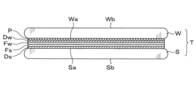
- FIG. 1 is a side view showing an example of the configuration of a polymerized wafer according to an embodiment.
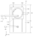
- 1 is a plan view schematically showing the configuration of a wafer processing system according to an embodiment.
- FIG. 1 is a plan view schematically showing the configuration of a laser irradiation device according to an embodiment.
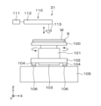
- FIG. 1 is a side view schematically showing the configuration of a laser irradiation device according to an embodiment.
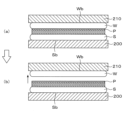
- FIG. 2 is a side view showing the operation of the separation device according to one embodiment.
- FIG. 2 is an explanatory diagram showing a state of a polymerized wafer irradiated with laser light.
- FIG. 2 is a flow diagram showing the main steps of wafer processing in the wafer processing system.
- FIG. 1 is a plan view schematically showing the configuration of a wafer processing system according to an embodiment.
- FIG. 1 is a plan view schematically showing the configuration of a wafer processing system according to an embodiment.
- FIG. 1 is a plan
- FIG. 3 is an explanatory diagram showing how heat generated in a polymerized wafer is diffused.
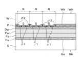
- FIG. 3 is an explanatory diagram showing how the first wafer expands due to laser light irradiation.
- FIG. 2 is an explanatory diagram showing a state of a polymerized wafer irradiated with laser light.
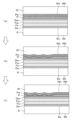
- FIG. 3 is an explanatory diagram showing how the first wafer and the laser absorption layer are peeled off.
- FIG. 3 is an explanatory diagram showing how the first wafer and the laser absorption layer are peeled off.
- FIG. 3 is an explanatory diagram showing a modified layer formed on the first substrate.
- FIG. 3 is an explanatory diagram showing a modified layer formed on the first substrate.
- FIG. 3 is an explanatory diagram showing how a peel-off promoting layer and a laser absorption layer are peeled off.
- FIG. 7 is a flow diagram showing main steps of wafer processing according to another embodiment.
- a device layer formed on the surface of a first wafer is transferred to a second wafer. is being carried out.
- the device layer is transferred to the second wafer by irradiating the laser absorption layer formed between the first wafer and the device layer with a laser beam to separate the first wafer and the laser absorption layer.
- Transfer of the device layer is performed, for example, by the method disclosed in Patent Document 1. That is, after locally heating the peeled oxide film (laser absorption layer) formed on the semiconductor substrate by irradiating the peeled oxide film with light (laser light), for example, the interface between the peeled oxide film and the semiconductor substrate is modified. A modified film is formed, and the semiconductor element is transferred to a transfer destination substrate by causing peeling using the modified film as a base point.
- the peeled oxide film laser absorption layer
- light laser light
- the inventors of the present invention conducted extensive research and came up with a new method for causing separation at the interface between the first wafer and the laser absorption layer. Specifically, instead of irradiating a laser absorption layer with a laser beam and causing the laser absorption layer to thermally expand and peel off, the laser absorption layer is irradiated with a laser beam and the heat generated thereby We have found a method in which the first wafer is expanded to cause separation at the interface between the first wafer and the laser absorption layer.
- the technology according to the present disclosure appropriately peels off the first substrate and the laser absorption layer in a polymerized substrate in which the laser absorption layer is formed at the interface between the first substrate and the second substrate.
- a wafer processing system as a substrate processing system and a wafer processing method as a substrate processing method according to the present embodiment will be described with reference to the drawings. Note that in this specification and the drawings, elements having substantially the same functional configuration are designated by the same reference numerals and redundant explanation will be omitted.
- a wafer processing system 1 processes a stacked wafer T, which is a stacked substrate in which a first wafer W and a second wafer S are bonded together, as shown in FIG.
- the first wafer W the surface to be joined to the second wafer S will be referred to as the front surface Wa
- the surface opposite to the front surface Wa will be referred to as the back surface Wb.
- the surface to be joined to the first wafer W is referred to as the front surface Sa
- the surface opposite to the front surface Sa is referred to as the back surface Sb.
- the first wafer W serving as the first substrate is, for example, a semiconductor wafer such as a silicon substrate.
- the first wafer W has a substantially disk shape.
- a laminated film in which a plurality of films are laminated is formed on the surface Wa of the first wafer W.
- the laminated film includes, in order from the surface Wa side, a laser absorption layer P, a device layer Dw, and a surface film Fw.
- the device layer Dw includes multiple devices. Examples of the surface film Fw include an oxide film (THOX film, SiO 2 film, TEOS film), SiC film, SiCN film, adhesive, and the like.
- the first wafer W is bonded to the second wafer S via this surface film Fw.
- the device layer Dw and the surface film Fw may not be formed on the surface Wa.
- the laser absorption layer P is formed on the second wafer S side, and a device layer Ds on the second wafer S side, which will be described later, is transferred to the first wafer W side.
- the laser absorption layer P absorbs the laser beam irradiated from the laser irradiation section 110 as described later.
- an oxide film SiO 2 film, TEOS film
- the laser absorption layer P is formed, for example, by a CVD (Chemical Vapor Deposition) process outside the wafer processing system 1, which will be described later.
- the composition of the oxide film (SiO 2 film, TEOS film) as the laser absorption layer P can be arbitrarily changed depending on the type and mixing ratio of the processing gas used in the CVD process. Note that details of the composition of the laser absorption layer P used in wafer processing according to the technology of the present disclosure will be described later.
- the second wafer S serving as the second substrate is, for example, a semiconductor wafer such as a silicon substrate.
- a laminated film is formed on the surface Sa of the second wafer S.
- the laminated film has a device layer Ds and a surface film Fs in this order from the surface Sa side.
- the device layer Ds and the surface film Fs are similar to the device layer Dw and the surface film Fw of the first wafer W, respectively.
- the surface film Fw of the first wafer W and the surface film Fs of the second wafer S are bonded. Note that the device layer Ds and the surface film Fs may not be formed on the surface Sa.
- the laminated film formed at the interface between the first wafer W and the second wafer S specifically, the laser absorption layer P, the device layers Dw, Ds, and the surface films Fw, Fs. It may also be referred to as an "interface layer.”
- the interface layer includes at least the laser absorption layer P.
- the type of laminated film formed at the interface between the first wafer W and the second wafer S is not limited to the example shown in FIG. 1.
- the laminated film may include a "peel-promoting film" to be described later for appropriately peeling the first wafer W and the laser absorption layer P.
- the above-mentioned interface layer includes a peel-off promoting film.
- the wafer processing system 1 has a configuration in which a loading/unloading block 10, a transport block 20, and a processing block 30 are integrally connected.
- the loading/unloading block 10 and the processing block 30 are provided around the transport block 20.
- the carry-in/out block 10 is arranged on the Y-axis negative direction side of the conveyance block 20.
- a laser irradiation device 31 (described later) and a separation device 32 (described later) of the processing block 30 are arranged on the X-axis negative direction side of the transport block 20, and a first cleaning device 33 (described later) and a second cleaning device 34 (described later) are located on the transport block 20. 20 in the positive direction of the X-axis.
- cassettes Ct, Cw, and Cs each capable of accommodating a plurality of stacked wafers T, a plurality of first wafers W, and a plurality of second wafers S are carried in and out of the carry-in/out block 10, respectively.
- the loading/unloading block 10 is provided with a cassette mounting table 11 .
- a plurality of cassettes for example, three cassettes Ct, Cw, and Cs, can be placed on the cassette mounting table 11 in a line in the X-axis direction. Note that the number of cassettes Ct, Cw, and Cs placed on the cassette mounting table 11 is not limited to this embodiment, and can be arbitrarily determined.
- the transport block 20 is provided with a wafer transport device 22 configured to be movable on a transport path 21 extending in the X-axis direction.
- the wafer transport device 22 has, for example, two transport arms 23, 23 that hold and transport the stacked wafer T, the first wafer W, or the second wafer S.
- Each transport arm 23 is configured to be movable in the horizontal direction, vertical direction, around the horizontal axis, and around the vertical axis. Note that the configuration of the transport arm 23 is not limited to this embodiment, and may have any configuration.
- the wafer transport device 22 then transfers the superposed wafers T, Cs, Ct, Cw, and Cs of the cassette mounting table 11, the laser irradiation device 31, the separation device 32, the first cleaning device 33, and the second cleaning device 34 to the cassettes Ct, Cw, and Cs on the cassette mounting table 11. It is configured to be able to transport a first wafer W and a second wafer S.
- the processing block 30 includes a laser irradiation device 31, a separation device 32, a first cleaning device 33, and a second cleaning device 34.
- the laser irradiation device 31 and the separation device 32 are stacked and arranged on the X-axis negative direction side of the transport block 20.
- the first cleaning device 33 and the second cleaning device 34 are stacked and arranged on the X-axis positive direction side of the transport block 20. Note that the number and arrangement of the laser irradiation device 31, the separation device 32, the first cleaning device 33, and the second cleaning device 34 are not limited to these.
- the laser irradiation device 31 irradiates the inside of the polymerized wafer T, more specifically, the laser absorption layer P formed on the front surface Wa of the first wafer W, with a laser beam, thereby irradiating the first wafer W and the laser absorption layer P. decreases the bonding strength at the interface.
- the interface in this embodiment, the interface between the first wafer W and the laser absorption layer P
- the bonding strength is reduced inside the polymerized wafer T may be referred to as a "separation surface" in the technology of the present disclosure.
- a delivery position A1 and a processing position A2 are set inside the laser irradiation device 31.
- the transfer position A1 is a position where the stacked wafer T can be transferred from the transport arm 23 to the chuck 100 described below, and a position where the stacked wafer T (laser absorption layer P) can be imaged by the camera 120 described below.
- the processing position A2 is a position where the polymerized wafer T (laser absorption layer P) can be irradiated with laser light from the laser irradiation unit 110, which will be described later.
- the laser irradiation device 31 has a chuck 100 as a substrate holding section that holds the overlapping wafer T on its upper surface.
- the chuck 100 has a holding surface for the stacked wafer T on its upper surface, and holds the entire back surface Sb of the second wafer S by suction or a part of the radially inner side of the back surface Sb.
- the chuck 100 is, for example, an electrostatic chuck (ESC) or a vacuum chuck.
- the chuck 100 is provided with a lifting pin (not shown) for supporting the stacked wafer T from below and lifting it up and down.
- the elevating pin is inserted into a through hole (not shown) formed through the chuck 100, and is configured to be able to rise and fall.
- the chuck 100 is supported by a slider table 102 via an air bearing 101.
- a rotation mechanism 103 is provided on the lower surface side of the slider table 102.
- the rotation mechanism 103 has a built-in motor as a drive source, for example.
- the chuck 100 is configured to be rotatable around the ⁇ axis (vertical axis) by a rotation mechanism 103 via an air bearing 101.
- the slider table 102 is movable between the above-mentioned delivery position A1 and processing position A2 by a moving mechanism 104 provided on the lower surface side of the slider table 102 along a rail 106 provided on the base 105 and extending in the Y-axis direction. It is configured.
- the driving source for the moving mechanism 104 is not particularly limited, but a linear motor may be used, for example.
- a laser irradiation unit 110 is provided above the chuck 100 at the processing position A2.
- the laser irradiation unit 110 includes a laser head 111, an optical system 112, and a lens 113.
- the laser irradiation unit 110 can scan a laser beam.
- scanning the laser beam means moving the laser beam irradiated from the lens 113 of the laser irradiation unit 110 with respect to the laser absorption layer P.
- the laser head 111 has a laser oscillator (not shown) that oscillates laser light in a pulsed manner.
- This laser light is a so-called pulsed laser.
- the laser beam is a CO 2 laser beam, and the wavelength of the CO 2 laser beam is, for example, 8.9 ⁇ m to 11 ⁇ m.
- the laser head 111 may include equipment other than the laser oscillator, such as an amplifier.
- the optical system 112 includes an optical element (not shown) that controls the intensity and position of the laser beam, an attenuator (not shown) that attenuates the laser beam and adjusts the output, and a laser scanning section (not shown) that scans the laser beam. (not shown).
- an optical element that controls the intensity and position of the laser beam
- an attenuator that attenuates the laser beam and adjusts the output
- a laser scanning section (not shown) that scans the laser beam. (not shown).
- a rotary wedge scanner or a galvano scanner is used as the laser scanning unit.
- the optical system 112 may be configured to be able to control branching of laser light.
- the lens 113 irradiates the polymerized wafer T held by the chuck 100 with laser light.
- the laser light emitted from the laser irradiation unit 110 passes through the first wafer W and is irradiated onto the laser absorption layer P.
- the lens 113 may be configured to be movable in the horizontal direction by a moving mechanism (not shown), or may be configured to be vertically movable by a lifting mechanism (not shown).
- a camera 120 is provided above the chuck 100 at the delivery position A1.
- the camera 120 includes one or more cameras selected from macro cameras, micro cameras, and the like. Note that the camera 120 may be configured to be movable in the horizontal direction by a moving mechanism (not shown), or may be configured to be vertically movable by a lifting mechanism (not shown).
- the camera 120 images the stacked wafer T held by the chuck 100.
- the camera 120 includes, for example, a coaxial lens, emits infrared light (IR), and receives reflected light from an object. Image data captured by the camera 120 is output to a control device 40, which will be described later.
- the separation device 32 as a separation unit separates the second wafer S (polymerized wafer T) from the interface between the first wafer W and the laser absorption layer P, which is the separation portion, and whose bonding strength has been reduced by the laser irradiation device 31.
- the first wafer W is peeled off from the substrate.
- the separation device 32 includes a suction chuck 200 that suction-holds the back surface Sb of the second wafer S from below, and a suction pad 210 that suction-holds the back surface Wb of the first wafer W from above. and has.
- the suction chuck 200 suction-holds the second wafer S
- the suction pad 210 suction-holds the first wafer W, and then raises the suction pad 210.
- the first wafer W is peeled off from the laser absorption layer P.
- the configuration of the separation device 32 is not limited to this, and can take any configuration as long as it can separate the first wafer W from the second wafer S.
- the first cleaning device 33 cleans the front surface Sa side of the second wafer S separated by peeling in the separation device 32. For example, a brush is brought into contact with the laser absorption layer P on the front surface Sa side of the second wafer S to clean the laser absorption layer P. Note that a pressurized cleaning liquid may be used to clean the second wafer S. Further, the first cleaning device 33 may have a configuration that cleans the back surface Sb of the second wafer S as well as the front surface Sa side.
- the second cleaning device 34 cleans the front surface Wa side of the first wafer W separated by peeling in the separation device 32. For example, a brush is brought into contact with the front surface Wa of the first wafer W to clean the front surface Wa. Note that a pressurized cleaning liquid may be used to clean the first wafer W. Further, the second cleaning device 34 may be configured to clean the front surface Wa side of the first wafer W as well as the back surface Wb.
- the first cleaning device 33 for cleaning the second wafer S and the second cleaning device 34 for cleaning the first wafer W are arranged independently.
- the cleaning of the first wafer W and the cleaning of the second wafer S may be performed using the same cleaning apparatus.
- the first wafer W and the second wafer S may be cleaned simultaneously or independently.
- the first wafer W is separated from the second wafer S using the separation device 32, but such separation may be performed inside the laser irradiation device 31.
- a transfer pad (not shown) that can be raised and lowered is provided at the delivery position A1 of the laser irradiation device 31. Then, with the chuck 100 suction-holding the second wafer S, the transfer pad suction-holds the first wafer W, and by further raising the transfer pad, the transfer from the second wafer S to the first wafer W is performed. Peel off.
- the above wafer processing system 1 is provided with a control device 40 as a control section.
- the control device 40 is, for example, a computer, and has a program storage section (not shown).
- the program storage unit stores a program for controlling the processing of the stacked wafers T in the wafer processing system 1.
- the program storage unit also stores programs for controlling the operations of drive systems such as the various processing devices and transport devices described above to realize wafer processing in the wafer processing system 1, which will be described later.
- the above program may be one that has been recorded on a computer-readable storage medium H, and may have been installed in the control device 40 from the storage medium H. Further, the storage medium H may be temporary or non-temporary.
- the first wafer W and the second wafer S are bonded in a bonding device (not shown) outside the wafer processing system 1 to form a superposed wafer T in advance.
- a cassette Ct containing a plurality of stacked wafers T is placed on the cassette mounting table 11 of the loading/unloading block 10.
- the superposed wafer T in the cassette Ct is taken out by the wafer transport device 22 and transported to the laser irradiation device 31.
- the stacked wafer T is transferred from the transfer arm 23 to a chuck 100 disposed at a transfer position A1, and the back surface Sb of the second wafer S is held by suction on the chuck 100.
- the moving mechanism 104 moves the chuck 100 to the processing position A2.
- the laser light L1 (CO 2 laser light) is irradiated from the laser irradiation unit 110 to the laser absorption layer P, more specifically, to the interface between the laser absorption layer P and the first wafer W in a pulsed manner. do.
- the laser beam L1 passes through the first wafer W from the back surface Wb side of the first wafer W and is absorbed in the laser absorption layer P. Then, the bonding strength between the laser absorption layer P and the first wafer W is reduced by this laser light L1.
- the bonding strength is reduced refers to a state in which the bonding strength is reduced at least compared to before irradiation with the laser beam L1
- the term “bonding strength is reduced” refers to a state in which the bonding strength is reduced at least compared to before irradiation with the laser beam L1 and the laser absorption layer P and the first wafer W are separated. including. Note that the mechanism of the decrease in bonding strength between the laser absorption layer P and the first wafer W caused by irradiation with the laser beam L1 will be described in detail later.
- the camera 120 When irradiating the laser light L1 to the laser absorption layer P at the processing position A2, first, the camera 120 images the superposed wafer T (first wafer W). Image data captured by camera 120 is output to control device 40 . The control device 40 determines the irradiation start position of the laser light L1 onto the laser absorption layer P based on the image data.
- the processing position A2 by irradiating the laser beam L1 in a pulsed manner while moving the laser irradiation unit 110 and the laser absorption layer P relatively, the entire surface of the laser absorption layer P is irradiated with the laser beam L1 in a plan view. However, the bonding force is reduced over the entire interface between the laser absorption layer P and the first wafer W.
- the laser beam L1 is irradiated in a pulsed manner while moving the laser beam L1 from the outside in the radial direction to the inside.
- the irradiation positions of the laser beam L1 on the radially outer annular region of the laser absorption layer P may be arranged spirally in plan view, or arranged annularly concentrically with the laser absorption layer P, for example. Good too.
- the method of irradiating the laser beam L1 at the processing position A2 is not necessarily limited to this, as long as the bonding force can be reduced over the entire interface between the laser absorption layer P and the first wafer W.
- the irradiation position of the laser beam L1 can be changed, for example. They may be arranged spirally or annularly concentrically with the laser absorption layer P in plan view.
- the chuck 100 (polymerized wafer T) is then moved by the moving mechanism 104. Move to delivery position A1.
- the stacked wafer T on the chuck 100 is transferred to the transfer arm 23 of the wafer transfer device 22 and transferred to the separation device 32.
- the separation device 32 as shown in FIG. 5(a), the back surface Sb of the second wafer S is held by suction with a suction chuck 200, and the back surface Wb of the first wafer W is further held by suction with a suction pad 210.
- the suction pad 210 is raised to separate the first wafer W from the laser absorption layer P. .
- the bonding strength at the interface between the laser absorption layer P and the first wafer W is reduced by the irradiation with the laser beam L1 as described above, the bonding strength is reduced from the laser absorption layer P to the first wafer W without applying a large load.
- the wafer W can be separated.
- the separated first wafer W is transferred from the suction pad 210 to the transfer arm 23 of the wafer transfer device 22, and then transferred to the second cleaning device 34.
- the first wafer W carried out from the separation device 32 is turned over, for example, by the operation of a reversing device (not shown) or the suction pad 210, so that the front surface Wa is facing upward. Thereafter, it may be transported to the second cleaning device 34.
- the surface Wa of the first wafer W which is the surface separated by the separation device 32, is cleaned.
- the second cleaning device 34 may clean the back surface Wb as well as the front surface Wa. Further, separate cleaning sections may be provided to clean the front surface Wa and the back surface Wb, respectively. Thereafter, the first wafer W that has been cleaned by the second cleaning device 34 is transferred to the cassette Cw of the cassette mounting table 11 by the wafer transfer device 22.
- the second wafer S held by the suction chuck 200 is transferred to the transfer arm 23 and transferred to the first cleaning device 33.
- the surface Sa side of the second wafer S which is the surface separated by the separation device 32, specifically, the surface of the laser absorption layer P is cleaned.
- the back surface Sb of the second wafer S may be cleaned together with the front surface of the laser absorption layer P. Further, cleaning sections for cleaning the front surface of the laser absorption layer P and the back surface Sb of the second wafer S may be provided separately. Thereafter, the second wafer S that has been cleaned by the first cleaning device 33 is transferred to the cassette Cs of the cassette mounting table 11 by the wafer transfer device 22.
- the polymerized wafer T held on the chuck 100 is irradiated with the laser light L1 from the back surface Wb side of the first wafer W (step St1).
- the laser beam L1 output from the lens 113 of the laser irradiation unit 110 passes through silicon (first wafer W) and is absorbed by the laser absorption layer P (step St2 in FIG. 7). ).
- the laser beam L1 absorbed by the laser absorption layer P is converted into heat according to its energy distribution (step St3 in FIG. 7).
- the temperature of the laser absorption layer P increases due to absorption of the laser beam L1.
- the temperature of the laser absorption layer P is highest in the area directly under the irradiation of the laser beam L1.
- most of the heat (Ht in the figure) generated in the laser absorption layer P due to absorption of the laser beam L1 is diffused toward the first wafer W (step St4 in FIG. 7). .
- thermal diffusion from the laser absorption layer P increases the temperature at the interface between the laser absorption layer P and the first wafer W (silicon).
- the influence of this heat causes the laser to emit light as shown in FIG.
- the first wafer W in the portion irradiated with the light L1 expands locally (plastically deforms in a downwardly convex shape with respect to the laser absorption layer P side) according to its temperature distribution (step St5 in FIG. 7).
- the area affected by the heat generated by the irradiation of the laser beam L1 may be referred to as the "irradiation area R" of the laser beam L1.
- the first wafer W locally expands in the irradiation area R of the laser beam L1.
- the entire surface of the laser absorption layer P in plan view is irradiated with the laser light L1.
- the entire surface of the laser absorption layer P is irradiated with the laser beam L1 multiple times at intervals.
- the first wafer W expands locally each time it is irradiated with the laser beam L1, that is, a plurality of irradiation regions R are formed at intervals in different parts in plan view.
- the laser absorption layer P is pressed from above (first wafer W side) due to the expansion of the first wafer W.
- a compressive stress ⁇ 1 is generated in the laser absorption layer P at the irradiation position of the laser beam L1.
- the generated compressive stress ⁇ 1 acts in the direction of peeling the first wafer W and the laser absorbing layer P (downward direction in the figure, toward the laser absorbing layer P side), causing the peeling.
- a stress ⁇ 2 is generated.
- the silicon (first wafer W) expands in the area directly under the irradiation of the laser beam L1 (the central part of the irradiation area R), and compressive stress ⁇ 1 is generated.
- a peeling stress ⁇ 2 which is a stress in the peeling direction caused by the compressive stress ⁇ 1, is generated at the end Re of the irradiation region R (see FIG. 9).
- This peeling stress ⁇ 2 is a tensile stress generated at the end Re of the irradiation region R.
- the generated compressive stress ⁇ 1 and peeling stress ⁇ 2 are accumulated inside the laser absorption layer P.
- the peeling stresses ⁇ 2 generated in the plurality of irradiation areas R act synergistically (redundantly).
- the processing position A2 of the laser irradiation device 31 As shown in FIG.
- the bonding strength is reduced on the entire surface of the first wafer W and the laser absorbing layer P.
- the first wafer W and the laser absorption layer P can be appropriately separated in the separation device 32 (step St7 in FIG. 7).
- the first wafer W in the central part of the irradiation area R (the area directly under the irradiation of the laser beam L1), even after peeling occurs at the end Re of the irradiation area R, the first wafer W In some cases, the laser absorption layer P is maintained in a connected state (not peeled off). Therefore, in the wafer processing system 1 according to the technology of the present disclosure, in order to reliably separate the first wafer W from the polymerized wafer T (laser absorption layer P) in the polymerized wafer T after irradiation with the laser beam L1, separation is performed. It is preferable to arrange a device 32 and provide a step of separating the first wafer W from the polymerized wafer T in the separation device 32.
- the above-mentioned ideal state is achieved, that is, separation from the laser absorption layer P occurs on the entire surface of the first wafer W. If the stacked wafers T are transferred to the separation device 32 in a state where the wafers T are separated, there is a risk that the first wafers W may fall from the second wafers S due to inertia or the like accompanying this transfer. Furthermore, if separation from the laser absorption layer P occurs over the entire surface of the first wafer W, even if there is no need to transport the polymerized wafer T after irradiation with the laser beam L1 to the separation device 32.
- the first wafer W is placed at the processing position A2.
- the irradiation conditions (irradiation position, output, etc.) of the laser beam L1 are controlled so that at least a part of the interface between the wafer W of No. 1 and the laser absorption layer P remains connected (not separated). It is preferable. This prevents the first wafer W from being completely separated from the laser absorption layer P and scattering or falling from the second wafer S during irradiation with the laser beam L1 or during transportation to the separation device 32, etc. Ru.
- the reduction in the bonding strength between the laser absorption layer P and the first wafer W at the processing position A2 of the laser irradiation device 31 is performed as described above. That is, in the present embodiment, the laser irradiation device 31 expands the first wafer W by heat generated by irradiation with the laser beam L1, and generates compressive stress ⁇ 1 in the laser absorption layer P, thereby causing the first wafer W and the laser beam to expand. A peeling stress ⁇ 2 is generated at the interface of the absorption layer P, which causes peeling at the interface between the laser absorption layer P and the first wafer W, thereby reducing the bonding strength.
- the laser absorption layer P is irradiated with the laser beam L1 a plurality of times as shown in FIG.
- the number of times the laser beam L1 is irradiated is not limited to a plurality of times until such peeling occurs.
- the peeling stress ⁇ 2 generated by a single irradiation (one time) of the laser beam L1 exceeds the adhesion force ⁇ , the single irradiation of the laser beam L1 will cause the first wafer to be removed at the end Re of the irradiation area R. Peeling may occur at the interface between W and the laser absorption layer P.
- the adhesion force ⁇ between the first wafer and the laser absorption layer is large, peeling cannot be caused appropriately at the interface between the laser absorption layer P and the first wafer W by irradiation with the laser beam L1. There is a risk. That is, when the adhesion force ⁇ between the first wafer and the laser absorption layer is large, the total amount of peeling stress ⁇ 2 accumulated inside the laser absorption layer P is There is a possibility that the adhesion force ⁇ between the two parts cannot be exceeded.
- the inventors conducted extensive studies and found that the adhesion force ⁇ , which is the threshold for peeling between the first wafer W and the laser absorbing layer P (peeling performance that is the "easiness of peeling"), has the following properties: It was found that the composition of the laser absorption layer P has an influence. In other words, the composition of the laser absorption layer P can be changed by controlling the type of processing gas, the mixing ratio, etc. in the formation process (for example, CVD process) of the laser absorption layer P performed outside the wafer processing system 1, for example. We have discovered the possibility of more appropriately and easily separating the laser absorption layer P and the first wafer W in the laser irradiation device 31 described above.
- the laser absorption layer P is a SiO 2 film as an oxide film
- the nitrogen (N) component ratio in the composition of the laser absorption layer P is high
- the first wafer W and the laser absorption layer P It was found that the adhesion force ⁇ of P decreased. This is because Si-O bonds and Si-N bonds mainly exist at the close contact interface between the first wafer W and the laser absorption layer P, and among these, the ratio of Si-N bonds with relatively low bonding strength is This is thought to be due to the increase in the price.
- the laser absorption layer P is a TEOS film as an oxide film
- the carbon (C) component ratio in the composition of the laser absorption layer P is high
- the first wafer W and the laser absorption layer P It was found that the adhesion force ⁇ of P decreased. This is because Si-O bonds and Si-C bonds mainly exist at the close contact interface between the first wafer W and the laser absorption layer P, and among these, the proportion of Si-C bonds with relatively low bonding strength is high. This is thought to be due to the fact that
- the nitrogen component ratio in the SiO 2 film as the laser absorption layer P can be improved, for example, by increasing the silane (SiH 4 ) ratio in the processing gas in the CVD process for forming the SiO 2 film. This is because by increasing the flow rate of silane in the processing gas, the flow rate of nitrous oxide (N 2 O) containing the oxygen (O) component in the processing gas for forming Si-O bonds decreases. This is due to this.
- the nitrogen component ratio in the laser absorption layer P is large (the laser absorption layer P is formed by increasing the silane flow rate), the nitrogen component ratio in the laser absorption layer P is small (the silane flow rate is decreased). It was found that the adhesion force ⁇ between the laser absorbing layer P and the first wafer W was weaker than in the case where the laser absorbing layer P was formed using the following methods.
- the present inventors investigated the case where the silane (SiH 4 ) flow rate during the formation of the laser absorption layer P was 15 ccm (example) and the case where the silane (SiH 4 ) flow rate during the formation of the laser absorption layer P was set to 15 ccm.
- a laser absorption layer P was formed with a thickness of 5 ccm (comparative example).
- XPS X-ray Photoelectron Spectroscopy
- a laser absorption layer analysis using a nanoindenter were performed for the laser absorption layer P formed under each condition.
- the adhesion force over the entire surface of P and the first wafer W was measured.
- the flow rate of nitrous oxide (N 2 O) during the formation of the laser absorption layer P was 400 ccm in both Examples and Comparative Examples.
- the film thickness of the laser absorption layer P to be formed was 1.0 ⁇ m in both Examples and Comparative Examples.
- the adhesion force between the laser absorption layer P and the first wafer W was measured using a nanoindenter, it was found that the adhesion force between the laser absorption layer P and the first wafer W was approximately 93 mN in the laser absorption layer P according to the example in which the nitrogen component ratio was large.
- the first wafer W could be separated, the laser absorption layer P and the first wafer W could not be separated in the laser absorption layer P according to the comparative example in which the nitrogen component ratio was small.
- the laser absorption layer P formed under the conditions of the example has a higher adhesion strength at the interface between the laser absorption layer P and the first wafer W than the laser absorption layer P formed under the conditions of the comparative example. was confirmed to be small. This is considered to be due to the high ratio of Si--N bonds with weak bonding strength at the interface between the first wafer W and the laser absorption layer P, as described above.
- the composition of the laser absorption layer P can be controlled by controlling the type and mixing ratio of the processing gas used when forming the laser absorption layer P. , it is possible to form a film having a weak adhesion force ⁇ , in other words, a film that easily peels off against the laser beam L1 in the laser irradiation device 31.
- a weak adhesion force ⁇ in other words, a film that easily peels off against the laser beam L1 in the laser irradiation device 31.
- a laser absorption layer P for absorbing laser light L1, a device layer Dw including a plurality of devices, and a surface film Fw for bonding with another substrate are formed on the surface of the first wafer W. do.
- These laser absorption layer P, device layer Dw, and surface film Fw may be collectively referred to as a "device structure" in the technology of the present disclosure.
- the composition of the laser absorption layer P formed on the surface of the first wafer W is determined based on the ease with which separation between the first wafer W and the laser absorption layer P occurs due to absorption of the laser beam L1. It is controlled according to the peeling performance. More specifically, the flow rate ratio of the processing gas during formation of the laser absorption layer P is controlled in accordance with the intended peeling performance between the first wafer W and the laser absorption layer P.
- the technology of the present disclosure can be said to have aspects related to the device structure formed on the surface of the first wafer W and aspects related to the manufacturing method of the device layer.
- the nitrogen component ratio of the laser absorption layer P is controlled as the composition of the laser absorption layer P.
- the carbon component ratio of the laser absorption layer P is controlled as the composition of the laser absorption layer P.
- the device layer Dw formed on the surface Wa of the first wafer W is transferred to the second wafer S in the wafer processing system 1, that is, the device layer Dw formed on the surface Wa of the first wafer W is transferred from the second wafer S to the first wafer
- the description has been given using the case where the entire surface of W is separated the technology according to the present disclosure can also be applied to the case where a part of the first wafer W is separated from the second wafer S.
- a peripheral edge removing device (not shown) for removing the peripheral edge We of the first wafer W is arranged in the processing block 30 of the wafer processing system 1 instead of the separating device 32.
- a peripheral edge modified layer M1 is formed along the boundary between the peripheral edge part We and the central part Wc of the first wafer W to be removed, and a laser beam L2 is emitted from the peripheral edge modified layer M1 toward the outside in the radial direction. irradiation to form divided modified layers M2. Note that in the subsequent drawings, illustration of the divided modified layer M2 formed inside the first wafer W is omitted for clarity of illustration.
- the peripheral modified layer M1 and the divided modified layer M2 are formed inside the first wafer W, next, in the same laser irradiation device 31, the peripheral modified layer M1 and the divided modified layer M2 are formed at least in a region corresponding to the peripheral part We to be removed.
- the laser absorption layer P is irradiated with a laser beam L1 (for example, a CO 2 laser) to reduce the bonding strength at the interface between the first wafer W and the laser absorption layer P, as shown in FIG. 13(b).
- a laser beam L1 for example, a CO 2 laser
- the overlapping wafer T whose bonding strength in the region corresponding to the peripheral edge We has been reduced is then transported to a peripheral edge removal device (not shown), and is separated into a first wafer W and a second wafer S as shown in FIG. 13(c).
- the peripheral edge We of the first wafer W is removed by inserting, for example, a wedge-shaped insertion member 300 toward the interface with the first wafer W. More specifically, the peripheral edge We of the first wafer W is separated from the second wafer S using the peripheral modified layer M1 as a base, and the peripheral edge We is divided into small pieces using the divided modified layer M2 as a base.
- the peripheral edge We of the first wafer W is separated from the second wafer S in this way, the first wafer W and By reducing the bonding strength at the interface of the laser absorption layer P, the peripheral edge We can be appropriately removed. Furthermore, at this time, the adhesion between the first wafer W and the laser absorption layer P is reduced by controlling the composition of the oxide film constituting the laser absorption layer P as described above, at least in the region corresponding to the peripheral edge We. In this way, the peripheral edge portion We can be removed more appropriately.
- the first wafer W and the first wafer W are separated, such as the entire surface separation of the first wafer W shown in FIGS. 8 to 12 and the edge trim processing of the first wafer W shown in FIG. Peeling occurred at the interface of the laser absorption layer P.
- a peel-promoting film may be formed on the surface Wa of the first wafer W to appropriately peel the first wafer W and the laser absorption layer P; Peeling may occur at the interface between the film and the laser absorption layer P.
- a peeling promoting film Pe on the surface Wa of the first wafer W, a peeling promoting film Pe, a laser absorption layer P, a device layer Dw, and a surface film Fw as a laminated film are formed in this order. It can be formed by laminating.
- the peeling promoting film Pe is formed to facilitate peeling of the first wafer W from the second wafer S, and its adhesion with the first wafer W (silicon) is higher than that with the laser absorption layer P. It is made of a material that is lower in transparency than the laser beam L1 and is transparent to the laser beam L1, for example, silicon nitride (SiN).
- the laser absorption layer P is irradiated with the laser light L1 (step Sp1 in FIG. 16).
- the laser beam L1 passes through the first wafer W and the peeling promoting film Pe, and is absorbed by the laser absorption layer P (step Sp2 in FIG. 16).
- the laser light L1 absorbed by the laser absorption layer P is converted into heat according to its energy distribution (step Sp3 in FIG. 16), thereby increasing the temperature of the laser absorption layer P.
- Most of the heat generated in the laser absorption layer P due to the absorption of the laser beam L1 is diffused to the peeling promoting film Pe on the first wafer W side (step Sp4 in FIG. 16), and this thermal diffusion causes the laser absorption
- the temperature at the interface between the layer P and the peel promoting film Pe increases.
- the influence of this heat causes a phenomenon as shown in FIG. 15(b).
- the peeling promoting film Pe expands locally according to its temperature distribution (step Sp5 in FIG. 16).
- the thermal influence at the interface between the laser absorption layer P and the peeling promoting film Pe may affect the first wafer W, and as shown in FIG. 15(b), the first wafer W also responds to the temperature distribution. It may also expand locally.
- the peel-promoting film Pe (and the first wafer W) expands locally, the stress generated by this expansion causes the laser-absorbing layer P with low adhesion to the peel-promoting film as shown in FIG. 15(c). Peeling occurs at the interface of Pe, and as a result, the bonding strength between the laser absorption layer P and the peeling promoting film Pe decreases (step Sp6 in FIG. 16). Then, by connecting the peeling over the entire surface of the interface between the peeling promoting film Pe and the laser absorbing layer P, the bonding strength is reduced over the entire surface of the peeling promoting film Pe and the laser absorbing layer P, and thereby the separating device 32 promotes peeling. The film Pe and the laser absorption layer P (first wafer W and second wafer S) can be appropriately separated (step Sp7 in FIG. 16).
- the peeling promoting film Pe is formed on the surface Wa of the first wafer W, and the adhesion with the first wafer W (silicon) is lower than the adhesion with the laser absorption layer P. Expanding the peeling promoting film Pe instead of the wafer W or together with the first wafer W can also transfer the device layer Dw formed on the surface Wa of the first wafer W and edge trim of the first wafer W. Processes can be executed appropriately.
- the peel-off promoting film Pe was formed at the interface between the first wafer W and the laser absorption layer P, but it is also possible to form the peel-off promoting film Pe at the interface between the laser absorbing layer P and the device layer Dw, for example. However, by causing peeling at the interface between the laser absorption layer P and the peeling promoting film Pe, the peeling promoting film Pe may be left on the second wafer S side to which the device layer Dw is transferred.
- Wafer processing system 32 Separation device 40 Control device 100
- Chuck 110 Laser irradiation section L1 Laser light
- Laser absorption layer R Irradiation area
- Second wafer T Polymerized wafer W
Landscapes
- Engineering & Computer Science (AREA)
- Physics & Mathematics (AREA)
- Optics & Photonics (AREA)
- Plasma & Fusion (AREA)
- Mechanical Engineering (AREA)
- Chemical & Material Sciences (AREA)
- Chemical Kinetics & Catalysis (AREA)
- General Chemical & Material Sciences (AREA)
- Oil, Petroleum & Natural Gas (AREA)
- Container, Conveyance, Adherence, Positioning, Of Wafer (AREA)
- Element Separation (AREA)
Priority Applications (1)
| Application Number | Priority Date | Filing Date | Title |
|---|---|---|---|
| JP2024536783A JP7815447B2 (ja) | 2022-07-27 | 2023-04-25 | 基板処理システム、基板処理方法及びデバイス構造 |
Applications Claiming Priority (2)
| Application Number | Priority Date | Filing Date | Title |
|---|---|---|---|
| JP2022-119975 | 2022-07-27 | ||
| JP2022119975 | 2022-07-27 |
Publications (1)
| Publication Number | Publication Date |
|---|---|
| WO2024024191A1 true WO2024024191A1 (ja) | 2024-02-01 |
Family
ID=89705935
Family Applications (1)
| Application Number | Title | Priority Date | Filing Date |
|---|---|---|---|
| PCT/JP2023/016356 Ceased WO2024024191A1 (ja) | 2022-07-27 | 2023-04-25 | 基板処理システム、基板処理方法及びデバイス構造 |
Country Status (3)
| Country | Link |
|---|---|
| JP (1) | JP7815447B2 (https=) |
| TW (1) | TW202405883A (https=) |
| WO (1) | WO2024024191A1 (https=) |
Citations (4)
| Publication number | Priority date | Publication date | Assignee | Title |
|---|---|---|---|---|
| JP2007220749A (ja) * | 2006-02-14 | 2007-08-30 | Seiko Epson Corp | 半導体装置の製造方法 |
| WO2021192853A1 (ja) * | 2020-03-24 | 2021-09-30 | 東京エレクトロン株式会社 | 基板処理方法及び基板処理装置 |
| WO2021192854A1 (ja) * | 2020-03-24 | 2021-09-30 | 東京エレクトロン株式会社 | 基板処理方法及び基板処理装置 |
| JP2022091504A (ja) * | 2020-12-09 | 2022-06-21 | 東京エレクトロン株式会社 | レーザ照射システム、基板処理装置及び基板処理方法 |
-
2023
- 2023-04-25 JP JP2024536783A patent/JP7815447B2/ja active Active
- 2023-04-25 WO PCT/JP2023/016356 patent/WO2024024191A1/ja not_active Ceased
- 2023-06-01 TW TW112120516A patent/TW202405883A/zh unknown
Patent Citations (4)
| Publication number | Priority date | Publication date | Assignee | Title |
|---|---|---|---|---|
| JP2007220749A (ja) * | 2006-02-14 | 2007-08-30 | Seiko Epson Corp | 半導体装置の製造方法 |
| WO2021192853A1 (ja) * | 2020-03-24 | 2021-09-30 | 東京エレクトロン株式会社 | 基板処理方法及び基板処理装置 |
| WO2021192854A1 (ja) * | 2020-03-24 | 2021-09-30 | 東京エレクトロン株式会社 | 基板処理方法及び基板処理装置 |
| JP2022091504A (ja) * | 2020-12-09 | 2022-06-21 | 東京エレクトロン株式会社 | レーザ照射システム、基板処理装置及び基板処理方法 |
Also Published As
| Publication number | Publication date |
|---|---|
| JPWO2024024191A1 (https=) | 2024-02-01 |
| JP7815447B2 (ja) | 2026-02-17 |
| TW202405883A (zh) | 2024-02-01 |
Similar Documents
| Publication | Publication Date | Title |
|---|---|---|
| JP7304433B2 (ja) | 基板処理方法及び基板処理装置 | |
| JP7809180B2 (ja) | 基板処理方法、基板処理装置、プログラム及びコンピュータ記憶媒体 | |
| JP7499845B2 (ja) | 基板処理方法及び基板処理装置 | |
| JP7386077B2 (ja) | 基板処理装置及び基板処理方法 | |
| JP7354420B2 (ja) | 基板処理方法及び基板処理装置 | |
| JP2025105952A (ja) | 処理方法及び処理システム | |
| WO2022153886A1 (ja) | 基板処理装置、基板処理方法及び基板製造方法 | |
| WO2022153894A1 (ja) | 基板処理装置及び基板処理方法 | |
| WO2024024191A1 (ja) | 基板処理システム、基板処理方法及びデバイス構造 | |
| WO2022153895A1 (ja) | 基板処理装置及び基板処理方法 | |
| CN114830293A (zh) | 基板处理装置和基板处理方法 | |
| JP7814972B2 (ja) | 重合基板の処理方法及び基板処理システム | |
| JP7808697B2 (ja) | 基板処理装置及び基板処理方法 | |
| WO2024247740A1 (ja) | 基板処理方法及び基板処理システム | |
| CN121219097A (zh) | 基板处理方法和基板处理装置 |
Legal Events
| Date | Code | Title | Description |
|---|---|---|---|
| 121 | Ep: the epo has been informed by wipo that ep was designated in this application |
Ref document number: 23845931 Country of ref document: EP Kind code of ref document: A1 |
|
| WWE | Wipo information: entry into national phase |
Ref document number: 2024536783 Country of ref document: JP |
|
| NENP | Non-entry into the national phase |
Ref country code: DE |
|
| 122 | Ep: pct application non-entry in european phase |
Ref document number: 23845931 Country of ref document: EP Kind code of ref document: A1 |