WO2024023877A1 - プラズマ処理方法 - Google Patents
プラズマ処理方法 Download PDFInfo
- Publication number
- WO2024023877A1 WO2024023877A1 PCT/JP2022/028584 JP2022028584W WO2024023877A1 WO 2024023877 A1 WO2024023877 A1 WO 2024023877A1 JP 2022028584 W JP2022028584 W JP 2022028584W WO 2024023877 A1 WO2024023877 A1 WO 2024023877A1
- Authority
- WO
- WIPO (PCT)
- Prior art keywords
- pulse
- plasma
- processing method
- plasma processing
- frequency
- Prior art date
- Legal status (The legal status is an assumption and is not a legal conclusion. Google has not performed a legal analysis and makes no representation as to the accuracy of the status listed.)
- Ceased
Links
Images




Classifications
-
- H—ELECTRICITY
- H01—ELECTRIC ELEMENTS
- H01J—ELECTRIC DISCHARGE TUBES OR DISCHARGE LAMPS
- H01J37/00—Discharge tubes with provision for introducing objects or material to be exposed to the discharge, e.g. for the purpose of examination or processing thereof
- H01J37/32—Gas-filled discharge tubes
- H01J37/32009—Arrangements for generation of plasma specially adapted for examination or treatment of objects, e.g. plasma sources
- H01J37/32082—Radio frequency generated discharge
- H01J37/32137—Radio frequency generated discharge controlling of the discharge by modulation of energy
- H01J37/32146—Amplitude modulation, includes pulsing
-
- H—ELECTRICITY
- H01—ELECTRIC ELEMENTS
- H01J—ELECTRIC DISCHARGE TUBES OR DISCHARGE LAMPS
- H01J37/00—Discharge tubes with provision for introducing objects or material to be exposed to the discharge, e.g. for the purpose of examination or processing thereof
- H01J37/32—Gas-filled discharge tubes
- H01J37/32009—Arrangements for generation of plasma specially adapted for examination or treatment of objects, e.g. plasma sources
- H01J37/32192—Microwave generated discharge
-
- H—ELECTRICITY
- H01—ELECTRIC ELEMENTS
- H01J—ELECTRIC DISCHARGE TUBES OR DISCHARGE LAMPS
- H01J37/00—Discharge tubes with provision for introducing objects or material to be exposed to the discharge, e.g. for the purpose of examination or processing thereof
- H01J37/32—Gas-filled discharge tubes
- H01J37/32009—Arrangements for generation of plasma specially adapted for examination or treatment of objects, e.g. plasma sources
- H01J37/32192—Microwave generated discharge
- H01J37/32302—Plural frequencies
-
- H—ELECTRICITY
- H10—SEMICONDUCTOR DEVICES; ELECTRIC SOLID-STATE DEVICES NOT OTHERWISE PROVIDED FOR
- H10P—GENERIC PROCESSES OR APPARATUS FOR THE MANUFACTURE OR TREATMENT OF DEVICES COVERED BY CLASS H10
- H10P50/00—Etching of wafers, substrates or parts of devices
- H10P50/20—Dry etching; Plasma etching; Reactive-ion etching
- H10P50/24—Dry etching; Plasma etching; Reactive-ion etching of semiconductor materials
- H10P50/242—Dry etching; Plasma etching; Reactive-ion etching of semiconductor materials of Group IV materials
-
- H—ELECTRICITY
- H10—SEMICONDUCTOR DEVICES; ELECTRIC SOLID-STATE DEVICES NOT OTHERWISE PROVIDED FOR
- H10P—GENERIC PROCESSES OR APPARATUS FOR THE MANUFACTURE OR TREATMENT OF DEVICES COVERED BY CLASS H10
- H10P50/00—Etching of wafers, substrates or parts of devices
- H10P50/20—Dry etching; Plasma etching; Reactive-ion etching
- H10P50/26—Dry etching; Plasma etching; Reactive-ion etching of conductive or resistive materials
- H10P50/264—Dry etching; Plasma etching; Reactive-ion etching of conductive or resistive materials by chemical means
- H10P50/266—Dry etching; Plasma etching; Reactive-ion etching of conductive or resistive materials by chemical means by vapour etching only
- H10P50/267—Dry etching; Plasma etching; Reactive-ion etching of conductive or resistive materials by chemical means by vapour etching only using plasmas
- H10P50/268—Dry etching; Plasma etching; Reactive-ion etching of conductive or resistive materials by chemical means by vapour etching only using plasmas of silicon-containing layers
-
- H—ELECTRICITY
- H10—SEMICONDUCTOR DEVICES; ELECTRIC SOLID-STATE DEVICES NOT OTHERWISE PROVIDED FOR
- H10P—GENERIC PROCESSES OR APPARATUS FOR THE MANUFACTURE OR TREATMENT OF DEVICES COVERED BY CLASS H10
- H10P50/00—Etching of wafers, substrates or parts of devices
- H10P50/20—Dry etching; Plasma etching; Reactive-ion etching
- H10P50/28—Dry etching; Plasma etching; Reactive-ion etching of insulating materials
- H10P50/282—Dry etching; Plasma etching; Reactive-ion etching of insulating materials of inorganic materials
- H10P50/283—Dry etching; Plasma etching; Reactive-ion etching of insulating materials of inorganic materials by chemical means
-
- H—ELECTRICITY
- H10—SEMICONDUCTOR DEVICES; ELECTRIC SOLID-STATE DEVICES NOT OTHERWISE PROVIDED FOR
- H10P—GENERIC PROCESSES OR APPARATUS FOR THE MANUFACTURE OR TREATMENT OF DEVICES COVERED BY CLASS H10
- H10P50/00—Etching of wafers, substrates or parts of devices
- H10P50/69—Etching of wafers, substrates or parts of devices using masks for semiconductor materials
- H10P50/691—Etching of wafers, substrates or parts of devices using masks for semiconductor materials for Group V materials or Group III-V materials
- H10P50/692—Etching of wafers, substrates or parts of devices using masks for semiconductor materials for Group V materials or Group III-V materials characterised by their composition, e.g. multilayer masks or materials
-
- H—ELECTRICITY
- H10—SEMICONDUCTOR DEVICES; ELECTRIC SOLID-STATE DEVICES NOT OTHERWISE PROVIDED FOR
- H10P—GENERIC PROCESSES OR APPARATUS FOR THE MANUFACTURE OR TREATMENT OF DEVICES COVERED BY CLASS H10
- H10P50/00—Etching of wafers, substrates or parts of devices
- H10P50/69—Etching of wafers, substrates or parts of devices using masks for semiconductor materials
- H10P50/691—Etching of wafers, substrates or parts of devices using masks for semiconductor materials for Group V materials or Group III-V materials
- H10P50/693—Etching of wafers, substrates or parts of devices using masks for semiconductor materials for Group V materials or Group III-V materials characterised by their size, orientation, disposition, behaviour or shape, in horizontal or vertical plane
- H10P50/695—Etching of wafers, substrates or parts of devices using masks for semiconductor materials for Group V materials or Group III-V materials characterised by their size, orientation, disposition, behaviour or shape, in horizontal or vertical plane characterised by the process involved to create the mask, e.g. lift-off masks or sidewalls or to modify the mask
-
- H—ELECTRICITY
- H10—SEMICONDUCTOR DEVICES; ELECTRIC SOLID-STATE DEVICES NOT OTHERWISE PROVIDED FOR
- H10W—GENERIC PACKAGES, INTERCONNECTIONS, CONNECTORS OR OTHER CONSTRUCTIONAL DETAILS OF DEVICES COVERED BY CLASS H10
- H10W10/00—Isolation regions in semiconductor bodies between components of integrated devices
-
- H—ELECTRICITY
- H10—SEMICONDUCTOR DEVICES; ELECTRIC SOLID-STATE DEVICES NOT OTHERWISE PROVIDED FOR
- H10W—GENERIC PACKAGES, INTERCONNECTIONS, CONNECTORS OR OTHER CONSTRUCTIONAL DETAILS OF DEVICES COVERED BY CLASS H10
- H10W10/00—Isolation regions in semiconductor bodies between components of integrated devices
- H10W10/01—Manufacture or treatment
-
- H—ELECTRICITY
- H10—SEMICONDUCTOR DEVICES; ELECTRIC SOLID-STATE DEVICES NOT OTHERWISE PROVIDED FOR
- H10W—GENERIC PACKAGES, INTERCONNECTIONS, CONNECTORS OR OTHER CONSTRUCTIONAL DETAILS OF DEVICES COVERED BY CLASS H10
- H10W10/00—Isolation regions in semiconductor bodies between components of integrated devices
- H10W10/01—Manufacture or treatment
- H10W10/011—Manufacture or treatment of isolation regions comprising dielectric materials
- H10W10/014—Manufacture or treatment of isolation regions comprising dielectric materials using trench refilling with dielectric materials, e.g. shallow trench isolations
-
- H—ELECTRICITY
- H10—SEMICONDUCTOR DEVICES; ELECTRIC SOLID-STATE DEVICES NOT OTHERWISE PROVIDED FOR
- H10W—GENERIC PACKAGES, INTERCONNECTIONS, CONNECTORS OR OTHER CONSTRUCTIONAL DETAILS OF DEVICES COVERED BY CLASS H10
- H10W10/00—Isolation regions in semiconductor bodies between components of integrated devices
- H10W10/10—Isolation regions comprising dielectric materials
- H10W10/17—Isolation regions comprising dielectric materials formed using trench refilling with dielectric materials, e.g. shallow trench isolations
-
- H—ELECTRICITY
- H01—ELECTRIC ELEMENTS
- H01J—ELECTRIC DISCHARGE TUBES OR DISCHARGE LAMPS
- H01J2237/00—Discharge tubes exposing object to beam, e.g. for analysis treatment, etching, imaging
- H01J2237/32—Processing objects by plasma generation
- H01J2237/33—Processing objects by plasma generation characterised by the type of processing
- H01J2237/332—Coating
-
- H—ELECTRICITY
- H01—ELECTRIC ELEMENTS
- H01J—ELECTRIC DISCHARGE TUBES OR DISCHARGE LAMPS
- H01J2237/00—Discharge tubes exposing object to beam, e.g. for analysis treatment, etching, imaging
- H01J2237/32—Processing objects by plasma generation
- H01J2237/33—Processing objects by plasma generation characterised by the type of processing
- H01J2237/334—Etching
Definitions
- the present invention relates to a plasma processing method.
- Fin Field Effect Transistors hereinafter also referred to as "Fin-FETs”
- Fin-FETs Fin Field Effect Transistors
- GAA Gate-All-Around
- semiconductor devices continue to become smaller and have higher aspect ratios, it is expected that patterns with more complex shapes will be formed. It is required to establish a vertical machining process with high selectivity corresponding to the structure.
- STI Fin-FET shallow trench isolation
- One of the techniques for realizing highly accurate plasma etching is a plasma etching method using a pulsed power source.
- the density and composition of radicals generated by decomposition of a reactive gas by plasma are measured.
- the density and composition of the radicals are controlled by pulse modulating the power of the plasma generator at a constant cycle and controlling the duty ratio of the pulse modulation based on the measurement results.
- Patent Document 2 high power power and low power power are alternately supplied to a high frequency coil (antenna coil) for plasma generation, and a protective film is formed by sputtering when the high power is used, and when the low power is used, a protective film is formed by sputtering.
- a method is disclosed in which a via with a high aspect ratio is formed in a silicon substrate by performing an etching process and alternately repeating an etching process and a protective film forming process.
- the high frequency RF bias power causes local charging, and the side surfaces of the hard mask material and the silicon substrate become negatively charged. For this reason, the trajectory of ions is bent, and the number of ions incident on the side surfaces of the silicon substrate increases, resulting in a phenomenon called side etching in which etching progresses laterally.
- the problem of loss of verticality of etching is not taken into account.
- An object of the present invention is to provide a technique that can realize vertical etching by controlling process conditions.
- one of the typical plasma processing methods of the present invention is a plasma processing method for forming shallow trench isolation, which includes a first step of etching silicon with plasma, and a step of etching silicon containing silicon element. a second step of depositing a deposited film containing SiO on the mask; a third step of etching the silicon with plasma so that the etched shape is vertical; and a fourth step of depositing a deposited film containing SiO on the mask.
- the first step to the fourth step are repeated a predetermined number of times, the plasma in the third step is generated by high frequency power modulated by the first pulse, and the plasma in the third step is The step is performed while supplying high frequency power modulated by a second pulse to the sample having silicon as a substrate, and the frequency of the first pulse in the third step is equal to the frequency of the first pulse in the third step.
- the frequency of the second pulse is higher than that of the second pulse.
- FIG. 1 is a diagram showing a plasma processing apparatus in which a plasma processing method according to a first embodiment of the present invention is implemented.
- FIG. 2 is a schematic diagram showing how the plasma processing method according to the first embodiment is performed.
- FIG. 3 is a diagram showing the relationship between pulse frequency and undercut amount when plasma generation power is pulse-modulated.
- FIG. 4 is a diagram showing the relationship between pulse frequency and undercut amount when bias power is pulse modulated.
- FIG. 5 is a diagram schematically showing the relationship between the bias power and the saturated ion current on the wafer, obtained in the first embodiment.
- FIG. 6 is a diagram schematically showing the relationship between plasma generation power and plasma density when the duty ratio is 40% and the pulse frequency is 1300 Hz.
- FIG. 7 is a diagram schematically showing the relationship between plasma generation power and plasma density when the duty ratio is 40% and the pulse frequency is 1100 Hz.
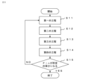
- FIG. 8 is a diagram showing a flowchart of a method for forming an STI.
- FIG. 9 is a diagram schematically showing a part of the silicon substrate before the STI formation process is performed.
- FIG. 10 is a diagram schematically showing a part of the silicon substrate when the first step is performed.
- FIG. 11 is a diagram schematically showing a part of the silicon substrate when the second step is performed.
- FIG. 12 is a diagram schematically showing a part of the silicon substrate when the third step is performed.
- FIG. 13 is a diagram schematically showing a part of the silicon substrate when the fourth step is performed.
- FIG. 14 is a diagram schematically showing a part of the silicon substrate when the first to fourth steps are repeated and the trench is etched to a predetermined depth.
- FIG. 15 is a diagram schematically showing how the first to fourth steps are repeated.
- FIG. 16 is a diagram schematically showing a part of a silicon substrate in an etching process as a comparative example.
- pulse modulation (hereinafter also referred to as “pulse modulation”) is to turn on when there is an output, turn off when there is no output, and repeat on and off at a predetermined frequency.
- the predetermined frequency is also referred to as a "pulse frequency,””pulsefrequency,” or “repetition frequency.”
- the duty ratio is the sum of the on period and the off period, that is, the ratio of the on period to one cycle of repetition.
- Shallow Trench Isolation refers to a trench for element isolation formed by etching a silicon substrate or the like.
- FIG. 1 is a diagram showing a plasma processing apparatus in which a plasma processing method according to a first embodiment of the present invention is implemented.
- the plasma processing apparatus 100 includes a vacuum processing chamber 101 in which plasma processing is performed.
- a lower electrode 103 is provided inside the vacuum processing chamber 101, and the lower electrode 103 is provided with a wafer mounting surface for holding the wafer 102.
- the microwave transmission window 104 is made of a material such as quartz that transmits microwaves while keeping the inside of the vacuum processing chamber 101 airtight.
- Microwaves generated from a magnetron (hereinafter also referred to as “plasma generator”) 106 pass through a microwave transmission window 104 through a waveguide 105 and propagate into the vacuum processing chamber 101 .
- the solenoid coil 107 is provided around the vacuum processing chamber 101 and generates a magnetic field within the vacuum processing chamber 101.
- a voltage is applied to the lower electrode 103 from a connected electrostatic adsorption power supply 108, and an electrostatic force is generated between the wafer 102 and the wafer mounting surface. The generated electrostatic force fixes the wafer 102 to the wafer mounting surface.
- a magnetron drive power source (hereinafter also referred to as “plasma generation power source”) 113 supplies high frequency power (hereinafter also referred to as “plasma generation power”) for generating plasma to the magnetron 106.
- the plasma generation power is also referred to as high frequency power modulated by the first pulse.
- the substrate bias power supply 109 supplies the lower electrode 103 with bias power that is supplied to the substrate that is the sample. Bias power is also referred to as high frequency power modulated by the second pulse.
- the magnetron drive power supply 113 and the substrate bias power supply 109 are controlled by a power control section 114.
- the wafer loading port 110 is an opening for loading the wafer 102 into or out of the vacuum processing chamber 101.
- the gas supply port 111 is an opening through which gas supplied to the vacuum processing chamber 101 is conducted.
- the plasma processing apparatus 100 is also provided with a vacuum exhaust device.
- the vacuum evacuation device has a function of reducing the pressure in the vacuum processing chamber 101 to a desired pressure and evacuating reaction products generated during the plasma processing process from the vacuum processing chamber 101.
- the plasma processing apparatus 100 performs a plasma processing method in which a sample is subjected to plasma processing using high frequency power for generating plasma and bias power for applying a bias to the sample.
- etching gas is supplied into the vacuum processing chamber 101 from the gas supply port 111, and the pressure inside the vacuum processing chamber 101 is adjusted to a desired pressure.
- the wafer 102 is electrostatically attracted to the wafer mounting surface above the lower electrode 103 by applying a DC voltage of several hundred volts using the electrostatic adsorption power supply 108 .
- the magnetron 106 oscillates microwaves with a frequency of 2.45 GHz. This microwave is propagated into the vacuum processing chamber 101 through the waveguide 105.
- the magnetron 106 does not oscillate microwaves.
- a magnetic field is generated within the vacuum processing chamber 101 by a solenoid coil 107, and high-density plasma 112 is generated within the vacuum processing chamber 101 due to the interaction of this magnetic field and the oscillated microwaves.
- bias power is supplied from the substrate bias power supply 109 to the lower electrode 103.
- the energy with which ions in the plasma enter the wafer is controlled, and the etching process of the wafer 102 is controlled.
- pulsed plasma is generated by pulse modulating the plasma generation power supplied to the magnetron 106.
- Pulsed plasma controls the dissociation of plasma by repeating the on-state and off-state where plasma generation power is output, thereby controlling the dissociation state of radicals and ion density.
- the pulse frequency and duty ratio for pulse-modulated plasma are control parameters. Plasma generated by these control parameters is also called pulsed plasma.
- the output of the substrate bias power supply 109 is also pulse-modulated, so that the pulse frequency and duty ratio can be controlled, and pulse-modulated bias power can be applied to the lower electrode 103.
- the plasma generation power or bias power is controlled by a power control section 114.
- the duty ratio of the plasma generation power can be changed as appropriate within the range of 10% to 90% according to the specification conditions of the plasma processing apparatus 100, and the duty ratio of the bias power can be changed within the range of 2% to 90%. It can be changed as appropriate. Normally, the bias power is controlled to be turned on only when the plasma generation power is turned on.
- the pulse frequency of the plasma generation power can be changed as appropriate within the range of 100 Hz to 2000 Hz
- the pulse frequency of the bias power can be changed as appropriate within the range of 100 Hz to 2000 Hz.
- FIG. 2 is a schematic diagram showing how the plasma processing method according to the first embodiment is performed.
- FIG. 2A is a diagram schematically showing a part of a cross section of the silicon substrate 201 before plasma processing.
- the initial structure of the silicon substrate 201 is such that a mask 202 is formed on the silicon substrate 201.
- the mask 202 is formed with a pattern having gaps at predetermined intervals, and the interval w1 between the gaps between adjacent masks 202 is 20 nm or less, for example, about 10 nm when used in the STI forming process.
- the silicon substrate 201 is etched to a depth of about 130 nm, forming a trench with an aspect ratio of about 6.5.
- the mask 202 is assumed to be a hard mask, but the type of mask is not limited to this.
- FIG. 2(b) is a diagram showing the progress of etching of the silicon substrate 201.
- a portion of the silicon substrate 201 defined by the gap between the masks 202 is etched to form a trench tr.
- the processing conditions for example, a mixed gas containing halogen gas is used, and the pressure is 0.5 Pa or less.
- FIG. 2(c) is a diagram showing how the etching of the silicon substrate 201 has further progressed.
- a region r1 of trench tr is etched in a direction parallel to the main surface of silicon substrate 201, creating a neck shape.
- the occurrence of such a neck shape is called an undercut.
- the undercut amount can be evaluated as w2-w1.
- FIG. 3 is a diagram showing the relationship between pulse frequency and undercut amount when plasma generation power is pulse-modulated. Note that the power value is set to 900 W and the duty ratio is set to 40%.
- the amount of undercut tends to decrease as the pulse frequency increases. If the amount of undercut is suppressed to about 1 nm, a good trench shape can be obtained, but when the pulse frequency is 1300 Hz or more, the amount of undercut is suppressed to 1 nm or less.
- FIG. 4 is a diagram showing the relationship between pulse frequency and undercut amount when bias power is pulse-modulated. Note that the power value is set to 25 W and the duty ratio is set to 2%.
- the amount of undercut tends to decrease as the pulse frequency decreases. Further, when the pulse frequency is 500 Hz or less, the undercut amount is suppressed to about 1 nm or less.
- the pulse frequency of the plasma generation power is higher than the pulse frequency of the bias power, and as an index for pulse modulation, if the pulse frequency of the plasma generation power is 1300 Hz or more and the pulse frequency of the bias power is 500 Hz or less, the trench shape Good results were obtained from this point of view. In this way, in the first embodiment, vertical etching can be achieved by pulse modulating both the plasma generation power and the bias power.
- FIG. 5 is a diagram schematically showing the relationship between the bias power and the saturated ion current on the wafer, obtained in the first embodiment.
- the solid line shows the bias power
- the dashed line shows the saturated ion current.
- the vertical axis is an arbitrary value
- the horizontal axis indicating time is displayed overlapping the horizontal axis of bias power.
- Periods p1 and p3 indicate periods during which bias power output is on, and period p2 indicates a period during which bias power output is off.
- the saturated ion current increases, suggesting that plasma is being generated.
- period p2 although the saturated ion current decreases, it is suggested that it does not completely disappear until the subsequent on period.
- the inventor inferred that in the first embodiment, even during the period when the plasma generation power is off, the radicals remaining until the plasma disappears are used for the reaction. . It has been known that afterglow discharge, which is a state in which the degree of plasma dissociation is reduced, occurs after the plasma generation power is turned off until the plasma disappears. Here, the etching process using plasma will be considered.
- radicals in the plasma are radicals with a relatively large adhesion coefficient.
- adhesion coefficient is large, radicals tend to adhere to the surface with which they first collide. For this reason, it is considered that while radicals tend to adhere to the trench portion on the upper surface side of the silicon substrate 201 facing the plasma and etching progresses, it is difficult for radicals to reach the deep side of the trench and etching does not progress.
- Table 1 shows the calculation results of the on period and off period of the pulse signal when the duty ratio of the pulse signal is 40%, and also compares the period of afterglow discharge with 0.5 ms. indicate. As shown here, at 1300 Hz or higher, the off period of the plasma generation power is 0.46 ms, which is shorter than the 0.5 ms at which the afterglow discharge disappears. In other words, the off time of the first pulse for modulating the plasma generation power is shorter than the time until the afterglow discharge disappears.
- the afterglow state occupies the entire period when the plasma generation power is off, and radicals with a small adhesion coefficient are efficiently removed. can be generated.
- the relationship between pulse frequency and duty ratio is not limited to the above values. By considering as shown here, the pulse frequency and duty ratio can be adjusted based on the duration of the afterglow discharge state.
- FIG. 6 is a diagram schematically showing the relationship between plasma generation power and plasma density when the duty ratio is 40% and the pulse frequency is 1300 Hz.
- FIG. 7 is a diagram schematically showing the relationship between plasma generation power and plasma density when the duty ratio is 40% and the pulse frequency is 1100 Hz.
- the plasma density is shown in arbitrary units on the vertical axis, and is superimposed on the graph to explain the relationship with the plasma generation power.
- an afterglow discharge state occurs in which the plasma density increases and saturates during the period when the pulse generation power is on, and decreases during the period when the pulse generation power is off.
- the length of the off period of the pulse generation power is 0.46 ms, which is shorter than the period of afterglow discharge state of 0.50 ms.
- the off time of the first pulse for modulating the pulse generation power is shorter than the time until the afterglow discharge disappears. Therefore, the entire period in which the plasma generation power is turned off can be occupied by afterglow discharge, and radicals with a small adhesion coefficient can be efficiently generated.
- the length of the off period of the pulse generation power is 0.55 ms, which is longer than the period of afterglow state of 0.5 ms.
- the afterglow discharge state disappears during the period when the pulse power is off.
- the frequency of collisions between gas and electrons further decreases, gas dissociation does not proceed, and the amount of gas remaining in the state at the time of supply increases. Since no radicals are generated, etching becomes difficult to proceed.
- the pulse frequency of the plasma generation power to maximize the afterglow discharge state was 1300Hz or more, but the pulse frequency was determined by the wave power for plasma generation. is set according to the duty ratio of For example, when the duty ratio of the plasma generation power is set to 20% and the frequency is constant, the off time is longer than when the duty ratio is 40%. Therefore, when changing the pulse frequency in units of 100 Hz, the lower limit of the frequency that can maximize the afterglow state is 1700 Hz, which is a higher frequency than when the duty ratio of high frequency power is 40%. In this way, if the pulse frequency of the plasma generation power that can maximize the state of afterglow discharge is changed in units of 100 Hz according to the duty ratio set between 10% and 90%, for example, Set it within the range of 300Hz to 2000Hz.
- the time during which the output of the bias power is turned off is required to be on the order of ms.
- bias power with a duty ratio of 2% is used.
- the pulse frequency is 900 Hz or less.
- the off time of the second pulse for modulating the bias power is preferably longer than the time during which local charge is removed.
- the pulse frequency required to eliminate local charge was 900 Hz or less, but the value of the pulse frequency differs depending on the duty ratio setting. For example, when the duty ratio is set to 50%, the ratio of the period during which the pulse output is turned off becomes smaller than when the duty ratio is set to 2%. Therefore, when changing the pulse frequency in units of 100 Hz, the time required to move the charge to the electrode is 500 kHz or less as shown in Table 3. Since the time required to move the charge to the electrodes varies depending on the duty ratio value, the pulse frequency is within the range of 100Hz to 900Hz for the duty ratio within the range of 2% to 90%. It is desirable to do so.
- the inventor set the pulse frequency of the plasma generation power within the range of 300 Hz to 2000 Hz according to the duty ratio setting in order to maximize the afterglow state as an index for pulse modulation, and It has been found that in order to eliminate local charges on the substrate, the pulse frequency of the bias power is set within the range of 100 Hz to 900 Hz depending on the duty ratio setting. Further, by setting the pulse frequency of the plasma generation power to a higher frequency, the period during which the pulse output is turned off becomes shorter, and it becomes easier to maintain the afterglow state.
- the pulse-off period can be lengthened, which is effective in moving the charges accumulated by local charging from the wafer 102 to the lower electrode 103.
- the frequency of the first pulse for modulating the high frequency power for plasma generation is higher than the frequency of the second pulse for modulating the high frequency bias
- the frequency of the first pulse for modulating the high frequency power for plasma generation is higher than the frequency of the second pulse for modulating the high frequency bias. It is considered desirable that the duty ratio of the second pulse is greater than the duty ratio of the second pulse for modulating the high frequency bias.
- the afterglow state of the plasma can be used for processing.
- vertical etching can be achieved.
- ⁇ Third embodiment> The inventor proposes an STI forming process based on the results of the study of the first embodiment and the second embodiment. Note that components corresponding to those in the first embodiment and the second embodiment are denoted by the same reference numerals, and description thereof will be omitted.
- FIG. 8 is a diagram showing a flowchart of a method for forming an STI. The flowchart shown here is performed on the wafer 102 on which a mask necessary for forming STI has been formed.
- step S11 silicon is etched using plasma.
- step of the second position a mixed gas containing a halogen gas suitable for etching a wafer is supplied into the vacuum processing chamber 101 to generate plasma, and a sample having a silicon substrate is etched by the plasma.
- a deposited film containing silicon element is deposited on the mask.
- a mixed gas containing SiCl 4 is supplied into the vacuum processing chamber 101 to form a deposited film containing silicon element on the mask.
- step S13 silicon is etched using plasma so that the etched shape is vertical.
- step S14 a mixed gas containing halogen gas suitable for etching the wafer is supplied into the vacuum processing chamber 101 to generate plasma, and the wafer is vertically moved while preventing undercuts to the pattern. etching.
- a deposited film containing SiO is deposited on the mask.
- a mixed gas containing O 2 is supplied into the vacuum processing chamber 101 to oxidize the mask and the surface of the deposited film deposited in the second step to form an oxide film.
- Step S15 The step of repeating the first step to the fourth step a predetermined number of times is called an STI forming step of forming the STI of the Fin-FET.
- the plasma in the third step S14 is generated by high frequency power (hereinafter also referred to as "plasma generation power”) modulated by the first pulse, and the third step S14 is generated by the second pulse. This is performed while supplying modulated high-frequency power (hereinafter also referred to as “bias power”) to a sample whose substrate is silicon.
- plasma generation power high frequency power
- bias power modulated high-frequency power
- a silicon substrate is used as an example of the wafer 102, but the present invention is not limited thereto.
- a substrate made of a material other than a silicon substrate may be used as the wafer 102, or the plasma treatment of this embodiment may be performed after forming a semiconductor structure on the silicon substrate.
- FIG. 9 is a diagram schematically showing a part of the silicon substrate 201 before the STI formation process is performed.
- the initial structure of the silicon substrate 201 is such that a mask 202 is formed on the silicon substrate 201.
- the masks 202 are patterned at predetermined intervals, and the interval w1 between adjacent masks 202 is 20 nm or less, for example, about 10 nm.
- the silicon substrate is etched by about 130 nm, forming a trench with an aspect ratio of about 6.5.
- the material and film thickness of the mask 202 can be selected as appropriate.
- the selection ratio with respect to silicon, the layer formed on the mask, the ashing performed on the mask, etc. are considered and selected.
- Table 4 shows an example of setting conditions for the plasma generation power source 113 and the substrate bias power source 109 in each step included in the STI forming step.
- both the plasma generation power source 113 and the substrate bias power source 109 are pulse-modulated.
- a CW (Continuous Wave) operation is performed in which the output of the plasma generation power source 113 remains on, and the substrate bias power source 109 performs pulse modulation.
- FIG. 10 is a diagram schematically showing a part of the silicon substrate 201 when the first step S11 is performed.
- a trench tr is formed in a portion defined by the gap between the masks 202.
- the first step S11 is performed while supplying pulse-modulated bias power to the lower electrode 103 on which the wafer 102 is placed. Further, the duty ratio of the first pulse for modulating the plasma generation power for generating plasma may be larger than the duty ratio of the second pulse for modulating the bias power supplied to the lower electrode 103. preferable.
- the plasma generation power source 113 has a power value of 1200W.
- the first pulse for modulating the high frequency power output from the plasma generation power source 113 has a duty ratio of 35% and a pulse frequency of 2000 Hz.
- the substrate bias power supply 109 has a power value of 380W.
- the second pulse for modulating the high frequency power output from the substrate bias power supply 109 has a duty ratio of 25% and a pulse frequency of 2000 Hz. Both plasma generation power and bias power were modulated by pulses.
- the duty ratio (35%) of the first pulse in the first step S11 is greater than the duty ratio (25%) of the second pulse in the first step S11. big.
- the frequency of the second pulse (100 Hz) in the third step S13 is lower than the frequency (2000 Hz) of the second pulse in the first step S11.
- the duty ratio (2%) of the second pulse in the third step S13 is smaller than the duty ratio (25%) of the second pulse in the first step S11.
- the frequency of the second pulse (100 Hz) in the second step S12 is lower than the frequency (2000 Hz) of the second pulse in the first step S11.
- the duty ratio (5%) of the second pulse in the second step S12 is smaller than the duty ratio (25%) of the second pulse in the first step S11.
- the reaction products generated during etching when the plasma power is off are exhausted through the vacuum exhaust device. It is possible to suppress reaction products from adhering to the mask 202 and the silicon substrate 201 and forming deposits. Furthermore, when the gas pressure is lowered, reaction products during etching can be further reduced. Therefore, since etching is prevented from being hindered by reaction products, etching in the vertical direction of the silicon substrate can proceed.
- FIG. 11 is a diagram schematically showing a part of the silicon substrate 201 when the second step S12 is performed.
- SiCl 4 gas is supplied, plasma is generated using the SiCl 4 gas, and a silicon-based deposited film 203 containing silicon element is formed on the upper surface of the mask 202 .
- the deposited film 203 is formed on the upper surface of the mask 202, when the silicon substrate 201 is later etched more deeply, damage to the upper and side surfaces of the mask 202 can be suppressed, and the pattern of the mask can be prevented from collapsing.
- the size of Cl ions contained in the plasma is large, and serves to suppress the deposition of a deposited film within the trench tr.
- a deposited film may be deposited at locations other than the mask 202, the amount thereof is so small that the influence can be ignored, and therefore, this is not taken into account in FIG. This also applies to the oxide film 204 in the fourth step S14, which will be described later, and Cl ions are included in the plasma.
- the plasma generation power source 113 has a power value of 1200 W and does not perform pulse modulation.
- the substrate bias power supply 109 has a power value of 60, a duty ratio of 5%, and a pulse frequency of 100 Hz.
- FIG. 12 is a diagram schematically showing a part of the silicon substrate 201 when the third step S13 is performed.
- the trench tr is formed in a direction perpendicular to the silicon substrate 201.
- any mixed gas containing halogen gas suitable for etching a silicon substrate is used in the vacuum processing chamber 101.
- the halogen gas for example, fluorine gas is often used because of its high reactivity.
- the plasma generation power source 113 has a power value of 900W.
- the first pulse for modulating the plasma generation power output from the plasma generation power source 113 has a duty ratio of 40% and a pulse frequency of 1800 Hz.
- the substrate bias power supply 109 has a power value of 50W.
- the second pulse for modulating the high frequency power output from the substrate bias power supply 109 has a duty ratio of 2% and a pulse frequency of 100 Hz.
- reaction products generated during etching when the plasma power is off are exhausted through the vacuum exhaust device, and the mask 202 This makes it possible to suppress deposits from adhering to the silicon substrate 201. Furthermore, by lowering the gas pressure, reaction products during etching are reduced and the silicon substrate can be etched in the vertical direction.
- FIG. 13 is a diagram schematically showing a part of the silicon substrate 201 when the fourth step S14 is performed.
- a mixed gas containing Ar and O 2 is supplied to oxidize the mask 202 and the surface of the deposited film 203 generated in the second step S12, thereby forming an oxide film 204.
- the oxide film 204 contains SiO, but is not limited to this. It may contain SiO 2 or other oxides.
- the plasma generation power source 113 has a power value of 700 W and does not perform pulse modulation.
- the substrate bias power supply 109 has a power value of 60 W, a duty ratio of 25%, and a pulse frequency of 1000 Hz.
- FIG. 14 is a diagram schematically showing a part of the silicon substrate when the first step S11 to the fourth step S14 are repeated and the trench tr is etched to a predetermined depth d1.
- the depth d1 of the trench tr was able to reach a value necessary for forming the STI through the STI forming process.
- etching was performed by repeating the first step S11 to the fourth step S14 six times, so that the depth of the trench was 130 nm.
- the etching process is performed until the depth of the trench becomes 130 nm, but the etching process is not limited to this, and it is sufficient to perform the etching process to a predetermined depth that allows formation of the Fin. It is also possible to check in advance the depth of the trench, the manufacturing conditions, and the number of repetitions of the STI formation process, and to associate that the trench will reach a desired depth when the STI formation process is performed a predetermined number of times.
- FIG. 15 is a diagram schematically showing how the first step S11 to the fourth step S14 are repeatedly performed.
- a trench tr is formed in the first step S11.
- a deposited film 203 is formed on the mask 202.
- etching is performed so that the etched shape becomes even.
- an oxide film 204 is formed on the deposited film 203.
- the deposited film 203 and oxide film 204 formed on the mask 202 are etched.
- the first step S11 is set to be performed for a time long enough to etch the deposited film 203 and the oxide film 204.
- the steps from the first step S11 to the fourth step S14 are performed until the trench reaches a predetermined depth d1.
- the depth d1 of the trench tr could be set to 130 nm by repeating the first step to the fourth step six times.
- FIG. 16 is a diagram schematically showing a part of the silicon substrate 201 in an etching process as a comparative example.
- a case is shown in which the trench shape in the etching process is defective.
- FIG. 16(a) shows a case where an undercut occurs. Undercutting is thought to occur when the influence of isotropic etching is strong.
- FIG. 16(b) shows a shape that occurs when etching progresses due to radicals with a large adhesion coefficient. When the adhesion coefficient is large, radicals tend to adhere to the surface with which they first collide.
- radicals with a suppressed adhesion coefficient are used for etching in the third step.
- an oxide film 204 is formed on the deposited film 203 on the mask 202 in the fourth step. This makes it possible to prevent the deposited film 203 and the mask 202 from being etched and damaged even while the trench tr is etched deeply.
- vertical etching can be achieved by setting process conditions that use radicals with a small adhesion coefficient.
- the present invention is not limited to the embodiments described above, and includes various modifications.
- the embodiments described above are described in detail to explain the present invention in an easy-to-understand manner, and the present invention is not necessarily limited to having all the configurations described.
- it is possible to replace a part of the configuration in one embodiment with the configuration in another embodiment and it is also possible to add the configuration in another embodiment to the configuration in one embodiment. .
- Vacuum processing chamber 102 Wafer 103 Lower electrode 104 Microwave transmission window 105 Waveguide 106 Magnetron 107 Solenoid coil 108 Electrostatic adsorption power supply 109 Substrate bias power supply 110 Wafer loading port 111 Gas supply port 112 Plasma 113 Power supply for plasma generation 114 Power control Part 201 Silicon substrate 202 Mask 203 Deposited film 204 Oxide film
Landscapes
- Physics & Mathematics (AREA)
- Engineering & Computer Science (AREA)
- Plasma & Fusion (AREA)
- Chemical & Material Sciences (AREA)
- Analytical Chemistry (AREA)
- Drying Of Semiconductors (AREA)
- Element Separation (AREA)
- Plasma Technology (AREA)
Priority Applications (6)
| Application Number | Priority Date | Filing Date | Title |
|---|---|---|---|
| CN202280008603.9A CN117769757A (zh) | 2022-07-25 | 2022-07-25 | 等离子体处理方法 |
| JP2023535334A JP7519549B2 (ja) | 2022-07-25 | 2022-07-25 | プラズマ処理方法 |
| US18/282,183 US20250149294A1 (en) | 2022-07-25 | 2022-07-25 | Plasma processing method |
| PCT/JP2022/028584 WO2024023877A1 (ja) | 2022-07-25 | 2022-07-25 | プラズマ処理方法 |
| KR1020237021297A KR102916926B1 (ko) | 2022-07-25 | 2022-07-25 | 플라스마 처리 방법 |
| TW112124487A TWI869908B (zh) | 2022-07-25 | 2023-06-30 | 電漿處理方法 |
Applications Claiming Priority (1)
| Application Number | Priority Date | Filing Date | Title |
|---|---|---|---|
| PCT/JP2022/028584 WO2024023877A1 (ja) | 2022-07-25 | 2022-07-25 | プラズマ処理方法 |
Publications (1)
| Publication Number | Publication Date |
|---|---|
| WO2024023877A1 true WO2024023877A1 (ja) | 2024-02-01 |
Family
ID=89705732
Family Applications (1)
| Application Number | Title | Priority Date | Filing Date |
|---|---|---|---|
| PCT/JP2022/028584 Ceased WO2024023877A1 (ja) | 2022-07-25 | 2022-07-25 | プラズマ処理方法 |
Country Status (6)
| Country | Link |
|---|---|
| US (1) | US20250149294A1 (https=) |
| JP (1) | JP7519549B2 (https=) |
| KR (1) | KR102916926B1 (https=) |
| CN (1) | CN117769757A (https=) |
| TW (1) | TWI869908B (https=) |
| WO (1) | WO2024023877A1 (https=) |
Citations (9)
| Publication number | Priority date | Publication date | Assignee | Title |
|---|---|---|---|---|
| JP2014107363A (ja) * | 2012-11-27 | 2014-06-09 | Hitachi High-Technologies Corp | プラズマ処理装置およびプラズマ処理方法 |
| JP2014204050A (ja) * | 2013-04-09 | 2014-10-27 | 株式会社日立ハイテクノロジーズ | プラズマ処理方法およびプラズマ処理装置 |
| JP2014531753A (ja) * | 2011-09-07 | 2014-11-27 | ラム リサーチ コーポレーションLam Research Corporation | デュアルチャンバ構成のパルスプラズマチャンバ |
| JP2015050440A (ja) * | 2013-09-04 | 2015-03-16 | 株式会社日立ハイテクノロジーズ | プラズマ処理方法 |
| JP2017069542A (ja) * | 2015-09-29 | 2017-04-06 | 株式会社日立ハイテクノロジーズ | プラズマ処理装置およびプラズマ処理方法 |
| WO2020100338A1 (ja) * | 2019-06-21 | 2020-05-22 | 株式会社日立ハイテク | プラズマ処理方法 |
| JP2021503700A (ja) * | 2017-11-17 | 2021-02-12 | エーイーエス グローバル ホールディングス, プライベート リミテッド | プラズマ処理源および基板バイアスの同期パルス化 |
| JP2021534545A (ja) * | 2018-08-14 | 2021-12-09 | 東京エレクトロン株式会社 | プラズマ処理のための制御のシステム及び方法 |
| JP2021534544A (ja) * | 2018-08-30 | 2021-12-09 | 東京エレクトロン株式会社 | プラズマ処理のための制御のシステム及び方法 |
Family Cites Families (13)
| Publication number | Priority date | Publication date | Assignee | Title |
|---|---|---|---|---|
| JP2764575B2 (ja) | 1996-08-05 | 1998-06-11 | 名古屋大学長 | ラジカルの制御方法 |
| TW388953B (en) * | 1998-04-13 | 2000-05-01 | Taiwan Semiconductor Mfg | Method of monitoring the shallow trench etching process |
| DE102004020834B4 (de) * | 2004-04-28 | 2010-07-15 | Qimonda Ag | Herstellungsverfahren für eine Halbleiterstruktur |
| JP4877747B2 (ja) * | 2006-03-23 | 2012-02-15 | 東京エレクトロン株式会社 | プラズマエッチング方法 |
| JP2010021442A (ja) | 2008-07-11 | 2010-01-28 | Ulvac Japan Ltd | プラズマ処理方法及びプラズマ処理装置 |
| JP2010118549A (ja) * | 2008-11-13 | 2010-05-27 | Tokyo Electron Ltd | プラズマエッチング方法及びプラズマエッチング装置 |
| US8969210B2 (en) * | 2010-09-15 | 2015-03-03 | Tokyo Electron Limited | Plasma etching apparatus, plasma etching method, and semiconductor device manufacturing method |
| JP5718124B2 (ja) * | 2011-03-30 | 2015-05-13 | 株式会社日立ハイテクノロジーズ | プラズマ処理装置及びプラズマ処理方法 |
| JP2013131587A (ja) * | 2011-12-21 | 2013-07-04 | Hitachi High-Technologies Corp | プラズマ処理方法 |
| JP5792613B2 (ja) | 2011-12-28 | 2015-10-14 | 株式会社日立ハイテクノロジーズ | プラズマエッチング方法 |
| US9269587B2 (en) | 2013-09-06 | 2016-02-23 | Applied Materials, Inc. | Methods for etching materials using synchronized RF pulses |
| WO2020121540A1 (ja) * | 2019-02-04 | 2020-06-18 | 株式会社日立ハイテク | プラズマ処理方法及びプラズマ処理装置 |
| US11915910B2 (en) * | 2021-03-25 | 2024-02-27 | Tokyo Electron Limited | Fast neutral generation for plasma processing |
-
2022
- 2022-07-25 JP JP2023535334A patent/JP7519549B2/ja active Active
- 2022-07-25 WO PCT/JP2022/028584 patent/WO2024023877A1/ja not_active Ceased
- 2022-07-25 US US18/282,183 patent/US20250149294A1/en active Pending
- 2022-07-25 KR KR1020237021297A patent/KR102916926B1/ko active Active
- 2022-07-25 CN CN202280008603.9A patent/CN117769757A/zh active Pending
-
2023
- 2023-06-30 TW TW112124487A patent/TWI869908B/zh active
Patent Citations (9)
| Publication number | Priority date | Publication date | Assignee | Title |
|---|---|---|---|---|
| JP2014531753A (ja) * | 2011-09-07 | 2014-11-27 | ラム リサーチ コーポレーションLam Research Corporation | デュアルチャンバ構成のパルスプラズマチャンバ |
| JP2014107363A (ja) * | 2012-11-27 | 2014-06-09 | Hitachi High-Technologies Corp | プラズマ処理装置およびプラズマ処理方法 |
| JP2014204050A (ja) * | 2013-04-09 | 2014-10-27 | 株式会社日立ハイテクノロジーズ | プラズマ処理方法およびプラズマ処理装置 |
| JP2015050440A (ja) * | 2013-09-04 | 2015-03-16 | 株式会社日立ハイテクノロジーズ | プラズマ処理方法 |
| JP2017069542A (ja) * | 2015-09-29 | 2017-04-06 | 株式会社日立ハイテクノロジーズ | プラズマ処理装置およびプラズマ処理方法 |
| JP2021503700A (ja) * | 2017-11-17 | 2021-02-12 | エーイーエス グローバル ホールディングス, プライベート リミテッド | プラズマ処理源および基板バイアスの同期パルス化 |
| JP2021534545A (ja) * | 2018-08-14 | 2021-12-09 | 東京エレクトロン株式会社 | プラズマ処理のための制御のシステム及び方法 |
| JP2021534544A (ja) * | 2018-08-30 | 2021-12-09 | 東京エレクトロン株式会社 | プラズマ処理のための制御のシステム及び方法 |
| WO2020100338A1 (ja) * | 2019-06-21 | 2020-05-22 | 株式会社日立ハイテク | プラズマ処理方法 |
Also Published As
| Publication number | Publication date |
|---|---|
| TW202405937A (zh) | 2024-02-01 |
| JP7519549B2 (ja) | 2024-07-19 |
| TWI869908B (zh) | 2025-01-11 |
| US20250149294A1 (en) | 2025-05-08 |
| CN117769757A (zh) | 2024-03-26 |
| JPWO2024023877A1 (https=) | 2024-02-01 |
| KR102916926B1 (ko) | 2026-01-23 |
| KR20240016242A (ko) | 2024-02-06 |
Similar Documents
| Publication | Publication Date | Title |
|---|---|---|
| JP6035606B2 (ja) | プラズマ処理方法およびプラズマ処理装置 | |
| JP6138653B2 (ja) | ドライエッチング方法 | |
| JP6298867B2 (ja) | プラズマ処理方法およびプラズマ処理装置 | |
| US8801951B2 (en) | Plasma processing method | |
| JPH10150025A (ja) | プラズマ反応装置 | |
| JP2014229751A (ja) | プラズマ処理装置および処理方法 | |
| TWI759732B (zh) | 電漿處理方法 | |
| JP6228860B2 (ja) | 半導体装置の製造方法 | |
| US20250259821A1 (en) | Method to enhance etch rate and improve critical dimension of features and mask selectivity | |
| WO2024023877A1 (ja) | プラズマ処理方法 | |
| JP5774356B2 (ja) | プラズマ処理方法 | |
| CN100492598C (zh) | 使用交替淀积/蚀刻工序蚀刻衬底中特征的方法和设备 | |
| JP5918886B2 (ja) | プラズマ処理方法 |
Legal Events
| Date | Code | Title | Description |
|---|---|---|---|
| WWE | Wipo information: entry into national phase |
Ref document number: 2023535334 Country of ref document: JP |
|
| WWE | Wipo information: entry into national phase |
Ref document number: 202280008603.9 Country of ref document: CN |
|
| WWE | Wipo information: entry into national phase |
Ref document number: 18282183 Country of ref document: US |
|
| 121 | Ep: the epo has been informed by wipo that ep was designated in this application |
Ref document number: 22952976 Country of ref document: EP Kind code of ref document: A1 |
|
| NENP | Non-entry into the national phase |
Ref country code: DE |
|
| WWP | Wipo information: published in national office |
Ref document number: 18282183 Country of ref document: US |
|
| 122 | Ep: pct application non-entry in european phase |
Ref document number: 22952976 Country of ref document: EP Kind code of ref document: A1 |