WO2024014221A1 - 基板製造方法および基板製造装置 - Google Patents
基板製造方法および基板製造装置 Download PDFInfo
- Publication number
- WO2024014221A1 WO2024014221A1 PCT/JP2023/022221 JP2023022221W WO2024014221A1 WO 2024014221 A1 WO2024014221 A1 WO 2024014221A1 JP 2023022221 W JP2023022221 W JP 2023022221W WO 2024014221 A1 WO2024014221 A1 WO 2024014221A1
- Authority
- WO
- WIPO (PCT)
- Prior art keywords
- substrate
- filler
- gap
- substrate manufacturing
- manufacturing apparatus
- Prior art date
- Legal status (The legal status is an assumption and is not a legal conclusion. Google has not performed a legal analysis and makes no representation as to the accuracy of the status listed.)
- Ceased
Links
Images




Classifications
-
- H—ELECTRICITY
- H10—SEMICONDUCTOR DEVICES; ELECTRIC SOLID-STATE DEVICES NOT OTHERWISE PROVIDED FOR
- H10P—GENERIC PROCESSES OR APPARATUS FOR THE MANUFACTURE OR TREATMENT OF DEVICES COVERED BY CLASS H10
- H10P10/00—Bonding of wafers, substrates or parts of devices
- H10P10/12—Bonding of semiconductor wafers or semiconductor substrates to semiconductor wafers or semiconductor substrates
-
- H—ELECTRICITY
- H10—SEMICONDUCTOR DEVICES; ELECTRIC SOLID-STATE DEVICES NOT OTHERWISE PROVIDED FOR
- H10P—GENERIC PROCESSES OR APPARATUS FOR THE MANUFACTURE OR TREATMENT OF DEVICES COVERED BY CLASS H10
- H10P52/00—Grinding, lapping or polishing of wafers, substrates or parts of devices
-
- H—ELECTRICITY
- H10—SEMICONDUCTOR DEVICES; ELECTRIC SOLID-STATE DEVICES NOT OTHERWISE PROVIDED FOR
- H10P—GENERIC PROCESSES OR APPARATUS FOR THE MANUFACTURE OR TREATMENT OF DEVICES COVERED BY CLASS H10
- H10P72/00—Handling or holding of wafers, substrates or devices during manufacture or treatment thereof
- H10P72/04—Apparatus for manufacture or treatment
- H10P72/0402—Apparatus for fluid treatment
-
- H—ELECTRICITY
- H10—SEMICONDUCTOR DEVICES; ELECTRIC SOLID-STATE DEVICES NOT OTHERWISE PROVIDED FOR
- H10P—GENERIC PROCESSES OR APPARATUS FOR THE MANUFACTURE OR TREATMENT OF DEVICES COVERED BY CLASS H10
- H10P72/00—Handling or holding of wafers, substrates or devices during manufacture or treatment thereof
- H10P72/04—Apparatus for manufacture or treatment
- H10P72/0428—Apparatus for mechanical treatment or grinding or cutting
-
- H—ELECTRICITY
- H10—SEMICONDUCTOR DEVICES; ELECTRIC SOLID-STATE DEVICES NOT OTHERWISE PROVIDED FOR
- H10P—GENERIC PROCESSES OR APPARATUS FOR THE MANUFACTURE OR TREATMENT OF DEVICES COVERED BY CLASS H10
- H10P72/00—Handling or holding of wafers, substrates or devices during manufacture or treatment thereof
- H10P72/04—Apparatus for manufacture or treatment
- H10P72/0448—Apparatus for applying a liquid, a resin, an ink or the like
-
- H—ELECTRICITY
- H10—SEMICONDUCTOR DEVICES; ELECTRIC SOLID-STATE DEVICES NOT OTHERWISE PROVIDED FOR
- H10W—GENERIC PACKAGES, INTERCONNECTIONS, CONNECTORS OR OTHER CONSTRUCTIONAL DETAILS OF DEVICES COVERED BY CLASS H10
- H10W70/00—Package substrates; Interposers; Redistribution layers [RDL]
- H10W70/60—Insulating or insulated package substrates; Interposers; Redistribution layers
-
- H—ELECTRICITY
- H10—SEMICONDUCTOR DEVICES; ELECTRIC SOLID-STATE DEVICES NOT OTHERWISE PROVIDED FOR
- H10W—GENERIC PACKAGES, INTERCONNECTIONS, CONNECTORS OR OTHER CONSTRUCTIONAL DETAILS OF DEVICES COVERED BY CLASS H10
- H10W74/00—Encapsulations, e.g. protective coatings
- H10W74/01—Manufacture or treatment
Definitions
- the present invention relates to a substrate manufacturing method and a substrate manufacturing apparatus.
- the non-device surface of one substrate is ground.
- the substrate has a rounded shape or a chamfered shape (beveled portion) in advance at its peripheral edge.
- the bevel portion becomes thinner due to grinding, a sharp edge portion (knife edge portion) is formed, which may result in defects such as cracks and chips. Therefore, in the bevel fill technique, the gaps between the bevel parts in the laminated substrate are filled with a filler to support the knife edge part with the filler and prevent the occurrence of defects.
- an object of the present invention is to provide a substrate manufacturing method and a substrate manufacturing apparatus that can prevent defects from occurring in the substrate due to air bubbles mixed in the filler.
- a substrate manufacturing method that manufactures a laminated substrate formed by bonding a first substrate and a second substrate.
- the substrate manufacturing method includes a step of applying a filler to a gap between a bevel portion of the first substrate and a bevel portion of the second substrate, and a step of removing air bubbles from the filler applied to the gap. including.
- the step of removing the bubbles includes the step of vibrating the laminated substrate through a substrate holding device that holds the laminated substrate.
- the step of removing air bubbles includes the step of injecting a pressurized fluid onto a filler applied to the gap.
- the substrate manufacturing method includes a step of removing air bubbles from the filler before being applied to the gap.
- the substrate manufacturing method includes a step of curing a filler applied to the gap after the step of removing the air bubbles. In one aspect, the substrate manufacturing method includes a step of grinding the laminated substrate.
- a substrate manufacturing apparatus that manufactures a laminated substrate formed by bonding a first substrate and a second substrate.
- the substrate manufacturing apparatus includes a coating device that applies a filler to a gap between a beveled portion of the first substrate and a beveled portion of the second substrate, and a bubble remover that removes air bubbles from the filler applied to the gap.
- a device that applies a filler to a gap between a beveled portion of the first substrate and a beveled portion of the second substrate, and a bubble remover that removes air bubbles from the filler applied to the gap.
- the bubble removal device includes a vibration device that vibrates the laminated substrate through a substrate holding device that holds the laminated substrate.
- the bubble removing device includes a fluid ejecting device that ejects pressurized fluid onto the filler applied to the gap.
- the coating device includes a spray nozzle that sprays pressurized fluid onto the filler supplied to a supply nozzle that supplies the filler toward the gap.
- the substrate manufacturing apparatus includes a curing device that hardens the filler applied to the gap.
- the curing device is disposed downstream of a fluid ejecting device that injects pressurized fluid onto the filler applied to the gap in the rotational direction of the substrate.
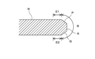
- FIG. 1A is an enlarged cross-sectional view showing a peripheral portion of a wafer, which is an example of a substrate.
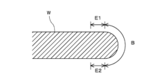
- FIG. 1B is an enlarged sectional view showing a peripheral portion of a wafer, which is an example of a substrate.
- FIG. 2A is a schematic diagram showing an example of a stacked wafer in which two wafers are bonded.
- FIG. 2B is a schematic diagram showing a stacked wafer after the second wafer shown in FIG. 2A is ground (thinned).
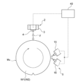
- FIG. 1 is a diagram showing an embodiment of a substrate manufacturing apparatus.
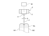
- FIG. 4A is a diagram showing how the filler is applied to the stacked wafers.
- FIG. 4B is a diagram showing the size of the filler applied to the stacked wafers.
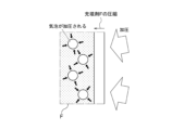
- FIG. 6A is a diagram showing how pressurized fluid is injected into gaps between stacked wafers.
- FIG. 6B is a diagram showing how pressurized fluid is injected into gaps between stacked wafers. It is a figure showing other embodiments of a coating device.
- FIG. 3 is a diagram showing a curing device for curing filler applied to gaps between stacked wafers.
- FIG. 3 is a diagram showing a combination of a fluid ejecting device as a bubble removing device and a curing device.
- FIGS. 1A and 1B are enlarged cross-sectional views showing the peripheral edge of a wafer, which is an example of a substrate. More specifically, FIG. 1A is a sectional view of a so-called straight wafer, and FIG. 1B is a sectional view of a so-called round wafer.
- the bevel portion is the outermost peripheral surface of the wafer W, which is composed of an upper inclined portion (upper bevel portion) P, a lower inclined portion (lower bevel portion) Q, and a side portion (apex) R. (denoted by symbol B).
- the bevel portion is a portion (indicated by the symbol B) that constitutes the outermost peripheral surface of the wafer W and has a curved cross section.
- the top edge portion E1 is a region located inside the beveled portion B in the radial direction and is a flat portion located radially outside the region D in which the device is formed.
- the top edge portion E1 may include a region where a device is formed.
- the bottom edge portion E2 is a flat portion located on the opposite side to the top edge portion E1 and located radially inward than the bevel portion B.
- FIG. 2A is a schematic diagram showing an example of a stacked wafer made by bonding two wafers together
- FIG. 2B is a schematic diagram showing the stacked wafer after the second wafer shown in FIG. 2A is ground (thinned).
- the stacked wafer Ws shown in FIG. 2A is manufactured by bonding the round-shaped first wafer W1 and second wafer W2 shown in FIG. 1B.
- a knife edge portion NE is formed at the peripheral edge of the second wafer W2.
- This knife edge portion NE is easily chipped due to physical contact, and as a result, there is a risk that defects such as cracks and chips may occur in the stacked wafer Ws. Therefore, by applying a filler between the first wafer W1 and the second wafer W2 of the stacked wafer Ws and hardening the filler, the knife edge portion NE is effectively protected.
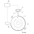
- FIG. 3 is a diagram showing an embodiment of a substrate manufacturing apparatus.
- the substrate manufacturing apparatus is an apparatus that manufactures (that is, processes) a stacked wafer Ws formed by bonding a first wafer W1 and a second wafer W2. Therefore, the substrate manufacturing apparatus may also be called a substrate processing apparatus.
- the substrate manufacturing apparatus fills the gap between the substrate holding device 1 that holds the stacked wafers Ws and the bevel portion B of the first wafer W1 and the bevel portion B of the second wafer W2 (that is, the gap between the stacked wafers Ws). It includes a coating device 2 for coating the filler F, and a bubble removing device 5 for removing bubbles from the filler F applied to the gaps between the stacked wafers Ws.
- the substrate holding device 1 is a device that rotates the stacked wafers Ws while holding the stacked wafers Ws vertically by vacuum suction, but the substrate holding device 1 rotates the stacked wafers Ws horizontally. It may be configured to be rotated while being held in the same direction.
- the substrate holding device 1 may be a combination of a plurality of holding rollers. Even with such a combination, the substrate holding device 1 can rotate the stacked wafers Ws while holding the stacked wafers Ws in the vertical direction.
- the coating device 2 is arranged above the stacked wafers Ws held in the vertical direction. More specifically, the stacked wafers Ws are held with their planes perpendicular to the horizontal plane. In other words, the stacked wafers Ws are held vertically.
- the coating device 2 includes a supply nozzle 4 that supplies the filler F toward the gaps between the stacked wafers Ws, and a support arm 3 that supports the supply nozzle 4.
- the bubble removal device 5 includes a vibration device 10 that vibrates the stacked wafers Ws through the substrate holding device 1.
- the vibration device 10 is, for example, an ultrasonic vibrator.
- the vibration device 10 can vibrate the filler F applied to the gap between the stacked wafers Ws through the stacked wafers Ws by vibrating the stacked wafers Ws.
- the vibration device 10 vibrates the air bubbles mixed in the filler F to bond adjacent air bubbles to each other.
- the joined bubbles become large bubbles and are discharged (degassed) to the outside of the filler F.
- the bubble removal device 5 (more specifically, the vibration device 10) can remove bubbles from the filler F applied to the gaps between the stacked wafers Ws.
- FIG. 4A is a diagram showing how the filler is applied to the stacked wafers
- FIG. 4B is a diagram showing the size of the filler applied to the stacked wafers.
- the substrate manufacturing apparatus includes a control device 40 that controls the operations of the substrate holding device 1, the coating device 2, and the bubble removing device 5.
- the control device 40 operates the substrate holding device 1 and the coating device 2 to rotate the stacked wafers Ws, and supplies the filler F from above the stacked wafers Ws through the supply nozzle 4.
- the gaps between the stacked wafers Ws are filled with the filler F over the entire circumference of the stacked wafers Ws (see FIG. 4A).
- the size D (i.e., line width) of the filler F applied from the supply nozzle 4 is 0.2 to 0.3 mm, and the size of the gap between the stacked wafers Ws. It corresponds to
- the control device 40 operates the bubble removal device 5 (more specifically, the vibration device 10) to vibrate the stacked wafers Ws when applying the filler F to the gaps between the stacked wafers Ws. Air bubbles are removed from the filler F applied to the gaps between the stacked wafers Ws. The control device 40 continues the vibration by the vibration device 10 until the air bubbles are removed from the filler F. After applying the filler F to the gaps between the stacked wafers Ws, a grinding process is performed to grind (thin) the first wafer W1 or the second wafer W2.
- the bubble removal device 5 can remove bubbles from the filler F applied to the gaps between the stacked wafers Ws. Therefore, the substrate manufacturing apparatus can prevent defects such as cracks and chips from occurring in the knife edge portion NE due to air bubbles mixed in the filler F.
- FIG. 5 is a diagram showing another embodiment of the bubble removing device.
- the bubble removing device 5 includes fluid ejecting devices 15 and 16 that eject pressurized fluid onto the filler F applied to the gaps between the stacked wafers Ws.
- a pressurized fluid is a fluid that has been imbued with kinetic energy.
- pressurized fluid means a gas (eg, nitrogen gas) pressurized to the pressure necessary to remove air bubbles from the filler F.
- the fluid ejecting devices 15 and 16 are arranged adjacent to each other in the vertical direction, and are configured to locally inject pressurized fluid onto the filler F above the gap between the stacked wafers Ws. It is configured.
- the bubble removal device 5 may comprise at least one of the fluid ejection devices 15,16.
- FIGS. 6A and 6B are diagrams showing how pressurized fluid is injected into gaps between stacked wafers.
- the control device 40 is electrically connected to each of the fluid ejection devices 15 and 16, and can independently control each of the fluid ejection devices 15 and 16.
- the filler F is compressed by locally injecting pressurized fluid onto the filler F above the gap between the stacked wafers Ws.
- the air bubbles mixed in the filler F are compressed together with the filler F, and eventually become small to the extent that they do not adversely affect the knife edge portion NE.
- the size of the bubbles reduced by the injection of pressurized fluid does not return to its original size. In this way, the bubble removal device 5 can remove bubbles from the filler F applied to the gaps between the stacked wafers Ws.
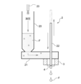
- FIG. 7 is a diagram showing another embodiment of the coating device.
- the applicator 2 includes a syringe body 20 filled with filler F, an introduction section 21 that introduces the filler F in the syringe body 20 into the supply nozzle 4 through the support arm 3, and an introduction section.
- the syringe may include a rod 22 that pushes out the filler F in the syringe body 21 to the supply nozzle 4, and an injection nozzle 23 that injects pressurized fluid (for example, nitrogen gas) to the filler in the syringe body 20.
- pressurized fluid for example, nitrogen gas
- the filler F in the syringe body 20 may already contain air bubbles. Therefore, in the embodiment shown in FIG. 7, the injection nozzle 23 injects pressurized fluid to the filler F supplied to the supply nozzle 4 (that is, the filler F in the syringe main body 20) to form the stacked wafer Ws. It is configured to remove air bubbles from the filler F before it is applied to the gap.
- the control device 40 is configured to be able to control the operation of the injection nozzle 23. More specifically, controller 40 is electrically connected to a fluid source (not shown) that supplies pressurized fluid through injection nozzle 23 . By injecting the pressurized fluid from the injection nozzle 23, the air bubbles mixed into the filler F in the syringe body 20 are compressed together with the filler F, and eventually become small to the extent that they do not adversely affect the knife edge portion NE. (See Figures 6A and 6B).
- the control device 40 is configured to be able to control the operation of the rod 22. More specifically, the control device 40 is electrically connected to a vertical movement device (not shown) that moves the rod 22 up and down.
- a vertical movement device (not shown) that moves the rod 22 up and down.
- An example of the rod 22 is a piston rod.
- the filler F in the introduction section 21 is supplied through the supply nozzle 4 toward the gap between the stacked wafers Ws. Ru.
- air bubbles can be removed from the filler F before it is applied to the gaps between the stacked wafers Ws, so that the knife edge portion NE may not be cracked due to air bubbles mixed in the filler F. Defects such as chipping can be prevented from occurring.
- the embodiment shown in FIG. 3, the embodiment shown in FIG. 5, and the embodiment shown in FIG. 7 can be combined as appropriate. Such a combination allows air bubbles mixed into the filler F to be removed more effectively.
- the substrate manufacturing apparatus may include only the configuration according to the embodiment shown in FIG. 7 instead of including the bubble removing device 5 (see FIGS. 3 and 5).
- FIG. 8 is a diagram showing a curing device for curing the filler applied to the gaps between stacked wafers.
- the substrate manufacturing apparatus may include a curing device 30 that hardens the filler F applied to the gaps between the stacked wafers Ws.
- the control device 40 is electrically connected to the curing device 30 and can control the operation of the curing device 30.
- the curing device 30 when employing the filler F that is cured by irradiation with ultraviolet rays, the curing device 30 may be an ultraviolet irradiation device that irradiates the filler F with ultraviolet rays to cure the filler F. .
- the curing device 30 when employing a filler F that hardens with moisture, the curing device 30 may be a mist supply device that supplies mist to the filler F to harden the filler F.
- the curing device 30 may be a heater that heats the filler F by supplying gas at a high temperature (that is, the temperature necessary to cure the filler F) to the filler F. In other words, the temperature required to cure the filler F is the curing temperature.
- the substrate manufacturing apparatus may include a coating device 2, a bubble removal device 5 (more specifically, a vibration device 10), and a curing device 30.
- a coating device 2 a bubble removal device 5 (more specifically, a vibration device 10), and a curing device 30.
- the substrate manufacturing apparatus may further include an injection nozzle 23 (see FIG. 7) that injects pressurized fluid onto the filler F supplied to the supply nozzle 4.
- FIG. 9 is a diagram showing a combination of a fluid injection device as a bubble removal device and a curing device.
- the substrate manufacturing apparatus may include fluid ejecting devices 15 and 16 and a curing device 30.
- the substrate manufacturing apparatus may further include an injection nozzle 23 (see FIG. 7) that injects pressurized fluid onto the filler F supplied to the supply nozzle 4.
- the curing device 30 is arranged downstream of the fluid ejecting devices 15 and 16 in the rotation direction of the stacked wafers Ws.
- the fluid ejecting devices 15 and 16 are arranged between the supply nozzle 4 and the curing device 30 in the rotation direction of the stacked wafers Ws.
- At least one of the fluid ejection devices 15, 16 may have the same functionality as the curing device 30.
- the fluid ejecting device 16 disposed downstream of the fluid ejecting device 15 in the rotation direction of the stacked wafer Ws may be configured to eject heated fluid. With such a configuration, air bubbles in the filler F supplied from the supply nozzle 4 are removed by the fluid injection device 15, and then the filler F is rapidly hardened.
- the bubble removing device 5 may include not only the fluid ejecting devices 15 and 16 but also the vibrating device 10.
- the present invention can be used in a substrate manufacturing method and a substrate manufacturing apparatus.
Landscapes
- Mechanical Treatment Of Semiconductor (AREA)
- Application Of Or Painting With Fluid Materials (AREA)
- Internal Circuitry In Semiconductor Integrated Circuit Devices (AREA)
- Die Bonding (AREA)
Abstract
Description
一態様では、前記気泡を除去する工程は、前記隙間に塗布された充填剤に加圧流体を噴射する工程を含む。
一態様では、前記基板製造方法は、前記隙間に塗布される前の充填剤から気泡を除去する工程を含む。
一態様では、前記基板製造方法は、前記積層基板を研削する工程を含む。
一態様では、前記気泡除去装置は、前記隙間に塗布された充填剤に加圧流体を噴射する流体噴射装置を備えている。
一態様では、前記塗布装置は、前記隙間に向けて充填剤を供給する供給ノズルに供給される充填剤に加圧流体を噴射する噴射ノズルを備えている。
一態様では、前記硬化装置は、前記基板の回転方向において、前記隙間に塗布された充填剤に加圧流体を噴射する流体噴射装置の下流側に配置されている。
2 塗布装置
3 支持アーム
4 供給ノズル
5 気泡除去装置
10 振動装置
15,16 流体噴射装置
20 シリンジ本体
21 導入部
22 ロッド
23 噴射ノズル
30 硬化装置
40 制御装置
Claims (12)
- 第1基板および第2基板を貼り合わせて形成された積層基板を製造する基板製造方法において、
前記第1基板のベベル部と前記第2基板のベベル部との間の隙間に充填剤を塗布する工程と、
前記隙間に塗布された充填剤から気泡を除去する工程と、を含む、基板製造方法。 - 前記気泡を除去する工程は、前記積層基板を保持する基板保持装置を通じて前記積層基板を振動させる工程を含む、請求項1に記載の基板製造方法。
- 前記気泡を除去する工程は、前記隙間に塗布された充填剤に加圧流体を噴射する工程を含む、請求項1に記載の基板製造方法。
- 前記基板製造方法は、前記隙間に塗布される前の充填剤から気泡を除去する工程を含む、請求項1に記載の基板製造方法。
- 前記基板製造方法は、前記気泡を除去する工程の後に、前記隙間に塗布された充填剤を硬化させる工程を含む、請求項1に記載の基板製造方法。
- 前記基板製造方法は、前記積層基板を研削する工程を含む、請求項1に記載の基板製造方法。
- 第1基板および第2基板を貼り合わせて形成された積層基板を製造する基板製造装置において、
前記第1基板のベベル部と前記第2基板のベベル部との間の隙間に充填剤を塗布する塗布装置と、
前記隙間に塗布された充填剤から気泡を除去する気泡除去装置と、を備える、基板製造装置。 - 前記気泡除去装置は、前記積層基板を保持する基板保持装置を通じて前記積層基板を振動させる振動装置を備えている、請求項7に記載の基板製造装置。
- 前記気泡除去装置は、前記隙間に塗布された充填剤に加圧流体を噴射する流体噴射装置を備えている、請求項7に記載の基板製造装置。
- 前記塗布装置は、前記隙間に向けて充填剤を供給する供給ノズルに供給される充填剤に加圧流体を噴射する噴射ノズルを備えている、請求項7に記載の基板製造装置。
- 前記基板製造装置は、前記隙間に塗布された充填剤を硬化させる硬化装置を備えている、請求項7に記載の基板製造装置。
- 前記硬化装置は、前記基板の回転方向において、前記隙間に塗布された充填剤に加圧流体を噴射する流体噴射装置の下流側に配置されている、請求項11に記載の基板製造装置。
Priority Applications (2)
| Application Number | Priority Date | Filing Date | Title |
|---|---|---|---|
| KR1020257003865A KR20250036173A (ko) | 2022-07-13 | 2023-06-15 | 기판 제조 방법 및 기판 제조 장치 |
| CN202380052720.XA CN119522484A (zh) | 2022-07-13 | 2023-06-15 | 基板制造方法及基板制造装置 |
Applications Claiming Priority (2)
| Application Number | Priority Date | Filing Date | Title |
|---|---|---|---|
| JP2022112208A JP2024010745A (ja) | 2022-07-13 | 2022-07-13 | 基板製造方法および基板製造装置 |
| JP2022-112208 | 2022-07-13 |
Publications (1)
| Publication Number | Publication Date |
|---|---|
| WO2024014221A1 true WO2024014221A1 (ja) | 2024-01-18 |
Family
ID=89536418
Family Applications (1)
| Application Number | Title | Priority Date | Filing Date |
|---|---|---|---|
| PCT/JP2023/022221 Ceased WO2024014221A1 (ja) | 2022-07-13 | 2023-06-15 | 基板製造方法および基板製造装置 |
Country Status (5)
| Country | Link |
|---|---|
| JP (1) | JP2024010745A (ja) |
| KR (1) | KR20250036173A (ja) |
| CN (1) | CN119522484A (ja) |
| TW (1) | TW202403838A (ja) |
| WO (1) | WO2024014221A1 (ja) |
Citations (3)
| Publication number | Priority date | Publication date | Assignee | Title |
|---|---|---|---|---|
| US20080268614A1 (en) * | 2007-04-25 | 2008-10-30 | Ku-Feng Yang | Wafer Bonding |
| JP2022017700A (ja) * | 2020-07-14 | 2022-01-26 | 株式会社荏原製作所 | 基板処理方法、および基板処理装置 |
| JP2022038834A (ja) * | 2020-08-27 | 2022-03-10 | 株式会社荏原製作所 | 基板処理方法、および基板処理装置 |
Family Cites Families (2)
| Publication number | Priority date | Publication date | Assignee | Title |
|---|---|---|---|---|
| JP4788256B2 (ja) * | 2005-09-15 | 2011-10-05 | Tdk株式会社 | 多層基板の製造方法 |
| JP2007129077A (ja) * | 2005-11-04 | 2007-05-24 | Casio Comput Co Ltd | 半導体装置の製造方法及び脱泡装置 |
-
2022
- 2022-07-13 JP JP2022112208A patent/JP2024010745A/ja active Pending
-
2023
- 2023-06-15 WO PCT/JP2023/022221 patent/WO2024014221A1/ja not_active Ceased
- 2023-06-15 CN CN202380052720.XA patent/CN119522484A/zh active Pending
- 2023-06-15 KR KR1020257003865A patent/KR20250036173A/ko active Pending
- 2023-07-10 TW TW112125604A patent/TW202403838A/zh unknown
Patent Citations (3)
| Publication number | Priority date | Publication date | Assignee | Title |
|---|---|---|---|---|
| US20080268614A1 (en) * | 2007-04-25 | 2008-10-30 | Ku-Feng Yang | Wafer Bonding |
| JP2022017700A (ja) * | 2020-07-14 | 2022-01-26 | 株式会社荏原製作所 | 基板処理方法、および基板処理装置 |
| JP2022038834A (ja) * | 2020-08-27 | 2022-03-10 | 株式会社荏原製作所 | 基板処理方法、および基板処理装置 |
Also Published As
| Publication number | Publication date |
|---|---|
| JP2024010745A (ja) | 2024-01-25 |
| KR20250036173A (ko) | 2025-03-13 |
| TW202403838A (zh) | 2024-01-16 |
| CN119522484A (zh) | 2025-02-25 |
Similar Documents
| Publication | Publication Date | Title |
|---|---|---|
| JP6475519B2 (ja) | 保護部材の形成方法 | |
| JP6429388B2 (ja) | 積層デバイスの製造方法 | |
| TW202416363A (zh) | 晶圓之加工方法 | |
| CN110911309B (zh) | 压电振动板、超声波水喷射装置和超声波变幅器 | |
| KR20200091337A (ko) | 캐리어판의 제거 방법 | |
| CN109219865B (zh) | 基板处理方法及基板处理装置 | |
| KR20240049338A (ko) | 기판 처리 방법 및 기판 처리 장치 | |
| JP6991673B2 (ja) | 剥離方法 | |
| JP2015095547A (ja) | ウェーハの分割方法 | |
| WO2024014221A1 (ja) | 基板製造方法および基板製造装置 | |
| KR20080055505A (ko) | 웨이퍼 후면 액상접착제 도포를 이용한 반도체 패키지 제조용 인라인 시스템 | |
| US12087589B2 (en) | Method of manufacturing wafer and method of manufacturing stacked device chip | |
| TWI845749B (zh) | 載板之除去方法 | |
| JP5744486B2 (ja) | 保護膜剥離装置 | |
| JP5552466B2 (ja) | 接合方法、プログラム、コンピュータ記憶媒体及び接合システム | |
| JP2024010749A (ja) | 基板保持装置、基板製造装置、および基板製造方法 | |
| JP5437049B2 (ja) | 板状部材の保持装置および保持方法 | |
| JP3946107B2 (ja) | 半導体装置の製造装置及び半導体装置の製造方法 | |
| TW202407761A (zh) | 填充劑塗布裝置 | |
| JP6116155B2 (ja) | ウエーハの加工方法 | |
| TW202316573A (zh) | 基板處理方法 | |
| WO2024166656A1 (ja) | 基板処理装置 | |
| JP6260416B2 (ja) | 板状物の加工方法 | |
| JP2024053801A (ja) | 液状樹脂供給装置 | |
| JP2026065839A (ja) | 処理方法、チップの製造方法および薄化済ウェーハの製造方法 |
Legal Events
| Date | Code | Title | Description |
|---|---|---|---|
| 121 | Ep: the epo has been informed by wipo that ep was designated in this application |
Ref document number: 23839396 Country of ref document: EP Kind code of ref document: A1 |
|
| WWE | Wipo information: entry into national phase |
Ref document number: 202380052720.X Country of ref document: CN |
|
| ENP | Entry into the national phase |
Ref document number: 20257003865 Country of ref document: KR Kind code of ref document: A |
|
| WWE | Wipo information: entry into national phase |
Ref document number: 1020257003865 Country of ref document: KR |
|
| NENP | Non-entry into the national phase |
Ref country code: DE |
|
| WWP | Wipo information: published in national office |
Ref document number: 202380052720.X Country of ref document: CN |
|
| WWP | Wipo information: published in national office |
Ref document number: 1020257003865 Country of ref document: KR |
|
| 122 | Ep: pct application non-entry in european phase |
Ref document number: 23839396 Country of ref document: EP Kind code of ref document: A1 |