WO2024014173A1 - 圧延銅箔、銅張積層板、銅張積層板の製造方法、フレキシブルプリント配線板の製造方法及び電子部品の製造方法 - Google Patents
圧延銅箔、銅張積層板、銅張積層板の製造方法、フレキシブルプリント配線板の製造方法及び電子部品の製造方法 Download PDFInfo
- Publication number
- WO2024014173A1 WO2024014173A1 PCT/JP2023/020562 JP2023020562W WO2024014173A1 WO 2024014173 A1 WO2024014173 A1 WO 2024014173A1 JP 2023020562 W JP2023020562 W JP 2023020562W WO 2024014173 A1 WO2024014173 A1 WO 2024014173A1
- Authority
- WO
- WIPO (PCT)
- Prior art keywords
- copper foil
- rolled copper
- manufacturing
- grain boundary
- clad laminate
- Prior art date
- Legal status (The legal status is an assumption and is not a legal conclusion. Google has not performed a legal analysis and makes no representation as to the accuracy of the status listed.)
- Ceased
Links
Images

Classifications
-
- C—CHEMISTRY; METALLURGY
- C22—METALLURGY; FERROUS OR NON-FERROUS ALLOYS; TREATMENT OF ALLOYS OR NON-FERROUS METALS
- C22C—ALLOYS
- C22C9/00—Alloys based on copper
-
- C—CHEMISTRY; METALLURGY
- C22—METALLURGY; FERROUS OR NON-FERROUS ALLOYS; TREATMENT OF ALLOYS OR NON-FERROUS METALS
- C22F—CHANGING THE PHYSICAL STRUCTURE OF NON-FERROUS METALS AND NON-FERROUS ALLOYS
- C22F1/00—Changing the physical structure of non-ferrous metals or alloys by heat treatment or by hot or cold working
- C22F1/08—Changing the physical structure of non-ferrous metals or alloys by heat treatment or by hot or cold working of copper or alloys based thereon
-
- H—ELECTRICITY
- H05—ELECTRIC TECHNIQUES NOT OTHERWISE PROVIDED FOR
- H05K—PRINTED CIRCUITS; CASINGS OR CONSTRUCTIONAL DETAILS OF ELECTRIC APPARATUS; MANUFACTURE OF ASSEMBLAGES OF ELECTRICAL COMPONENTS
- H05K1/00—Printed circuits
- H05K1/02—Details
-
- H—ELECTRICITY
- H05—ELECTRIC TECHNIQUES NOT OTHERWISE PROVIDED FOR
- H05K—PRINTED CIRCUITS; CASINGS OR CONSTRUCTIONAL DETAILS OF ELECTRIC APPARATUS; MANUFACTURE OF ASSEMBLAGES OF ELECTRICAL COMPONENTS
- H05K1/00—Printed circuits
- H05K1/02—Details
- H05K1/03—Use of materials for the substrate
-
- H—ELECTRICITY
- H05—ELECTRIC TECHNIQUES NOT OTHERWISE PROVIDED FOR
- H05K—PRINTED CIRCUITS; CASINGS OR CONSTRUCTIONAL DETAILS OF ELECTRIC APPARATUS; MANUFACTURE OF ASSEMBLAGES OF ELECTRICAL COMPONENTS
- H05K1/00—Printed circuits
- H05K1/02—Details
- H05K1/09—Use of materials for the conductive, e.g. metallic pattern
-
- C—CHEMISTRY; METALLURGY
- C22—METALLURGY; FERROUS OR NON-FERROUS ALLOYS; TREATMENT OF ALLOYS OR NON-FERROUS METALS
- C22F—CHANGING THE PHYSICAL STRUCTURE OF NON-FERROUS METALS AND NON-FERROUS ALLOYS
- C22F1/00—Changing the physical structure of non-ferrous metals or alloys by heat treatment or by hot or cold working
Definitions
- the present invention relates to rolled copper foil, copper-clad laminates, methods for manufacturing copper-clad laminates, methods for manufacturing flexible printed wiring boards, and methods for manufacturing electronic components.
- a flexible printed wiring board is a board in which a metal, which is a conductive layer, and a flexible insulating substrate, typically a resin film, are bonded together. Copper foil is generally used for the conductive layer, and rolled copper foil, which has excellent flexibility, is used especially in applications where flexibility is required.
- a typical FPC manufacturing process is as follows. First, the copper foil is bonded to the resin film. Bonding can be accomplished by applying a varnish containing a precursor of polyimide resin onto the copper foil and applying heat treatment to imidize it (casting method), or by laminating a resin film with adhesive strength and the copper foil. There is a method (laminate method). The resin film-attached copper foil bonded through these steps is called a copper clad laminate (CCL). Thereafter, wiring is formed by etching, and the FPC is completed.
- rolled copper foil for FPC is required to have flexibility.
- Patent Document 1 in order to provide a rolled copper foil for FPC that is easily annealed at the curing temperature of the resin adhesive and has extremely good bending resistance (flexural fatigue life) after annealing, the final cold working degree is It has been proposed that the ratio should be 90% or more.
- the inventors of the present invention found that when rolled copper foil is heat-treated under predetermined conditions, the arithmetic mean value of the grain boundary density is 38.40 mm -1 or less, resulting in rolled copper foil with high flexibility. They discovered that copper foil can be obtained and created the invention illustrated by the following. [1] Contains 99.9% by mass or more of Cu, the remainder consisting of unavoidable impurities, Grain boundary density measured at three points, one arbitrary point and two points equally spaced 5 mm apart from it in the direction perpendicular to the rolling direction, when heat treated at a dryer temperature of 260°C and a heating holding time of 30 minutes.
- a rolled copper foil having an arithmetic mean value of 38.40 mm -1 or less [2] The rolled copper foil according to [1], further containing 100 to 360 mass ppm of Ag. [3] The rolled copper foil according to any one of [1] to [2], having a thickness of 4 to 35 ⁇ m. [4] The rolled copper foil according to any one of [1] to [3], wherein the arithmetic mean value of the grain boundary density is 0.1 mm -1 or more. [5] Copper having rolled copper foil having an arithmetic mean value of grain boundary density of 38.40 mm -1 or less measured at one arbitrary point and two points equally spaced apart by 5 mm in the direction perpendicular to rolling. Tension laminate.
- [6] The copper-clad laminate according to [5], which has a rolled copper foil in which the arithmetic mean value of the grain boundary density is 0.1 mm -1 or more.
- a method for manufacturing a copper-clad laminate comprising the step of bonding the rolled copper foil according to any one of [1] to [4] and a base material, and in the step, heat treatment is performed.
- a method for manufacturing a flexible printed wiring board comprising a step of forming wiring using a copper-clad laminate manufactured by the method for manufacturing a copper-clad laminate according to [7].
- a method for manufacturing an electronic component comprising the step of manufacturing an electronic component including a flexible printed wiring board manufactured by the method for manufacturing a flexible printed wiring board according to [8].
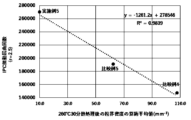
- FIG. 3 is a schematic diagram showing the measurement method of the IPC sliding bending test in Example 5 and Comparative Examples 4 and 5. This is a graph plotting the arithmetic mean value of grain boundary density after heat treatment at 260° C. for 30 minutes on the horizontal axis and the number of times of IPC sliding bending on the vertical axis based on Example 5 and Comparative Examples 4 and 5.
- the present invention is not limited to the embodiments described below, and can be embodied by modifying the constituent elements within the scope of the invention. Moreover, various inventions can be formed by appropriately combining a plurality of components disclosed in each embodiment.
- rolling direction means a direction parallel to the direction in which the object to be rolled passes between a pair of work rolls.
- direction perpendicular to rolling means a direction perpendicular to the rolling direction on the rolling surface.
- the unit of grain boundary density "mm -1 " means “mm/mm 2 ".
- the rolled copper foil according to the present invention contains 99.9% by mass or more of Cu, with the remainder consisting of unavoidable impurities.
- the rolled copper foil may be composed of pure Cu.
- the rolled copper foil contains Ag as an alloying element in a total of 100 to 100%, from the viewpoint of controlling the recrystallization temperature to an appropriate level while more reliably obtaining higher flexibility than before when converted into FPC. It may further contain 360 ppm by mass.
- the recrystallization temperature of the rolled copper foil becomes high, so that recrystallization may be insufficient even if heat treatment is performed by a casting method or a lamination method. If unrecrystallized grains remain in the rolled copper foil, the flexibility of the FPC will be significantly reduced. Moreover, if the Ag content is 100 mass ppm or more, the amount of rolling strain introduced will increase, so the grain boundary density after CCL heat treatment will tend to decrease, and the flexibility will tend to increase.
- the upper limit of the oxygen content in the rolled copper foil is, for example, 500 mass ppm or less. Further, the lower limit of the oxygen content in the rolled copper foil is, for example, 0 mass ppm or more. From the viewpoint of reducing the amount of cuprous oxide (CuO) in the material, which is considered to have an adverse effect on the flexibility of FPC, the oxygen content is preferably 50 mass ppm or less.
- the composition of the rolled copper foil according to the present invention can be measured by fluorescent X-ray analysis as dry analysis.
- the fluorescent X-ray analysis is performed using Simultix 14 manufactured by Rigaku Corporation.
- the analysis surface may be one that has been cut or mechanically polished so that the surface maximum height roughness Rz (JIS B0601:2013) is 6.3 ⁇ m or less.
- ICP-OES ICP optical emission spectrometer
- the rolled copper foil according to the present invention has an arithmetic average grain boundary density when heat-treated rolled copper foil is measured by the method described below at an internal temperature of a dryer of 260° C. and a heating holding time of 30 minutes. The value is 38.40 mm -1 or less. Specifically, a part of the rolled copper foil was taken as a sample, and the sample was placed in a dryer (DRH453WA manufactured by Advantech Toyo Co., Ltd.) maintained at 260°C, and after heat treatment for 30 minutes in the air. Then, take it out of the dryer and let it cool in the air.
- a dryer DVR453WA manufactured by Advantech Toyo Co., Ltd.
- the sample was placed between two sheets of phosphor bronze (JIS H 3110 (C5210)).
- a laminate is made by sandwiching the laminate between plates (thickness: 0.2 mm), and the laminate is wrapped and sealed with rolled copper foil (thickness: 33 ⁇ m) made of sufficiently annealed tough pitch copper, and then placed in a dryer.
- a rolled copper foil whose grain boundary density is within a prescribed range under prescribed heat treatment conditions has relatively few high-angle grain boundaries where the orientation difference between adjacent crystal grains is 15° or more, so it is difficult to form grain boundaries during bending. Strain is less likely to accumulate.
- the grain boundary density can be measured on the surface of the rolled copper foil and a cross section in the thickness direction (a cross section perpendicular to the surface of the rolled copper foil).
- the thickness of the rolled copper foil of the present invention is smaller than the crystal grain size, crystal growth in the thickness direction is suppressed. grains elongated in the direction) are measured. Therefore, the value of the grain boundary density between the surface of the rolled copper foil and the cross section in the thickness direction is significantly different.
- the grain boundary density on the surface of the rolled copper foil is several tens of tens of times lower than the grain boundary density on the cross section in the thickness direction. It is easy to show a value about twice as large.
- the measured value of the grain boundary density of a cross section in the thickness direction tends to have a large difference depending on the observation position within the cross section. The present inventors believe that controlling the conditions is important from the viewpoint of ensuring flexibility.
- the arithmetic mean value of the grain boundary density is 38.40 mm -1 or less on the upper limit side.
- the lower limit of the arithmetic mean value of the grain boundary density is typically 0.1 mm -1 or more. If the arithmetic mean value of the grain boundary density is too small, the accumulation of strain due to fatigue will concentrate on a few grain boundaries, making it more likely that fractures will occur starting at those grain boundaries, which may have a negative impact on flexibility. . Therefore, in order to control the arithmetic mean value of the grain boundary density after heat treatment within a predetermined range, the inventor of the present invention found that control of the average grain size after final annealing and the working degree of final cold rolling are important. discovered. The conditions of the average grain size after the final annealing and the working degree of the final cold rolling will be described later and will therefore be omitted.
- EBSD Electron Back Scatter Diffraction
- Kikuchi line diffraction Kikuchi pattern
- the rolled copper foil as a whole is bent. They tend to be highly sexual. This is because, although some variation may occur in the manufacturing conditions to some extent during the manufacturing process, the grain boundary density measured after heat treatment of the rolled copper foil obtained in the manufacturing process under predetermined conditions is generally controlled within the desired range.
- the rolled copper foil Although it is possible that there may be some areas where the arithmetic mean value of grain boundary density exceeds 38.40 mm -1 , it is assumed that such areas are not so large, and most of them have the desired metal structure. , the problems of the present invention can be solved. Furthermore, due to manufacturing and handling of rolled copper foil (for example, cutting out samples for measurement), abnormal areas such as excessive oil pits, adhesion of foreign matter, and rolling streaks may occur in some areas.
- measurement locations should be set to avoid locations that correspond to abnormal areas.
- Abnormal areas can be identified by observing the sample before electrolytic polishing using a SEM (observation magnification: 100x). If the measurement point and the abnormal area overlap, measure at a total of 3 points, avoiding the abnormal area.
- ⁇ Blend of electrolyte solution > ⁇ 250ml distilled water ⁇ Phosphoric acid 125ml ⁇ Urea 2.5g ⁇ Ethanol grade 1 125ml ⁇ 1-propanol 25ml ⁇ Electrolytic polishing conditions> Applied voltage: 10V Electrolysis time: 10 seconds ⁇ EBSD measurement conditions, etc.> ⁇ SEM conditions Equipment: Scanning electron microscope manufactured by JEOL Ltd.
- Type of electron gun Electrolytic emission type electron gun (Schottky type) Electron gun emitter: ZrO tungsten cathode Objective lens type: Out-lens type Focus correction: Yes (dynamic focus: 50) Beam conditions Acceleration voltage: 15kV Working distance: 15mm Irradiation current amount: 15nA SEM probe diameter: 0.5-2nm Observation magnification: 90x, EBSD device conditions Detector: Slow scan CCD camera, manufactured by TSL Solutions Co., Ltd., data processing conditions Data collection software: OIM Data Collection, manufactured by TSL Solutions Co., Ltd.
- OIM Analysis V8 manufactured by TSL Solutions Co., Ltd. is used for data analysis.
- ⁇ Data analysis conditions of OIM Analysis V8> ⁇ New Map window Map Style Grayscale: Select ⁇ None>. Color Coded: Select Crystal Orientation.
- Type Select Rotation Angle.
- Rotation Angle tab Define Range: Minimum input value: 15 Maximum input value: 180 Use only boundaries between identified checkbox: Do not enter. After converting the Length value in the measurement results of Boundaries: Rotation Angle conducted under the above setting conditions to mm, the value divided by the observation range (1 mm x 1 mm) is defined as the grain boundary density.
- the rolled copper foil according to the present invention has an average crystal grain size of more than 15 ⁇ m and less than 35 ⁇ m before final cold rolling and after recrystallization annealing 3 (final annealing) in the manufacturing examples described below. suitable.
- the smaller the crystal grain size the easier it is to accumulate dislocation strain that becomes the driving force for primary recrystallization during final rolling. Therefore, by setting the average crystal grain size before the final cold rolling and after the final annealing to more than 15 ⁇ m and less than 35 ⁇ m, the grains grow large during the heat treatment of the rolled copper foil, and the arithmetic mean value of the grain boundary density can be maintained at a predetermined value.
- the flexibility is improved.
- the average grain size after final annealing is 35 ⁇ m or more, dislocation strain will not easily accumulate during final cold rolling, and shear bands will likely develop in the rolled structure. Since shear bands inhibit the growth of crystal grains during heat treatment of rolled copper foil, grain boundary density is difficult to reduce.
- the average crystal grain size is measured by EBSD on the sample surface after final annealing. After electrolytic polishing is performed under the above-mentioned conditions to remove a thickness of approximately 1 ⁇ m from the surface of the sample, an arbitrarily set observation range of 1000 ⁇ m ⁇ 1000 ⁇ m is scanned with a step size of 3 ⁇ m. Thereafter, analysis is performed using the Area Fraction method, and the average crystal grain size is measured when boundaries where the crystal orientation difference exceeds 5° are regarded as grain boundaries. OIM Analysis V8 manufactured by TSL Solutions Co., Ltd. is used for the above analysis. The EBSD measurement conditions not shown below are as described above.
- the thickness of the rolled copper foil is, for example, 4 to 35 ⁇ m.
- the upper limit of the thickness of the rolled copper foil is, for example, 35 ⁇ m or less, and 18 ⁇ m or less, and the lower limit is, for example, 4 ⁇ m or more, 6 ⁇ m or more, and, for example, 9 ⁇ m or more.
- an X-ray generator is placed on the surface side of the rolled copper foil, an X-ray detector is placed on the other main surface side, and the measured amount of transmitted X-rays is used to determine the thickness of the rolled copper foil.
- the amount of attenuation due to the thickness of the rolled copper foil and converting it to the thickness of the rolled copper foil is measured by determining the amount of attenuation due to the thickness of the rolled copper foil and converting it to the thickness of the rolled copper foil. For example, measure the weight of a 20 cm square rolled copper foil, and calculate the thickness of the rolled copper foil from weight (g)/(density of rolled copper foil (g/cm 3 ) x area of rolled copper foil (cm 2 )). (Note that the density of rolled copper foil is 8.94 g/cm 3 for oxygen-free copper according to JIS H 3100 (C1020), as an example). Further, for example, measurements are performed at two or more arbitrary points using a digital length measuring machine (for example, Nikon's Digimicro MH-15M), and the thickness of the rolled copper foil is calculated from the arithmetic mean value of each thickness.
- a digital length measuring machine for example, Nikon's Digimicro MH-15M
- Example of manufacturing rolled copper foil As an example of a method for manufacturing rolled copper foil, first, a raw material such as copper is melted in a melting furnace to obtain a molten metal having a desired composition. Then, an ingot is manufactured by pouring this molten metal into a mold (casting). To prevent oxidative loss of copper, melting and casting are preferably carried out in vacuum or in an inert gas atmosphere.
- the rolled copper foil is basically the one immediately after the final cold rolling.
- the arithmetic mean value of grain boundary density of rolled copper foil when heat treated at 260°C for 30 minutes is determined by the average grain size after final annealing and It is inferred that it is largely influenced by the degree of work in the final cold rolling.
- Final annealing conditions are appropriately set so that the arithmetic mean value of grain boundary density when heat treated at 260° C. for 30 minutes is controlled within a predetermined range.
- the conditions for final annealing may be appropriately set so that the average grain size after final annealing is more than 15 ⁇ m and less than 35 ⁇ m.
- the conditions may vary depending on the composition of the copper material, those skilled in the art can experimentally determine the annealing conditions without excessive trial and error based on the annealing conditions disclosed in the present examples and comparative examples.
- a rolled copper foil is obtained by performing final cold rolling under conditions of a working degree of more than 98% and less than 99%.
- the thickness of the rolled copper foil at this time is approximately 4 to 35 ⁇ m.
- working degree (%) ⁇ (Thickness before final cold rolling (mm) - Thickness after final cold rolling (mm))/Thickness before final cold rolling (mm) ⁇ Defined as 100.
- An embodiment of the method for manufacturing a copper-clad laminate according to the present invention includes a step of bonding the rolled copper foil described above to a base material.
- the base material include resin films.
- Several techniques can be employed to bond the resin film and rolled copper foil.
- a method can be used in which a rolled copper foil and a polyimide resin film are bonded together using an adhesive made of a thermosetting resin such as epoxy, and then heat-treated.
- a method of forming a polyimide film on at least one surface of the rolled copper foil by applying a varnish containing polyamic acid, which is a precursor of polyimide resin, to at least one surface of the rolled copper foil and curing it by heating.
- the rolled copper foil can be crimped by hot pressing, or by sandwiching a polyimide resin film between two rolled copper foils and heat pressing. There is a method of crimping. These heat treatments are generally carried out at 125 to 360°C for 30 to 400 minutes. Furthermore, there is also a method in which the rolled copper foil and the resin film are laminated using an adhesive without going through a heat treatment process. Examples of the material for the resin film include, but are not limited to, polyester, polyimide, polyethylene terephthalate, polyethylene naphthalate, and the like.
- the rolled copper foil before laminating the rolled copper foil and the resin film, the rolled copper foil can be subjected to a roughening treatment.
- the roughening treatment can be performed under the following conditions. ⁇ Roughening treatment conditions> Liquid composition: Cu10-20g/L, Co1-10g/L, Ni1-15g/L pH: 1-4 Temperature: 30-50°C Current density (Dk): 20-50A/dm 2 Time: 1-5 seconds
- the arithmetic mean value of the grain boundary density measured at three points, one arbitrary point and two points spaced equally apart by 5 mm in the direction perpendicular to the rolling direction is 38.40 mm by the heat treatment. It is possible to produce a copper-clad laminate that has a copper foil (rolled copper foil) and a base material (resin film) that are -1 or less. Note that the method for measuring grain boundary density is the same as the method described above.
- the method for manufacturing a flexible printed wiring board according to the present invention includes a step of forming wiring using a copper-clad laminate manufactured by the method for manufacturing a copper-clad laminate described above. At this time, it is possible to form wiring using the copper-clad laminate as a material according to a known procedure to manufacture a flexible printed wiring board (FPC). For example, an etching resist is applied to the rolled copper foil surface of a copper-clad laminate only on the necessary parts as a conductive pattern, and an etching solution is sprayed onto the rolled copper foil surface to remove unnecessary rolled copper foil and form a conductive pattern. Then, the etching resist is peeled off and removed to expose the conductive pattern. After forming the conductor pattern, it is common to apply a protective coverlay film.
- FPC flexible printed wiring board
- Such FPCs are used in electronic parts such as electronic and electrical equipment such as moving parts in hard disks, hinges and sliding parts of mobile phones, inside mobile phones, printer heads, optical pickup parts, and moving parts of notebook PCs. This applies to FPCs used for etc.
- the method for manufacturing an electronic component may include a step of manufacturing an electronic component including a flexible printed wiring board manufactured by the above method for manufacturing a flexible printed wiring board.
- Examples 1 to 4, Comparative Examples 1 to 3 Manufacture of rolled copper foil]
- the Ag content of the ingot was measured by the above-mentioned ICP emission spectrometry.
- This ingot was processed in the following process order to produce rolled copper foil.
- Step 1 Homogenization annealing: The above ingot was heated and held at 920° C. for 2.5 hours.
- Hot rolling The ingot heated at 920°C was rolled at room temperature to a thickness of 16 mm. Thereafter, it was rapidly cooled to room temperature by water cooling to obtain a band-shaped metal material.
- Step 3) Cold rolling 1: Rolled to a thickness of 10.5 mm.
- Step 4) Recrystallization annealing 1 The above band-shaped metal material was heated and held at 400° C. for 7.5 hours.
- Step 5 Surface cutting: Oxidized scale on the surface was removed by surface cutting.
- Step 6 Cold rolling 2: Rolled to a thickness of 1.5 mm.
- Step 7 Recrystallization annealing 2: The sample was kept in a furnace heated to 750°C for 30 to 120 seconds.
- Step 8) Pickling/polishing: After immersing in a mixed acid of sulfuric acid and hydrogen peroxide, the oxide film on the surface of the material was removed by buffing.
- Step 9) Cold rolling 3: Rolled to a thickness of 0.8 mm.
- Recrystallization annealing 3 (final annealing): The annealing temperature and holding time were adjusted so that a predetermined crystal grain size was obtained, and the band-shaped metal material after cold rolling 3 was heated and held.
- Table 1 lists the annealing conditions for each sample.
- the band-shaped metal material is wrapped and sealed in a rolled copper foil (thickness: 33 ⁇ m) of sufficiently annealed tough pitch copper (JIS H 3100 (C1100)). It was put into the dryer. After maintaining the heat, the sealed body was taken out from the dryer and allowed to cool in the air. After cooling, the band-shaped metal material was taken out from the sealed body. Moreover, the average grain size after final annealing was measured by the method described above. (Step 11) Final cold rolling: Finished to a thickness of 0.012 mm (12 ⁇ m) to obtain a rolled copper foil.
- the strip-shaped metal material is passed between a pair of work rolls without fixing both ends of the strip-shaped metal material in the rolling direction (in a free end state). Rolling was carried out without applying any tension to the material.
- recrystallization annealing 3 was performed at the annealing temperature and holding time listed in Table 1.
- the sealed body which was further wrapped and sealed with a film (thickness: 33 ⁇ m), was placed in a dryer and heat-treated at an internal temperature of 260° C. for 30 minutes. After the heat treatment, it was taken out from the dryer and left to cool in the air. After cooling, the rolled copper foil, which was a measurement sample, was taken out from the sealed body.
- the grain boundary density of the heat-treated rolled copper foil was measured by the method described above using a scanning electron microscope (JSM-IT500HR) manufactured by JEOL Ltd., using the sample surface of the heat-treated rolled copper foil as the measurement target. .
- Tables 1 and 2 show three points measured at 5 mm intervals while avoiding abnormal areas (an arbitrary point N1, a point N2 that is 5 mm away from N1 in the direction perpendicular to the rolling direction, and a point N2 that is 5 mm away from N1 in the direction perpendicular to the rolling direction and from N1 to N2).
- Each value and arithmetic mean value of the grain boundary density at a point N3) located 5 mm away in the direction opposite to the direction toward which the graph is directed are shown.
- N1 to N3 are rounded to the second decimal place, and the arithmetic mean value is calculated from each value up to the first decimal place after rounding, and is also rounded to the second decimal place.
- Example 5 Comparative Examples 4-5
- Example 5 and Comparative Examples 4 and 5 in order to confirm the relationship between the arithmetic mean value of grain boundary density and flexibility, rolled copper having the grain boundary density listed in Table 2 when heat treated at 260°C for 30 minutes was tested.
- Table 2 shows the values and arithmetic average value of grain boundary density at three points measured at 5 mm intervals in the direction perpendicular to rolling, avoiding abnormal areas. The notation of each value and arithmetic mean value is as described above.
- Example 5 a portion of the rolled copper foil before heat treatment at 260° C. for 30 minutes, that is, after final cold rolling, was taken as a sample for measurement.
- Pixio a polyimide resin film manufactured by Kaneka Co., Ltd.
- FRS grade Thickness: 25 ⁇ m
- This IPC bending test device 100 has a structure in which a vibration transmission member 20 is coupled to an oscillation drive body 10, and a test piece 30 has a total of four parts, including a screw 40 portion indicated by an arrow and the tip of the vibration transmission member 20. It is fixed to the device at a point.
- the vibration transmission member 20 is driven up and down, the intermediate portion of the test piece 30 is bent into a hairpin shape with a predetermined radius of curvature r.
- the IPC sliding bending test was conducted under the conditions that the radius of curvature r was 2.5 mm (outer radius), the vibration stroke was 20 mm, and the vibration speed was 1500 times/min.
Landscapes
- Chemical & Material Sciences (AREA)
- Engineering & Computer Science (AREA)
- Microelectronics & Electronic Packaging (AREA)
- Materials Engineering (AREA)
- Mechanical Engineering (AREA)
- Metallurgy (AREA)
- Organic Chemistry (AREA)
- Physics & Mathematics (AREA)
- Thermal Sciences (AREA)
- Crystallography & Structural Chemistry (AREA)
- Metal Rolling (AREA)
- Parts Printed On Printed Circuit Boards (AREA)
Priority Applications (3)
| Application Number | Priority Date | Filing Date | Title |
|---|---|---|---|
| KR1020247038458A KR20250036060A (ko) | 2022-07-14 | 2023-06-01 | 압연 동박, 동장 적층판, 동장 적층판의 제조 방법, 플렉시블 프린트 배선판의 제조 방법 및 전자 부품의 제조 방법 |
| CN202380042762.5A CN119677887A (zh) | 2022-07-14 | 2023-06-01 | 压延铜箔、覆铜层叠板、覆铜层叠板的制造方法、柔性印刷线路板的制造方法以及电子部件的制造方法 |
| JP2024533566A JPWO2024014173A1 (https=) | 2022-07-14 | 2023-06-01 |
Applications Claiming Priority (10)
| Application Number | Priority Date | Filing Date | Title |
|---|---|---|---|
| JP2022-113456 | 2022-07-14 | ||
| JP2022113456 | 2022-07-14 | ||
| JP2022113460 | 2022-07-14 | ||
| JP2022-113460 | 2022-07-14 | ||
| JP2023-060962 | 2023-04-04 | ||
| JP2023060964 | 2023-04-04 | ||
| JP2023060962 | 2023-04-04 | ||
| JP2023060966 | 2023-04-04 | ||
| JP2023-060966 | 2023-04-04 | ||
| JP2023-060964 | 2023-04-04 |
Publications (1)
| Publication Number | Publication Date |
|---|---|
| WO2024014173A1 true WO2024014173A1 (ja) | 2024-01-18 |
Family
ID=89536537
Family Applications (4)
| Application Number | Title | Priority Date | Filing Date |
|---|---|---|---|
| PCT/JP2023/020562 Ceased WO2024014173A1 (ja) | 2022-07-14 | 2023-06-01 | 圧延銅箔、銅張積層板、銅張積層板の製造方法、フレキシブルプリント配線板の製造方法及び電子部品の製造方法 |
| PCT/JP2023/020559 Ceased WO2024014170A1 (ja) | 2022-07-14 | 2023-06-01 | 圧延銅箔、銅張積層板、銅張積層板の製造方法、フレキシブルプリント配線板の製造方法及び電子部品の製造方法 |
| PCT/JP2023/020557 Ceased WO2024014168A1 (ja) | 2022-07-14 | 2023-06-01 | 圧延銅箔、銅張積層板の製造方法、フレキシブルプリント配線板の製造方法及び電子部品の製造方法 |
| PCT/JP2023/020561 Ceased WO2024014172A1 (ja) | 2022-07-14 | 2023-06-01 | 圧延銅箔、銅張積層板、銅張積層板の製造方法、フレキシブルプリント配線板の製造方法及び電子部品の製造方法 |
Family Applications After (3)
| Application Number | Title | Priority Date | Filing Date |
|---|---|---|---|
| PCT/JP2023/020559 Ceased WO2024014170A1 (ja) | 2022-07-14 | 2023-06-01 | 圧延銅箔、銅張積層板、銅張積層板の製造方法、フレキシブルプリント配線板の製造方法及び電子部品の製造方法 |
| PCT/JP2023/020557 Ceased WO2024014168A1 (ja) | 2022-07-14 | 2023-06-01 | 圧延銅箔、銅張積層板の製造方法、フレキシブルプリント配線板の製造方法及び電子部品の製造方法 |
| PCT/JP2023/020561 Ceased WO2024014172A1 (ja) | 2022-07-14 | 2023-06-01 | 圧延銅箔、銅張積層板、銅張積層板の製造方法、フレキシブルプリント配線板の製造方法及び電子部品の製造方法 |
Country Status (4)
| Country | Link |
|---|---|
| JP (4) | JPWO2024014168A1 (https=) |
| KR (4) | KR20250036062A (https=) |
| CN (4) | CN119256110A (https=) |
| WO (4) | WO2024014173A1 (https=) |
Citations (7)
| Publication number | Priority date | Publication date | Assignee | Title |
|---|---|---|---|---|
| JPH02156032A (ja) * | 1988-12-09 | 1990-06-15 | Hitachi Cable Ltd | 電子機器用配線材料及びその製造方法 |
| JP2000256765A (ja) * | 1999-03-08 | 2000-09-19 | Nippon Mining & Metals Co Ltd | 屈曲性に優れるフレキシブルプリント回路基板用圧延銅箔およびその製造方法 |
| JP2011094200A (ja) * | 2009-10-30 | 2011-05-12 | Jx Nippon Mining & Metals Corp | 銅又は銅合金箔、及びそれを用いた両面銅張積層板の製造方法 |
| JP2012243454A (ja) * | 2011-05-17 | 2012-12-10 | Jx Nippon Mining & Metals Corp | 圧延銅箔、並びにこれを用いた負極集電体、負極板及び二次電池 |
| JP2013044005A (ja) * | 2011-08-23 | 2013-03-04 | Jx Nippon Mining & Metals Corp | 両面銅張積層板用圧延銅合金箔、及びそれを用いた両面銅張積層板の製造方法 |
| JP2014214376A (ja) * | 2013-04-30 | 2014-11-17 | 株式会社Shカッパープロダクツ | 圧延銅箔、フレキシブル銅張積層板及びフレキシブルプリント配線板 |
| WO2015182777A1 (ja) * | 2014-05-29 | 2015-12-03 | 古河電気工業株式会社 | 銅合金板材及びその製造方法、前記銅合金板材からなる電気電子部品 |
Family Cites Families (2)
| Publication number | Priority date | Publication date | Assignee | Title |
|---|---|---|---|---|
| JPH04228553A (ja) | 1990-06-22 | 1992-08-18 | Hitachi Cable Ltd | 耐屈曲性圧延銅箔 |
| WO2013021970A1 (ja) * | 2011-08-05 | 2013-02-14 | 古河電気工業株式会社 | 二次電池集電体用圧延銅箔およびその製造方法 |
-
2023
- 2023-06-01 WO PCT/JP2023/020562 patent/WO2024014173A1/ja not_active Ceased
- 2023-06-01 WO PCT/JP2023/020559 patent/WO2024014170A1/ja not_active Ceased
- 2023-06-01 KR KR1020247038463A patent/KR20250036062A/ko active Pending
- 2023-06-01 CN CN202380042735.8A patent/CN119256110A/zh active Pending
- 2023-06-01 CN CN202380042762.5A patent/CN119677887A/zh active Pending
- 2023-06-01 JP JP2024533561A patent/JPWO2024014168A1/ja active Pending
- 2023-06-01 CN CN202380042417.1A patent/CN119256103A/zh active Pending
- 2023-06-01 KR KR1020247037957A patent/KR20250036056A/ko active Pending
- 2023-06-01 KR KR1020247038458A patent/KR20250036060A/ko active Pending
- 2023-06-01 WO PCT/JP2023/020557 patent/WO2024014168A1/ja not_active Ceased
- 2023-06-01 CN CN202380042746.6A patent/CN119301290A/zh active Pending
- 2023-06-01 JP JP2024533563A patent/JPWO2024014170A1/ja active Pending
- 2023-06-01 JP JP2024533566A patent/JPWO2024014173A1/ja active Pending
- 2023-06-01 JP JP2024533565A patent/JPWO2024014172A1/ja active Pending
- 2023-06-01 WO PCT/JP2023/020561 patent/WO2024014172A1/ja not_active Ceased
- 2023-06-01 KR KR1020247038441A patent/KR20250036059A/ko active Pending
Patent Citations (7)
| Publication number | Priority date | Publication date | Assignee | Title |
|---|---|---|---|---|
| JPH02156032A (ja) * | 1988-12-09 | 1990-06-15 | Hitachi Cable Ltd | 電子機器用配線材料及びその製造方法 |
| JP2000256765A (ja) * | 1999-03-08 | 2000-09-19 | Nippon Mining & Metals Co Ltd | 屈曲性に優れるフレキシブルプリント回路基板用圧延銅箔およびその製造方法 |
| JP2011094200A (ja) * | 2009-10-30 | 2011-05-12 | Jx Nippon Mining & Metals Corp | 銅又は銅合金箔、及びそれを用いた両面銅張積層板の製造方法 |
| JP2012243454A (ja) * | 2011-05-17 | 2012-12-10 | Jx Nippon Mining & Metals Corp | 圧延銅箔、並びにこれを用いた負極集電体、負極板及び二次電池 |
| JP2013044005A (ja) * | 2011-08-23 | 2013-03-04 | Jx Nippon Mining & Metals Corp | 両面銅張積層板用圧延銅合金箔、及びそれを用いた両面銅張積層板の製造方法 |
| JP2014214376A (ja) * | 2013-04-30 | 2014-11-17 | 株式会社Shカッパープロダクツ | 圧延銅箔、フレキシブル銅張積層板及びフレキシブルプリント配線板 |
| WO2015182777A1 (ja) * | 2014-05-29 | 2015-12-03 | 古河電気工業株式会社 | 銅合金板材及びその製造方法、前記銅合金板材からなる電気電子部品 |
Also Published As
| Publication number | Publication date |
|---|---|
| WO2024014168A1 (ja) | 2024-01-18 |
| JPWO2024014168A1 (https=) | 2024-01-18 |
| CN119301290A (zh) | 2025-01-10 |
| CN119256103A (zh) | 2025-01-03 |
| WO2024014170A1 (ja) | 2024-01-18 |
| CN119256110A (zh) | 2025-01-03 |
| KR20250036056A (ko) | 2025-03-13 |
| CN119677887A (zh) | 2025-03-21 |
| WO2024014172A1 (ja) | 2024-01-18 |
| JPWO2024014170A1 (https=) | 2024-01-18 |
| JPWO2024014173A1 (https=) | 2024-01-18 |
| JPWO2024014172A1 (https=) | 2024-01-18 |
| KR20250036062A (ko) | 2025-03-13 |
| KR20250036059A (ko) | 2025-03-13 |
| KR20250036060A (ko) | 2025-03-13 |
Similar Documents
| Publication | Publication Date | Title |
|---|---|---|
| JP4716520B2 (ja) | 圧延銅箔 | |
| JP3859384B2 (ja) | 屈曲性に優れるフレキシブルプリント回路基板用圧延銅箔およびその製造方法 | |
| TWI588273B (zh) | Copper alloy foil for flexible printed circuit board, copper-clad laminate using the same, flexible printed circuit board and electronic equipment | |
| US10002684B2 (en) | Copper alloy and method for manufacturing the same | |
| TWI730280B (zh) | 可撓性印刷基板用銅箔、使用其之覆銅積層體、可撓性印刷基板及電子機器 | |
| JP2007107038A (ja) | 回路用銅又は銅合金箔 | |
| WO2012128098A1 (ja) | 圧延銅箔及びその製造方法、並びに銅張積層板 | |
| WO2024014173A1 (ja) | 圧延銅箔、銅張積層板、銅張積層板の製造方法、フレキシブルプリント配線板の製造方法及び電子部品の製造方法 | |
| KR20210007845A (ko) | 플렉시블 프린트 기판용 구리박 | |
| JP2001144391A (ja) | プリント回路基板用圧延銅箔およびその製造方法 | |
| JP2013055162A (ja) | フレキシブルプリント配線板用銅箔、銅張積層板、フレキシブルプリント配線板及び電子機器 | |
| TW202409310A (zh) | 軋製銅箔、覆銅層疊板、覆銅層疊板的製造方法、軟性印刷電路板的製造方法以及電子部件的製造方法 | |
| WO2024014171A1 (ja) | 圧延銅箔、銅張積層板、銅張積層板の製造方法、フレキシブルプリント配線板の製造方法及び電子部品の製造方法 | |
| TW202440955A (zh) | 軋製銅箔、覆銅層疊板、覆銅層疊板的製造方法、柔性印刷線路板的製造方法以及電子部件的製造方法 | |
| TW202442035A (zh) | 軋製銅箔、覆銅層疊板、覆銅層疊板的製造方法、柔性印刷線路板的製造方法以及電子部件的製造方法 | |
| TW202100762A (zh) | 銅合金板、附鍍敷被膜之銅合金板及此等之製造方法 | |
| WO2024014169A1 (ja) | 銅箔並びにそれを用いた銅張積層板及びフレキシブルプリント配線板 | |
| JP2025099491A (ja) | 圧延銅箔、銅張積層板の製造方法、フレキシブルプリント配線板の製造方法及び電子部品の製造方法 | |
| TW202417651A (zh) | 軋製銅箔、覆銅層疊板、覆銅層疊板的製造方法、柔性印刷線路板的製造方法以及電子部件的製造方法 | |
| TW202405195A (zh) | 軋製銅箔、覆銅層疊板的製造方法、柔性印刷線路板的製造方法以及電子部件的製造方法 | |
| TWI539017B (zh) | Rolled copper foil, copper clad laminate, and flexible printed circuit boards and electronic equipment | |
| JP2019214793A (ja) | 圧延銅箔、銅張積層板、フレキシブルプリント配線板、電子機器及び圧延銅箔の製造方法 |
Legal Events
| Date | Code | Title | Description |
|---|---|---|---|
| 121 | Ep: the epo has been informed by wipo that ep was designated in this application |
Ref document number: 23839350 Country of ref document: EP Kind code of ref document: A1 |
|
| ENP | Entry into the national phase |
Ref document number: 2024533566 Country of ref document: JP Kind code of ref document: A |
|
| WWE | Wipo information: entry into national phase |
Ref document number: 202380042762.5 Country of ref document: CN |
|
| NENP | Non-entry into the national phase |
Ref country code: DE |
|
| WWP | Wipo information: published in national office |
Ref document number: 1020247038458 Country of ref document: KR |
|
| WWP | Wipo information: published in national office |
Ref document number: 202380042762.5 Country of ref document: CN |
|
| 122 | Ep: pct application non-entry in european phase |
Ref document number: 23839350 Country of ref document: EP Kind code of ref document: A1 |