WO2024009722A1 - 半導体装置 - Google Patents
半導体装置 Download PDFInfo
- Publication number
- WO2024009722A1 WO2024009722A1 PCT/JP2023/022234 JP2023022234W WO2024009722A1 WO 2024009722 A1 WO2024009722 A1 WO 2024009722A1 JP 2023022234 W JP2023022234 W JP 2023022234W WO 2024009722 A1 WO2024009722 A1 WO 2024009722A1
- Authority
- WO
- WIPO (PCT)
- Prior art keywords
- wires
- wire
- semiconductor device
- thickness direction
- viewed
- Prior art date
- Legal status (The legal status is an assumption and is not a legal conclusion. Google has not performed a legal analysis and makes no representation as to the accuracy of the status listed.)
- Ceased
Links
Images


Classifications
-
- H—ELECTRICITY
- H10—SEMICONDUCTOR DEVICES; ELECTRIC SOLID-STATE DEVICES NOT OTHERWISE PROVIDED FOR
- H10W—GENERIC PACKAGES, INTERCONNECTIONS, CONNECTORS OR OTHER CONSTRUCTIONAL DETAILS OF DEVICES COVERED BY CLASS H10
- H10W72/00—Interconnections or connectors in packages
-
- H—ELECTRICITY
- H10—SEMICONDUCTOR DEVICES; ELECTRIC SOLID-STATE DEVICES NOT OTHERWISE PROVIDED FOR
- H10W—GENERIC PACKAGES, INTERCONNECTIONS, CONNECTORS OR OTHER CONSTRUCTIONAL DETAILS OF DEVICES COVERED BY CLASS H10
- H10W72/00—Interconnections or connectors in packages
- H10W72/071—Connecting or disconnecting
Definitions
- the present disclosure relates to a semiconductor device.
- Patent Document 1 discloses an example of a conventional semiconductor device.
- the semiconductor device disclosed in this document includes a semiconductor element, a plurality of leads, a plurality of wires, and a sealing resin.
- a semiconductor element is mounted on one of the plurality of leads.
- Each of the plurality of wires is bonded to a semiconductor element and another lead different from the lead on which the semiconductor element is mounted.
- the other lead has a plurality of terminal portions.
- the other leads are adjacent to the lead on which the semiconductor element is mounted in a certain direction (downward in the paper in FIG. 3 of Patent Document 1) on the side where the plurality of terminal parts are arranged. It is located.
- the sealing resin covers part of each of the plurality of leads, the plurality of wires, and the semiconductor element.
- An object of the present disclosure is to provide a semiconductor device that is improved over conventional ones.
- an object of the present disclosure is to provide a semiconductor device suitable for efficiently arranging a plurality of wires in a semiconductor element.
- a semiconductor device provided by a first aspect of the present disclosure includes a first lead having a first surface facing one side in the thickness direction, a semiconductor element supported on the first surface, and a first end of each lead. a plurality of wires having a section and a second end.
- the semiconductor element has an element main surface facing one side in the thickness direction, and a main surface electrode formed on the element main surface.
- the first end of each of the plurality of wires is joined to the main surface electrode.
- the plurality of wires include one or more first wires and one or more second wires. At least one of the one or more second wires straddles at least one of the one or more first wires when viewed in the thickness direction.
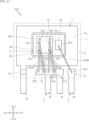
- FIG. 1 is a plan view showing a semiconductor device according to a first embodiment of the present disclosure.
- FIG. 2 is a plan view showing a semiconductor device according to the first embodiment of the present disclosure.
- FIG. 3 is a sectional view taken along line III-III in FIG. 2.
- FIG. 4 is a cross-sectional view taken along line IV-IV in FIG. 2.
- FIG. 5 is a sectional view taken along line VV in FIG. 2.
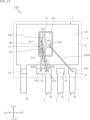
- FIG. 6 is a right side view showing the semiconductor device according to the first embodiment of the present disclosure.
- FIG. 7 is a plan view showing a semiconductor device according to a first modification of the first embodiment.
- FIG. 8 is a right side view showing a semiconductor device according to a first modification of the first embodiment.
- FIG. 1 is a plan view showing a semiconductor device according to a first embodiment of the present disclosure.
- FIG. 2 is a plan view showing a semiconductor device according to the first embodiment of the present disclosure.
- FIG. 3 is a sectional view taken
- FIG. 9 is a plan view showing a semiconductor device according to a second modification of the first embodiment.
- FIG. 10 is a right side view showing a semiconductor device according to a second modification of the first embodiment.
- FIG. 11 is a plan view showing a semiconductor device according to a third modification of the first embodiment.
- FIG. 12 is a right side view showing a semiconductor device according to a third modification of the first embodiment.
- FIG. 13 is a plan view showing a semiconductor device according to a fourth modification of the first embodiment.
- FIG. 14 is a right side view showing a semiconductor device according to a fourth modification of the first embodiment.
- FIG. 15 is a plan view showing a semiconductor device according to a fifth modification of the first embodiment.
- FIG. 10 is a right side view showing a semiconductor device according to a second modification of the first embodiment.
- FIG. 11 is a plan view showing a semiconductor device according to a third modification of the first embodiment.
- FIG. 12 is a right side view showing a semiconductor device according to
- FIG. 16 is a right side view showing a semiconductor device according to a fifth modification of the first embodiment.
- FIG. 17 is a plan view showing a semiconductor device according to a second embodiment of the present disclosure.
- FIG. 18 is a right side view showing a semiconductor device according to a second embodiment of the present disclosure.
- a thing A is formed on a thing B and "a thing A is formed on a thing B” mean “a thing A is formed on a thing B” unless otherwise specified.
- "something A is placed on something B” and “something A is placed on something B” mean "something A is placed on something B” unless otherwise specified.
- a certain surface A faces (one side or the other side of) the direction B is not limited to the case where the angle of the surface A with respect to the direction B is 90 degrees; Including cases where it is tilted to the opposite direction.
- First embodiment 1 to 6 show a semiconductor device according to a first embodiment of the present disclosure.
- the semiconductor device A10 of this embodiment includes a first lead 1, a second lead 2, a third lead 3, a fourth lead 4, a semiconductor element 5, a plurality of wires 6, and a sealing resin 7.
- FIG. 1 and 2 are plan views showing the semiconductor device A10.
- FIG. 3 is a sectional view taken along line III-III in FIG. 2.
- FIG. 4 is a cross-sectional view taken along line IV-IV in FIG. 2.
- FIG. 5 is a sectional view taken along line VV in FIG. 2.
- FIG. 6 is a right side view showing the semiconductor device A10. Note that in FIG. 2, the sealing resin 7 is shown for convenience of understanding. 6 shows the view through the sealing resin 7 and omits the third lead 3, the fourth lead 4, and some of the plurality of wires 6 (the third wire 63 and the fourth wire 64, which will be described later). There is.
- the thickness direction of the semiconductor element 5 is referred to as the "thickness direction z.”
- One direction perpendicular to the thickness direction z is an example of a “first direction” and will be referred to as a “first direction x.”
- a direction perpendicular to both the thickness direction z and the first direction x is an example of a "second direction” and will be referred to as a “second direction y.”
- the first lead 1, second lead 2, third lead 3, and fourth lead 4 are formed, for example, by punching or bending a metal plate (lead frame).
- the thicknesses of the first lead 1, second lead 2, third lead 3, and fourth lead 4 are not particularly limited, and are, for example, about 0.1 mm to 2.0 mm.
- the constituent material of the first lead 1, second lead 2, third lead 3, and fourth lead 4 is, for example, copper (Cu), nickel (Ni), or an alloy thereof. Although detailed illustrations and explanations are omitted, most of the first lead 1, second lead 2, third lead 3, and fourth lead 4 are covered with, for example, a plating layer.
- the constituent material of the plating layer is not particularly limited, and is made of, for example, an alloy containing tin (Sn) as a main component.
- the first lead 1, second lead 2, third lead 3, and fourth lead 4 are arranged apart from each other when viewed in the thickness direction z (in plan view).
- the first lead 1 has the largest size in the thickness direction z-view.
- the first lead 1 has a die pad 11, a first terminal portion 12, and a bent portion 13.
- the die pad 11 has a rectangular shape, for example, when viewed in the thickness direction z.
- Die pad 11 has a first surface 11a and a second surface 11b.
- the first surface 11a faces the z1 side in the thickness direction z
- the second surface 11b faces the opposite side to the first surface 11a (the z2 side in the thickness direction z).
- the first surface 11a supports the semiconductor element 5.
- the entire die pad 11 is covered with the sealing resin 7.
- Die pad 11 is an example of a "base”.
- the first terminal portion 12 is located on the x1 side of the first direction x with respect to the die pad 11.
- the first terminal portion 12 extends on the x1 side in the first direction x.
- the first terminal portion 12 is located at the end of the die pad 11 on the y1 side in the second direction y.
- the first terminal portion 12 is exposed from the sealing resin 7.
- the bent portion 13 connects the die pad 11 and the first terminal portion 12, and has a bent shape when viewed in the second direction y.
- the second lead 2 has a pad portion 21 and a second terminal portion 22.
- the pad portion 21 is located on the x1 side in the first direction x with respect to the die pad 11 when viewed in the thickness direction z.
- the pad portion 21 extends along the second direction y.
- the second terminal portion 22 is connected to the end of the pad portion 21 on the y2 side in the second direction y, and extends on the x1 side in the first direction x.
- the second terminal portion 22 is exposed from the sealing resin 7.
- the second lead 2 is located on the y2 side in the second direction y with respect to the first terminal portion 12 when viewed in the thickness direction z.
- the third lead 3 has a pad portion 31 and a third terminal portion 32.
- the pad portion 31 is located on the x1 side in the first direction x with respect to the die pad 11 when viewed in the thickness direction z.
- the third terminal portion 32 is connected to the pad portion 31 and extends toward the x1 side in the first direction x.
- the third terminal portion 32 is exposed from the sealing resin 7.
- the third lead 3 is located on the y2 side in the second direction y with respect to the second lead 2 when viewed in the thickness direction z.
- the third lead 3 is located at the end of the die pad 11 on the y2 side in the second direction y.
- the fourth lead 4 has a pad portion 41 and a fourth terminal portion 42.
- the pad portion 41 is located on the x1 side in the first direction x with respect to the die pad 11 when viewed in the thickness direction z.
- the fourth terminal section 42 is connected to the pad section 41 and extends toward the x1 side in the first direction x.
- the fourth terminal portion 42 is exposed from the sealing resin 7.
- the fourth lead 4 is located on the y2 side in the second direction y with respect to the second lead 2 when viewed in the thickness direction z.
- the fourth lead 4 is located between the second lead 2 and the third lead 3 in the second direction y.
- the semiconductor element 5 is an element that performs the electrical functions of the semiconductor device A10.
- the type of semiconductor element 5 is not particularly limited, and in this embodiment, the semiconductor element 5 is configured as a transistor.
- the semiconductor element 5 is a switching element, and is, for example, an n-channel MOSFET, but may also be a p-channel MOSFET.
- the semiconductor element 5 includes an element body 50, a first main surface electrode 51, a second main surface electrode 52, and a back electrode 53.
- the element body 50 has a rectangular shape when viewed in the thickness direction z. More specifically, the element main body 50 (semiconductor element 5) has a long rectangular shape with the second direction y as the longitudinal direction and the first direction x as the lateral direction.
- the element body 50 has an element main surface 50a and an element back surface 50b.
- the element main surface 50a and the element back surface 50b face opposite sides in the thickness direction z.
- the element main surface 50a faces the same side as the first surface 11a of the die pad 11 in the thickness direction z. Therefore, the element back surface 50b faces the first surface 11a.
- the first main surface electrode 51 and the second main surface electrode 52 are arranged on the element main surface 50a.
- the back electrode 53 is arranged on the element back surface 50b.
- the constituent materials of the first main surface electrode 51, the second main surface electrode 52, and the back surface electrode 53 are not particularly limited, and include, for example, a Ti/Ni/Au film, a Ti/Ni/Au/Ag film, a Ti/Ni/Ag film, etc. Consisting of
- the first main surface electrode 51 is arranged in a region from the center of the element main surface 50a in the second direction y to the y1 side in the second direction y.
- the first principal surface electrode 51 has a rectangular shape when viewed in the thickness direction z, and the lengths of each side along the first direction x and the second direction y are approximately the same.
- the first main surface electrode 51 is a source electrode, and is an electrode used as an input/output terminal.
- the second main surface electrode 52 is arranged in a region of the element main surface 50a on the y2 side in the second direction y.
- the second main surface electrode 52 is a gate electrode, and is an electrode to which a gate voltage is applied to the semiconductor element 5 as a switching element.
- the area of the first main surface electrode 51 is significantly larger than the area of the second main surface electrode 52.
- the area of the first main surface electrode 51 also becomes smaller, so the ratio of the area of the first main surface electrode 51 to the area of the second main surface electrode 52 becomes relatively small ( (See FIG. 15 below).
- the first main surface electrode 51 and the second main surface electrode 52 are each an example of a "main surface electrode.”
- the back electrode 53 covers the entire surface (or substantially the entire surface) of the element back surface 50b.
- the back electrode 53 is a drain electrode, and, together with the first main surface electrode 51, is an electrode used as an input/output terminal.
- the back electrode 53 is electrically bonded to the first surface 11a (die pad 11) via a conductive bonding material 59.
- the conductive bonding material 59 electrically connects the die pad 11 and the back electrode 53.
- the conductive bonding material 59 is, for example, solder.
- the first terminal portion 12 of the first lead 1 is electrically connected to the back electrode 53 of the semiconductor element 5 via the die pad 11 and the conductive bonding material 59.
- the first terminal portion 12 is the drain terminal of the semiconductor device A10.
- the semiconductor element 5 is relatively small in size with respect to the die pad 11.
- the semiconductor element 5 is arranged on the first surface 11a of the die pad 11 at approximately the center in each of the first direction x and the second direction y.
- the plurality of wires 6 are connected to one of the first main surface electrode 51 and the second main surface electrode 52 in the semiconductor element 5, the second lead 2, the third lead 3, and the fourth lead. 4.
- the constituent material of each of the plurality of wires 6 is not particularly limited, and includes, for example, gold (Au), aluminum, or copper. In this embodiment, the constituent material of each wire 6 includes, for example, aluminum.
- the plurality of wires 6 include a plurality of first wires 61 , second wires 62 , third wires 63 , and fourth wires 64 .
- Each of the plurality of (two in this embodiment) first wires 61 is joined to the first main surface electrode 51 and the second lead 2.
- Each of the plurality of first wires 61 has a first end 611 and a second end 612.
- the first end portion 611 is joined to the first main surface electrode 51.
- the second end portion 612 is joined to the pad portion 21 of the second lead 2.
- each of the plurality of first wires 61 is bonded to the first main surface electrode 51 and the pad portion 21 (second lead 2) by wedge bonding.
- the plurality of first wires 61 are lined up at intervals in the second direction y, and are arranged parallel to each other when viewed in the thickness direction z.
- the plurality of first wires 61 being parallel to each other refers not only to the case where the plurality of first wires 61 are parallel to each other, but also to the case where the plurality of first wires 61 are slightly deviated from parallel due to manufacturing errors, etc. shall be included.
- "parallel”, which will be described later also includes cases in which there is a slight deviation from parallelism due to manufacturing errors or the like. Note that, unlike the illustrated example, the plurality of first wires 61 may be arranged non-parallel when viewed in the thickness direction z.
- each first wire 61 the second end 612 is located on the y2 side in the second direction y with respect to the first end 611. Furthermore, the first ends 611 of the two first wires 61 shown in FIG. 2 are located at different positions in the first direction x when viewed in the thickness direction z. The first end 611 of the first wire 61 located on the y1 side in the second direction y is more x1 in the first direction x than the first end 611 of the first wire 61 located on the y2 side in the second direction y. located on the side. The second ends 612 of each of the two first wires 61 are located at approximately the same position in the first direction x when viewed in the thickness direction z.
- the second wire 62 is connected to the first main surface electrode 51 and the second lead 2.
- the second wire 62 has a first end 621 and a second end 622.
- the first end portion 621 is joined to the first main surface electrode 51.
- the second end portion 622 is joined to the pad portion 21 of the second lead 2.
- the second wire 62 is bonded to the first main surface electrode 51 and the pad portion 21 (second lead 2) by wedge bonding.
- the second wire 62 extends generally along the first direction x when viewed in the thickness direction z.
- the second wire 62 straddles a plurality of (two) first wires 61 when viewed in the thickness direction z.
- the first end 621 of the second wire 62 is located closer to the x2 side in the first direction x than the first end 611 of each of the plurality of first wires 61 when viewed in the thickness direction z.
- the second wire 62 overlaps the first end portion 611 of each of the plurality of (two) first wires 61 when viewed in the thickness direction z. , straddles the two first ends 611. Note that, unlike the example shown in FIG.
- the second wire 62 is connected to each of the plurality of first wires 61. It is arranged so as to straddle the first end 611 .
- the second end 622 of the second wire 62 is located on the y1 side in the second direction y with respect to the second end 612 of each of the two first wires 61.
- the second end portion 622 is located at approximately the same position as the second end portion 612 of each first wire 61 in the first direction x when viewed in the thickness direction z.
- the second ends 612 of the two first wires 61 and the second ends 622 of the second wires 62 overlap each other when viewed in the second direction y.
- the second terminal portion 22 of the second lead 2 is electrically connected to the first main surface electrode 51 of the semiconductor element 5 via the pad portion 21, the plurality of first wires 61, and the second wire 62. There is.
- the second terminal section 22 is a source terminal of the semiconductor device A10.
- the third wire 63 is connected to the second main surface electrode 52 and the third lead 3.
- the third wire 63 has a first end 631 and a second end 632.
- the first end portion 631 is joined to the second main surface electrode 52.
- the second end portion 632 is joined to the pad portion 31 of the third lead 3.
- the third terminal portion 32 of the third lead 3 is electrically connected to the second main surface electrode 52 of the semiconductor element 5 via the pad portion 31 and the third wire 63.
- the third terminal portion 32 is the gate terminal of the semiconductor device A10.
- the fourth wire 64 is connected to the first main surface electrode 51 and the fourth lead 4.
- the fourth wire 64 has a first end 641 and a second end 642.
- the first end portion 641 is joined to the first main surface electrode 51.
- the second end portion 642 is joined to the pad portion 41 of the fourth lead 4.
- the fourth terminal portion 42 of the fourth lead 4 is electrically connected to the second main surface electrode 52 of the semiconductor element 5 via the pad portion 41 and the fourth wire 64.
- the fourth terminal section 42 functions as a source sense terminal.
- the source sense terminal is a terminal for detecting the potential of the first main surface electrode 51 (source electrode).
- the sealing resin 7 covers parts of each of the first lead 1 , the second lead 2 , the third lead 3 , and the fourth lead 4 , the semiconductor element 5 , and the plurality of wires 6 .
- the sealing resin 7 is made of, for example, black epoxy resin.
- the sealing resin 7 has a resin main surface 71, a resin back surface 72, and resin side surfaces 731 to 734.
- the resin main surface 71 and the resin back surface 72 face opposite sides in the thickness direction z and are spaced apart from each other.
- the main resin surface 71 faces the z1 side in the thickness direction z, and faces the same side as the element main surface 50a and the first surface 11a.
- the resin back surface 72 faces the z2 side in the thickness direction z, and faces the same side as the element back surface 50b and the second surface 11b.
- Each of the resin side surfaces 731 to 734 is connected to the resin main surface 71 and the resin back surface 72, and is sandwiched between the resin main surface 71 and the resin back surface 72 in the thickness direction z.
- the resin side surface 731 and the resin side surface 732 face opposite to each other in the first direction x.
- the resin side surface 731 faces the x1 side in the first direction x
- the resin side surface 732 faces the x2 side in the first direction x.
- the resin side surface 733 and the resin side surface 734 face opposite to each other in the second direction y.
- the resin side surface 733 faces the y1 side in the second direction y
- the resin side surface 734 faces the y2 side in the second direction y.
- each of the first terminal portion 12 , the second terminal portion 22 , the third terminal portion 32 , and the fourth terminal portion 42 protrudes from the resin side surface 731 .
- the resin side surfaces 731 to 734 are each slightly inclined with respect to the thickness direction z.
- the shape of the sealing resin 7 shown in FIGS. 1 and 3 to 5 is an example.
- the shape of the sealing resin 7 is not limited to the illustrated shape.
- the second surface 11b of the die pad 11 is covered with the sealing resin 7, but unlike this, the second surface 11b is covered with the sealing resin 7. It may be configured such that it is not covered by the resin and is exposed from the resin back surface 72 of the sealing resin 7.
- the plurality of wires 6 include a first wire 61 and a second wire 62.
- the first end 611 of the first wire 61 and the first end 621 of the second wire 62 are joined to the first main surface electrode 51 of the semiconductor element 5 .
- the second wire 62 straddles the first wire 61 when viewed in the thickness direction z. According to such a configuration, it is possible to efficiently arrange the plurality of wires 6 (the first wire 61 and the second wire 62) in the relatively small-sized semiconductor element 5.
- the plurality of wires 6 include a plurality of (two) first wires 61, and the second wire 62 straddles the plurality of (two) first wires 61 when viewed in the thickness direction z.
- the first ends 611 of the plurality of (two) first wires 61 are arranged at different positions in the first direction x.
- the second wire 62 straddles the first ends 611 of each of the plurality of (two) first wires 61 when viewed in the thickness direction z. According to such a configuration, the first wires 61 and the second wires 62 can be efficiently arranged in a narrow space while avoiding mutual interference between the plurality of first wires 61 and second wires 62. .
- the plurality of first wires 61 are arranged parallel to each other when viewed in the thickness direction z.
- the second ends 612 of the plurality of (two) first wires 61 and the second ends 622 of the second wires 62 overlap each other when viewed in the second direction y.
- Such a configuration is more preferable for efficiently arranging the first wires 61 and the second wires 62 while avoiding mutual interference between the first wires 61 and the second wires 62.
- FIG. 7 and 8 show a semiconductor device A11 according to a first modification of the first embodiment.
- FIG. 7 is a plan view showing the semiconductor device A11.
- FIG. 8 is a right side view showing the semiconductor device A11.
- the sealing resin 7 is shown.
- the sealing resin 7 is penetrated, and the third lead 3, the fourth lead 4, and some of the plurality of wires 6 (the third wire 63 and the fourth wire 64) are omitted.
- elements that are the same as or similar to those of the semiconductor device A10 of the above embodiment are given the same reference numerals as those of the above embodiment, and the description thereof will be omitted as appropriate.
- the configurations of the respective parts in each modification can be combined with each other as appropriate within a range that does not cause technical contradiction.
- the arrangement of the semiconductor element 5, the plurality of first wires 61, and the arrangement of the second wires 62 are different from the semiconductor device A10 of the above embodiment.
- the semiconductor element 5 is arranged on the first surface 11a of the die pad 11 closer to the y2 side in the second direction y.
- the plurality of first wires 61 are lined up at intervals in the second direction y, and are arranged parallel to each other when viewed in the thickness direction z.
- the second end portion 612 of each of the plurality of (two) first wires 61 is located on the y1 side in the second direction y with respect to the first end portion 611.
- the first ends 611 of the two first wires 61 shown in FIG. 7 are at different positions in the first direction x when viewed in the thickness direction z.
- the first end portion 611 of the first wire 61 located on the y1 side in the second direction y is larger than the first end portion 611 of the first wire 61 on the y2 side in the second direction y. located on the side.
- the second ends 612 of each of the two first wires 61 are located at approximately the same position in the first direction x when viewed in the thickness direction z. Note that, unlike the example shown in FIG. 7, the plurality of first wires 61 may be arranged non-parallel when viewed in the thickness direction z.
- the second wire 62 extends generally along the first direction x when viewed in the thickness direction z.
- the second wire 62 straddles a plurality of (two) first wires 61 when viewed in the thickness direction z.
- the first end 621 of the second wire 62 is located closer to the x2 side in the first direction x than the first end 611 of each of the plurality of first wires 61 when viewed in the thickness direction z.
- the second wire 62 overlaps the first end portion 611 of each of the plurality of (two) first wires 61 when viewed in the thickness direction z, and straddles two first ends 611. Note that, unlike the example shown in FIG.
- the second wire 62 is connected to the first wire of each of the plurality of first wires 61. It is arranged so as to straddle one end 611 .
- the second end 622 of the second wire 62 is located on the y2 side in the second direction y with respect to the second end 612 of each of the two first wires 61.
- the second end portion 622 is located at approximately the same position as the second end portion 612 of each first wire 61 in the first direction x when viewed in the thickness direction z.
- the second ends 612 of the two first wires 61 and the second ends 622 of the second wires 62 overlap each other when viewed in the second direction y.
- the first end 611 of the first wire 61 and the first end 621 of the second wire 62 are joined to the first main surface electrode 51 of the semiconductor element 5.
- the second wire 62 straddles the first wire 61 when viewed in the thickness direction z. According to such a configuration, it is possible to efficiently arrange the plurality of wires 6 (the first wire 61 and the second wire 62) in the relatively small-sized semiconductor element 5.
- the plurality of wires 6 include a plurality of (two) first wires 61, and the second wire 62 straddles the plurality of (two) first wires 61 when viewed in the thickness direction z.
- the first ends 611 of the plurality of (two) first wires 61 are arranged at different positions in the first direction x.
- the second wire 62 straddles the first ends 611 of each of the plurality of (two) first wires 61 when viewed in the thickness direction z. According to such a configuration, the first wires 61 and the second wires 62 can be efficiently arranged in a narrow space while avoiding mutual interference between the plurality of first wires 61 and second wires 62. .
- the plurality of first wires 61 are arranged parallel to each other when viewed in the thickness direction z.
- the second ends 612 of the plurality of (two) first wires 61 and the second ends 622 of the second wires 62 overlap each other when viewed in the second direction y.
- Such a configuration is more preferable for efficiently arranging the first wires 61 and the second wires 62 while avoiding mutual interference between the first wires 61 and the second wires 62.
- FIG. 9 and 10 show a semiconductor device A12 according to a second modification of the first embodiment.
- FIG. 9 is a plan view showing the semiconductor device A12.
- FIG. 10 is a right side view showing the semiconductor device A12.
- the sealing resin 7 is shown.
- the sealing resin 7 is penetrated, and the third lead 3, the fourth lead 4, and some of the plurality of wires 6 (the third wire 63 and the fourth wire 64) are omitted.
- the plurality of wires 6 include the plurality of second wires 62.
- a plurality of (two in this modified example) second wires 62 are lined up at intervals in the second direction y, and are arranged parallel to each other when viewed in the thickness direction z. There is. Unlike the illustrated example, the plurality of second wires 62 may be arranged non-parallel when viewed in the thickness direction z.
- the plurality of first wires 61 are lined up at intervals in the second direction y, and are arranged parallel to each other when viewed in the thickness direction z.
- the second end 612 is located on the y2 side in the second direction y with respect to the first end 611.
- the first end 611 of the first wire 61 located on the y1 side in the second direction y is more x1 in the first direction x than the first end 611 of the first wire 61 located on the y2 side in the second direction y. located on the side.
- the second ends 612 of each of the two first wires 61 are located at approximately the same position in the first direction x when viewed in the thickness direction z. Note that, unlike the example shown in FIG. 9, the plurality of first wires 61 may be arranged non-parallel when viewed in the thickness direction z.
- Each of the plurality of (two) second wires 62 extends generally along the first direction x when viewed in the thickness direction z.
- Each of the two second wires 62 straddles a plurality of (two) first wires 61 when viewed in the thickness direction z.
- the first end 621 of each second wire 62 is located closer to the x2 side in the first direction x than the first end 611 of each of the plurality of first wires 61 when viewed in the thickness direction z.
- the second wire 62 located on the y1 side in the second direction y is the same as the first wire 62 located on the y1 side in the second direction y when viewed in the thickness direction z. 61 , and straddles the first end 611 .
- the second ends 622 of each of the two second wires 62 are located on the y1 side in the second direction y with respect to the second ends 612 of each of the two first wires 61.
- Each second end 622 is located at approximately the same position as the second end 612 of each first wire 61 in the first direction x when viewed in the thickness direction z.
- the second ends 612 of the two first wires 61 and the second ends 622 of the two second wires 62 are mutually connected to each other when viewed in the second direction y. overlapping.
- the first end 611 of the first wire 61 and the first end 621 of the second wire 62 are joined to the first main surface electrode 51 of the semiconductor element 5.
- the second wire 62 straddles the first wire 61 when viewed in the thickness direction z. According to such a configuration, it is possible to efficiently arrange the plurality of wires 6 (the first wire 61 and the second wire 62) in the relatively small-sized semiconductor element 5.
- the plurality of wires 6 include a plurality (two) of first wires 61 and a plurality (two) of second wires 62.
- Each of the plurality of (two) second wires 62 straddles the plurality of (two) first wires 61 when viewed in the thickness direction z.
- the first ends 611 of the plurality of (two) first wires 61 are arranged at different positions in the first direction x.
- One second wire 62 (in this modification, the second wire 62 located on the y1 side in the second direction y) is connected to one first wire 61 (on the y1 side in the second direction y) when viewed in the thickness direction z. straddles the first end 611 of the first wire 61) located on the side. According to such a configuration, it is possible to efficiently arrange the first wires 61 and the second wires 62 in a narrow space while avoiding mutual interference between the plurality of first wires 61 and the plurality of second wires 62. Can be
- the plurality of first wires 61 are arranged parallel to each other when viewed in the thickness direction z.
- the plurality of second wires 62 are arranged parallel to each other when viewed in the thickness direction z.
- the second ends 612 of each of the plurality of (two) first wires 61 and the second ends 622 of each of the plurality of (two) second wires 62 overlap each other when viewed in the second direction y. .
- Such a configuration is more preferable for efficiently arranging the first wires 61 and the second wires 62 while avoiding mutual interference between the first wires 61 and the second wires 62.
- FIG. 11 and 12 show a semiconductor device A13 according to a third modification of the first embodiment.
- FIG. 11 is a plan view showing the semiconductor device A13.
- FIG. 12 is a right side view showing the semiconductor device A13.
- the sealing resin 7 is shown.
- the sealing resin 7 is penetrated, and the third lead 3 and a part of the plurality of wires 6 (the third wire 63) are omitted.
- the plurality of wires 6 include a plurality (four) of first wires 61 and a plurality (two) of second wires 62.
- the semiconductor device A13 of this modification does not include the fourth lead 4 and the fourth wire 64.
- the second lead 2 the dimension of the pad portion 21 in the second direction y is increased, and two second terminal portions 22 connected to the pad portion 21 are provided. These two second terminal portions 22 are arranged at intervals in the second direction y.
- the cross-sectional area of the path through which the main current flows is increased, making it suitable for a large current in the semiconductor device A13.
- the cross-sectional area of the main current path increases, it can be expected that the heat generated in the semiconductor element 5 can be efficiently released to the outside, and the reliability of the semiconductor device A13 can be improved.
- the first end 611 of the first wire 61 and the first end 621 of the second wire 62 are joined to the first main surface electrode 51 of the semiconductor element 5.
- the second wire 62 straddles the first wire 61 when viewed in the thickness direction z. According to such a configuration, it is possible to efficiently arrange the plurality of wires 6 (the first wire 61 and the second wire 62) in the relatively small-sized semiconductor element 5.
- the plurality of wires 6 include a plurality (four) of first wires 61 and a plurality (two) of second wires 62.
- One of the two second wires 62 (the second wire 62 located on the y1 side in the second direction y) is connected to the two first wires 61 (the second wire 62 located on the y1 side in the second direction y) when viewed in the thickness direction z. It straddles two first wires 61) located on the sides.
- the first ends 611 of the two first wires 61 are arranged at different positions in the first direction x.
- One of the second wires 62 (the second wire 62 located on the y1 side in the second direction y) straddles the first ends 611 of each of the two first wires 61 when viewed in the thickness direction z.
- the other of the two second wires 62 (the second wire 62 located on the y2 side in the second direction y) is connected to the other two first wires 61 (the second wire 62 located on the y2 side in the second direction y) when viewed in the thickness direction z. It straddles the two first wires 61) located on the y2 side.
- the first ends 611 of the other two first wires 61 are arranged at different positions in the first direction x.
- the other second wire 62 (the second wire 62 located on the y2 side in the second direction y) straddles the first ends 611 of the other two first wires 61 when viewed in the thickness direction z. According to such a configuration, it is possible to efficiently arrange the first wires 61 and the second wires 62 in a narrow space while avoiding mutual interference between the plurality of first wires 61 and the plurality of second wires 62. Can be done.
- the plurality of first wires 61 are arranged parallel to each other when viewed in the thickness direction z.
- the second ends 612 of each of the plurality of (four) first wires 61 and the second ends 622 of each of the plurality of (two) second wires 62 overlap each other when viewed in the second direction y.
- Such a configuration is more preferable for efficiently arranging the first wires 61 and the second wires 62 while avoiding mutual interference between the first wires 61 and the second wires 62.
- the plurality of first wires 61 may be arranged non-parallel when viewed in the thickness direction z.
- FIG. 13 and 14 show a semiconductor device A14 according to a fourth modification of the first embodiment.
- FIG. 13 is a plan view showing the semiconductor device A14.
- FIG. 14 is a right side view showing the semiconductor device A14.
- the sealing resin 7 is shown.
- the sealing resin 7 is penetrated, and the third lead 3 and a part of the plurality of wires 6 (the third wire 63) are omitted.
- the plurality of wires 6 include a plurality (four) of first wires 61 and a plurality (four) of second wires 62.
- two second wires 62 are added to the semiconductor device A13 of the above modification. Each of the two added second wires 62 straddles the two first wires 61 when viewed in the thickness direction z.
- the semiconductor device A14 of this modification does not include the fourth lead 4 and the fourth wire 64, similarly to the semiconductor device A13 described above.
- the second lead 2 the dimension of the pad portion 21 in the second direction y is increased, and two second terminal portions 22 connected to the pad portion 21 are provided. These two second terminal parts 22 are arranged at intervals in the second direction y.
- the dimension of the semiconductor element 5 (first main surface electrode 51) in the second direction y is larger than that of the semiconductor device A13 of the above modification.
- the plurality (four) of the first wires 61 and the plurality (four) of the second wires 62 and the two second terminal portions 22 of the second lead 2 to which these are joined are connected.
- the cross-sectional area of the path through which the main current flows is increased, making it suitable for a large current in the semiconductor device A14.
- the cross-sectional area of the main current path increases, it can be expected that heat generated in the semiconductor element 5 can be efficiently released to the outside, and the reliability of the semiconductor device A14 can be improved.
- the first end 611 of the first wire 61 and the first end 621 of the second wire 62 are joined to the first main surface electrode 51 of the semiconductor element 5.
- the second wire 62 straddles the first wire 61 when viewed in the thickness direction z. According to such a configuration, it is possible to efficiently arrange a plurality of wires 6 (first wire 61 and second wire 62) in semiconductor element 5 of relatively small size.
- the plurality of wires 6 include a plurality (four) of first wires 61 and a plurality (four) of second wires 62.
- the two second wires 62 located on the y1 side in the second direction y are connected to the two first wires 61 (the two first wires located on the y1 side in the second direction y) when viewed in the thickness direction z. 61).
- the first ends 611 of the two first wires 61 are arranged at different positions in the first direction x.
- One of the two second wires 62 located on the y1 side in the second direction y (the second wire 62 located on the y1 side in the second direction y) is It straddles the first ends 611 of each of the two first wires 61.
- the two second wires 62 located on the y2 side in the second direction y are connected to the two first wires 61 (the two first wires located on the y2 side in the second direction y) when viewed in the thickness direction z. 61).
- the first ends 611 of the two first wires 61 are arranged at different positions in the first direction x.
- One of the two second wires 62 located on the y2 side in the second direction y (the second wire 62 located on the y1 side in the second direction y) is It straddles the first ends 611 of each of the two first wires 61. According to such a configuration, it is possible to efficiently arrange the first wires 61 and the second wires 62 in a narrow space while avoiding mutual interference between the plurality of first wires 61 and the plurality of second wires 62. Can be done.
- the plurality of first wires 61 are arranged parallel to each other when viewed in the thickness direction z.
- the plurality of second wires 62 are arranged parallel to each other when viewed in the thickness direction z.
- the second ends 612 of each of the plurality of (four) first wires 61 and the second ends 622 of each of the plurality of (four) second wires 62 overlap each other when viewed in the second direction y.
- Such a configuration is more preferable for efficiently arranging the first wires 61 and the second wires 62 while avoiding mutual interference between the first wires 61 and the second wires 62. Note that, unlike the example shown in FIG.
- the plurality of first wires 61 may be arranged non-parallel when viewed in the thickness direction z
- the plurality of second wires 62 may be arranged non-parallel when viewed in the thickness direction z. may be arranged non-parallel.
- FIG. 15 and 16 show a semiconductor device A15 according to a fifth modification of the first embodiment.
- FIG. 15 is a plan view showing the semiconductor device A15.
- FIG. 16 is a right side view showing the semiconductor device A15.
- the sealing resin 7 is shown.
- the sealing resin 7 is penetrated, and the third lead 3, the fourth lead 4, and a part of the plurality of wires 6 (the third wire 63) are omitted.
- the size of the semiconductor element 5 is smaller than that of the semiconductor device A10 of the above embodiment.
- the length of the semiconductor element 5 in the second direction y is smaller than that of the semiconductor device A10 described above.
- the first main surface electrode 51 has a smaller dimension in the second direction y and has a long rectangular shape with the first direction x as the longitudinal direction, and the size of the first main surface electrode 51 is smaller than in the above embodiment. It has been made smaller.
- the plurality of wires 6 do not include the fourth wire 64.
- the fourth lead 4 is not electrically connected to other parts and is a dummy terminal.
- the plurality of wires 6 include a plurality (two) of first wires 61 and second wires 62, and the arrangement of these first wires 61 and second wires 62 is the same as that of the semiconductor device A10 of the above embodiment. .
- the first end 611 of the first wire 61 and the first end 621 of the second wire 62 are joined to the first main surface electrode 51 of the semiconductor element 5.
- the second wire 62 straddles the first wire 61 when viewed in the thickness direction z. According to such a configuration, it is possible to efficiently arrange the plurality of wires 6 (the first wire 61 and the second wire 62) in the relatively small-sized semiconductor element 5.
- the plurality of wires 6 include a plurality of (two) first wires 61, and the second wire 62 straddles the plurality of (two) first wires 61 when viewed in the thickness direction z.
- the first ends 611 of the plurality of (two) first wires 61 are arranged at different positions in the first direction x.
- the second wire 62 straddles the first ends 611 of each of the plurality of (two) first wires 61 when viewed in the thickness direction z.
- the first wires 61 and the second wires 62 can be efficiently arranged in a narrow space while avoiding mutual interference between the plurality of first wires 61 and second wires 62.
- the plurality of first wires 61 are arranged parallel to each other when viewed in the thickness direction z.
- the second ends 612 of the plurality of (two) first wires 61 and the second ends 622 of the second wires 62 overlap each other when viewed in the second direction y.
- Such a configuration is more preferable for efficiently arranging the first wires 61 and the second wires 62 while avoiding mutual interference between the first wires 61 and the second wires 62.
- the plurality of first wires 61 may be arranged non-parallel when viewed in the thickness direction z.
- FIG. 17 and 18 show a semiconductor device A20 according to a second embodiment of the present disclosure.
- FIG. 17 is a plan view showing the semiconductor device A20.
- FIG. 18 is a right side view showing the semiconductor device A20.
- the sealing resin 7 is shown.
- the sealing resin 7 is penetrated, and the third lead 3, the fourth lead 4, and some of the plurality of wires 6 (the third wire 63 and the fourth wire 64) are omitted.
- the plurality of wires 6 include a plurality (two) of first wires 61, second wires 62, third wires 63, and fourth wires 64, similar to the semiconductor device A10.
- the arrangement of the first wire 61, second wire 62, third wire 63, and fourth wire 64 is substantially the same as that of the semiconductor device A10.
- the end portions 642 are first bonding portions formed by ball bonding.
- the first end 611 of each first wire 61, the first end 621 of the second wire 62, the first end 631 of the third wire 63, and the first end 641 of the fourth wire 64 are each a second bonding portion. It is.
- the second wire 62 extends generally along the first direction x when viewed in the thickness direction z.
- the second wire 62 straddles a plurality of (two) first wires 61 when viewed in the thickness direction z.
- the first end 621 of the second wire 62 is located closer to the x2 side in the first direction x than the first end 611 of each of the plurality of first wires 61 when viewed in the thickness direction z.
- the second wire 62 overlaps the first end 611 of the first wire 61 located on the y2 side in the second direction y when viewed in the thickness direction z. and straddles the first end 611.
- the second end 622 of the second wire 62 is located on the y2 side in the second direction y with respect to the second end 612 of each of the two first wires 61.
- the second end portion 622 is located at approximately the same position as the second end portion 612 of each first wire 61 in the first direction x when viewed in the thickness direction z.
- the second ends 612 of the two first wires 61 and the second ends 622 of the second wires 62 overlap each other when viewed in the second direction y.
- the first end 611 of the first wire 61 and the first end 621 of the second wire 62 are joined to the first main surface electrode 51 of the semiconductor element 5.
- the second wire 62 straddles the first wire 61 when viewed in the thickness direction z. According to such a configuration, it is possible to efficiently arrange the plurality of wires 6 (the first wire 61 and the second wire 62) in the relatively small-sized semiconductor element 5.
- the plurality of wires 6 include a plurality of (two) first wires 61, and the second wire 62 straddles the plurality of (two) first wires 61 when viewed in the thickness direction z.
- the first ends 611 of the plurality of (two) first wires 61 are arranged at different positions in the first direction x.
- the second wire 62 straddles the first end 611 of one first wire 61 (the first wire 61 located on the y2 side in the second direction y) when viewed in the thickness direction z. According to such a configuration, the first wires 61 and the second wires 62 can be efficiently arranged in a narrow space while avoiding mutual interference between the plurality of first wires 61 and second wires 62. .
- the plurality of first wires 61 are arranged parallel to each other when viewed in the thickness direction z.
- the second ends 612 of the plurality of (two) first wires 61 and the second ends 622 of the second wires 62 overlap each other when viewed in the second direction y.
- Such a configuration is more preferable for efficiently arranging the first wires 61 and the second wires 62 while avoiding mutual interference between the first wires 61 and the second wires 62.
- the plurality of first wires 61 may be arranged non-parallel when viewed in the thickness direction z.
- the semiconductor device according to the present disclosure is not limited to the embodiments described above.
- the specific configuration of each part of the semiconductor device according to the present disclosure can be changed in design in various ways.
- each of the first terminal portion 12, the second terminal portion 22, the third terminal portion 32, and the fourth terminal portion 42 protrudes from the resin side surface 731 of the sealing resin 7 in the first direction x.
- the semiconductor device of the present disclosure may adopt a package format in which each terminal portion does not protrude from the resin side surface of the sealing resin.
- a first lead having a first surface facing one side in the thickness direction; a semiconductor element supported on the first surface; a plurality of wires each having a first end and a second end;
- the semiconductor element has an element main surface facing one side in the thickness direction, and a main surface electrode formed on the element main surface,
- Each of the plurality of wires has the first end joined to the main surface electrode,
- the plurality of wires include one or more first wires and one or more second wires, At least one of the one or more second wires straddles at least one of the one or more first wires when viewed in the thickness direction. Appendix 2.
- the semiconductor device according to appendix 1 wherein at least one of the one or more second wires straddles the first end of at least one of the one or more first wires when viewed in the thickness direction.
- Appendix 3. The plurality of wires include a plurality of the first wires, The semiconductor device according to appendix 1 or 2, wherein the second wire straddles the plurality of first wires when viewed in the thickness direction.
- Appendix 4. The semiconductor device according to appendix 3, wherein at least one of the one or more second wires straddles the first end of each of the plurality of first wires when viewed in the thickness direction.
- Appendix 5. further comprising one or more second leads disposed on one side of the semiconductor element in a first direction perpendicular to the thickness direction, 5.
- the semiconductor device according to any one of appendices 1 to 4, wherein the one or more first wires include ones in which the second end portions are joined to the one or more second leads.
- Appendix 6. The semiconductor device according to appendix 5, wherein the one or more second wires include those in which the second end portions are joined to the one or more second leads.
- Appendix 7. The plurality of wires include a plurality of the first wires, The semiconductor device according to appendix 5 or 6, wherein the first ends of the plurality of first wires are arranged at different positions in the first direction.
- Appendix 8 The semiconductor device according to appendix 7, wherein the plurality of first wires are arranged parallel to each other when viewed in the thickness direction. Appendix 9.
- the second end portions of the one or more first wires and the second ends of the one or more second wires are mutually arranged when viewed in a second direction perpendicular to both the thickness direction and the first direction.
- the semiconductor element is a switching element
- the main surface electrode has a first main surface electrode that is a source electrode
- the first end of each of the one or more first wires and the first end of each of the one or more second wires are joined to the first main surface electrode, according to appendices 1 to 9.
- the semiconductor device according to any one of the above. Appendix 11.
- the main surface electrode has a second main surface electrode that is a gate electrode
- the plurality of wires include a third wire
- the semiconductor device according to appendix 10 wherein the first end of the third wire is joined to the second main surface electrode.
- Appendix 12. further comprising a third lead disposed on one side of the semiconductor element in a first direction perpendicular to the thickness direction, The semiconductor device according to attachment 11, wherein the second end of the third wire is joined to the third lead.
- Appendix 13. 13 The semiconductor device according to any one of appendices 1 to 12, wherein a constituent material of each of the plurality of wires includes aluminum. Appendix 14. 14. 14.
- the semiconductor device according to any one of appendices 1 to 13, further comprising a sealing resin that covers the plurality of wires, the semiconductor element, and at least a portion of the first lead.
- Appendix 15 The first lead has a base portion that has the first surface and is at least partially covered with the sealing resin, and extends in a first direction perpendicular to the thickness direction with respect to the base portion;
- the semiconductor device according to appendix 14, including a first terminal portion exposed from the sealing resin.
Landscapes
- Wire Bonding (AREA)
Priority Applications (1)
| Application Number | Priority Date | Filing Date | Title |
|---|---|---|---|
| JP2024531987A JPWO2024009722A1 (https=) | 2022-07-05 | 2023-06-15 |
Applications Claiming Priority (2)
| Application Number | Priority Date | Filing Date | Title |
|---|---|---|---|
| JP2022-108302 | 2022-07-05 | ||
| JP2022108302 | 2022-07-05 |
Publications (1)
| Publication Number | Publication Date |
|---|---|
| WO2024009722A1 true WO2024009722A1 (ja) | 2024-01-11 |
Family
ID=89453188
Family Applications (1)
| Application Number | Title | Priority Date | Filing Date |
|---|---|---|---|
| PCT/JP2023/022234 Ceased WO2024009722A1 (ja) | 2022-07-05 | 2023-06-15 | 半導体装置 |
Country Status (2)
| Country | Link |
|---|---|
| JP (1) | JPWO2024009722A1 (https=) |
| WO (1) | WO2024009722A1 (https=) |
Citations (4)
| Publication number | Priority date | Publication date | Assignee | Title |
|---|---|---|---|---|
| JP2006165151A (ja) * | 2004-12-06 | 2006-06-22 | Mitsubishi Electric Corp | 電力半導体装置 |
| WO2016143557A1 (ja) * | 2015-03-10 | 2016-09-15 | 三菱電機株式会社 | パワー半導体装置 |
| WO2020235410A1 (ja) * | 2019-05-20 | 2020-11-26 | ローム株式会社 | 半導体装置 |
| WO2021261508A1 (ja) * | 2020-06-23 | 2021-12-30 | ローム株式会社 | 半導体装置 |
-
2023
- 2023-06-15 JP JP2024531987A patent/JPWO2024009722A1/ja active Pending
- 2023-06-15 WO PCT/JP2023/022234 patent/WO2024009722A1/ja not_active Ceased
Patent Citations (4)
| Publication number | Priority date | Publication date | Assignee | Title |
|---|---|---|---|---|
| JP2006165151A (ja) * | 2004-12-06 | 2006-06-22 | Mitsubishi Electric Corp | 電力半導体装置 |
| WO2016143557A1 (ja) * | 2015-03-10 | 2016-09-15 | 三菱電機株式会社 | パワー半導体装置 |
| WO2020235410A1 (ja) * | 2019-05-20 | 2020-11-26 | ローム株式会社 | 半導体装置 |
| WO2021261508A1 (ja) * | 2020-06-23 | 2021-12-30 | ローム株式会社 | 半導体装置 |
Also Published As
| Publication number | Publication date |
|---|---|
| JPWO2024009722A1 (https=) | 2024-01-11 |
Similar Documents
| Publication | Publication Date | Title |
|---|---|---|
| JP7441287B2 (ja) | 半導体装置 | |
| US10978379B2 (en) | Semiconductor device with island and associated leads | |
| JP7845824B2 (ja) | 半導体装置 | |
| JP7594950B2 (ja) | 半導体装置 | |
| WO2024009722A1 (ja) | 半導体装置 | |
| WO2024128011A1 (ja) | 半導体装置 | |
| JP7582301B2 (ja) | 半導体装置 | |
| WO2023189650A1 (ja) | 半導体装置 | |
| WO2023149257A1 (ja) | 半導体装置 | |
| WO2023171343A1 (ja) | 半導体装置 | |
| US20240047315A1 (en) | Semiconductor device | |
| WO2023100754A1 (ja) | 半導体装置 | |
| WO2023100759A1 (ja) | 半導体装置 | |
| JP2025142708A (ja) | 半導体装置 | |
| WO2024252845A1 (ja) | 半導体装置、および半導体装置の製造方法 | |
| WO2023100731A1 (ja) | 半導体装置 | |
| WO2023100681A1 (ja) | 半導体装置 | |
| JP2024019979A (ja) | 半導体装置 | |
| WO2024009753A1 (ja) | 半導体装置および半導体装置ユニット | |
| JP2025121431A (ja) | 半導体装置 | |
| WO2023140046A1 (ja) | 半導体装置 | |
| WO2022209663A1 (ja) | 半導体装置 | |
| WO2024004614A1 (ja) | 半導体装置 | |
| WO2022153806A1 (ja) | 半導体装置 | |
| WO2024057876A1 (ja) | 半導体装置 |
Legal Events
| Date | Code | Title | Description |
|---|---|---|---|
| 121 | Ep: the epo has been informed by wipo that ep was designated in this application |
Ref document number: 23835256 Country of ref document: EP Kind code of ref document: A1 |
|
| WWE | Wipo information: entry into national phase |
Ref document number: 2024531987 Country of ref document: JP |
|
| NENP | Non-entry into the national phase |
Ref country code: DE |
|
| 122 | Ep: pct application non-entry in european phase |
Ref document number: 23835256 Country of ref document: EP Kind code of ref document: A1 |