WO2024057876A1 - 半導体装置 - Google Patents
半導体装置 Download PDFInfo
- Publication number
- WO2024057876A1 WO2024057876A1 PCT/JP2023/030657 JP2023030657W WO2024057876A1 WO 2024057876 A1 WO2024057876 A1 WO 2024057876A1 JP 2023030657 W JP2023030657 W JP 2023030657W WO 2024057876 A1 WO2024057876 A1 WO 2024057876A1
- Authority
- WO
- WIPO (PCT)
- Prior art keywords
- width
- lead
- main
- semiconductor device
- root
- Prior art date
Links
- 239000004065 semiconductor Substances 0.000 title claims abstract description 144
- 229920005989 resin Polymers 0.000 claims abstract description 18
- 239000011347 resin Substances 0.000 claims abstract description 18
- 238000007789 sealing Methods 0.000 claims abstract description 18
- 230000004048 modification Effects 0.000 description 35
- 238000012986 modification Methods 0.000 description 35
- 239000000463 material Substances 0.000 description 19
- 229910052751 metal Inorganic materials 0.000 description 16
- 239000002184 metal Substances 0.000 description 16
- 238000004519 manufacturing process Methods 0.000 description 10
- PXHVJJICTQNCMI-UHFFFAOYSA-N Nickel Chemical compound [Ni] PXHVJJICTQNCMI-UHFFFAOYSA-N 0.000 description 8
- 150000004767 nitrides Chemical class 0.000 description 8
- 238000005452 bending Methods 0.000 description 6
- 239000010949 copper Substances 0.000 description 6
- 238000007747 plating Methods 0.000 description 5
- 229910000679 solder Inorganic materials 0.000 description 5
- 239000010936 titanium Substances 0.000 description 5
- 229910052759 nickel Inorganic materials 0.000 description 4
- 229910052719 titanium Inorganic materials 0.000 description 4
- 238000005530 etching Methods 0.000 description 3
- 238000004080 punching Methods 0.000 description 3
- 230000001629 suppression Effects 0.000 description 3
- JMASRVWKEDWRBT-UHFFFAOYSA-N Gallium nitride Chemical compound [Ga]#N JMASRVWKEDWRBT-UHFFFAOYSA-N 0.000 description 2
- 238000013459 approach Methods 0.000 description 2
- 230000007423 decrease Effects 0.000 description 2
- 239000010931 gold Substances 0.000 description 2
- 230000000116 mitigating effect Effects 0.000 description 2
- 239000000758 substrate Substances 0.000 description 2
- RYGMFSIKBFXOCR-UHFFFAOYSA-N Copper Chemical compound [Cu] RYGMFSIKBFXOCR-UHFFFAOYSA-N 0.000 description 1
- XEEYBQQBJWHFJM-UHFFFAOYSA-N Iron Chemical compound [Fe] XEEYBQQBJWHFJM-UHFFFAOYSA-N 0.000 description 1
- XUIMIQQOPSSXEZ-UHFFFAOYSA-N Silicon Chemical compound [Si] XUIMIQQOPSSXEZ-UHFFFAOYSA-N 0.000 description 1
- BQCADISMDOOEFD-UHFFFAOYSA-N Silver Chemical compound [Ag] BQCADISMDOOEFD-UHFFFAOYSA-N 0.000 description 1
- RTAQQCXQSZGOHL-UHFFFAOYSA-N Titanium Chemical compound [Ti] RTAQQCXQSZGOHL-UHFFFAOYSA-N 0.000 description 1
- 229910052802 copper Inorganic materials 0.000 description 1
- 239000003822 epoxy resin Substances 0.000 description 1
- 230000005669 field effect Effects 0.000 description 1
- PCHJSUWPFVWCPO-UHFFFAOYSA-N gold Chemical compound [Au] PCHJSUWPFVWCPO-UHFFFAOYSA-N 0.000 description 1
- 229910052737 gold Inorganic materials 0.000 description 1
- 230000017525 heat dissipation Effects 0.000 description 1
- 239000011810 insulating material Substances 0.000 description 1
- 238000009413 insulation Methods 0.000 description 1
- 238000005304 joining Methods 0.000 description 1
- 238000000034 method Methods 0.000 description 1
- 229920000647 polyepoxide Polymers 0.000 description 1
- 229910052710 silicon Inorganic materials 0.000 description 1
- 239000010703 silicon Substances 0.000 description 1
- HBMJWWWQQXIZIP-UHFFFAOYSA-N silicon carbide Chemical compound [Si+]#[C-] HBMJWWWQQXIZIP-UHFFFAOYSA-N 0.000 description 1
- 229910052709 silver Inorganic materials 0.000 description 1
- 239000004332 silver Substances 0.000 description 1
Images


Classifications
-
- H—ELECTRICITY
- H01—ELECTRIC ELEMENTS
- H01L—SEMICONDUCTOR DEVICES NOT COVERED BY CLASS H10
- H01L23/00—Details of semiconductor or other solid state devices
- H01L23/48—Arrangements for conducting electric current to or from the solid state body in operation, e.g. leads, terminal arrangements ; Selection of materials therefor
Definitions
- the present invention relates to a semiconductor device.
- Patent Document 1 discloses a semiconductor element using a nitride semiconductor.
- the semiconductor element disclosed in this document includes an element body made of a semiconductor, and a nitride semiconductor layer and an electrode laminated on the main surface side of the element body.
- the electrodes include a source electrode, a drain electrode, and a gate electrode arranged on the nitride semiconductor layer.
- This semiconductor device is configured as a GaN-HEMT (High Electron Mobility Transistor) device.
- GaN-HEMT High Electron Mobility Transistor
- An object of the present disclosure is to provide a semiconductor device that is improved over the conventional semiconductor device. Particularly, in view of the above-mentioned circumstances, an object of the present disclosure is to provide a semiconductor device that can alleviate current concentration in a conduction path.
- a semiconductor device A1 provided by one aspect of the present disclosure includes a plurality of leads, a semiconductor element, and a sealing resin that covers at least a portion of the plurality of leads and the semiconductor element.
- the plurality of leads include a first lead.
- the semiconductor element includes a main surface of the device facing one side in the thickness direction, a back surface of the device facing the other side, and a plurality of first electrodes arranged along a first direction intersecting the thickness direction on the main surface of the device. and has.
- the first lead includes a first main portion and a plurality of first leads extending from the first main portion in the thickness direction and a second direction intersecting the first direction, and arranged along the first direction. including branches.
- the first branch portion has a first root portion connected to the first main portion, and a first connecting portion electrically connected to the first electrode.
- a first width, which is a width in the first direction, of a tip of the first connecting portion is narrower than a second width, which is a width in the first direction, of a boundary between the first root portion and the first main portion. .
- FIG. 1 is a plan view showing a semiconductor device according to a first embodiment of the present disclosure.
- FIG. 2 is a partial plan view showing the semiconductor device according to the first embodiment of the present disclosure.
- FIG. 3 is a bottom view showing the semiconductor device according to the first embodiment of the present disclosure.
- FIG. 4 is a front view showing the semiconductor device according to the first embodiment of the present disclosure.
- FIG. 5 is a rear view of the semiconductor device according to the first embodiment of the present disclosure.
- FIG. 6 is a left side view showing the semiconductor device according to the first embodiment of the present disclosure.
- FIG. 7 is a right side view showing the semiconductor device according to the first embodiment of the present disclosure.
- FIG. 8 is a cross-sectional view taken along line VIII-VIII in FIG. FIG.
- FIG. 9 is a cross-sectional view taken along line IX-IX in FIG.
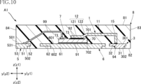
- FIG. 10 is a sectional view taken along line XX in FIG. 1.
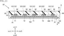
- FIG. 11 is a cross-sectional view taken along line XI-XI in FIG.
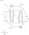
- FIG. 12 is a partially enlarged plan view showing the semiconductor device according to the first embodiment of the present disclosure.
- FIG. 13 is a partially enlarged plan view showing a first modification of the semiconductor device according to the first embodiment of the present disclosure.
- FIG. 14 is a partially enlarged plan view showing a second modification of the semiconductor device according to the first embodiment of the present disclosure.
- FIG. 15 is a partially enlarged plan view showing a third modification of the semiconductor device according to the first embodiment of the present disclosure.
- FIG. 13 is a partially enlarged plan view showing a first modification of the semiconductor device according to the first embodiment of the present disclosure.
- FIG. 14 is a partially enlarged plan view showing a second modification of the semiconductor device according to the first embodiment of the present disclosure
- FIG. 16 is a plan view showing a semiconductor device according to a second embodiment of the present disclosure.
- FIG. 17 is a cross-sectional view taken along line XVII-XVII in FIG. 16.
- FIG. 18 is a cross-sectional view taken along line XVIII-XVIII in FIG. 16.
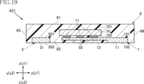
- FIG. 19 is a cross-sectional view showing a first modification of the semiconductor device according to the second embodiment of the present disclosure.
- FIG. 20 is a cross-sectional view showing a second modification of the semiconductor device according to the second embodiment of the present disclosure.
- a thing A is formed on a thing B and "a thing A is formed on a thing B” mean “a thing A is formed on a thing B” unless otherwise specified.
- "something A is placed on something B” and “something A is placed on something B” mean "something A is placed on something B” unless otherwise specified.
- a certain surface A faces (one side or the other side of) the direction B is not limited to the case where the angle of the surface A with respect to the direction B is 90 degrees; Including cases where it is tilted to the opposite direction.
- First embodiment: 1 to 12 show a semiconductor device according to a first embodiment of the present disclosure.
- the semiconductor device A1 of this embodiment includes a plurality of leads 1 to 6, a semiconductor element 7, a wire 99, and a sealing resin 8.
- the semiconductor device A1 is for switching current by being mounted on a substrate, for example, but the specific use of the semiconductor device A1 is not limited in any way.
- the thickness direction of the present disclosure is defined as the thickness direction z.
- One side in the thickness direction z is referred to as the z1 side, and the side opposite to the z1 side in the z direction is referred to as the z2 side.
- one direction perpendicular to the thickness direction z is defined as a first direction x.
- One side in the first direction x is called the x1 side, and the side opposite to the x1 side is called the x2 side.
- a direction perpendicular to the thickness direction z and the first direction x is defined as a second direction y.
- One side in the second direction y is defined as the y1 side
- the side opposite to the y1 side is defined as the y2 side.
- the plurality of leads 1 to 6 are used to appropriately achieve the function of supporting the semiconductor element 7, the function of forming a conductive path to the semiconductor element 7, and the like.
- the plurality of leads 1 to 6 are made of metal such as copper (Cu), nickel (Ni), iron (Fe), or the like.
- the plurality of leads 1 to 6 are formed, for example, by subjecting a metal plate material to a process selected from punching, bending, etching, or the like. Further, a plating layer made of silver (Ag), Ni, gold (Au), etc. may be provided at appropriate locations on each of the plurality of leads 1 to 6, if necessary.
- the plurality of leads 1 to 6 will be described as a first lead 1, a second lead 2, a third lead 3, a fourth lead 4, a fifth lead 5, and an island lead 6. That is, the plurality of leads 1 to 6 include a first lead 1, a second lead 2, a third lead 3, a fourth lead 4, a fifth lead 5, and an island lead 6. Note that, as described later, in this embodiment, the fourth lead 4 and the island lead 6 are connected to each other. Depending on the conduction form of each of the leads 1 to 6, they may be configured as separate pieces, or any of the leads may be connected to each other.
- first lead 1 and the second lead 2 are formed by punching and bending a metal plate material
- third lead 3, fourth lead 4, fifth lead 5, and island lead 6 are formed by punching and bending a metal plate material.
- An example will be explained in which a metal plate material is formed by etching.
- the island lead 6 has a main surface 601, a back surface 602, a thick part 61, a thin part 62, and a plurality of extension parts 63.
- the main surface 601 is a surface facing the z1 side in the z direction, and in the illustrated example, is a smooth surface that is perpendicular to the z direction.
- the island lead 6 may have, for example, a recess or a groove recessed from the main surface 601 as appropriate.
- the back surface 602 is a surface facing the z2 side in the z direction, and faces the opposite side to the main surface 601. In the illustrated example, back surface 602 is a smooth surface that is perpendicular to the z direction.
- a plating layer made of Ni, titanium (Ti), or the like may be provided on the back surface 602 as appropriate.
- the thick portion 61 is a portion where the main surface 601 and the back surface 602 overlap when viewed in the z direction, and in the illustrated example, is a rectangular portion when viewed in the z direction. Note that the shape of the thick portion 61 is not limited at all.
- the thickness of the thick portion 61 in the z direction is the distance between the main surface 601 and the back surface 602.
- the thin portion 62 is a portion that overlaps with the main surface 601 when viewed in the z direction but does not overlap with the back surface 602. In the illustrated example, the thin portion 62 extends from the thick portion 61 to both sides in the x direction and both sides in the y direction when viewed in the z direction. It is connected in such a way that it extends to.
- the thickness of the thin portion 62 in the z direction is smaller than the distance between the main surface 601 and the back surface 602.
- the thickness of the thick portion 61 and the thickness of the thin portion 62 are not limited at all.
- the thickness of the thick portion 61 is approximately 0.2 mm to 0.5 mm
- the thickness of the thin portion 62 is approximately 0.1 mm to 0.4 mm.
- the portion of the thin portion 62 that extends from the thick portion 61 toward the y1 side in the y direction is larger than the portion that extends toward the y2 side.
- the plurality of extending portions 63 are portions extending from the end of the thin wall portion 62. In the illustrated example, the plurality of extending portions 63 extend from the thin portion 62 to both sides in the x direction.
- the number of extension parts 63 is not limited at all, and may be plural or one. In the illustrated example, two extending portions 63 are provided on the x1 side in the x direction, and two extending portions 63 are provided on the x2 side.
- the extending portion 63 has an end surface 631.
- the end surface 631 is a surface facing away from the thin wall portion 62 in the x direction, in other words, a surface facing outward in the x direction.
- the illustrated end surface 631 is a surface perpendicular to the x direction.
- the positions in the x direction of the two end surfaces 631 located on the x1 side in the x direction are the same (or substantially the same). Moreover, the positions in the x direction of the two end surfaces 631 located on the x2 side in the x direction are the same (or substantially the same).
- the first lead 1 As shown in FIGS. 1, 7, and 8 to 12, the first lead 1 is arranged on the z1 side in the z direction relative to the third lead 3, fourth lead 4, fifth lead 5, and island lead 6. ing.
- the first lead 1 of this embodiment includes a first main portion 11 , a plurality of first branch portions 12 , a first extension portion 13 , a third extension portion 14 , and a first standing portion 15 .
- the first main portion 11 is a plate-shaped portion along the xy plane, and in the illustrated example, has a substantially rectangular shape with the x direction as the longitudinal direction.
- the first main portion 11 in the illustrated example has a through hole 111 .
- the through hole 111 penetrates the first main portion 11 in the z direction.
- the number of through holes 111 is not limited, and may be one or more.
- the first main portion 11 has two through holes 111.
- the shape of the through hole 111 is not limited at all, and a circular shape, an elliptical shape, a rectangular shape, a polygonal shape, etc. are appropriately selected.
- the through hole 111 has an elliptical shape with the x direction as the longitudinal direction when viewed in the z direction.
- the plurality of first branch parts 12 extend from the first main part 11 to the y2 side in the y direction.
- the number of first branch parts 12 is not limited at all, and in the illustrated example, three first branch parts 12 are provided.
- the plurality of first branch parts 12 are arranged side by side in the x direction.
- the first branch portion 12 has a first connecting portion 121 and a first root portion 122 .
- the first connecting portion 121 is a portion located on the y2 side in the y direction with respect to the first main portion 11.
- the first connecting portion 121 is located closer to the z2 side than the first main portion 11 in the z direction.
- the shape of the first connecting portion 121 is not limited at all, and in the illustrated example, it has a shape whose longitudinal direction is the y direction when viewed in the z direction.
- the first connection portion 121 is perpendicular to the z direction.
- the first root portion 122 is located between the first connecting portion 121 and the first main portion 11 and is connected to the first connecting portion 121 and the first main portion 11.
- the first root portion 122 approaches the semiconductor element 7 in the z direction (located on the z2 side) as it goes from the first main portion 11 to the first connection portion 121 in the y direction (from the y1 side to the y2 side). is inclined to.
- the three first branch portions 12 include first branch portions 12 that have different lengths in the y direction.
- the first branch 12 located closest to the x2 side in the x direction has a shorter length in the y direction than the other first branches 12.
- the first branch portion 12 located closest to the x2 side in the x direction is located close to a third electrode 73 and a wire 99, which will be described later.
- the plurality of first branch parts 12 may have the same length.
- the first width W11 which is the width in the first direction It is narrower than the second width W12, which is the width in the first direction x.
- the first connecting portion 121 of this example has a shape in which the width in the first direction x decreases from the tip on the y2 side toward the first root portion 122 in the y direction. This first connecting portion 121 is configured only by the first tapered portion of the present disclosure.
- the third width W13 which is the width in the first direction x of the boundary between the first root portion 122 and the first connection portion 121, is smaller than the second width W12.
- the width of the first root portion 122 in the first direction x increases from the first connecting portion 121 side (y2 side) to the first main portion 11 side (y1 side) in the y direction. It has a tapered shape that increases in size.
- the first branch portion 12 in the illustrated example has a tapered shape in which the width in the first direction x increases as it goes from the y2 side to the y1 side in the y direction. That is, the first connecting portion 121 and the first root portion 122 have a continuous tapered shape when viewed in the z direction.
- the first extending portion 13 is a portion extending from the first main portion 11.
- the first extending portion 13 extends from the end of the first main portion 11 on the x1 side in the x direction toward the x1 side.
- the first extending portion 13 has a first end surface 131 .
- the first end surface 131 is a surface facing the opposite side from the first main portion 11 in the x direction, in other words, a surface facing the x1 side which is the outside in the x direction.
- the illustrated first end surface 131 is a surface perpendicular to the x direction.
- the position of the first end surface 131 in the x direction is the same (or substantially the same) as the position in the x direction of the plurality of end surfaces 631 located on the x1 side in the x direction.
- the third extending portion 14 is a portion extending from the first main portion 11.
- the third extending portion 14 extends from the end of the first main portion 11 on the x2 side in the x direction toward the x2 side.
- the third extending portion 14 has a third end surface 141.
- the third end surface 141 is a surface facing the opposite side from the first main portion 11 in the x direction, in other words, a surface facing the x2 side which is the outside in the x direction.
- the illustrated third end surface 141 is a surface perpendicular to the x direction. Further, the position of the third end surface 141 in the x direction is the same (or substantially the same) as the position in the x direction of the plurality of end surfaces 631 located on the x2 side in the x direction.
- the first standing portion 15 is connected to an end portion of the first main portion 11 on the y1 side in the y direction, which is opposite to the first branch portion 12.
- the first upright portion 15 extends from the first main portion 11 toward the z2 side in the z direction.
- the shape of the first upright portion 15 is not limited in any way, and in the illustrated example, it has a rectangular shape with the x direction as the longitudinal direction. In the illustrated example, the center of the first upright portion 15 in the x direction is the same (or substantially the same) as the center of the first main portion 11 in the x direction.
- the z2 side tip of the first upright portion 15 of the first lead 1 in the z direction is electrically connected to the third lead 3 via the fourth conductive joint 94.
- the fourth conductive joint 94 is made of, for example, solder, Ag paste material, Ag sintered material, Cu sintered material, or the like.
- 2nd lead 2 As shown in FIGS. 1, 7, and 8 to 12, the second lead 2 is arranged on the z1 side in the z direction relative to the third lead 3, fourth lead 4, fifth lead 5, and island lead 6. ing. Further, the second lead 2 is arranged on the y2 side in the y direction with respect to the first lead 1.
- the second lead 2 of this embodiment includes a second main portion 21, a plurality of second branch portions 22, a second extension portion 23, a fourth extension portion 24, a second upright portion 25, and a connecting portion 29. are doing.
- the second main portion 21 is a plate-shaped portion along the xy plane, and in the illustrated example, has a substantially rectangular shape with the x direction as the longitudinal direction.
- the first main portion 11 and the second main portion 21 are arranged on opposite sides of each other in the y direction with the semiconductor element 7 as a reference.
- the second main portion 21 in the illustrated example has a through hole 211 .
- the through hole 211 penetrates the second main portion 21 in the z direction.
- the number of through holes 211 is not limited, and may be one or more.
- the second main portion 21 has two through holes 211 .
- the shape of the through hole 211 is not limited at all, and a circular shape, an elliptical shape, a rectangular shape, a polygonal shape, etc.
- the through hole 211 has an elliptical shape with the x direction as the longitudinal direction when viewed in the z direction.
- the second main part 21 is arranged at the same (or substantially the same) position as the first main part 11 in the z direction.
- the plurality of second branch portions 22 extend from the second main portion 21 toward the y1 side in the y direction.
- the number of second branch parts 22 is not limited at all, and in the illustrated example, two second branch parts 22 are provided.
- the plurality of second branch parts 22 are arranged side by side in the x direction.
- the second branch portion 22 has a second connecting portion 221 and a second root portion 222 .
- the second connecting portion 221 is a portion located on the y1 side in the y direction with respect to the second main portion 21.
- the second connecting portion 221 is located closer to the z2 side than the second main portion 21 in the z direction.
- the shape of the second connecting portion 221 is not limited at all, and in the illustrated example, it has a shape whose longitudinal direction is the y direction when viewed in the z direction.
- the second connection portion 221 is perpendicular to the z direction.
- the second root portion 222 is located between the second connection portion 221 and the second main portion 21 and is connected to the second connection portion 221 and the second main portion 21 .
- the second root portion 222 approaches the semiconductor element 7 in the z direction (located on the z2 side) as it goes from the second main portion 21 to the second connection portion 221 in the y direction (as it goes from the y2 side to the y1 side). is inclined to.
- the lengths of the two second branch portions 22 in the y direction are equal.
- the plurality of second branch portions 22 may have different lengths in the y direction.
- the fourth width W21 which is the width in the first direction It is narrower than the fifth width W22, which is the width in the first direction x.
- the second connecting portion 221 of this example has a shape in which the width in the first direction x decreases from the tip on the y1 side toward the second root portion 222 in the y direction. This second connecting portion 221 is configured only by the second tapered portion of the present disclosure.
- the sixth width W23 which is the width in the first direction x of the boundary between the second root portion 222 and the second connecting portion 221, is smaller than the fifth width W22.
- the width of the second root portion 222 in the first direction x increases from the second connecting portion 221 side (y1 side) to the second main portion 21 side (y2 side) in the y direction. It has a tapered shape that increases in size.
- the second branch portion 22 in the illustrated example has a tapered shape in which the width in the first direction x increases as it goes from the y1 side to the y2 side in the y direction. That is, the second connecting portion 221 and the second root portion 222 have a continuous tapered shape when viewed in the z direction.
- the second extending portion 23 is a portion extending from the second main portion 21.
- the second extending portion 23 extends from the end of the second main portion 21 on the x1 side in the x direction toward the x1 side.
- the second extending portion 23 has a second end surface 231 .
- the second end surface 231 is a surface facing the opposite side from the second main portion 21 in the x direction, in other words, a surface facing the x1 side which is the outside in the x direction.
- the illustrated second end surface 231 is a surface perpendicular to the x direction.
- the position of the second end surface 231 in the x direction is the same (or substantially the same) as the first end surface 131 and the end surface 631 located on the x1 side in the x direction.
- the fourth extending portion 24 is connected to the second main portion 21 via a connecting portion 29.
- the connecting portion 29 has a smaller dimension in the y direction than the second main portion 21 and the fourth extending portion 24 .
- the fourth extending portion 24 in the present disclosure is not limited to a configuration in which it is directly connected to the second main portion 21, but includes a configuration in which it is connected to the second main portion 21 via another portion. The same applies to the second extending portion 23 in this respect.
- the above-mentioned first extension part 13 and third extension part 14 are not limited to a structure in which they are directly connected to the first main part 11, but are also in a structure in which they are connected to the first main part 11 through other parts. including.
- the fourth extending portion 24 extends along the y direction.
- the fourth extending portion 24 has a fourth end surface 241 .
- the fourth end surface 241 is a surface facing opposite to the second main portion 21 in the y direction, in other words, a surface facing the y2 side, which is the outside in the y direction.
- the illustrated fourth end surface 241 is a surface perpendicular to the y direction.
- the second upright portion 25 is connected to the end of the second main portion 21 on the y2 side in the y direction, which is opposite to the second branch portion 22.
- the second upright portion 25 extends from the second main portion 21 toward the z2 side in the z direction.
- the shape of the second upright portion 25 is not limited at all, and in the illustrated example, it has a rectangular shape with the x direction as the longitudinal direction. In the illustrated example, the center of the second upright portion 25 in the x direction is the same (or substantially the same) as the center of the second main portion 21 in the x direction.
- the tip of the second upright portion 25 of the second lead 2 on the z2 side in the z direction is electrically connected to the fourth lead 4 via the fifth conductive joint 95.
- the fifth conductive joint 95 is, for example, solder.
- the third lead 3 is arranged apart from the island lead 6 on the y1 side in the y direction.
- the center of the third lead 3 in the x direction is the same (or substantially the same) as the center of the island lead 6 in the x direction.
- the third lead 3 has a main surface 301, a back surface 302, a thick part 31, a thin part 32, and a plurality of extension parts 33.
- the main surface 301 is a surface facing the z1 side in the z direction, and in the illustrated example, is a smooth surface that is perpendicular to the z direction.
- the third lead 3 may have, for example, a recess or a groove recessed from the main surface 301 as appropriate.
- the first upright portion 15 described above is joined to the main surface 301 via the fourth conductive joint 94 .
- the back surface 302 is a surface facing the z2 side in the z direction, and faces the opposite side to the main surface 301.
- back surface 302 is a smooth surface that is perpendicular to the z direction.
- a plating layer made of Ni, Ti, etc. may be provided on the back surface 302 as appropriate.
- the main surface 301 is at the same (or substantially the same) position as the main surface 601 in the z direction
- the back surface 302 is at the same (or substantially the same) position as the back surface 602.
- the thick portion 31 is a portion where the main surface 301 and the back surface 302 overlap when viewed in the z direction.
- the thick portion 31 is a rectangular portion whose longitudinal direction is the x direction when viewed in the z direction. Note that the shape of the thick portion 31 is not limited at all.
- the thickness of the thick portion 31 in the z direction is the distance between the main surface 301 and the back surface 302.
- the thin portion 32 is a portion that overlaps the main surface 301 and does not overlap the back surface 302 when viewed in the z direction.
- the thin portion 32 is connected to the thick portion 31 so as to extend from the thick portion 31 to both sides in the x direction and to the y2 side in the y direction.
- the thin portion 32 has a portion connected to the thick portion 31 so as to extend toward the y1 side in the y direction when viewed in the z direction, and this portion is sandwiched between the extending portions 33 in the x direction.
- the thickness of the thin portion 32 in the z direction is smaller than the distance between the main surface 301 and the back surface 302.
- the thickness of the thick portion 31 and the thickness of the thin portion 32 are not limited at all. In this embodiment, the thickness of the thick portion 31 is the same (or approximately the same) as the thickness of the thick portion 61, and the thickness of the thin portion 32 is the same (or approximately the same) as the thickness of the thin portion 62. ).
- the plurality of extending portions 33 are portions extending from the end of the thick portion 31. In the illustrated example, the plurality of extending portions 33 extend from the thick portion 31 toward the y1 side in the y direction.
- the number of extension parts 33 is not limited at all, and may be plural or one. In the illustrated example, four extensions 33 are provided.
- the extending portion 33 has an end surface 331.
- the end surface 331 is a surface facing the opposite side from the thick portion 31 in the y direction, in other words, a surface facing the y1 side, which is the outside in the y direction.
- the illustrated end surface 331 is a surface perpendicular to the y direction. The positions of the plurality of end surfaces 331 in the y direction are the same (or substantially the same).
- the fourth lead 4 is arranged on the y2 side of the island lead 6 in the y direction. Further, the center of the fourth lead 4 in the x direction is located on the x1 side in the x direction from the center of the island lead 6 in the x direction. In the semiconductor device A1, the fourth lead 4 and the island lead 6 are connected by a relay portion 49. Unlike this configuration, the fourth lead 4 may be separated from the island lead 6. As shown in FIGS. 1 to 3 and 8 to 10, the fourth lead 4 has a main surface 401, a back surface 402, a thick part 41, a thin part 42, and a plurality of extension parts 43.
- the main surface 401 is a surface facing the z1 side in the z direction, and in the illustrated example, is a smooth surface that is perpendicular to the z direction.
- the fourth lead 4 may have, for example, a recess or a groove recessed from the main surface 401 as appropriate.
- the aforementioned second standing portion 25 is joined to the main surface 401 via the fifth conductive joining portion 95 .
- the back surface 402 is a surface facing the z2 side in the z direction, and faces the opposite side to the main surface 401.
- back surface 402 is a smooth surface that is perpendicular to the z direction.
- a plating layer made of Ni, Ti, etc. may be provided on the back surface 402 as appropriate.
- the main surface 401 is at the same (or substantially the same) position as the main surface 601 in the z direction
- the back surface 402 is at the same (or substantially the same) position as the back surface 602.
- the thick portion 41 is a portion where the main surface 401 and the back surface 402 overlap when viewed in the z direction.
- the thick portion 41 is a rectangular portion whose longitudinal direction is the x direction when viewed in the z direction. Note that the shape of the thick portion 41 is not limited at all.
- the thickness of the thick portion 41 in the z direction is the distance between the main surface 401 and the back surface 402. In this embodiment, the dimension of the thick portion 41 in the x direction is smaller than the dimension of the thick portion 31 in the x direction.
- the thin portion 42 is a portion that overlaps the main surface 401 and does not overlap the back surface 402 when viewed in the z direction.
- the thin portion 42 is connected to the thick portion 41 so as to extend from the thick portion 41 to both sides in the x direction and to the y1 side in the y direction. Further, the thin wall portion 42 has a portion extending from the thick wall portion 41 toward the y2 side in the y direction when viewed in the z direction, and this portion is sandwiched between the extending portions 43 in the x direction.
- the thickness of the thin portion 42 in the z direction is smaller than the distance between the main surface 401 and the back surface 402.
- the thickness of the thick portion 41 and the thickness of the thin portion 42 are not limited at all. In this embodiment, the thickness of the thick portion 41 is the same (or approximately the same) as the thickness of the thick portion 61, and the thickness of the thin portion 42 is the same (or approximately the same) as the thickness of the thin portion 62. ).
- the plurality of extending portions 43 are portions extending from the end of the thick portion 41.
- the plurality of extending portions 43 extend from the thick portion 41 toward the y2 side in the y direction.
- the number of extension parts 43 is not limited at all, and may be plural or one.
- three extensions 43 are provided. The positions of these three extensions 43 in the x direction are the same (or approximately the same) as the positions in the x direction of the three extensions 33 located on the x1 side in the x direction among the plurality of extensions 33. .
- the extending portion 43 has an end surface 431.
- the end surface 431 is a surface facing away from the thick portion 41 in the y direction, in other words, a surface facing the y2 side, which is the outside in the y direction.
- the illustrated end surface 431 is a surface perpendicular to the y direction.
- the positions of the plurality of end surfaces 431 in the y direction are the same (or substantially the same). Further, the positions of the plurality of end surfaces 431 in the y direction are the same (or substantially the same) as the fourth end surface 241.
- the fifth lead 5 is arranged on the y2 side of the island lead 6 in the y direction. Further, the center of the fifth lead 5 in the x direction is located on the x2 side in the x direction from the center of the island lead 6 in the x direction. The fifth lead 5 is arranged on the x2 side in the x direction with respect to the fourth lead 4. As shown in FIGS. 1 to 3 and FIG. 10, the fifth lead 5 has a main surface 501, a back surface 502, a thick portion 51, a thin portion 52, and an extending portion 53.
- the main surface 501 is a surface facing the z1 side in the z direction, and in the illustrated example, is a smooth surface that is perpendicular to the z direction.
- the fifth lead 5 may have, for example, a recess or a groove recessed from the main surface 501 as appropriate.
- a wire 99 is bonded to the main surface 501 .
- the back surface 502 is a surface facing the z2 side in the z direction, and faces the opposite side to the main surface 501.
- back surface 502 is a smooth surface that is perpendicular to the z direction.
- a plating layer made of Ni, Ti, etc. may be provided on the back surface 502 as appropriate.
- the main surface 501 is at the same (or substantially the same) position as the main surface 601 in the z direction
- the back surface 502 is at the same (or substantially the same) position as the back surface 602.
- the thick portion 51 is a portion where the main surface 501 and the back surface 502 overlap when viewed in the z direction.
- the thick portion 51 is a rectangular portion when viewed in the z direction.
- the shape of the thick portion 51 is not limited at all.
- the thickness of the thick portion 51 in the z direction is the distance between the main surface 501 and the back surface 502.
- the dimension of the thick portion 51 in the x direction is smaller than the dimension of the thick portion 31 and the thick portion 41 in the x direction.
- the thin portion 32 is a portion that overlaps the main surface 301 and does not overlap the back surface 302 when viewed in the z direction.
- the thin portion 32 is connected to the thick portion 51 so as to extend from the thick portion 51 to both sides in the x direction and to the y1 side in the y direction.
- the thickness of the thin portion 52 in the z direction is smaller than the distance between the main surface 501 and the back surface 502.
- the thickness of the thick portion 51 and the thickness of the thin portion 52 are not limited at all. In this embodiment, the thickness of the thick portion 51 is the same (or approximately the same) as the thickness of the thick portion 61, and the thickness of the thin portion 52 is the same (or approximately the same) as the thickness of the thin portion 62. ).
- the extending portion 53 is a portion extending from the end of the thick portion 51. In the illustrated example, the extending portion 53 extends from the thick portion 51 toward the y2 side in the y direction.
- the number of extension parts 53 is not limited at all, and may be plural or one. In the illustrated example, one extension 53 is provided.
- the position of the extension part 53 in the x direction is the same (or substantially the same) as the position in the x direction of the extension part 33 located closest to the x2 side in the x direction among the plurality of extension parts 33.
- the extending portion 53 has an end surface 531.
- the end surface 531 is a surface facing opposite to the thick portion 51 in the y direction, in other words, a surface facing the y2 side, which is the outside in the y direction.
- the illustrated end surface 531 is a surface perpendicular to the y direction. Further, the position of the end surface 531 in the y direction is the same (or substantially the same) as the fourth end surface 241 and the plurality of end surfaces 431.
- the semiconductor element 7 is an element that performs the electrical functions of the semiconductor device A1.
- the specific configuration of the semiconductor element 7 is not limited at all, and in this embodiment, the semiconductor element 7 is a transistor using a nitride semiconductor, and more specifically, a GaN-transistor using gallium nitride (GaN). It is a HEMT (High Electron Mobility Transistor) element.
- the semiconductor element 7 is not limited to one using a nitride semiconductor, and may also use other semiconductors such as silicon (Si) and silicon carbide (SiC).
- the semiconductor element 7 is not limited to a HEMT, and may be other transistors such as a MOSFET (Metal-Oxide-Semiconductor Field Effect Transistor) and an IGBT (Insulated Gate Bipolar Transistor).
- MOSFET Metal-Oxide-Semiconductor Field Effect Transistor
- IGBT Insulated Gate Bipolar Transistor
- the semiconductor element 7 is mounted on the thick portion 61 of the island lead 6. As shown in FIGS. 1, 2, and 8 to 12, the semiconductor element 7 includes an element body 70, a plurality of first electrodes 71, a plurality of second electrodes 72, and a third electrode 73.
- the element body 70 is, for example, a portion in which a substrate layer, a buffer layer, and a nitride layer (all not shown) are laminated.
- the element body 70 has an element main surface 701 and an element back surface 702.
- the element main surface 701 is a surface facing the z1 side in the z direction.
- the element back surface 702 is a surface facing the z2 side in the z direction, and faces the opposite side to the element main surface 701.
- the back surface 702 of the element is provided with a metal layer. As shown in FIGS. 12 to 14, this metal layer and the main surface 601 of the island lead 6 are joined by a first conductive joint 91. As shown in FIGS.
- the first conductive joint 91 is made of, for example, solder, Ag paste material, Ag sintered material, Cu sintered material, or the like.
- the above-described metal layer is provided for bonding by the first conductive bonding portion 91, a configuration may be adopted in which the metal layer is not provided.
- the metal layer may have the same potential as, for example, the second electrode 72 and the like.
- the semiconductor element 7 is disposed at a position overlapping a portion of the thick portion 61 and a portion of the thin portion 62 of the island lead 6 when viewed in the z direction.
- a plurality of first electrodes 71, a plurality of second electrodes 72, and a third electrode 73 are arranged on the element main surface 701.
- the numbers of the plurality of first electrodes 71 and the plurality of second electrodes 72 are not limited at all. In the illustrated example, three first electrodes 71 and two second electrodes 72 are provided.
- the number of the plurality of first electrodes 71 and the number of the plurality of first branch parts 12 are the same, and the number of the plurality of second electrodes 72 and the number of the plurality of second branch parts 22 are the same.
- the first electrode 71 is an electrode that functions as a drain electrode.
- the second electrode 72 is an electrode that functions as a source electrode.
- the plurality of first electrodes 71 and the plurality of second electrodes 72 are arranged alternately in the x direction.
- the shapes of the first electrode 71 and the second electrode 72 are not limited at all, and in the illustrated example, they have a shape whose longitudinal direction is in the y direction, and more specifically, a tapered shape.
- FIG. 1, FIG. 2, FIG. 8, and FIGS. They are individually electrically connected via conductive joints 92 .
- the second conductive joint 92 is made of, for example, solder, Ag paste material, Ag sintered material, Cu sintered material, or the like.
- FIG. 1, FIG. 2, FIG. 9, FIG. 11, and FIG. They are individually electrically connected via conductive joints 93.
- the third conductive joint 93 is made of, for example, solder, Ag paste material, Ag sintered material, Cu sintered material, or the like.
- the third electrode 73 is an electrode that functions as a gate electrode.
- the number of third electrodes 73 is not limited, and may be one or more. In the illustrated example, one third electrode 73 is provided.
- the third electrode 73 is arranged, for example, at one of the four corners of the element main surface 701, and in the illustrated example, it is arranged near the corner of the element main surface 701 on the x2 side in the x direction and the y2 side in the y direction. has been done. Further, the third electrode 73 is arranged on the y2 side in the y direction with respect to the first electrode 71 on the x2 side in the x direction of the two first electrodes 71.
- a wire 99 is connected to the third electrode 73 and electrically connected to the fifth lead 5 via the wire 99. Note that instead of the wire 99, a conductive member made of a metal plate material may be used to conduct the third electrode 73 and the fifth lead 5.
- the sealing resin 8 covers a portion of each of the plurality of leads 1 to 6, the semiconductor element 7, and the wire 99, and is made of an insulating material such as epoxy resin. As shown in FIGS. 1 to 11, the sealing resin 8 has a first surface 81, a second surface 82, a third surface 83, a fourth surface 84, a fifth surface 85, and a sixth surface 86. , has a rectangular parallelepiped shape.
- the first surface 81 is a surface facing the z1 side in the z direction. In the illustrated example, the first surface 81 is a plane perpendicular to the z direction.
- the second surface 82 is a surface facing the z2 side in the z direction. In the illustrated example, the second surface 82 is a plane perpendicular to the z direction.
- the third surface 83 is a surface facing the y1 side in the y direction. In the illustrated example, the third surface 83 is a plane perpendicular to the y direction.
- the fourth surface 84 is a surface facing the y2 side in the y direction. In the illustrated example, the fourth surface 84 is a plane perpendicular to the y direction.
- the fifth surface 85 is a surface facing the x1 side in the x direction. In the illustrated example, the fifth surface 85 is a plane perpendicular to the x direction.
- the sixth surface 86 is a surface facing the x2 side in the x direction. In the illustrated example, the sixth surface 86 is a plane perpendicular to the x direction.
- the back surface 602 of the island lead 6, the back surface 302 of the third lead 3, the back surface 402 of the fourth lead 4, and the back surface 502 of the fifth lead 5 are exposed on the z2 side in the z direction.
- the second surface 82, the back surface 602 of the island lead 6, the back surface 302 of the third lead 3, the back surface 402 of the fourth lead 4, and the back surface 502 of the fifth lead 5 are flush with each other.
- all or any of the back surface 602 of the island lead 6, the back surface 302 of the third lead 3, the back surface 402 of the fourth lead 4, and the back surface 502 of the fifth lead 5 may protrude slightly from the second surface 82. good.
- a plurality of end surfaces 331 of the third lead 3 are exposed on the y1 side in the y direction.
- the third surface 83 and the plurality of end surfaces 331 of the third lead 3 are flush with each other. However, all or any of the plurality of end surfaces 331 may slightly protrude from the third surface 83.
- the fourth end surface 241 of the second lead 2, the plurality of end surfaces 431 of the fourth lead 4, and the end surface 531 of the fifth lead 5 are exposed on the y2 side in the y direction.
- the fourth surface 84, the fourth end surface 241 of the second lead 2, the plurality of end surfaces 431 of the fourth lead 4, and the end surface 531 of the fifth lead 5 are flush with each other.
- all or any of the fourth end surface 241 of the second lead 2, the plurality of end surfaces 431 of the fourth lead 4, and the end surface 531 of the fifth lead 5 may protrude slightly from the fourth surface 84.
- the first end surface 131 of the first lead 1, the second end surface 231 of the second lead 2, and the plurality of end surfaces 631 of the island lead 6 are exposed on the x1 side in the x direction.
- the fifth surface 85, the first end surface 131 of the first lead 1, the second end surface 231 of the second lead 2, and the plurality of end surfaces 631 of the island lead 6 are flush with each other. However, all or any of the first end surface 131 of the first lead 1, the second end surface 231 of the second lead 2, and the plurality of end surfaces 631 of the island lead 6 may protrude slightly from the fifth surface 85.
- the third end surface 141 of the first lead 1 and the plurality of end surfaces 631 of the island leads 6 are exposed on the x2 side in the x direction.
- the sixth surface 86, the third end surface 141 of the first lead 1, and the plurality of end surfaces 631 of the island lead 6 are flush with each other.
- all or any of the third end surface 141 of the first lead 1 and the plurality of end surfaces 631 of the island lead 6 may protrude slightly from the sixth surface 86.
- the semiconductor device A1 is mounted on a circuit board (not shown) or the like using the back surface 302, back surface 402, and back surface 502 exposed from the second surface 82 of the sealing resin 8 as mounting terminals. That is, in the semiconductor device A1, the mounting surface is the z2 side opposite to the z1 side, which is the side toward which the element main surface 701 of the semiconductor element 7 faces in the z direction. Further, the back surface 602 is used as a heat dissipation surface for dissipating heat from the semiconductor element 7.
- the first width W11 of the first branch portion 12 is narrower than the second width W12.
- the first connecting portion 121 is electrically connected to the first electrode 71 . Therefore, a current flows in the first branch portion 12 in the y direction. This current increases toward the first main portion 11 in the y direction.
- the first branch portion 12, which is a current conduction path, has a larger width on the side where the first main portion 11 is located in the y direction. Therefore, current concentration on the current path can be alleviated.
- the first branch portion 12 is in a cantilevered state with one side supported by the first main portion 11.
- the tip of the first branch part 12 is positioned on the z2 side in the thickness direction z.
- the entire first branch portion 12 may bend.
- the second width W12 is larger than the first width W11, it is possible to suppress the bending of the first branch portion 12, and it is possible to more appropriately manufacture the semiconductor device A1. .
- the first connecting portion 121 has a tapered shape in which the width in the first direction x increases toward the first root portion 122 in the y direction. Such a shape is preferable for alleviating current concentration. Further, in this example, the entire first connecting portion 121 has a tapered shape. Such a configuration is preferable because it alleviates current concentration.
- the first root portion 122 has a tapered shape. This can further promote mitigation of current concentration and suppression of deflection.
- the fourth width W21 of the second branch portion 22 is narrower than the fifth width W22.
- the second connection portion 221 is electrically connected to the second electrode 72 . Therefore, a current flows in the second branch portion 22 in the y direction. This current increases toward the first main portion 11 in the y direction.
- the second branch portion 22, which is the current conduction path has a larger width on the side where the first main portion 11 is located in the y direction. Therefore, current concentration on the current path can be alleviated.
- the second branch portion 22 is in a cantilevered state with one side supported by the first main portion 11.
- the tip of the second branch portion 22 is positioned on the z2 side in the thickness direction z.
- the entire second branch portion 22 may bend.
- the fifth width W22 is larger than the fourth width W21, it is possible to suppress the bending of the second branch portion 22, and the semiconductor device A1 can be manufactured more appropriately. .
- the second connecting portion 221 has a tapered shape in which the width in the first direction x increases toward the first root portion 122 in the y direction. Such a shape is preferable for alleviating current concentration. Further, in this example, the entire second connecting portion 221 has a tapered shape. Such a configuration is preferable because it alleviates current concentration.
- first root portion 122 has a tapered shape. This can further promote mitigation of current concentration and suppression of deflection.
- FIG. 13 shows a first modification of the semiconductor device A1.
- the configurations of the first branch portion 12 and the second branch portion 22 are different from the semiconductor device A1.
- the second width W12 and the third width W13 of the first branch portion 12 are equal. That is, the first root portion 122 has a shape with a constant width in the first direction x. Further, the fifth width W22 and the sixth width W23 of the second branch portion 22 are equal. That is, the second root portion 222 has a shape with a constant width in the first direction x.
- the first branch portion 12 and the first extension portion 13 are not limited to a tapered configuration as a whole.
- FIG. 14 shows a second modification of the semiconductor device A1.
- the configurations of the first branch portion 12 and the second branch portion 22 are different from those of the above-mentioned example.
- first root portion 122 and the second root portion 222 both have a shape with a constant width in the first direction x.
- the first connecting portion 121 includes a first tapered portion 1211 and a first equal width portion 1212.
- the first tapered portion 1211 has a shape in which the width in the first direction x increases from the tip on the y2 side toward the first root portion 122 side (y1 side).
- the first equal width portion 1212 is interposed between the first tapered portion 1211 and the first root portion 122.
- the first equal width portion 1212 has a constant width in the first direction x. In the illustrated example, the width of the first equal width portion 1212 in the first direction x is the same as (or approximately equal to) the width of the first root portion 122 in the first direction same).
- the first length L11 which is the length of the first tapered part 1211 in the y direction, is longer than the second length L12, which is the length of the first equal width part 1212 in the y direction.
- the second connecting portion 221 includes a second tapered portion 2211 and a second equal width portion 2212.
- the second tapered portion 2211 has a shape in which the width in the first direction x increases from the tip on the y1 side toward the second root portion 222 side (y2 side).
- the second equal width portion 2212 is interposed between the second tapered portion 2211 and the second root portion 222.
- the second equal width portion 2212 has a constant width in the first direction x.
- the width of the second equal width portion 2212 in the first direction x is the same as (or approximately) the width of the second root portion 222 in the first direction same).
- the third length L21 which is the length of the second tapered portion 2211 in the y direction, is longer than the fourth length L22, which is the length of the second equal width portion 2212 in the y direction.
- the first connecting portion 121 and the first root portion 122 are not limited to a configuration consisting only of a tapered portion.
- FIG. 15 shows a third modification of the semiconductor device A1.
- the configurations of the first branch portion 12 and the second branch portion 22 are different from those of the above-mentioned example.
- the first root portion 122 of this modification includes a first wide portion 1221 and a second narrow portion 1222.
- the first wide portion 1221 has a larger width in the first direction x than the second narrow portion 1222 and is interposed between the second narrow portion 1222 and the first main portion 11 .
- the second narrow portion 1222 is interposed between the first wide portion 1221 and the first connecting portion 121 .
- the width of the first wide portion 1221 in the first direction x is the second width W12
- the width of the second narrow portion 1222 in the first direction x is the third width W13. There is.
- the first wide portion 1221 does not overlap the first electrode 71 when viewed in the thickness direction z.
- the second root portion 222 of this modification includes a first wide portion 2221 and a second narrow portion 2222.
- the first wide portion 2221 has a larger width in the first direction x than the second narrow portion 2222 and is interposed between the second narrow portion 2222 and the second main portion 21 .
- the second narrow portion 2222 is interposed between the first wide portion 2221 and the second connecting portion 221.
- the width of the first wide portion 2221 in the first direction x is the fifth width W22
- the width of the second narrow portion 2222 in the first direction x is the sixth width W23.
- the first wide portion 2221 does not overlap the second electrode 72 when viewed in the thickness direction z.
- the shapes of the first root portion 122 and the second root portion 222 are not limited at all.
- the first wide part 1221 does not overlap with the first electrode 71 and the first wide part 2221 does not overlap with the second electrode 72 when viewed in the thickness direction z, the first wide part 1221 and the first wide part 1221 do not overlap with the second electrode 72. Insulation between the first electrode 71 and the first wide portion 2221 and the second electrode 72 can be more reliably ensured.
- Second embodiment 16 to 18 show a semiconductor device according to a second embodiment of the present disclosure.
- the semiconductor device A2 of this embodiment includes a first lead 1, a second lead 2, a fifth lead 5, a semiconductor element 7, and a sealing resin 8.
- the semiconductor element 7 of this embodiment is arranged with the element main surface 701 facing the z2 side in the z direction and the element back surface 702 facing the z1 side in the z direction.
- the plurality of first electrodes 71, the plurality of second electrodes 72, and the third electrodes 73 are constituted by a plurality of metal bumps.
- the plurality of first electrodes 71 are made up of a plurality of metal bumps (two or three in the figure) arranged in the y direction.
- a plurality of sets (three sets) of first electrodes 71 are arranged in the first direction x.
- the plurality of second electrodes 72 are made up of a plurality of metal bumps (three in the figure) arranged in the y direction.
- a plurality of sets (two sets) of second electrodes 72 are arranged in the first direction x.
- the plurality of sets of first electrodes 71 and the plurality of sets of second electrodes 72 are arranged alternately in the first direction x.
- the first lead 1 has a main surface 101 and a back surface 102.
- the main surface 101 is a surface facing the z1 side in the z direction, and faces the element main surface 701 of the semiconductor element 7 .
- the back surface 102 is a surface facing the z2 side in the z direction, and is exposed from the second surface 82 of the sealing resin 8.
- the thickness of the first lead 1 in the z direction is constant.
- the second lead 2 has a main surface 201 and a back surface 202.
- the main surface 201 is a surface facing the z1 side in the z direction, and faces the element main surface 701 of the semiconductor element 7 .
- the back surface 202 is a surface facing the z2 side in the z direction, and is exposed from the second surface 82 of the sealing resin 8.
- the thickness of the second lead 2 in the z direction is constant.
- the shapes of the plurality of first branch portions 12 of the first lead 1 and the plurality of second branch portions 22 of the second lead 2 when viewed in the z direction are, for example, similar to the plurality of first branch portions 12 and the plurality of second branch portions 22 of the semiconductor device A1 described above. This is similar to the second branch 22 of.
- the plurality of first branch parts 12 and the plurality of second branch parts 22 may have the shapes in the semiconductor devices A11, A12, A13, or may have other shapes.
- the plurality of first branch parts 12 and the plurality of second branch parts 22 are located on the z2 side in the z direction with respect to the semiconductor element 7.
- the plurality of first branch parts 12 are individually electrically connected to the plurality of sets of first electrodes 71 via second conductive joints 92.
- the plurality of second branch parts 22 are electrically connected to the plurality of sets of second electrodes 72 via third conductive joints 93.
- the fifth lead 5 has a third connecting portion 55.
- a third electrode 73 is electrically connected to the third connection portion 55 by a conductive connection portion (not shown).
- One surface of the fifth lead 5 is exposed from the second surface 82 of the sealing resin 8.
- the semiconductor device A2 of this embodiment has a structure in which the semiconductor element 7 is flip-chip bonded to the first lead 1, the second lead 2, and the third lead 3.
- the back surface 102 of the first lead 1, the back surface 202 of the second lead 2, and one surface (the surface exposed from the second surface 82) of the fifth lead 5 are used when the semiconductor device A2 is mounted on a circuit board (not shown) or the like. It is used as a mounting terminal when mounting.
- the bonding form between the first lead 1 and the second lead 2 and the semiconductor element 7 is not limited at all.
- FIG. 19 shows a first modification of the semiconductor device A2.
- the first branch portion 12 of the first lead 1 is thinner than the first main portion 11.
- the first branch portion 12 is not exposed from the second surface 82 of the sealing resin 8 to the z2 side in the z direction.
- the second branch portion 22 of the second lead 2 is thinner than the second main portion 21 .
- the second branch portion 22 is not exposed from the second surface 82 of the sealing resin 8 to the z2 side in the z direction.
- Such first leads 1 and second leads 2 can be formed, for example, by etching a metal plate material from both sides in the z direction.
- the first lead 1 and the second lead 2 may have a configuration in which the thickness is not constant.
- FIG. 20 shows a second modification of the semiconductor device A2.
- the semiconductor device A22 of this modification has a configuration in which the first branch portion 12 of the first lead 1 is located closer to the z1 side than the first main portion 11 in the z direction.
- the first branch portion 12 is not exposed from the second surface 82 of the sealing resin 8 to the z2 side in the z direction.
- the first main portion 11 and the first branch portion 12 have the same (or substantially the same) thickness in the thickness direction z.
- the second branch portion 22 is located closer to the z1 side in the z direction than the second main portion 21.
- the second branch portion 22 is not exposed from the second surface 82 of the sealing resin 8 to the z2 side in the z direction.
- the second main portion 21 and the second branch portion 22 have the same (or substantially the same) thickness in the thickness direction z.
- Such first and second leads 2 can be formed, for example, by bending a metal plate material.
- the first lead 1 and the second lead 2 may be bent in the thickness direction z.
- the semiconductor device according to the present disclosure is not limited to the embodiments described above.
- the specific configuration of each part of the semiconductor device according to the present disclosure can be changed in design in various ways.
- the present disclosure includes the embodiments described in the appendix below.
- the plurality of leads include a first lead
- the semiconductor element includes a main surface of the device facing one side in the thickness direction, a back surface of the device facing the other side, and a plurality of first electrodes arranged along a first direction intersecting the thickness direction on the main surface of the device.
- the first lead includes a first main portion and a plurality of first leads extending from the first main portion in the thickness direction and a second direction intersecting the first direction, and arranged along the first direction.
- the first branch portion has a first root portion connected to the first main portion, and a first connection portion electrically connected to the first electrode, A first width, which is a width in the first direction, of a tip of the first connecting portion is narrower than a second width, which is a width in the first direction, of a boundary between the first root portion and the first main portion.
- semiconductor devices Appendix 2. The semiconductor device according to appendix 1, wherein the first connection portion includes a first tapered portion whose width in the first direction increases from the tip toward the first root. Appendix 3. The semiconductor device according to appendix 2, wherein the first connection portion includes only the first tapered portion. Appendix 4.
- the semiconductor device wherein the first connection portion includes a first equal width portion interposed between the first tapered portion and the first root portion.
- Appendix 5 The semiconductor according to appendix 4, wherein a first length of the first tapered portion in the second direction is longer than a second length of the first uniform width portion in the second direction.
- Device. Appendix 6.
- Appendix 7. The semiconductor according to supplementary note 1, wherein a third width, which is a width in the first direction of a boundary between the first root portion and the first connection portion, is smaller than the second width and larger than the first width.
- the first root portion includes a first wide portion and a first narrow portion
- the plurality of leads include a second lead,
- the semiconductor element includes a plurality of second electrodes arranged along the first direction on the main surface of the element, The plurality of first electrodes and the plurality of second electrodes are arranged alternately in the first direction,
- the second lead includes a second main portion located on the opposite side in the second direction from the first main portion across the plurality of first electrodes and the plurality of second electrodes when viewed in the thickness direction.
- the semiconductor device according to any one of Supplementary Notes 1 to 8.
- Appendix 10 The semiconductor device according to appendix 9, wherein the second connecting portion includes a second tapered portion whose width in the first direction increases from the tip toward the second root. Appendix 11.
- Appendix 12. The semiconductor device according to appendix 10, wherein the second connection portion includes a second equal width portion interposed between the second tapered portion and the second root portion.
- Appendix 13. The semiconductor according to appendix 12, wherein a third length of the second tapered portion in the second direction is longer than a fourth length of the second uniform width portion in the second direction.
- Device Appendix 14.
- a sixth width which is a width in the first direction of a boundary between the second root portion and the second connection portion, is smaller than the fifth width and larger than the fourth width.
- the second root portion includes a second wide portion and a second narrow portion, The semiconductor according to appendix 15, wherein the second wide part is wider in the first direction than the second narrow part, and is interposed between the second narrow part and the second main part.
Abstract
半導体装置は、複数のリードと、半導体素子と、封止樹脂と、を備えており、第1リードは、第1主部と、前記第1主部から第2方向に延び且つ第1方向に沿って配列された複数の第1枝部とを含み、前記第1枝部は、前記第1主部に繋がる第1根元部と、第1電極に導通接合された第1接続部と、を有し、前記第1接続部の先端の前記第1方向の幅である第1幅は、前記第1根元部と前記第1主部との境界の前記第1方向の幅である第2幅よりも狭い。
Description
本発明は、半導体装置に関する。
窒化ガリウム(GaN)などのIII-V族窒化物半導体(以下では、「窒化物半導体」と記載する場合がある)を用いた半導体素子が開発されている。特許文献1には、窒化物半導体を用いた半導体素子が開示されている。同文献に開示された半導体素子は、半導体からなる素子本体と、素子本体の主面側に積層された窒化物半導体層および電極とを備えている。電極には、窒化物半導体層上に配置されるソース電極、ドレイン電極およびゲート電極が含まれている。この半導体素子は、GaN-HEMT(High Electron Mobility Transistor)素子として構成されている。
半導体素子に流れる電流が大きくなるほど、半導体素子に接続された導通経路における電流集中が生じやすくなることが懸念される。
本開示は、従来より改良が施された半導体装置を提供することを一の課題とする。特に本開示は、上記した事情に鑑み、導通経路の電流集中を緩和することが可能な半導体装置を提供することをその一の課題とする。
本開示の一の側面によって提供される半導体装置A1は、複数のリードと、半導体素子と、前記複数のリードの少なくとも一部および前記半導体素子を覆う封止樹脂と、を備える。前記複数のリードは、第1リードを含む。前記半導体素子は、厚さ方向一方側を向く素子主面および他方側を向く素子裏面と、前記素子主面において前記厚さ方向と交差する第1方向に沿って配列された複数の第1電極と、を有する。前記第1リードは、第1主部と、当該第1主部から前記厚さ方向および前記第1方向と交差する第2方向に延び且つ前記第1方向に沿って配列された複数の第1枝部とを含む。前記第1枝部は、前記第1主部に繋がる第1根元部と、前記第1電極に導通接合された第1接続部と、を有する。前記第1接続部の先端の前記第1方向の幅である第1幅は、前記第1根元部と前記第1主部との境界の前記第1方向の幅である第2幅よりも狭い。
上記構成によれば、導通経路の電流集中を緩和することができる。
本開示のその他の特徴および利点は、添付図面を参照して以下に行う詳細な説明によって、より明らかとなろう。
以下、本開示の好ましい実施の形態につき、図面を参照して具体的に説明する。
本開示における「第1」、「第2」、「第3」等の用語は、単に識別のために用いたものであり、それらの対象物に順列を付することを意図していない。
本開示において、「ある物Aがある物Bに形成されている」および「ある物Aがある物B上に形成されている」とは、特段の断りのない限り、「ある物Aがある物Bに直接形成されていること」、および、「ある物Aとある物Bとの間に他の物を介在させつつ、ある物Aがある物Bに形成されていること」を含む。同様に、「ある物Aがある物Bに配置されている」および「ある物Aがある物B上に配置されている」とは、特段の断りのない限り、「ある物Aがある物Bに直接配置されていること」、および、「ある物Aとある物Bとの間に他の物を介在させつつ、ある物Aがある物Bに配置されていること」を含む。同様に、「ある物Aがある物B上に位置している」とは、特段の断りのない限り、「ある物Aがある物Bに接して、ある物Aがある物B上に位置していること」、および、「ある物Aとある物Bとの間に他の物が介在しつつ、ある物Aがある物B上に位置していること」を含む。また、「ある物Aがある物Bにある方向に見て重なる」とは、特段の断りのない限り、「ある物Aがある物Bのすべてに重なること」、および、「ある物Aがある物Bの一部に重なること」を含む。また、本開示において「ある面Aが方向B(の一方側または他方側)を向く」とは、面Aの方向Bに対する角度が90°である場合に限定されず、面Aが方向Bに対して傾いている場合を含む。
第1実施形態:
図1~図12は、本開示の第1実施形態に係る半導体装置を示している。本実施形態の半導体装置A1は、複数のリード1~6、半導体素子7、ワイヤ99および封止樹脂8を備えている。半導体装置A1は、たとえば基板に実装されることにより、電流のスイッチングを行うためのものであるが、半導体装置A1の具体的な用途等は、何ら限定されない。
図1~図12は、本開示の第1実施形態に係る半導体装置を示している。本実施形態の半導体装置A1は、複数のリード1~6、半導体素子7、ワイヤ99および封止樹脂8を備えている。半導体装置A1は、たとえば基板に実装されることにより、電流のスイッチングを行うためのものであるが、半導体装置A1の具体的な用途等は、何ら限定されない。
これらの図において、本開示の厚さ方向を厚さ方向zと定義する。厚さ方向zの一方側をz1側、z方向のz1側とは反対側をz2側と称する。また、厚さ方向zと直交する一方向を第1方向xと定義する。第1方向xの一方側をx1側、x1側とは反対側をx2側と称する。また、厚さ方向zおよび第1方向xと直交する方向を第2方向yと定義する。第2方向yの一方側をy1側、y1側とは反対側をy2側と定義する。
リード1~6:
複数のリード1~6は、半導体素子7を支持する機能、半導体素子7に導通する導通経路を構成する機能等を適宜達成するためのものである。複数のリード1~6は、たとえば銅(Cu),ニッケル(Ni),鉄(Fe)等の金属からなる。複数のリード1~6は、たとえば、金属板材料に、打ち抜き、折り曲げ、あるいはエッチング等から選択された加工が施されることによって、形成される。また、複数のリード1~6の各々の適所には、必要に応じて、銀(Ag),Ni,金(Au)等からなるめっき層を設けてもよい。
複数のリード1~6は、半導体素子7を支持する機能、半導体素子7に導通する導通経路を構成する機能等を適宜達成するためのものである。複数のリード1~6は、たとえば銅(Cu),ニッケル(Ni),鉄(Fe)等の金属からなる。複数のリード1~6は、たとえば、金属板材料に、打ち抜き、折り曲げ、あるいはエッチング等から選択された加工が施されることによって、形成される。また、複数のリード1~6の各々の適所には、必要に応じて、銀(Ag),Ni,金(Au)等からなるめっき層を設けてもよい。
本実施形態においては、複数のリード1~6を、第1リード1、第2リード2、第3リード3、第4リード4、第5リード5およびアイランドリード6として説明する。すなわち、複数のリード1~6は、第1リード1、第2リード2、第3リード3、第4リード4、第5リード5およびアイランドリード6を含む。なお、後述のように、本実施形態においては、第4リード4とアイランドリード6とが互いに連結された構成とされている。各リード1~6の導通形態等によって、互いに別体の個片として構成されていてもよいし、いずれかのリード同士が互いに連結された構成であってもよい。また、以降においては、第1リード1および第2リード2は、金属板材料を打ち抜く加工および折り曲げる加工によって形成され、第3リード3、第4リード4、第5リード5およびアイランドリード6は、金属板材料をエッチングする加工によって形成された場合を例に説明する。
アイランドリード6:
図1~図3および図8~図11に示すように、アイランドリード6は、主面601、裏面602、厚肉部61、薄肉部62および複数の延出部63を有する。主面601は、z方向のz1側を向く面であり、図示された例においては、z方向に対して直角である平滑な面である。なお、アイランドリード6は、たとえば、主面601から凹む凹部または溝等を適宜有していてもよい。裏面602は、z方向のz2側を向く面であり、主面601とは反対側を向いている。図示された例においては、裏面602は、z方向に対して直角である平滑な面である。なお、裏面602に、Ni,チタン(Ti)等からなるめっき層を適宜設けてもよい。
図1~図3および図8~図11に示すように、アイランドリード6は、主面601、裏面602、厚肉部61、薄肉部62および複数の延出部63を有する。主面601は、z方向のz1側を向く面であり、図示された例においては、z方向に対して直角である平滑な面である。なお、アイランドリード6は、たとえば、主面601から凹む凹部または溝等を適宜有していてもよい。裏面602は、z方向のz2側を向く面であり、主面601とは反対側を向いている。図示された例においては、裏面602は、z方向に対して直角である平滑な面である。なお、裏面602に、Ni,チタン(Ti)等からなるめっき層を適宜設けてもよい。
厚肉部61は、z方向に視て主面601と裏面602とが重なる部分であり、図示された例においては、z方向に視て矩形状の部分である。なお、厚肉部61の形状は何ら限定されない。厚肉部61のz方向の厚さは、主面601と裏面602との距離となる。薄肉部62は、z方向に視て主面601と重なり、裏面602とは重ならない部分であり、図示された例においては、z方向に視て厚肉部61からx方向両側およびy方向両側に延出するように繋がっている。薄肉部62のz方向の厚さは、主面601と裏面602との距離よりも小さい。厚肉部61の厚さと、薄肉部62の厚さとは、何ら限定されない。その一例を挙げると、厚肉部61の厚さが0.2mm~0.5mm程度であり、薄肉部62の厚さが0.1mm~0.4mmである。図示された例においては、薄肉部62は、厚肉部61からy方向のy1側に延出する部分の方が、y2側に延出する部分よりも大きい。
複数の延出部63は、薄肉部62の端部から延出した部分である。図示された例においては、複数の延出部63は、薄肉部62からx方向の両側に延出している。延出部63の個数は何ら限定されず、複数でもよいし、1つでもよい。図示された例においては、x方向のx1側に2つの延出部63が設けられており、x2側に2つの延出部63が設けられている。延出部63は、端面631を有する。端面631は、x方向において薄肉部62とは反対側を向く面であり、言い換えると、x方向において外側を向く面である。図示された端面631は、x方向に直角な面である。x方向のx1側に位置する2つの端面631のx方向における位置は、同じ(あるいは略同じ)である。また、x方向のx2側に位置する2つの端面631のx方向における位置は、同じ(あるいは略同じ)である。
第1リード1:
図1、図7および図8~図12に示すように、第1リード1は、第3リード3、第4リード4、第5リード5およびアイランドリード6よりもz方向のz1側に配置されている。本実施形態の第1リード1は、第1主部11、複数の第1枝部12、第1延出部13、第3延出部14および第1起立部15を有している。
図1、図7および図8~図12に示すように、第1リード1は、第3リード3、第4リード4、第5リード5およびアイランドリード6よりもz方向のz1側に配置されている。本実施形態の第1リード1は、第1主部11、複数の第1枝部12、第1延出部13、第3延出部14および第1起立部15を有している。
第1主部11は、xy平面に沿った板状部分であり、図示された例においては、x方向を長手方向とする略矩形状である。図示された例の第1主部11は、貫通孔111を有する。貫通孔111は、第1主部11をz方向に貫通している。貫通孔111の個数は限定されず、1つでも複数でもよい。図示された例においては、第1主部11は、2つの貫通孔111を有する。貫通孔111の形状は何ら限定されず、円形、楕円形、矩形、多角形等が適宜選択される。図示された例においては、貫通孔111は、z方向に視てx方向を長手方向とする楕円形状である。
複数の第1枝部12は、第1主部11からy方向のy2側に延出している。第1枝部12の個数は何ら限定されず、図示された例においては、3つの第1枝部12が設けられている。複数の第1枝部12は、x方向に並んで配置されている。第1枝部12は、第1接続部121および第1根元部122を有する。
第1接続部121は、第1主部11に対してy方向のy2側に位置する部分である。第1接続部121は、z方向において第1主部11よりもz2側に位置している。第1接続部121の形状は何ら限定されず、図示された例においては、z方向に視て、y方向を長手方向とする形状である。第1接続部121は、z方向に対して直角である。
第1根元部122は、第1接続部121と第1主部11との間に位置しており、第1接続部121および第1主部11に繋がっている。第1根元部122は、y方向において第1主部11から第1接続部121に向かうほど(y1側からy2側に向かうほど)z方向において半導体素子7に近づく(z2側に位置する)ように傾斜している。
図示された例では、3つの第1枝部12は、互いにのy方向の長さが異なる第1枝部12を含んでいる。x方向の最もx2側に位置する第1枝部12の方が、他の第1枝部12よりもy方向長さが短い。x方向の最もx2側に位置する第1枝部12は、後述の第3電極73およびワイヤ99に近い位置に配置されている。ただし、複数の第1枝部12は、互いの長さが等しいものであってもよい。
図12に示すように、第1接続部121のy方向のy2側の先端の第1方向xにおける幅である第1幅W11は、第1根元部122と第1主部11との境界の第1方向xの幅である第2幅W12よりも狭い。本例の第1接続部121は、y方向においてy2側の先端から第1根元部122に向かうほど第1方向xの幅が小さくなる形状である。この第1接続部121は、本開示の第1テーパ部のみによって構成されている。
また、図示された例においては、第1根元部122と第1接続部121との境界の第1方向xの幅である第3幅W13は、第2幅W12よりも小さい。図示された例においては、第1根元部122は、y方向において第1接続部121の側(y2側)から第1主部11の側(y1側)に向かうほど第1方向xの幅が大きくなるテーパ形状である。また、図示された例の第1枝部12は、全体としてy方向のy2側からy1側に向かうほど第1方向xの幅が大きくなるテーパ形状である。すなわち、第1接続部121と第1根元部122とは、z方向に視て連続したテーパ形状を呈している。
第1延出部13は、第1主部11から延出した部分である。第1延出部13は、第1主部11のx方向におけるx1側の端部からx1側に延出している。第1延出部13は、第1端面131を有する。第1端面131は、x方向において第1主部11とは反対側を向く面であり、言い換えると、x方向において外側であるx1側を向く面である。図示された第1端面131は、x方向に直角な面である。第1端面131のx方向における位置は、x方向のx1側に位置する複数の端面631のx方向における位置と同じ(あるいは略同じ)である。
第3延出部14は、第1主部11から延出した部分である。第3延出部14は、第1主部11のx方向におけるx2側の端部からx2側に延出している。第3延出部14は、第3端面141を有する。第3端面141は、x方向において第1主部11とは反対側を向く面であり、言い換えると、x方向において外側であるx2側を向く面である。図示された第3端面141は、x方向に直角な面である。また、第3端面141のx方向における位置は、x方向のx2側に位置する複数の端面631のx方向における位置と同じ(あるいは略同じ)である。
第1起立部15は、第1主部11に対して第1枝部12とは反対側のy方向のy1側の端部に繋がっている。第1起立部15は、第1主部11からz方向のz2側に延びている。第1起立部15の形状は何ら限定されず、図示された例においては、x方向を長手方向とする矩形状である。図示された例においては、第1起立部15のx方向における中心は、第1主部11のx方向における中心と同じ(あるいは略同じ)である。
図8~図10に示すように、第1リード1の第1起立部15のz方向のz2側先端は、第4導電性接合部94を介して第3リード3に導通接合されている。第4導電性接合部94は、たとえばはんだ、Agペースト材、Ag焼結材、Cu焼結材等である。
第2リード2:
図1、図7および図8~図12に示すように、第2リード2は、第3リード3、第4リード4、第5リード5およびアイランドリード6よりもz方向のz1側に配置されている。また、第2リード2は、第1リード1に対してy方向のy2側に配置されている。本実施形態の第2リード2は、第2主部21、複数の第2枝部22、第2延出部23、第4延出部24、第2起立部25、および連結部29を有している。
図1、図7および図8~図12に示すように、第2リード2は、第3リード3、第4リード4、第5リード5およびアイランドリード6よりもz方向のz1側に配置されている。また、第2リード2は、第1リード1に対してy方向のy2側に配置されている。本実施形態の第2リード2は、第2主部21、複数の第2枝部22、第2延出部23、第4延出部24、第2起立部25、および連結部29を有している。
第2主部21は、xy平面に沿った板状部分であり、図示された例においては、x方向を長手方向とする略矩形状である。第1主部11と第2主部21とは、半導体素子7を基準に、y方向において互いに反対側に配置される。図示された例の第2主部21は、貫通孔211を有する。貫通孔211は、第2主部21をz方向に貫通している。貫通孔211の個数は限定されず、1つでも複数でもよい。図示された例においては、第2主部21は、2つの貫通孔211を有する。貫通孔211の形状は何ら限定されず、円形、楕円形、矩形、多角形等が適宜選択される。図示された例においては、貫通孔211は、z方向に視てx方向を長手方向とする楕円形状である。本実施形態においては、第2主部21は、z方向において第1主部11と同じ(あるいは略同じ)位置に配置されている。
複数の第2枝部22は、第2主部21からy方向のy1側に延出している。第2枝部22の個数は何ら限定されず、図示された例においては、2つの第2枝部22が設けられている。複数の第2枝部22は、x方向に並んで配置されている。第2枝部22は、第2接続部221および第2根元部222を有する。
第2接続部221は、第2主部21に対してy方向のy1側に位置する部分である。第2接続部221は、z方向において第2主部21よりもz2側に位置している。第2接続部221の形状は何ら限定されず、図示された例においては、z方向に視て、y方向を長手方向とする形状である。第2接続部221は、z方向に対して直角である。
第2根元部222は、第2接続部221と第2主部21との間に位置しており、第2接続部221および第2主部21に繋がっている。第2根元部222は、y方向において第2主部21から第2接続部221に向かうほど(y2側からy1側に向かうほど)z方向において半導体素子7に近づく(z2側に位置する)ように傾斜している。
図示された例では、2つの第2枝部22のy方向の長さは等しい。ただし、複数の第2枝部22は、互いのy方向の長さが異なっていてもよい。
図12に示すように、第2接続部221のy方向のy1側の先端の第1方向xにおける幅である第4幅W21は、第2根元部222と第2主部21との境界の第1方向xの幅である第5幅W22よりも狭い。本例の第2接続部221は、y方向においてy1側の先端から第2根元部222に向かうほど第1方向xの幅が小さくなる形状である。この第2接続部221は、本開示の第2テーパ部のみによって構成されている。
また、図示された例においては、第2根元部222と第2接続部221との境界の第1方向xの幅である第6幅W23は、第5幅W22よりも小さい。図示された例においては、第2根元部222は、y方向において第2接続部221の側(y1側)から第2主部21の側(y2側)に向かうほど第1方向xの幅が大きくなるテーパ形状である。また、図示された例の第2枝部22は、全体としてy方向のy1側からy2側に向かうほど第1方向xの幅が大きくなるテーパ形状である。すなわち、第2接続部221と第2根元部222とは、z方向に視て連続したテーパ形状を呈している。
第2延出部23は、第2主部21から延出した部分である。第2延出部23は、第2主部21のx方向におけるx1側の端部からx1側に延出している。第2延出部23は、第2端面231を有する。第2端面231は、x方向において第2主部21とは反対側を向く面であり、言い換えると、x方向において外側であるx1側を向く面である。図示された第2端面231は、x方向に直角な面である。第2端面231のx方向における位置は、第1端面131およびx方向のx1側に位置する端面631と同じ(あるいは略同じ)である。
第4延出部24は、連結部29を介して第2主部21に連結されている。連結部29は、y方向の寸法が、第2主部21および第4延出部24よりも小さい。このように、本開示における第4延出部24は、第2主部21に直接繋がった構成に限定されず、他の部位を介して第2主部21に連結された構成を含む。この点は、第2延出部23も同様である。また、上述の第1延出部13および第3延出部14も、第1主部11に直接繋がった構成に限定されず、他の部位を介して第1主部11に連結された構成を含む。第4延出部24は、y方向に沿って延出している。第4延出部24は、第4端面241を有する。第4端面241は、y方向において第2主部21とは反対側を向く面であり、言い換えると、y方向において外側であるy2側を向く面である。図示された第4端面241は、y方向に直角な面である。
第2起立部25は、第2主部21に対して第2枝部22とは反対側のy方向のy2側の端部に繋がっている。第2起立部25は、第2主部21からz方向のz2側に延びている。第2起立部25の形状は何ら限定されず、図示された例においては、x方向を長手方向とする矩形状である。図示された例においては、第2起立部25のx方向における中心は、第2主部21のx方向における中心と同じ(あるいは略同じ)である。
図8~図10に示すように、第2リード2の第2起立部25のz方向のz2側先端は、第5導電性接合部95を介して第4リード4に導通接合されている。第5導電性接合部95は、たとえばはんだである。
第3リード3:
図1~図3に示すように、第3リード3は、アイランドリード6に対して、y方向のy1側に離間して配置されている。第3リード3のx方向における中心は、アイランドリード6のx方向における中心と、x方向における位置が同じ(あるいは略同じ)である。図1~図3および図8~図10に示すように、第3リード3は、主面301、裏面302、厚肉部31、薄肉部32および複数の延出部33を有している。
図1~図3に示すように、第3リード3は、アイランドリード6に対して、y方向のy1側に離間して配置されている。第3リード3のx方向における中心は、アイランドリード6のx方向における中心と、x方向における位置が同じ(あるいは略同じ)である。図1~図3および図8~図10に示すように、第3リード3は、主面301、裏面302、厚肉部31、薄肉部32および複数の延出部33を有している。
主面301は、z方向のz1側を向く面であり、図示された例においては、z方向に対して直角である平滑な面である。なお、第3リード3は、たとえば、主面301から凹む凹部または溝等を適宜有していてもよい。先述の第1起立部15は、第4導電性接合部94を介して当該主面301に接合されている。裏面302は、z方向のz2側を向く面であり、主面301とは反対側を向いている。図示された例においては、裏面302は、z方向に対して直角である平滑な面である。なお、裏面302に、Ni,Ti等からなるめっき層を適宜設けてもよい。本実施形態においては、主面301は、z方向において主面601と同じ(あるいは略同じ)位置にあり、裏面302は、裏面602と同じ(あるいは略同じ)位置にある。
厚肉部31は、z方向に視て主面301と裏面302とが重なる部分である。図示された例においては、厚肉部31は、z方向に視てx方向を長手方向とする矩形状の部分である。なお、厚肉部31の形状は何ら限定されない。厚肉部31のz方向の厚さは、主面301と裏面302との距離となる。薄肉部32は、z方向に視て主面301と重なり、裏面302とは重ならない部分である。図示された例においては、薄肉部32は、z方向に視て厚肉部31からx方向両側およびy方向のy2側に延出するように繋がっている。また、薄肉部32は、z方向に視て厚肉部31からy方向のy1側に延出するように繋がる部位があり、この部位は、x方向において延出部33に挟まれている。薄肉部32のz方向の厚さは、主面301と裏面302との距離よりも小さい。厚肉部31の厚さと、薄肉部32の厚さとは、何ら限定されない。本実施形態においては、厚肉部31の厚さは、厚肉部61の厚さと同じ(あるいは略同じ)であり、薄肉部32の厚さは、薄肉部62の厚さと同じ(あるいは略同じ)である。
複数の延出部33は、厚肉部31の端部から延出した部分である。図示された例においては、複数の延出部33は、厚肉部31からy方向のy1側に延出している。延出部33の個数は何ら限定されず、複数でもよいし、1つでもよい。図示された例においては、4つの延出部33が設けられている。延出部33は、端面331を有する。端面331は、y方向において厚肉部31とは反対側を向く面であり、言い換えると、y方向において外側であるy1側を向く面である。図示された端面331は、y方向に直角な面である。複数の端面331のy方向における位置は、同じ(あるいは略同じ)である。
第4リード4:
図1~図3に示すように、第4リード4は、アイランドリード6に対して、y方向のy2側に配置されている。また、第4リード4のx方向における中心は、アイランドリード6のx方向における中心よりもx方向のx1側に位置している。半導体装置A1では、第4リード4とアイランドリード6とは、中継部49によって連結される。この構成と異なり、第4リード4は、アイランドリード6から分離していてもよい。図1~3および図8~図10に示すように、第4リード4は、主面401、裏面402、厚肉部41、薄肉部42および複数の延出部43を有している。
図1~図3に示すように、第4リード4は、アイランドリード6に対して、y方向のy2側に配置されている。また、第4リード4のx方向における中心は、アイランドリード6のx方向における中心よりもx方向のx1側に位置している。半導体装置A1では、第4リード4とアイランドリード6とは、中継部49によって連結される。この構成と異なり、第4リード4は、アイランドリード6から分離していてもよい。図1~3および図8~図10に示すように、第4リード4は、主面401、裏面402、厚肉部41、薄肉部42および複数の延出部43を有している。
主面401は、z方向のz1側を向く面であり、図示された例においては、z方向に対して直角である平滑な面である。なお、第4リード4は、たとえば、主面401から凹む凹部または溝等を適宜有していてもよい。先述の第2起立部25は、第5導電性接合部95を介して、当該主面401に接合されている。裏面402は、z方向のz2側を向く面であり、主面401とは反対側を向いている。図示された例においては、裏面402は、z方向に対して直角である平滑な面である。なお、裏面402に、Ni,Ti等からなるめっき層を適宜設けてもよい。本実施形態においては、主面401は、z方向において主面601と同じ(あるいは略同じ)位置にあり、裏面402は、裏面602と同じ(あるいは略同じ)位置にある。
厚肉部41は、z方向に視て主面401と裏面402とが重なる部分である。図示された例においては、厚肉部41は、z方向に視てx方向を長手方向とする矩形状の部分である。なお、厚肉部41の形状は何ら限定されない。厚肉部41のz方向の厚さは、主面401と裏面402との距離となる。本実施形態においては、厚肉部41のx方向の寸法は、厚肉部31のx方向の寸法よりも小さい。薄肉部42は、z方向に視て主面401と重なり、裏面402とは重ならない部分である。図示された例においては、薄肉部42は、z方向に視て厚肉部41からx方向両側およびy方向のy1側に延出するように繋がっている。また、薄肉部42は、z方向に視て厚肉部41からy方向のy2側に延出するように繋がる部位があり、この部位は、x方向において延出部43に挟まれている。薄肉部42のz方向の厚さは、主面401と裏面402との距離よりも小さい。厚肉部41の厚さと、薄肉部42の厚さとは、何ら限定されない。本実施形態においては、厚肉部41の厚さは、厚肉部61の厚さと同じ(あるいは略同じ)であり、薄肉部42の厚さは、薄肉部62の厚さと同じ(あるいは略同じ)である。
複数の延出部43は、厚肉部41の端部から延出した部分である。図示された例においては、複数の延出部43は、厚肉部41からy方向のy2側に延出している。延出部43の個数は何ら限定されず、複数でもよいし、1つでもよい。図示された例においては、3つの延出部43が設けられている。これら3つの延出部43のx方向における位置は、複数の延出部33のうちx方向においてx1側に位置する3つの延出部33のx方向における位置と同じ(あるいは略同じ)である。延出部43は、端面431を有する。端面431は、y方向において厚肉部41とは反対側を向く面であり、言い換えると、y方向において外側であるy2側を向く面である。図示された端面431は、y方向に直角な面である。複数の端面431のy方向における位置は、互いに同じ(あるいは略同じ)である。また、複数の端面431のy方向における位置は、第4端面241と同じ(あるいは略同じ)である。
第5リード5:
図1~図3に示すように、第5リード5は、アイランドリード6に対して、y方向のy2側に配置されている。また、第5リード5のx方向における中心は、アイランドリード6のx方向における中心よりもx方向のx2側に位置している。第5リード5は、第4リード4に対してx方向のx2側に配置されている。図1~図3および図10に示すように、第5リード5は、主面501、裏面502、厚肉部51、薄肉部52および延出部53を有している。
図1~図3に示すように、第5リード5は、アイランドリード6に対して、y方向のy2側に配置されている。また、第5リード5のx方向における中心は、アイランドリード6のx方向における中心よりもx方向のx2側に位置している。第5リード5は、第4リード4に対してx方向のx2側に配置されている。図1~図3および図10に示すように、第5リード5は、主面501、裏面502、厚肉部51、薄肉部52および延出部53を有している。
主面501は、z方向のz1側を向く面であり、図示された例においては、z方向に対して直角である平滑な面である。なお、第5リード5は、たとえば、主面501から凹む凹部または溝等を適宜有していてもよい。主面501には、ワイヤ99が接合されている。裏面502は、z方向のz2側を向く面であり、主面501とは反対側を向いている。図示された例においては、裏面502は、z方向に対して直角である平滑な面である。なお、裏面502に、Ni,Ti等からなるめっき層を適宜設けてもよい。本実施形態においては、主面501は、z方向において主面601と同じ(あるいは略同じ)位置にあり、裏面502は、裏面602と同じ(あるいは略同じ)位置にある。
厚肉部51は、z方向に視て主面501と裏面502とが重なる部分である。図示された例においては、厚肉部51は、z方向に視て矩形状の部分である。なお、厚肉部51の形状は何ら限定されない。厚肉部51のz方向の厚さは、主面501と裏面502との距離となる。本実施形態においては、厚肉部51のx方向の寸法は、厚肉部31および厚肉部41のx方向の寸法よりも小さい。薄肉部32は、z方向に視て主面301と重なり、裏面302とは重ならない部分である。図示された例においては、薄肉部32は、z方向に視て厚肉部51からx方向両側およびy方向のy1側に延出するように繋がっている。薄肉部52のz方向の厚さは、主面501と裏面502との距離よりも小さい。厚肉部51の厚さと、薄肉部52の厚さとは、何ら限定されない。本実施形態においては、厚肉部51の厚さは、厚肉部61の厚さと同じ(あるいは略同じ)であり、薄肉部52の厚さは、薄肉部62の厚さと同じ(あるいは略同じ)である。
延出部53は、厚肉部51の端部から延出した部分である。図示された例においては、延出部53は、厚肉部51からy方向のy2側に延出している。延出部53の個数は何ら限定されず、複数でもよいし、1つでもよい。図示された例においては、1つの延出部53が設けられている。延出部53のx方向における位置は、複数の延出部33のうちx方向において最もx2側に位置する延出部33のx方向における位置と同じ(あるいは略同じ)である。延出部53は、端面531を有する。端面531は、y方向において厚肉部51とは反対側を向く面であり、言い換えると、y方向において外側であるy2側を向く面である。図示された端面531は、y方向に直角な面である。また、端面531のy方向における位置は、第4端面241および複数の端面431と同じ(あるいは略同じ)である。
半導体素子7:
半導体素子7は、半導体装置A1の電気的機能を発揮する要素である。半導体素子7の具体的構成は何ら限定されず、本実施形態においては、半導体素子7は、窒化物半導体を用いたトランジスタであり、より具体的には、窒化ガリウム(GaN)を用いたGaN-HEMT(High Electron Mobility Transistor:高電子移動度トランジスタ)素子である。半導体素子7は、窒化物半導体を用いたものに限定されず、ケイ素(Si)および炭化ケイ素(SiC)などの他の半導体を用いてもよい。また、半導体素子7は、HEMTに限定されず、MOSFET(Metal-Oxide-Semiconductor Field Effect Transistor)およびIGBT(Insulated Gate Bipolar Transistor)などの他のトランジスタでもよい。半導体素子7は、アイランドリード6の厚肉部61に搭載されている。図1、図2および図8~図12に示すように、半導体素子7は、素子本体70、複数の第1電極71、複数の第2電極72および第3電極73を有する。
半導体素子7は、半導体装置A1の電気的機能を発揮する要素である。半導体素子7の具体的構成は何ら限定されず、本実施形態においては、半導体素子7は、窒化物半導体を用いたトランジスタであり、より具体的には、窒化ガリウム(GaN)を用いたGaN-HEMT(High Electron Mobility Transistor:高電子移動度トランジスタ)素子である。半導体素子7は、窒化物半導体を用いたものに限定されず、ケイ素(Si)および炭化ケイ素(SiC)などの他の半導体を用いてもよい。また、半導体素子7は、HEMTに限定されず、MOSFET(Metal-Oxide-Semiconductor Field Effect Transistor)およびIGBT(Insulated Gate Bipolar Transistor)などの他のトランジスタでもよい。半導体素子7は、アイランドリード6の厚肉部61に搭載されている。図1、図2および図8~図12に示すように、半導体素子7は、素子本体70、複数の第1電極71、複数の第2電極72および第3電極73を有する。
素子本体70は、たとえば、基板層、バッファ層および窒化物層(いずれも図示略)が積層された部位である。素子本体70は、素子主面701および素子裏面702を有する。素子主面701は、z方向のz1側を向く面である。素子裏面702は、z方向のz2側を向く面であり、素子主面701とは反対側を向いている。図示された例においては、素子裏面702には、金属層が設けられている。図12~図14に示すように、この金属層とアイランドリード6の主面601とが、第1導電性接合部91によって接合されている。第1導電性接合部91は、たとえばはんだ、Agペースト材、Ag焼結材、Cu焼結材等である。上述の金属層は、第1導電性接合部91による接合のために設けられているが、当該金属層を設けない構成であってもよい。あるいは、当該金属層がたとえば第2電極72等と同電位とされた構成であってもよい。図示された例においては、半導体素子7は、z方向に視てアイランドリード6の厚肉部61の一部と薄肉部62との一部とに重なる位置に配置されている。
複数の第1電極71、複数の第2電極72および第3電極73は、素子主面701上に配置されている。複数の第1電極71および複数の第2電極72の個数は、何ら限定されない。図示された例においては、3つの第1電極71と2つの第2電極72とが設けられている。複数の第1電極71の数と、複数の第1枝部12の個数とは同じであり、複数の第2電極72の個数と、複数の第2枝部22の個数とは同じである。第1電極71は、ドレイン電極として機能する電極である。第2電極72は、ソース電極として機能する電極である。複数の第1電極71と複数の第2電極72とは、x方向において交互に配列されている。第1電極71および第2電極72の形状は何ら限定されず、図示された例においては、y方向を長手方向とする形状であり、より具体的には、テーパ形状である。
図1、図2、図8および図10~図12に示すように、複数の第1電極71には、第1リード1の複数の第1枝部12の第1接続部121が、第2導電性接合部92を介して個別に導通接合されている。第2導電性接合部92は、たとえばはんだ、Agペースト材、Ag焼結材、Cu焼結材等である。図1、図2、図9、図11および図12に示すように、複数の第2電極72には、第2リード2の複数の第2枝部22の第2接続部221が、第3導電性接合部93を介して個別に導通接合されている。第3導電性接合部93は、たとえばはんだ、Agペースト材、Ag焼結材、Cu焼結材等である。
第3電極73は、ゲート電極として機能する電極である。第3電極73の個数は限定されず、1つでも複数でもよい。図示された例においては、1つの第3電極73が設けられている。第3電極73は、たとえば素子主面701の四隅のいずれかに配置され、図示された例では、素子主面701のうちの、x方向のx2側かつy方向のy2側の角付近に配置されている。また、第3電極73は、2つの第1電極71のうちのx方向のx2側の第1電極71に対して、y方向のy2側に配置されている。第3電極73には、ワイヤ99が接合され、ワイヤ99を介して、第5リード5に導通する。なお、ワイヤ99に代えて、金属板材料からなる導通部材を用いて第3電極73と第5リード5とを導通させてもよい。
封止樹脂8:
封止樹脂8は、複数のリード1~6各々の一部、半導体素子7およびワイヤ99を覆うものであり、たとえばエポキシ樹脂等の絶縁性材料からなる。図1~図11に示すように、封止樹脂8は、第1面81、第2面82、第3面83、第4面84、第5面85および第6面86を有しており、直方体形状とされている。
封止樹脂8は、複数のリード1~6各々の一部、半導体素子7およびワイヤ99を覆うものであり、たとえばエポキシ樹脂等の絶縁性材料からなる。図1~図11に示すように、封止樹脂8は、第1面81、第2面82、第3面83、第4面84、第5面85および第6面86を有しており、直方体形状とされている。
第1面81は、z方向においてz1側を向く面である。図示された例においては、第1面81は、z方向に対して直角な平面である。第2面82は、z方向においてz2側を向く面である。図示された例においては、第2面82は、z方向に対して直角な平面である。第3面83は、y方向においてy1側を向く面である。図示された例においては、第3面83は、y方向に対して直角な平面である。第4面84は、y方向においてy2側を向く面である。図示された例においては、第4面84は、y方向に対して直角な平面である。第5面85は、x方向においてx1側を向く面である。図示された例においては、第5面85は、x方向に対して直角な平面である。第6面86は、x方向においてx2側を向く面である。図示された例においては、第6面86は、x方向に対して直角な平面である。
第2面82から、アイランドリード6の裏面602、第3リード3の裏面302、第4リード4の裏面402および第5リード5の裏面502がz方向のz2側に露出している。第2面82、アイランドリード6の裏面602、第3リード3の裏面302、第4リード4の裏面402および第5リード5の裏面502は、互いに面一である。ただし、アイランドリード6の裏面602、第3リード3の裏面302、第4リード4の裏面402および第5リード5の裏面502のすべてまたはいずれかは、第2面82からわずかに突出していてもよい。
第3面83からは、第3リード3の複数の端面331がy方向のy1側に露出している。第3面83および第3リード3の複数の端面331は、互いに面一である。ただし、複数の端面331のすべてまたはいずれかは、第3面83からわずかに突出していてもよい。
第4面84からは、第2リード2の第4端面241、第4リード4の複数の端面431および第5リード5の端面531がy方向のy2側に露出している。第4面84、第2リード2の第4端面241、第4リード4の複数の端面431および第5リード5の端面531は、互いに面一である。ただし、第2リード2の第4端面241、第4リード4の複数の端面431および第5リード5の端面531のすべてまたはいずれかは、第4面84からわずかに突出していてもよい。
第5面85からは、第1リード1の第1端面131、第2リード2の第2端面231およびアイランドリード6の複数の端面631がx方向のx1側に露出している。第5面85、第1リード1の第1端面131、第2リード2の第2端面231およびアイランドリード6の複数の端面631は、互いに面一である。ただし、第1リード1の第1端面131、第2リード2の第2端面231およびアイランドリード6の複数の端面631のすべてまたはいずれかは、第5面85からわずかに突出していてもよい。
第6面86からは、第1リード1の第3端面141およびアイランドリード6の複数の端面631がx方向のx2側に露出している。第6面86、第1リード1の第3端面141およびアイランドリード6の複数の端面631は、互いに面一である。ただし、第1リード1の第3端面141およびアイランドリード6の複数の端面631のすべてまたはいずれかは、第6面86からわずかに突出していてもよい。
半導体装置A1は、封止樹脂8の第2面82から露出した裏面302、裏面402および裏面502を実装端子として、回路基板(図示略)等に実装される。すなわち、半導体装置A1は、z方向において半導体素子7の素子主面701が向く側であるz1側とは反対側のz2側が実装面となっている。また、裏面602は、半導体素子7からの熱を放熱するための放熱面として用いられる。
次に、半導体装置A1の作用について説明する。
本実施形態によれば、図12に示すように、第1枝部12の第1幅W11は第2幅W12よりも狭い。第1接続部121は、第1電極71に導通接合されている。このため、第1枝部12には、y方向に電流が流れる。この電流は、y方向において第1主部11に向かうほど大きくなる。この電流の導通経路である第1枝部12は、y方向において第1主部11が位置する側の幅が大きい。このため、電流経路の電流集中を緩和することができる。
また、半導体装置A1の製造工程においては、第1枝部12が、第1主部11に片側が支持された片持ち梁の状態となる。第1枝部12のy方向の長さが長くなったり、厚さ方向zの厚さが薄くなったりすると、第1枝部12の先端が厚さ方向zのz2側に位置するように、第1枝部12の全体が撓むことが懸念される。本実施形態においては、第2幅W12が第1幅W11よりも大きいことにより、第1枝部12の撓みを抑制することが可能であり、半導体装置A1の製造をより適切に行うことができる。
第1接続部121は、y方向において第1根元部122に向かうほど第1方向xの幅が大きくなるテーパ形状である。このような形状は、電流集中の緩和に好ましい。また、本例においては、第1接続部121の全体がテーパ形状である。このような構成は、電流集中の緩和により好ましい。
また、第1根元部122が、テーパ形状となっている。これにより、電流集中の緩和および撓みの抑制をさらに促進することができる。第2枝部22の第4幅W21は第5幅W22よりも狭い。第2接続部221は、第2電極72に導通接合されている。このため、第2枝部22には、y方向に電流が流れる。この電流は、y方向において第1主部11に向かうほど大きくなる。この電流の導通経路である第2枝部22は、y方向において第1主部11が位置する側の幅が大きい。このため、電流経路の電流集中を緩和することができる。
また、半導体装置A1の製造工程においては、第2枝部22が、第1主部11に片側が支持された片持ち梁の状態となる。第2枝部22のy方向の長さが長くなったり、厚さ方向zの厚さが薄くなったりすると、第2枝部22の先端が厚さ方向zのz2側に位置するように、第2枝部22の全体が撓むことが懸念される。本実施形態においては、第5幅W22が第4幅W21よりも大きいことにより、第2枝部22の撓みを抑制することが可能であり、半導体装置A1の製造をより適切に行うことができる。
第2接続部221は、y方向において第1根元部122に向かうほど第1方向xの幅が大きくなるテーパ形状である。このような形状は、電流集中の緩和に好ましい。また、本例においては、第2接続部221の全体がテーパ形状である。このような構成は、電流集中の緩和により好ましい。
また、第1根元部122が、テーパ形状となっている。これにより、電流集中の緩和および撓みの抑制をさらに促進することができる。
図13~図20は、本開示の他の実施形態を示している。なお、これらの図において、上記実施形態と同一または類似の要素には、上記実施形態と同一の符号を付している。また、各変形例および各実施形態における各部の構成は、技術的な矛盾を生じない範囲において相互に適宜組み合わせ可能である。
第1実施形態 第1変形例:
図13は、半導体装置A1の第1変形例を示している。本変形例の半導体装置A11においては、第1枝部12および第2枝部22の構成が、半導体装置A1と異なっている。
図13は、半導体装置A1の第1変形例を示している。本変形例の半導体装置A11においては、第1枝部12および第2枝部22の構成が、半導体装置A1と異なっている。
本変形例においては、第1枝部12の第2幅W12と第3幅W13とが、等しい。すなわち、第1根元部122は、第1方向xの幅が一定の形状である。また、第2枝部22の第5幅W22と第6幅W23とが、等しい。すなわち、第2根元部222は、第1方向xの幅が一定の形状である。
本変形例によっても、電流経路の電流集中を緩和すること、および製造工程における第1枝部12および第2枝部22の撓みの抑制を図ることができる。また、本変形例から理解されるように、第1枝部12および第1延出部13は、全体がテーパ形状の構成に限定されない。
第1実施形態 第2変形例:
図14は、半導体装置A1の第2変形例を示している。本変形例の半導体装置A12においては、第1枝部12および第2枝部22の構成が、上述の例と異なっている。
図14は、半導体装置A1の第2変形例を示している。本変形例の半導体装置A12においては、第1枝部12および第2枝部22の構成が、上述の例と異なっている。
本変形例においては、第1根元部122および第2根元部222は、いずれも第1方向xの幅が一定の形状である。
第1接続部121は、第1テーパ部1211および第1等幅部1212を含む。
第1テーパ部1211は、第1方向xの幅がy2側の先端から第1根元部122側(y1側)に向かうほど大きくなる形状である。第1等幅部1212は、第1テーパ部1211と第1根元部122との間に介在している。第1等幅部1212は、第1方向xの幅が一定である。図示された例においては、第1等幅部1212の第1方向xの幅は、第1根元部122の第1方向xの幅(第2幅W12、第3幅W13)と同じ(あるいは略同じ)である。第1テーパ部1211のy方向の長さである第1長さL11は、第1等幅部1212のy方向の長さである第2長さL12よりも長い。
第2接続部221は、第2テーパ部2211および第2等幅部2212を含む。
第2テーパ部2211は、第1方向xの幅がy1側の先端から第2根元部222側(y2側)に向かうほど大きくなる形状である。第2等幅部2212は、第2テーパ部2211と第2根元部222との間に介在している。第2等幅部2212は、第1方向xの幅が一定である。図示された例においては、第2等幅部2212の第1方向xの幅は、第2根元部222の第1方向xの幅(第5幅W22、第6幅W23)と同じ(あるいは略同じ)である。第2テーパ部2211のy方向の長さである第3長さL21は、第2等幅部2212のy方向の長さである第4長さL22よりも長い。
本変形例によっても、電流経路の電流集中を緩和すること、および製造工程における第1枝部12および第2枝部22の撓みの抑制を図ることができる。また、本変形例から理解されるように、第1接続部121および第1根元部122は、テーパ部のみからなる構成に限定されない。
第1実施形態 第3変形例:
図15は、半導体装置A1の第3変形例を示している。本変形例の半導体装置A13においては、第1枝部12および第2枝部22の構成が、上述の例と異なっている。
図15は、半導体装置A1の第3変形例を示している。本変形例の半導体装置A13においては、第1枝部12および第2枝部22の構成が、上述の例と異なっている。
本変形例の第1根元部122は、第1広幅部1221および第2狭幅部1222を含む。第1広幅部1221は、第2狭幅部1222よりも第1方向xの幅が大きく、且つ第2狭幅部1222と第1主部11との間に介在する。第2狭幅部1222は、第1広幅部1221と第1接続部121との間に介在している。図示された例においては、第1広幅部1221の第1方向xの幅が第2幅W12となっており、第2狭幅部1222の第1方向xの幅が第3幅W13となっている。厚さ方向zに視て、第1広幅部1221は、第1電極71とは重なっていない。
本変形例の第2根元部222は、第1広幅部2221および第2狭幅部2222を含む。第1広幅部2221は、第2狭幅部2222よりも第1方向xの幅が大きく、且つ第2狭幅部2222と第2主部21との間に介在する。第2狭幅部2222は、第1広幅部2221と第2接続部221との間に介在している。図示された例においては、第1広幅部2221の第1方向xの幅が第5幅W22となっており、第2狭幅部2222の第1方向xの幅が第6幅W23となっている。厚さ方向zに視て、第1広幅部2221は、第2電極72とは重なっていない。
本変形例によっても、電流経路の電流集中を緩和すること、および製造工程における第1枝部12および第2枝部22の撓みの抑制を図ることができる。また、本変形例から理解されるように、第1根元部122および第2根元部222の形状は、何ら限定されない。第1広幅部1221および第1広幅部2221を有することにより、電流経路の電流集中を緩和すること、および製造工程における第1枝部12および第2枝部22の撓みの抑制をさらに促進することができる。また、厚さ方向zに視て、第1広幅部1221が第1電極71と重ならず、第1広幅部2221が第2電極72と重ならない構成であれば、第1広幅部1221と第1電極71の絶縁、および第1広幅部2221と第2電極72との絶縁を、より確実に確保することができる。
第2実施形態:
図16~図18は、本開示の第2実施形態に係る半導体装置を示している。本実施形態の半導体装置A2は、第1リード1、第2リード2、第5リード5、半導体素子7および封止樹脂8を備えている。
図16~図18は、本開示の第2実施形態に係る半導体装置を示している。本実施形態の半導体装置A2は、第1リード1、第2リード2、第5リード5、半導体素子7および封止樹脂8を備えている。
本実施形態の半導体素子7は、素子主面701がz方向のz2側を向き、素子裏面702がz方向のz1側を向く姿勢で配置されている。複数の第1電極71、複数の第2電極72および第3電極73は、複数の金属バンプによって構成されている。複数の第1電極71は、y方向に配列された複数の金属バンプ(図中においては、2つまたは3つ)が組みをなしている。複数組(3組)の第1電極71が、第1方向xに配列されている。複数の第2電極72は、y方向に配列された複数の金属バンプ(図中においては、3つ)が組みをなしている。複数組(2組)の第2電極72が、第1方向xに配列されている。複数組の第1電極71と複数組の第2電極72とは、第1方向xにおいて交互に配置されている。
第1リード1は、主面101および裏面102を有する。主面101は、z方向のz1側を向く面であり、半導体素子7の素子主面701と対向している。裏面102は、z方向のz2側を向く面であり、封止樹脂8の第2面82から露出している。本例においては、第1リード1のz方向の厚さは一定である。
第2リード2は、主面201および裏面202を有する。主面201は、z方向のz1側を向く面であり、半導体素子7の素子主面701と対向している。裏面202は、z方向のz2側を向く面であり、封止樹脂8の第2面82から露出している。本例においては、第2リード2のz方向の厚さは一定である。
第1リード1の複数の第1枝部12および第2リード2の複数の第2枝部22のz方向に視た形状は、たとえば上述の半導体装置A1における複数の第1枝部12および複数の第2枝部22と同様である。ただし、複数の第1枝部12および複数の第2枝部22は、半導体装置A11,A12,A13における形状であってもよく、さらに、他の形状であってもよい。複数の第1枝部12および複数の第2枝部22は、半導体素子7に対してz方向のz2側に位置している。
複数の第1枝部12は、複数組の第1電極71に第2導電性接合部92を介して個別に導通接合されている。複数の第2枝部22は、複数組の第2電極72に第3導電性接合部93を介して導通接合されている。
第5リード5は、第3接続部55を有する。第3接続部55には、図示しない導電性接合部によって第3電極73が導通接合されている。第5リード5の片面は、封止樹脂8の第2面82から露出している。
本実施形態の半導体装置A2は、半導体素子7が、第1リード1、第2リード2および第3リード3にフリップチップ接合された構成である。また、第1リード1の裏面102、第2リード2の裏面202と第5リード5の片面(第2面82から露出した面)が、半導体装置A2を回路基板(図示略)等に実装される際に、実装端子として用いられる。
本実施形態によっても、電流経路の電流集中を緩和すること、および製造工程における第1枝部12および第2枝部22の撓みの抑制を図ることができる。また、本実施形態から理解されるように、第1リード1および第2リード2と半導体素子7との接合形態は、何ら限定されない。
第2実施形態 第1変形例:
図19は、半導体装置A2の第1変形例を示している。本変形例の半導体装置A21は、第1リード1において、第1枝部12が、第1主部11よりも薄い構成である。第1枝部12は、封止樹脂8の第2面82からz方向のz2側に露出していない。また、第2リード2において第2枝部22が、第2主部21よりも薄い構成である。第2枝部22は、封止樹脂8の第2面82からz方向のz2側に露出していない。このような第1リード1および第2リード2は、たとえば金属板材料をz方向の両側からエッチングすることによって形成可能である。
図19は、半導体装置A2の第1変形例を示している。本変形例の半導体装置A21は、第1リード1において、第1枝部12が、第1主部11よりも薄い構成である。第1枝部12は、封止樹脂8の第2面82からz方向のz2側に露出していない。また、第2リード2において第2枝部22が、第2主部21よりも薄い構成である。第2枝部22は、封止樹脂8の第2面82からz方向のz2側に露出していない。このような第1リード1および第2リード2は、たとえば金属板材料をz方向の両側からエッチングすることによって形成可能である。
本変形例によっても、電流経路の電流集中を緩和すること、および製造工程における第1枝部12および第2枝部22の撓みの抑制を図ることができる。また、本変形例から理解されるように、第1リード1および第2リード2は、厚さが一定ではない構成であってもよい。
第2実施形態 第2変形例:
図20は、半導体装置A2の第2変形例を示している。本変形例の半導体装置A22は、第1リード1において、第1枝部12が、第1主部11よりもz方向のz1側に位置している構成である。第1枝部12は、封止樹脂8の第2面82からz方向のz2側に露出していない。第1主部11と第1枝部12とは、厚さ方向zの厚さが同じ(あるいは略同じ)である。また、第2リード2において、第2枝部22が、第2主部21よりもz方向のz1側に位置している構成である。第2枝部22は、封止樹脂8の第2面82からz方向のz2側に露出していない。第2主部21と第2枝部22とは、厚さ方向zの厚さが同じ同じ(あるいは略同じ)である。このような1および第2リード2は、たとえば金属板材料に折り曲げ加工を施すことによって形成可能である。
図20は、半導体装置A2の第2変形例を示している。本変形例の半導体装置A22は、第1リード1において、第1枝部12が、第1主部11よりもz方向のz1側に位置している構成である。第1枝部12は、封止樹脂8の第2面82からz方向のz2側に露出していない。第1主部11と第1枝部12とは、厚さ方向zの厚さが同じ(あるいは略同じ)である。また、第2リード2において、第2枝部22が、第2主部21よりもz方向のz1側に位置している構成である。第2枝部22は、封止樹脂8の第2面82からz方向のz2側に露出していない。第2主部21と第2枝部22とは、厚さ方向zの厚さが同じ同じ(あるいは略同じ)である。このような1および第2リード2は、たとえば金属板材料に折り曲げ加工を施すことによって形成可能である。
本変形例によっても、電流経路の電流集中を緩和すること、および製造工程における第1枝部12および第2枝部22の撓みの抑制を図ることができる。また、本変形例から理解されるように、第1リード1および第2リード2は、厚さ方向zにおいて屈曲した構成であってもよい。
本開示に係る半導体装置は、上述した実施形態に限定されるものではない。本開示に係る半導体装置の各部の具体的な構成は、種々に設計変更自在である。本開示は、以下の付記に記載した実施形態を含む。
付記1.
複数のリードと、
半導体素子と、
前記複数のリードの少なくとも一部および前記半導体素子を覆う封止樹脂と、を備えており、
前記複数のリードは、第1リードを含み、
前記半導体素子は、厚さ方向一方側を向く素子主面および他方側を向く素子裏面と、前記素子主面において前記厚さ方向と交差する第1方向に沿って配列された複数の第1電極と、を有し、
前記第1リードは、第1主部と、当該第1主部から前記厚さ方向および前記第1方向と交差する第2方向に延び且つ前記第1方向に沿って配列された複数の第1枝部とを含み、
前記第1枝部は、前記第1主部に繋がる第1根元部と、前記第1電極に導通接合された第1接続部と、を有し、
前記第1接続部の先端の前記第1方向の幅である第1幅は、前記第1根元部と前記第1主部との境界の前記第1方向の幅である第2幅よりも狭い、半導体装置。
付記2.
前記第1接続部は、前記先端から前記第1根元部に向かうほど前記第1方向の幅が大きくなる第1テーパ部を含む、付記1に記載の半導体装置。
付記3.
前記第1接続部は、前記第1テーパ部のみを含む、付記2に記載の半導体装置。
付記4.
前記第1接続部は、前記第1テーパ部と前記第1根元部との間に介在する第1等幅部を含む、付記2に記載の半導体装置。
付記5.
前記第1テーパ部の前記第2方向の長さである第1長さは、前記第1等幅部の前記第2方向の長さである第2長さよりも長い、付記4に記載の半導体装置。
付記6.
前記第1根元部と前記第1接続部との境界の前記第1方向の幅である第3幅は、前記第2幅と同じである、付記1に記載の半導体装置。
付記7.
前記第1根元部と前記第1接続部との境界の前記第1方向の幅である第3幅は、前記第2幅より小さく、且つ前記第1幅よりも大きい、付記1に記載の半導体装置。
付記8.
前記第1根元部は、第1広幅部および第1狭幅部を含み、
前記第1広幅部は、前記第1狭幅部よりも前記第1方向の幅が広く、且つ前記第1狭幅部と前記第1主部との間に介在する、付記7に記載の半導体装置。
付記9.
前記複数のリードは、第2リードを含み、
前記半導体素子は、前記素子主面において前記第1方向に沿って配列された複数の第2電極と、を有し、
前記複数の第1電極と前記複数の第2電極とは、前記第1方向において交互に配置されており、
前記第2リードは、前記厚さ方向に視て前記複数の第1電極および前記複数の第2電極を挟んで前記第1主部とは前記第2方向において反対側に位置する第2主部、当該第2主部から前記第2方向に延び且つ前記第1方向に沿って配列された複数の第2枝部とを含み、
前記第2枝部は、前記第2主部に繋がる第2根元部と、前記第2電極に導通接合された第2接続部と、を有し、
前記第2接続部の先端の前記第1方向の幅である第4幅は、前記第2根元部と前記第2主部との境界の前記第1方向の幅である第5幅よりも狭い、付記1ないし8のいずれかに記載の半導体装置。
付記10.
前記第2接続部は、前記先端から前記第2根元部に向かうほど前記第1方向の幅が大きくなる第2テーパ部を含む、付記9に記載の半導体装置。
付記11.
前記第2接続部は、前記第2テーパ部のみを含む、付記10に記載の半導体装置。
付記12.
前記第2接続部は、前記第2テーパ部と前記第2根元部との間に介在する第2等幅部を含む、付記10に記載の半導体装置。
付記13.
前記第2テーパ部の前記第2方向の長さである第3長さは、前記第2等幅部の前記第2方向の長さである第4長さよりも長い、付記12に記載の半導体装置。
付記14.
前記第2根元部と前記第2接続部との境界の前記第1方向の幅である第6幅は、前記第5幅と同じである、付記9に記載の半導体装置。
付記15.
前記第2根元部と前記第2接続部との境界の前記第1方向の幅である第6幅は、前記第5幅より小さく、且つ前記第4幅よりも大きい、付記9に記載の半導体装置。
付記16.
前記第2根元部は、第2広幅部および第2狭幅部を含み、
前記第2広幅部は、前記第2狭幅部よりも前記第1方向の幅が広く、且つ前記第2狭幅部と前記第2主部との間に介在する、付記15に記載の半導体装置。
付記17.
前記半導体素子は、GaN-HEMT素子である、請求項1ないし16のいずれかに記載の半導体装置。
A1,A11,A12,A13,A2,A21,A22:半導体装置
1:第1リード 2:第2リード
3:第3リード 4:第4リード
5:第5リード 6:アイランドリード
7:半導体素子 8:封止樹脂
11:第1主部 12:第1枝部
13:第1延出部 14:第3延出部
15:第1起立部 21:第2主部
22:第2枝部 23:第2延出部
24:第4延出部 25:第2起立部
29:連結部 31:厚肉部
32:薄肉部 33:延出部
41:厚肉部 42:薄肉部
43:延出部 49:中継部
51:厚肉部 52:薄肉部
53:延出部 55:第3接続部
61:厚肉部 62:薄肉部
63:延出部 70:素子本体
71:第1電極 72:第2電極
73:第3電極 81:第1面
82:第2面 83:第3面
84:第4面 85:第5面
86:第6面 91:第1導電性接合部
92:第2導電性接合部 93:第3導電性接合部
94:第4導電性接合部 95:第5導電性接合部
99:ワイヤ 101:主面
102:裏面 111:貫通孔
121:第1接続部 122:第1根元部
131:第1端面 141:第3端面
201:主面 202:裏面
211:貫通孔 221:第2接続部
222:第2根元部 231:第2端面
241:第4端面 301:主面
302:裏面 331:端面
401:主面 402:裏面
431:端面 501:主面
502:裏面 531:端面
601:主面 602:裏面
631:端面 701:素子主面
702:素子裏面 1211:第1テーパ部
1212:第1等幅部 1221:第1広幅部
1222:第2狭幅部 2211:第2テーパ部
2212:第2等幅部 2221:第1広幅部
2222:第2狭幅部 W11:第1幅
W12:第2幅 W13:第3幅
W21:第4幅 W22:第5幅
W23:第6幅 x:第1方向
y:第2方向 z:厚さ方向
Claims (17)
- 複数のリードと、
半導体素子と、
前記複数のリードの少なくとも一部および前記半導体素子を覆う封止樹脂と、を備えており、
前記複数のリードは、第1リードを含み、
前記半導体素子は、厚さ方向一方側を向く素子主面および他方側を向く素子裏面と、前記素子主面において前記厚さ方向と交差する第1方向に沿って配列された複数の第1電極と、を有し、
前記第1リードは、第1主部と、当該第1主部から前記厚さ方向および前記第1方向と交差する第2方向に延び且つ前記第1方向に沿って配列された複数の第1枝部とを含み、
前記第1枝部は、前記第1主部に繋がる第1根元部と、前記第1電極に導通接合された第1接続部と、を有し、
前記第1接続部の先端の前記第1方向の幅である第1幅は、前記第1根元部と前記第1主部との境界の前記第1方向の幅である第2幅よりも狭い、半導体装置。 - 前記第1接続部は、前記先端から前記第1根元部に向かうほど前記第1方向の幅が大きくなる第1テーパ部を含む、請求項1に記載の半導体装置。
- 前記第1接続部は、前記第1テーパ部のみを含む、請求項2に記載の半導体装置。
- 前記第1接続部は、前記第1テーパ部と前記第1根元部との間に介在する第1等幅部を含む、請求項2に記載の半導体装置。
- 前記第1テーパ部の前記第2方向の長さである第1長さは、前記第1等幅部の前記第2方向の長さである第2長さよりも長い、請求項4に記載の半導体装置。
- 前記第1根元部と前記第1接続部との境界の前記第1方向の幅である第3幅は、前記第2幅と同じである、請求項1に記載の半導体装置。
- 前記第1根元部と前記第1接続部との境界の前記第1方向の幅である第3幅は、前記第2幅より小さく、且つ前記第1幅よりも大きい、請求項1に記載の半導体装置。
- 前記第1根元部は、第1広幅部および第1狭幅部を含み、
前記第1広幅部は、前記第1狭幅部よりも前記第1方向の幅が広く、且つ前記第1狭幅部と前記第1主部との間に介在する、請求項7に記載の半導体装置。 - 前記複数のリードは、第2リードを含み、
前記半導体素子は、前記素子主面において前記第1方向に沿って配列された複数の第2電極と、を有し、
前記複数の第1電極と前記複数の第2電極とは、前記第1方向において交互に配置されており、
前記第2リードは、前記厚さ方向に視て前記複数の第1電極および前記複数の第2電極を挟んで前記第1主部とは前記第2方向において反対側に位置する第2主部、当該第2主部から前記第2方向に延び且つ前記第1方向に沿って配列された複数の第2枝部とを含み、
前記第2枝部は、前記第2主部に繋がる第2根元部と、前記第2電極に導通接合された第2接続部と、を有し、
前記第2接続部の先端の前記第1方向の幅である第4幅は、前記第2根元部と前記第2主部との境界の前記第1方向の幅である第5幅よりも狭い、請求項1ないし8のいずれかに記載の半導体装置。 - 前記第2接続部は、前記先端から前記第2根元部に向かうほど前記第1方向の幅が大きくなる第2テーパ部を含む、請求項9に記載の半導体装置。
- 前記第2接続部は、前記第2テーパ部のみを含む、請求項10に記載の半導体装置。
- 前記第2接続部は、前記第2テーパ部と前記第2根元部との間に介在する第2等幅部を含む、請求項10に記載の半導体装置。
- 前記第2テーパ部の前記第2方向の長さである第3長さは、前記第2等幅部の前記第2方向の長さである第4長さよりも長い、請求項12に記載の半導体装置。
- 前記第2根元部と前記第2接続部との境界の前記第1方向の幅である第6幅は、前記第5幅と同じである、請求項9に記載の半導体装置。
- 前記第2根元部と前記第2接続部との境界の前記第1方向の幅である第6幅は、前記第5幅より小さく、且つ前記第4幅よりも大きい、請求項9に記載の半導体装置。
- 前記第2根元部は、第2広幅部および第2狭幅部を含み、
前記第2広幅部は、前記第2狭幅部よりも前記第1方向の幅が広く、且つ前記第2狭幅部と前記第2主部との間に介在する、請求項15に記載の半導体装置。 - 前記半導体素子は、GaN-HEMT素子である、請求項1ないし16のいずれかに記載の半導体装置。
Applications Claiming Priority (2)
| Application Number | Priority Date | Filing Date | Title |
|---|---|---|---|
| JP2022147744 | 2022-09-16 | ||
| JP2022-147744 | 2022-09-16 |
Publications (1)
| Publication Number | Publication Date |
|---|---|
| WO2024057876A1 true WO2024057876A1 (ja) | 2024-03-21 |
Family
ID=90274976
Family Applications (1)
| Application Number | Title | Priority Date | Filing Date |
|---|---|---|---|
| PCT/JP2023/030657 WO2024057876A1 (ja) | 2022-09-16 | 2023-08-25 | 半導体装置 |
Country Status (1)
| Country | Link |
|---|---|
| WO (1) | WO2024057876A1 (ja) |
Citations (4)
| Publication number | Priority date | Publication date | Assignee | Title |
|---|---|---|---|---|
| US20160268185A1 (en) * | 2015-03-11 | 2016-09-15 | Gan Systems Inc. | PACKAGING SOLUTIONS FOR DEVICES AND SYSTEMS COMPRISING LATERAL GaN POWER TRANSISTORS |
| JP2018082011A (ja) * | 2016-11-15 | 2018-05-24 | ローム株式会社 | 半導体デバイス |
| WO2020262212A1 (ja) * | 2019-06-24 | 2020-12-30 | ローム株式会社 | 半導体装置 |
| US20220238421A1 (en) * | 2021-01-22 | 2022-07-28 | Semiconductor Components Industries, Llc | Molded packaging for wide band gap semiconductor devices |
-
2023
- 2023-08-25 WO PCT/JP2023/030657 patent/WO2024057876A1/ja unknown
Patent Citations (4)
| Publication number | Priority date | Publication date | Assignee | Title |
|---|---|---|---|---|
| US20160268185A1 (en) * | 2015-03-11 | 2016-09-15 | Gan Systems Inc. | PACKAGING SOLUTIONS FOR DEVICES AND SYSTEMS COMPRISING LATERAL GaN POWER TRANSISTORS |
| JP2018082011A (ja) * | 2016-11-15 | 2018-05-24 | ローム株式会社 | 半導体デバイス |
| WO2020262212A1 (ja) * | 2019-06-24 | 2020-12-30 | ローム株式会社 | 半導体装置 |
| US20220238421A1 (en) * | 2021-01-22 | 2022-07-28 | Semiconductor Components Industries, Llc | Molded packaging for wide band gap semiconductor devices |
Similar Documents
| Publication | Publication Date | Title |
|---|---|---|
| JP7441287B2 (ja) | 半導体装置 | |
| US8575744B2 (en) | Semiconductor device and lead frame thereof | |
| JP7137558B2 (ja) | 半導体装置 | |
| US11955411B2 (en) | Semiconductor device | |
| US7656034B2 (en) | Semiconductor device and method for manufacturing the same | |
| US20220122920A1 (en) | Semiconductor device | |
| JP2022144459A (ja) | 半導体装置 | |
| US9953902B2 (en) | Semiconductor device including semiconductor chips electrically connected via a metal plate | |
| TW201909717A (zh) | 電子模組 | |
| WO2024057876A1 (ja) | 半導体装置 | |
| EP3644358A1 (en) | Power semiconductor module arrangement including a contact element | |
| US20220301966A1 (en) | Semiconductor device | |
| WO2021200166A1 (ja) | 半導体装置 | |
| JP7459672B2 (ja) | 半導体装置 | |
| US11978683B2 (en) | Semiconductor apparatus | |
| WO2022070741A1 (ja) | 半導体装置 | |
| WO2023100754A1 (ja) | 半導体装置 | |
| JP6967627B2 (ja) | 半導体装置 | |
| WO2023100663A1 (ja) | 半導体装置 | |
| WO2023157604A1 (ja) | 半導体装置および半導体装置の実装構造体 | |
| WO2021002225A1 (ja) | 半導体装置 | |
| US11171458B2 (en) | Contact element, power semiconductor module with a contact element and method for producing a contact element | |
| WO2024038736A1 (ja) | 半導体装置 | |
| WO2023100681A1 (ja) | 半導体装置 | |
| WO2023171343A1 (ja) | 半導体装置 |
Legal Events
| Date | Code | Title | Description |
|---|---|---|---|
| 121 | Ep: the epo has been informed by wipo that ep was designated in this application |
Ref document number: 23865233 Country of ref document: EP Kind code of ref document: A1 |