WO2024004783A1 - 伸縮デバイス - Google Patents
伸縮デバイス Download PDFInfo
- Publication number
- WO2024004783A1 WO2024004783A1 PCT/JP2023/022959 JP2023022959W WO2024004783A1 WO 2024004783 A1 WO2024004783 A1 WO 2024004783A1 JP 2023022959 W JP2023022959 W JP 2023022959W WO 2024004783 A1 WO2024004783 A1 WO 2024004783A1
- Authority
- WO
- WIPO (PCT)
- Prior art keywords
- wiring
- stretchable
- elastic
- electronic component
- extending direction
- Prior art date
- Legal status (The legal status is an assumption and is not a legal conclusion. Google has not performed a legal analysis and makes no representation as to the accuracy of the status listed.)
- Ceased
Links
Images


Classifications
-
- H—ELECTRICITY
- H05—ELECTRIC TECHNIQUES NOT OTHERWISE PROVIDED FOR
- H05K—PRINTED CIRCUITS; CASINGS OR CONSTRUCTIONAL DETAILS OF ELECTRIC APPARATUS; MANUFACTURE OF ASSEMBLAGES OF ELECTRICAL COMPONENTS
- H05K1/00—Printed circuits
- H05K1/18—Printed circuits structurally associated with non-printed electric components
- H05K1/181—Printed circuits structurally associated with non-printed electric components associated with surface mounted components
-
- H—ELECTRICITY
- H05—ELECTRIC TECHNIQUES NOT OTHERWISE PROVIDED FOR
- H05K—PRINTED CIRCUITS; CASINGS OR CONSTRUCTIONAL DETAILS OF ELECTRIC APPARATUS; MANUFACTURE OF ASSEMBLAGES OF ELECTRICAL COMPONENTS
- H05K1/00—Printed circuits
- H05K1/02—Details
-
- H—ELECTRICITY
- H05—ELECTRIC TECHNIQUES NOT OTHERWISE PROVIDED FOR
- H05K—PRINTED CIRCUITS; CASINGS OR CONSTRUCTIONAL DETAILS OF ELECTRIC APPARATUS; MANUFACTURE OF ASSEMBLAGES OF ELECTRICAL COMPONENTS
- H05K1/00—Printed circuits
- H05K1/02—Details
- H05K1/0277—Bendability or stretchability details
- H05K1/0283—Stretchable printed circuits
-
- H—ELECTRICITY
- H05—ELECTRIC TECHNIQUES NOT OTHERWISE PROVIDED FOR
- H05K—PRINTED CIRCUITS; CASINGS OR CONSTRUCTIONAL DETAILS OF ELECTRIC APPARATUS; MANUFACTURE OF ASSEMBLAGES OF ELECTRICAL COMPONENTS
- H05K1/00—Printed circuits
- H05K1/02—Details
- H05K1/09—Use of materials for the conductive, e.g. metallic pattern
-
- H—ELECTRICITY
- H05—ELECTRIC TECHNIQUES NOT OTHERWISE PROVIDED FOR
- H05K—PRINTED CIRCUITS; CASINGS OR CONSTRUCTIONAL DETAILS OF ELECTRIC APPARATUS; MANUFACTURE OF ASSEMBLAGES OF ELECTRICAL COMPONENTS
- H05K2201/00—Indexing scheme relating to printed circuits covered by H05K1/00
- H05K2201/01—Dielectrics
- H05K2201/0104—Properties and characteristics in general
- H05K2201/0129—Thermoplastic polymer, e.g. auto-adhesive layer; Shaping of thermoplastic polymer
-
- H—ELECTRICITY
- H05—ELECTRIC TECHNIQUES NOT OTHERWISE PROVIDED FOR
- H05K—PRINTED CIRCUITS; CASINGS OR CONSTRUCTIONAL DETAILS OF ELECTRIC APPARATUS; MANUFACTURE OF ASSEMBLAGES OF ELECTRICAL COMPONENTS
- H05K2201/00—Indexing scheme relating to printed circuits covered by H05K1/00
- H05K2201/03—Conductive materials
- H05K2201/0302—Properties and characteristics in general
- H05K2201/0314—Elastomeric connector or conductor, e.g. rubber with metallic filler
-
- H—ELECTRICITY
- H05—ELECTRIC TECHNIQUES NOT OTHERWISE PROVIDED FOR
- H05K—PRINTED CIRCUITS; CASINGS OR CONSTRUCTIONAL DETAILS OF ELECTRIC APPARATUS; MANUFACTURE OF ASSEMBLAGES OF ELECTRICAL COMPONENTS
- H05K2201/00—Indexing scheme relating to printed circuits covered by H05K1/00
- H05K2201/03—Conductive materials
- H05K2201/032—Materials
Definitions
- the present disclosure relates to a telescopic device.
- This expansion/contraction device includes an insulating base material, a first conductor having a land provided on the insulating base material, a second conductor provided on the land, and a first conductor provided separately on the second conductor. and an electronic component having electrode portions each independently contacting the solder.
- the ends of the electronic components are placed overlapping regions of the first and second conductors.
- the solder provided on the second conductor is also placed overlapping the overlapping area.
- an object of the present disclosure is to provide a stretchable device that can improve mechanical strength.
- a telescoping device includes: a stretchable base material having a main surface; an electronic component provided on the main surface of the stretchable base material; a first telescopic wiring connected to the electronic component; a second stretchable wiring connected to the first stretchable wiring, A first end in the extending direction of the first stretchable wiring is connected to the electronic component, A second end of the first stretchable wiring in the extending direction is connected to a first end of the second stretchable wiring in the extending direction.
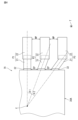
- FIG. 1 is a schematic perspective view partially showing a telescopic device according to a first embodiment of the present disclosure.
- FIG. 2 is a sectional view taken along line II-II in FIG.
- FIG. 3 is a schematic perspective view showing a telescopic device according to a second embodiment of the present disclosure.
- FIG. 4 is a schematic plan view partially showing a telescopic device according to a second embodiment of the present disclosure.
- FIG. 5 is a graph showing the relationship between stress and elongation of the expandable wiring according to the example.
- FIG. 6 is a graph showing the thickness dependence of the relationship between the expansion/contraction rate and the resistance value of the expandable wiring according to the example.
- FIG. 7 is a schematic perspective view partially showing the telescopic device according to the example.
- FIG. 8A is a diagram showing the shape of the paste applied.
- FIG. 8B is a diagram showing the shape of the paste applied.
- FIG. 1 is a schematic perspective view partially showing the telescopic device 1.
- FIG. 2 is a sectional view taken along line II-II in FIG.
- the description of the coating layer is omitted.
- the thickness direction of the stretchable base material is indicated by an arrow T.
- the "direction perpendicular to the main surface of the stretchable base material" described in the claims corresponds to the T direction.
- the direction from the main surface of the stretchable base material where the stretchable wiring is not provided to the main surface of the stretchable base material where the stretchable wire is provided is defined as the upper side.
- the stretchable device 1 includes a stretchable base material 11 having a main surface 111, an electronic component 30 provided on the main surface 111 of the stretchable base material 11, a first stretchable wiring 21 connected to the electronic component 30, and a first stretchable wire 21 connected to the electronic component 30. It includes a second elastic wiring 22 connected to the elastic wiring 21 and a covering layer 50 provided so as to cover the first elastic wiring 21 and the second elastic wiring 22.
- the stretchable device 1 is, for example, attached to a living body and used to measure biological signals.
- on the main surface of the stretchable base material does not refer to an absolute direction such as vertically upward defined in the direction of gravity, but to the outside of the stretchable base material whose boundary is the main surface of the stretchable base material. It refers to the direction toward the outside between the inside and inside. Therefore, “on the main surface of the stretchable base material” is a relative direction determined by the direction of the main surface of the stretchable base material. Furthermore, “above” an element does not only mean a position directly above the element (on), but also a position above the element that is away from the element, that is, a position above the element through another object. It also includes spaced above positions.
- the stretchable base material 11 is a sheet-like or film-like base material made of a stretchable resin material.
- the resin material include thermoplastic polyurethane (TPU).
- TPU thermoplastic polyurethane
- the thickness of the stretchable base material 11 is not particularly limited, but from the viewpoint of not inhibiting the expansion and contraction of the surface of a living body when attached to a living body, it is preferably 1 mm or less, more preferably 100 ⁇ m or less, and 50 ⁇ m or less. It is more preferable that Moreover, it is preferable that the thickness of the stretchable base material 11 is 1 ⁇ m or more.
- the shape of the stretchable base material 11 is not particularly limited. In this embodiment, the stretchable base material 10 is shaped to extend in one direction A when viewed from the thickness direction T.
- the electronic component 30 is, for example, a capacitor component, an inductor component, an IC (semiconductor integrated circuit), or the like.
- the type of electronic component 30 is not particularly limited. Although the shape of the electronic component 30 is not particularly limited, it is a rectangular parallelepiped in this embodiment.
- the electronic component 30 is arranged so that its longitudinal direction is parallel to the extending direction of the stretchable base material 11 (hereinafter referred to as the "A direction"). External electrodes 31 are provided at both ends of the electronic component 30 in the A direction, respectively.
- the first expandable wiring 21 is a member that has a function such as relieving stress applied to the expandable device 1.
- the first stretchable wiring 21 is made of a stretchable conductive material.
- metal foil such as silver, copper, or nickel may be used as the conductive material, or metal powder such as silver, copper, or nickel and elastomeric resin such as epoxy resin, urethane resin, acrylic resin, or silicone resin may be used. You may use the mixture consisting of.
- the first elastic wiring 21 has a larger Young's modulus than the second elastic wiring 22.
- the shape of the first stretchable wiring 21 is not particularly limited, in this embodiment, it has a shape extending in one direction. Specifically, the first stretchable wiring 21 is arranged so that its extending direction is parallel to the A direction.
- a first end 211 of the first expandable wiring 21 in the extending direction is connected to the electronic component 30.
- the first end 211 of the first stretchable wiring 21 in the extending direction is connected to the external electrode 31 on one side of the electronic component 30 via the connecting member 40 .
- the connecting member 40 is, for example, solder, conductive adhesive, or the like.
- the length L1 of the first stretchable wiring 21 in the extending direction is, for example, 0.2 mm or more and 5 mm or less. In this specification, the length L1 does not include the overlapping portion with the second stretchable wiring 22. It is preferable that the width W1 in the direction perpendicular to the extending direction of the first stretchable wiring 21 is, for example, 0.2 mm or more and 3.2 mm or less. It is preferable that the thickness t1 of the first stretchable wiring 21 in the T direction is, for example, 10 ⁇ m or more and 30 ⁇ m or less.
- the second telescopic wiring 22 is a wiring mainly responsible for transmitting and receiving biological signals and the like.
- the second stretchable wiring 22 is made of a stretchable conductive material.
- metal foil such as silver, copper, or nickel may be used as the conductive material, or metal powder such as silver, copper, or nickel and elastomeric resin such as epoxy resin, urethane resin, acrylic resin, or silicone resin may be used.
- elastomeric resin such as epoxy resin, urethane resin, acrylic resin, or silicone resin may be used.
- a mixture consisting of the following may also be used.
- the shape of the second stretchable wiring 22 is not particularly limited, in this embodiment, it has a shape extending in one direction. Specifically, the second stretchable wiring 22 is arranged so that its extending direction is parallel to the A direction.
- the extending direction of the second stretchable wiring 22 is parallel to the extending direction of the first stretchable wiring 21.
- Parallel in this application is not limited to a strict parallel relationship, but also includes a substantial parallel relationship, taking into consideration the range of realistic variations.
- a first end 221 of the second stretchable wiring 22 in the extending direction is connected to a second end 212 of the first stretchable wiring 21 in the extending direction.
- the first end 221 of the second stretchable wiring 22 in the extending direction is stacked on the second end 212 of the first stretchable wiring 21 in the extending direction. It is connected to the second end 212 in the extending direction.
- the present invention is not limited to this, and the second end 212 of the first stretchable wiring 21 in the extending direction is stacked on the first end 221 of the second stretchable wiring 22 in the extending direction, so that the second stretchable wiring 21 may be connected to the first end 221 in the extending direction.
- the length L3 in the A direction of a portion (overlapping portion) 22P of the second stretchable wiring 22 that overlaps with the first stretchable wire 21 is, for example, 0.1 mm or more and 1 mm or less.
- the length L2 of the second stretchable wiring 22 in the extending direction is, for example, three times or more the length L1. In this specification, the length L2 does not include the overlapping portion with the first expandable wiring 21. Further, as shown in FIG. 7, which will be described later, when there are a plurality of electronic components 30 and one second telescoping wiring 22 is connected to the plurality of electronic components 30, L2 is the extension of the second telescoping wiring 22. The length is defined as the midpoint between the electronic components 30 adjacent to each other in the direction. It is preferable that the width W2 of the second stretchable wiring 22 in the direction perpendicular to the extending direction is, for example, 0.2 mm or more and 3.2 mm or less. It is preferable that the thickness t2 of the second stretchable wiring 22 in the T direction is, for example, 10 ⁇ m or more and 30 ⁇ m or less.
- the set of stretchable wiring includes the first stretchable wire 21 connected to the external electrode 31 of the electronic component 30 and the second stretchable wire 22 connected to the first stretchable wire 21.
- the covering layer 50 protects the first elastic wiring 21 and the second elastic wiring 22 from the external environment.
- the covering layer 50 is, for example, potting resin.
- the coating layer 50 is preferably made of a stretchable resin material, such as an ionomer resin, a polyester resin, a styrene resin, an olefin resin, an epoxy resin, a urethane resin, an acrylic resin, or a silicone resin. It is more preferable that Although the covering layer 50 does not need to be provided, it is preferable to cover at least the connecting portion between the first expandable wiring 21 and the electronic component 30.
- the first end 211 of the first elastic wiring 21 in the extending direction is connected to the electronic component 30, and the second end 212 of the first elastic wiring 21 in the extending direction is connected to the second end 211 of the first elastic wiring 21 in the extending direction. Since it is connected to the first end 221 of the stretchable wiring 22 in the extending direction, the end of the electronic component 30 is connected to the first stretchable wiring 21 and the first end when viewed from the direction perpendicular to the main surface 111 of the stretchable base 11. 2 does not overlap with the connection part with the expandable wiring 22.
- the connecting member 40 that connects the electronic component 30 and the first telescopic wiring 21 can also be arranged so as not to overlap the connecting portion between the first telescopic wiring 21 and the second telescopic wiring 22.
- different members can be arranged stepwise from the end of the electronic component 30 toward the second expandable wiring 22.
- the stress that may be concentrated at the connection portion between the electronic component 30 and the first elastic wiring 21 can be dispersed from the end of the electronic component 30 toward the second elastic wiring 22, and the concentration of stress can be alleviated.
- the mechanical strength of the stretchable device 1 can be improved.
- the telescopic device 1 satisfies the following formulas (1) and (2).
- ⁇ Total displacement of the first elastic wiring 21 and the second elastic wiring 22
- L2 Length of the second elastic wiring 22 in the elastic direction
- S1 Cross-sectional area of the first elastic wiring 21 in a cross section perpendicular to the expansion/contraction direction (width W1
- the above ⁇ 1 means the tensile load that acts on the first elastic wiring 21 when the displacement amount ⁇ is applied to the entire first elastic wiring 21 and the second elastic wiring 22.
- the above ⁇ 2 means the tensile load that acts on the second elastic wiring 22 when the displacement amount ⁇ is applied to the entire first elastic wiring 21 and the second elastic wiring 22. That is, satisfying the above formula (1) and formula (2) means that each of the first tensile load ratio and the second tensile load ratio calculated by the following formula is 1 or less.
- First tensile load ratio (Tensile load ⁇ 1 acting on the first elastic wiring 21) / (Allowable stress ⁇ 1 max of the first elastic wiring 21)
- Second tensile load ratio (Tensile load ⁇ 2 acting on the second elastic wiring 22) / (Allowable stress ⁇ 2 max of the second elastic wiring 22)
- the tensile load ⁇ 1 and the tensile load ⁇ 2 are derived by the following formula using the above load F.
- the elastic modulus E1, E2, the lengths L1, L2 in the elastic direction, the cross-sectional areas S1, S2, and the The tensile load ⁇ 1 and the tensile load ⁇ 2 can be adjusted by adjusting the length L3 of the portion where the first elastic wiring 21 and the second elastic wiring 22 overlap each other. Note that when the length of each member of the first elastic wiring 21 and the second elastic wiring 22 in the extending direction is a predetermined length, the portion where the first elastic wiring 21 and the second elastic wiring 22 overlap each other By adjusting the length of , it is possible to adjust the lengths L1 and L2 of the first stretchable wiring 21 and the second stretchable wiring 22 in the stretching direction.
- the allowable stress ⁇ 1 max of the first elastic wiring 21 in the above formula (1) is the stress at the maximum elongation of the first elastic wiring 21.
- the allowable stress ⁇ 1 max of the first elastic wiring 21 can be determined by, for example, the relationship between elongation and stress of the first elastic wiring 21 (stress-strain diagram) after cutting the first elastic wiring 21 to a predetermined length in the extending direction. may be measured to determine the stress at which the first expandable wiring 21 breaks.
- the allowable stress ⁇ 2 max of the second stretchable wiring 22 in the above formula (2) is the stress at the maximum elongation of the second stretchable wiring 22.
- the allowable stress ⁇ 2 max of the second elastic wiring 22 can be determined by, for example, cutting out the second elastic wiring 22 to a predetermined length in the extending direction, and then measuring the relationship between the elongation and stress of the second elastic wiring 22. This may be the stress when the wiring 22 breaks.
- the first tensile load ratio being 1 or less means that the tensile load ⁇ 1 acting on the first elastic wiring 21 is smaller than the allowable stress ⁇ 1 max of the first elastic wiring 21. That is, it means that the selected configuration of the first stretchable wiring 21 means that the first stretchable wiring 21 does not break and the mechanical strength of the first stretchable wiring 21 is sufficient.
- the second tensile load ratio being 1 or less means that the tensile load ⁇ 2 acting on the second elastic wiring 22 is smaller than the allowable stress ⁇ 2 max of the second elastic wiring 22. That is, if the configuration of the second stretchable wiring 22 is selected, it means that the second stretchable wiring 22 does not break and the mechanical strength of the second stretchable wiring 22 is sufficient.
- each of the first tensile load ratio and the second tensile load ratio is 1 or less, so each of the first elastic wiring 21 and the second elastic wiring 22 is broken. It is possible to prevent this from happening. Further, by satisfying the above formulas (1) and (2), the shape and material of the first telescopic wiring 21 and the second telescopic wiring 22 can be determined in accordance with the displacement amount ⁇ . Therefore, the displacement amount ⁇ falls within a range in which the telescopic device 1 does not break.
- connection member 40 further includes a connecting member 40 that connects the electronic component 30 and the first stretchable wiring 21, and when viewed from the direction (T direction) perpendicular to the main surface 111 of the stretchable base material 11, the connecting member 40 is connected to the second stretchable wire 21. It does not overlap with the first end 221 of the wiring 22 in the extending direction. According to this configuration, when the connection member 40 is made of solder, for example, it is possible to suppress the thermal influence on the second expandable wiring 22 during the formation of the connection member 40 .
- the solder erosion resistance of the first elastic wiring 21 is higher than the solder erosion resistance of the second elastic wiring 22.
- Solder erosion is a phenomenon in which metal, etc. in the stretchable wiring melts into the solder, reducing the volume of the stretchable wiring. According to this configuration, when the connection member 40 is solder, the connection reliability between the first expandable wiring 21 and the connection member 40 can be improved.
- a stretchable wire is immersed in molten solder, and a graph showing the relationship between the immersion time and the amount of metal in the melted stretchable wire is created. It can be evaluated that the larger the slope of the graph, the more likely it is to be eaten by solder, that is, the resistance to solder eating is low.
- the solubility (chemical attack) of the first stretchable wiring 21 in the resin is smaller than the solubility (chemical attack) of the second stretchable wiring 22 in the resin.
- the covering layer 50 is made of, for example, a potting resin and covers at least the connecting portion between the electronic component 30 and the first elastic wiring 21, the material of the first elastic wiring 21 is not applied to the coating layer 50. Dissolution can be suppressed.
- the solubility of the stretchable wiring in resin can be evaluated based on, for example, JIS K 7114:2001 (ISO 175:1999).
- This test method involves completely immersing the specimen in a test liquid at a specified temperature and for a specified time. The mass of the test piece is measured before immersion, and after removal from the test solution and, if necessary, after drying. It can be evaluated that the greater the mass change, the greater the solubility in the test liquid (the greater the chemical attack).
- the length L1 of the first stretchable wiring 21 in the extending direction is shorter than the length L2 of the second stretchable wiring 22 in the extending direction. According to this configuration, even if the first elastic wiring 21 is harder than the second elastic wiring 22, the influence on the elasticity of the elastic device 1 can be suppressed.
- the Young's modulus (elastic modulus) of the first elastic wiring 21 is larger than the Young's modulus (elastic modulus) of the second elastic wiring 22.
- the first stretchable wiring 21 can be made harder than the second stretchable wiring 22. Therefore, the hardness can be gradually softened from the end of the electronic component 30 toward the second expandable wiring 22. As a result, stress that may be concentrated at the connection portion between the electronic component 30 and the first expandable wiring 21 can be further alleviated.
- the thickness t1 of the first elastic wiring 21 is larger than the thickness t2 of the second elastic wiring 22. According to this configuration, the solder bite resistance of the first expandable wiring 21 can be further improved. Furthermore, since the allowable stress ⁇ 1 max of the first expandable wiring 21 can be increased, the first tensile load ratio can be further reduced. Furthermore, since the clearance between the electronic component 30 and the stretchable base material 11 can be increased, the ability to fill the clearance with the coating layer 50 can be improved.
- the viscosity of the material for the first elastic wiring 21 is greater than the viscosity of the material for the second elastic wiring 22.
- the thickness t1 of the first stretchable wiring 21 can be made larger than the thickness t2 of the second stretchable wiring 22 more reliably.
- the first stretchable wire 21 is made of a thermosetting material
- the second stretchable wire 22 is made of a thermoplastic material
- the first end 221 of the second stretchable wire 22 in the extending direction is made of the first stretchable wire 22. It is laminated on the second end portion 212 of the wiring 21 in the extending direction. According to this configuration, even when stress is applied to the stretchable device 1, interface peeling between the first stretchable wiring 21 and the second stretchable wire 22 is suppressed, and the mechanical strength of the stretchable device 1 is further improved. Can be done.
- FIG. 3 is a schematic perspective view of the telescopic device 1A.
- FIG. 4 is a schematic plan view partially showing the telescopic device 1A. Specifically, FIG. 4 is a diagram of the lower right portion of the page of FIG. 3 viewed from above.
- the elastic device 1A is different from the elastic device 1 according to the first embodiment in the configurations of electronic components, first elastic wiring, and second elastic wiring.
- the electronic component 30A has a regular square prism shape.
- a plurality of external electrodes 32 are provided on the outer periphery of the lower surface of the electronic component 30A.
- the first elastic wiring 21 and the second elastic wiring 22 each exist in plural numbers, and include a first elastic wiring 21 connected to the electronic component 30A and a second elastic wiring 22 connected to the first elastic wiring 21. There are a plurality of sets of expandable wiring. Specifically, one first elastic wiring 21 is connected to one external electrode 32 of the electronic component 30A, and one second elastic wiring 22 is connected to one first elastic wiring 21. ing. A plurality of sets of stretchable wires each including the one first stretchable wire 21 and the one second stretchable wire 22 exist corresponding to each external electrode 32 .
- each first stretchable wire 21 in the plurality of sets of stretchable wires is radial with respect to the center C of the electronic component 30A.
- the extending direction of the first telescopic wiring 21 in one set of telescopic wiring is different from that in the other set.
- the angle formed by the extending direction of the first stretchable wiring 21 in the set of stretchable wiring is greater than 0° and less than or equal to 90°.
- each first telescopic wiring 21 in the first telescopic wiring group P1, the second telescopic wiring group P2, and the third telescopic wiring group P3 is located at the center of the electronic component 30A. They are arranged on the outer periphery of the electronic component 30A so as to be radial with respect to C.
- the extending direction of the first telescopic wiring 21 in the first telescopic wiring set P1 and the second telescopic wiring set P2 adjacent to each other along the outer periphery of the electronic component 30A the extending direction of the first telescopic wiring 21 in the first telescopic wiring set P1 and the second telescopic wiring
- the angle ⁇ 1 formed by the extending direction of the first elastic wiring 21 in the group P2 is greater than 0° and less than or equal to 90°.
- the extending direction of the first telescoping wiring 21 in the second telescoping wiring set P2 and the third telescoping wiring set P3 adjacent to each other along the outer periphery of the electronic component 30A the extending direction of the first telescoping wiring 21 in the second telescoping wiring set P2 and the third telescoping wiring
- the angle ⁇ 2 formed by the extending direction of the first telescopic wiring 21 in the group P3 is greater than 0° and less than or equal to 90°.
- each second telescoping wiring 22 is The directions are parallel to each other, but they may be arranged at an angle to each other.
- each first telescoping wiring 21 in the plurality of telescoping wiring sets is arranged on the outer periphery of the electronic component 30A so as to be radial with respect to the center C of the electronic component 30A.
- the inter-electrode pitch WP can be made different from the inter-electrode pitch EP.
- the periphery of the electronic component 30A can be covered with the first stretchable wiring 21 which is softer than the electronic component 30A. Therefore, even if tensile stress is applied to the stretchable device 1A, stress that may be concentrated at the connection portion between the electronic component 30A and the first stretchable wiring 21 can be further alleviated. Further, even when tensile stress is applied to the elastic device 1A from any direction, shear deformation at the most affected portion can be reduced, and the durability of the elastic device 1A can be improved.
- each embodiment is an example, and the present disclosure is not limited to each embodiment.
- each drawing is an illustration of the constituent elements, and does not limit the shape.
- partial substitution or combination of the configurations shown in different embodiments is possible.
- Example 1 The elongation against stress was measured for the first stretchable wiring and the second stretchable wiring.
- FIG. 5 is a graph showing the relationship between stress and elongation of the first stretchable wiring and the second stretchable wiring.
- Graph G1 is the result for the first telescopic wiring.
- Graph G2 is the result for the second telescopic wiring.
- the first stretchable wiring broke at about 7% elongation.
- the stress at this time was about 16 MPa. That is, the allowable stress of the first expandable wiring was about 16 MPa.
- the second stretchable wiring broke at about 17% elongation.
- the stress at this time was about 3 MPa. That is, the allowable stress of the second expandable wiring was about 3 MPa.
- FIG. 6 is a graph showing the thickness dependence of the relationship between the expansion/contraction rate and the resistance value of the first expansion/contraction wiring.
- Example 2 The range of tensile load F that can be used without breaking the elastic device was calculated. The calculation below is an example, and the range of tensile load F that can be used without breaking the elastic device depends on the material and shape of the elastic base material, the material and shape of the first and second elastic wiring, and the number of electronic components. and may vary depending on location, etc.
- the tensile load F that can be used without breaking the expansion/contraction device 1 is calculated by the following formula.
- the expansion/contraction ratio ⁇ can be defined, for example, as the ratio of the above-mentioned displacement amount ⁇ to the length of the entire expansion/contraction base material before expansion/contraction.
- Tensile load F E ⁇ ( ⁇ /100) ⁇ S that can be used without breaking the elastic device 1 however, E: Composite elastic modulus (composite elastic modulus) of the elastic base material 11, the first elastic wiring 21, and the second elastic wiring 22 S: Cross-sectional area of the stretchable base material 11 in a cross section perpendicular to the stretch direction
- FIG. 7 is a schematic perspective view partially showing the telescopic device 1B according to the second embodiment.
- a wiring/component group in which the second stretchable wiring 22, the first stretchable wire 21, the electronic component 30, and the first stretchable wire 21 are connected in this order is arranged along the A direction. Connected repeatedly. A plurality of these repeatedly connected wiring/component groups exist in a direction perpendicular to the A direction. In FIG. 7, the directions of expansion and contraction are indicated by arrows.
- the broken line in the area AR in FIG. 7 indicates an imaginary line connecting the midpoints between adjacent electronic components 30. Note that although the area AR is depicted as being square in FIG. 7, the area AR is not necessarily square.
- the center of gravity of the region AR overlaps with the electronic component 30 when viewed from the T direction.
- the area of the region AR is the value obtained by dividing the area of the entire base material by the number of electronic components 30.
- the area of the region AR was 10 mm 2 and the expansion/contraction ratio ⁇ EX was 20%.
- Table 1 shows the elastic modulus (elastic modulus, Young's modulus), cross-sectional area in a cross section perpendicular to the stretching direction, length in the stretching direction, and composite elastic modulus of the stretchable base material, the first stretchable wiring, and the second stretchable wire in the area AR. It was shown to.
- the composite elastic modulus was roughly estimated from the elastic modulus, cross-sectional area, and length of each member.
- the elastic base material was assumed to be thermoplastic polyurethane (TPU).
- TPU thermoplastic polyurethane
- the length of the second stretchable wiring 22 in the stretch direction is the sum of the length L2a and the length L2b.
- the length of the stretchable base material in the stretch direction is the total value of length L1a, length L1b, length L2a, and length L2b.
- Example 3 A paste was used as the material for the first elastic wiring, and the relationship between the viscosity of the paste and the thickness of the first elastic wiring to be formed was investigated. Since the first stretchable wiring has an island shape, it can be printed using a metal mask, and it is possible to use a paste that has increased thixotropy, that is, the viscosity of the paste, by adding a thixotropic agent. The paste was printed using a metal mask to form the first stretchable wiring.
- FIG. 8A is a diagram showing the applied shape of paste M1 to which no thixotropic agent is added.
- FIG. 8B is a diagram showing the application shape of paste M2 containing a thixotropic agent.
- the paste spread and had a thickness of about 25 ⁇ m.
- the paste did not spread and the thickness was about 50 ⁇ m. It was found that the thickness of the first stretchable wiring could be made thicker with paste M2 whose viscosity was increased by adding a thixotropic agent.
- a sample in which the first elastic wiring had a thickness of 10 ⁇ m and a sample in which the first elastic wiring had a thickness of 50 ⁇ m were prepared. Then, for each sample, the solder thickness and the number of reflows were varied, and the resistance to solder eating was evaluated. The thickness of the solder was changed to 20 ⁇ m, 50 ⁇ m, 80 ⁇ m, 110 ⁇ m, and 140 ⁇ m. The number of reflows was changed to 1, 2, 3, 4, and 5 times. Solder eating was observed in the sample in which the first elastic wiring had a thickness of 10 ⁇ m, but no solder eating was observed in the sample in which the first elastic wiring had a thickness of 50 ⁇ m. It has been found that by increasing the thickness of the first stretchable wiring, the resistance to solder eating is improved.
- Example 4 The relationship between the stacking order of the first stretchable wiring and the second stretchable wiring and interfacial peeling was investigated. Specifically, the first end of the second stretchable wiring is laminated on the second end of the first stretchable wiring as shown in FIG. 2, and the second end of the first stretchable wiring It was investigated whether the behavior in which interfacial peeling occurs is different depending on the case where the first end of the second stretchable wiring is laminated on the first end of the second stretchable wiring. A thermosetting material was used as the material for the first stretchable wiring. A thermoplastic material was used as the material for the second stretchable wiring. Table 2 shows the results when the first end of the second stretchable wiring was laminated on the second end of the first stretchable wiring.
- Table 3 shows the results when the second end of the first stretchable wiring was laminated on the first end of the second stretchable wiring.
- the numerical value described as "0.16 N/mm" means the tensile load per unit width at the time of interfacial peeling.
- Cohesive failure is a condition in which the interface between the first and second stretchable wirings does not separate, but the breakage occurs inside either the first or second stretchable wires. It is.
- thermosetting material is used as the material of the first elastic wiring and a thermoplastic material is used as the material of the second elastic wiring
- the first end of the second elastic wiring is placed above the second end of the first elastic wiring. It was found that interfacial delamination is suppressed and mechanical strength is improved when laminated on the substrate.
- the present disclosure includes the following aspects. ⁇ 1> a stretchable base material having a main surface; an electronic component provided on the main surface of the stretchable base material; a first telescopic wiring connected to the electronic component; a second stretchable wiring connected to the first stretchable wiring, A first end in the extending direction of the first stretchable wiring is connected to the electronic component, A stretchable device, wherein a second end of the first stretchable wiring in the extending direction is connected to a first end of the second stretchable wiring in the extending direction.
- the telescopic device according to ⁇ 1> which satisfies the following formula.
- ⁇ 1 ⁇ 0.80 ⁇ allowable stress of first stretchable wiring ⁇ 2 ⁇ 0.80 ⁇ allowable stress of second stretchable wire ⁇ 4> The telescopic device according to ⁇ 2>, which further satisfies the following formula. ⁇ 1 ⁇ 0.50 ⁇ allowable stress of first stretchable wiring ⁇ 2 ⁇ 0.50 ⁇ allowable stress of second stretchable wire ⁇ 5> further comprising a connecting member connecting the electronic component and the first stretchable wiring, Any one of ⁇ 1> to ⁇ 4>, wherein the connection member does not overlap the first end in the extending direction of the second stretchable wiring when viewed from a direction perpendicular to the main surface of the stretchable base material.
- each of the first stretchable wiring and the second stretchable wiring There are a plurality of each of the first stretchable wiring and the second stretchable wiring, There are a plurality of sets of stretchable wiring, each consisting of the first stretchable wire connected to the electronic component and the second stretchable wire connected to the first stretchable wire, from ⁇ 1> to ⁇ 5.
- each first stretchable wire in the plurality of sets of stretchable wires extends around the outer periphery of the electronic component so as to be radial with respect to the center of the electronic component.
- the extending direction of the first stretchable wiring in one set of stretchable wires and the first stretchable wire in the other set of stretchable wires are The telescopic device according to ⁇ 6>, wherein the angle formed by the extending direction of the wiring is greater than 0° and less than or equal to 90°.
- ⁇ 10> The stretchable device according to any one of ⁇ 1> to ⁇ 9>, wherein the length of the first stretchable wiring in the extending direction is shorter than the length of the second stretchable wiring in the extending direction.
- ⁇ 11> The elastic device according to any one of ⁇ 1> to ⁇ 10>, wherein a Young's modulus of the first elastic wiring is larger than a Young's modulus of the second elastic wiring.
- ⁇ 12> The elastic device according to any one of ⁇ 1> to ⁇ 11>, wherein the first elastic wiring has a thickness greater than the second elastic wiring.
- the elastic device according to any one of ⁇ 1> to ⁇ 12>, wherein the viscosity of the material of the first elastic wiring is greater than the viscosity of the material of the second elastic wiring.
- the first stretchable wiring is made of a thermosetting material
- the second stretchable wiring is made of a thermoplastic material
- the first end in the extending direction of the second stretchable wiring is one of ⁇ 1> to ⁇ 13>, which is laminated on the second end in the extending direction of the first stretchable wiring.
- Telescoping device as described.
- Elastic device 11 Elastic base material 111: Main surface 21: First elastic wiring 211: First end of first elastic wiring 212: Second end of first elastic wiring 22: Second elastic Wiring 221: First end of second elastic wiring 222: Second end of second elastic wiring 30, 30A: Electronic components 31, 32: External electrode 40: Connection member 50: Covering layer C: Center L1: Length of the first elastic wiring L2: Length of the second elastic wiring P1, P2, P3: Set of elastic wiring t1: Thickness of the first elastic wiring t2: Thickness of the second elastic wiring W1: Thickness of the second elastic wiring Width of 1st stretch wiring W2: Width of 2nd stretchable wire
Landscapes
- Engineering & Computer Science (AREA)
- Microelectronics & Electronic Packaging (AREA)
- Structure Of Printed Boards (AREA)
Priority Applications (3)
| Application Number | Priority Date | Filing Date | Title |
|---|---|---|---|
| CN202380050370.3A CN119452737A (zh) | 2022-06-30 | 2023-06-21 | 伸缩器件 |
| JP2024530735A JP7643644B2 (ja) | 2022-06-30 | 2023-06-21 | 伸縮デバイス |
| US18/983,657 US20250120012A1 (en) | 2022-06-30 | 2024-12-17 | Stretchable device |
Applications Claiming Priority (2)
| Application Number | Priority Date | Filing Date | Title |
|---|---|---|---|
| JP2022106362 | 2022-06-30 | ||
| JP2022-106362 | 2022-06-30 |
Related Child Applications (1)
| Application Number | Title | Priority Date | Filing Date |
|---|---|---|---|
| US18/983,657 Continuation US20250120012A1 (en) | 2022-06-30 | 2024-12-17 | Stretchable device |
Publications (1)
| Publication Number | Publication Date |
|---|---|
| WO2024004783A1 true WO2024004783A1 (ja) | 2024-01-04 |
Family
ID=89382262
Family Applications (1)
| Application Number | Title | Priority Date | Filing Date |
|---|---|---|---|
| PCT/JP2023/022959 Ceased WO2024004783A1 (ja) | 2022-06-30 | 2023-06-21 | 伸縮デバイス |
Country Status (4)
| Country | Link |
|---|---|
| US (1) | US20250120012A1 (https=) |
| JP (1) | JP7643644B2 (https=) |
| CN (1) | CN119452737A (https=) |
| WO (1) | WO2024004783A1 (https=) |
Cited By (2)
| Publication number | Priority date | Publication date | Assignee | Title |
|---|---|---|---|---|
| WO2025173538A1 (ja) * | 2024-02-13 | 2025-08-21 | 株式会社村田製作所 | 伸縮性デバイス |
| WO2025249078A1 (ja) * | 2024-05-27 | 2025-12-04 | 株式会社村田製作所 | 伸縮性デバイス |
Citations (4)
| Publication number | Priority date | Publication date | Assignee | Title |
|---|---|---|---|---|
| WO2017065270A1 (ja) * | 2015-10-16 | 2017-04-20 | 国立研究開発法人科学技術振興機構 | 応力緩和基板及びテキスタイル型デバイス |
| JP2017143257A (ja) * | 2016-02-05 | 2017-08-17 | 日本メクトロン株式会社 | 伸縮基板モジュール、伸縮性配線基板及びそれらの製造方法 |
| JP2018186214A (ja) * | 2017-04-27 | 2018-11-22 | セイコーエプソン株式会社 | 伸縮性回路基板およびひずみセンサー |
| JP2019029514A (ja) * | 2017-07-31 | 2019-02-21 | セイコーエプソン株式会社 | 配線デバイスおよびひずみセンサー |
Family Cites Families (2)
| Publication number | Priority date | Publication date | Assignee | Title |
|---|---|---|---|---|
| JP5220766B2 (ja) * | 2007-12-26 | 2013-06-26 | 株式会社フジクラ | 実装基板 |
| CN114846911B (zh) * | 2020-09-29 | 2025-06-03 | 株式会社村田制作所 | 伸缩性安装基板以及伸缩性安装基板的制造方法 |
-
2023
- 2023-06-21 CN CN202380050370.3A patent/CN119452737A/zh active Pending
- 2023-06-21 WO PCT/JP2023/022959 patent/WO2024004783A1/ja not_active Ceased
- 2023-06-21 JP JP2024530735A patent/JP7643644B2/ja active Active
-
2024
- 2024-12-17 US US18/983,657 patent/US20250120012A1/en active Pending
Patent Citations (4)
| Publication number | Priority date | Publication date | Assignee | Title |
|---|---|---|---|---|
| WO2017065270A1 (ja) * | 2015-10-16 | 2017-04-20 | 国立研究開発法人科学技術振興機構 | 応力緩和基板及びテキスタイル型デバイス |
| JP2017143257A (ja) * | 2016-02-05 | 2017-08-17 | 日本メクトロン株式会社 | 伸縮基板モジュール、伸縮性配線基板及びそれらの製造方法 |
| JP2018186214A (ja) * | 2017-04-27 | 2018-11-22 | セイコーエプソン株式会社 | 伸縮性回路基板およびひずみセンサー |
| JP2019029514A (ja) * | 2017-07-31 | 2019-02-21 | セイコーエプソン株式会社 | 配線デバイスおよびひずみセンサー |
Cited By (2)
| Publication number | Priority date | Publication date | Assignee | Title |
|---|---|---|---|---|
| WO2025173538A1 (ja) * | 2024-02-13 | 2025-08-21 | 株式会社村田製作所 | 伸縮性デバイス |
| WO2025249078A1 (ja) * | 2024-05-27 | 2025-12-04 | 株式会社村田製作所 | 伸縮性デバイス |
Also Published As
| Publication number | Publication date |
|---|---|
| JP7643644B2 (ja) | 2025-03-11 |
| US20250120012A1 (en) | 2025-04-10 |
| JPWO2024004783A1 (https=) | 2024-01-04 |
| CN119452737A (zh) | 2025-02-14 |
Similar Documents
| Publication | Publication Date | Title |
|---|---|---|
| WO2024004783A1 (ja) | 伸縮デバイス | |
| EP3255964A1 (en) | Stretchable circuit board | |
| US5969424A (en) | Semiconductor device with pad structure | |
| CN104716104B (zh) | 半导体装置以及半导体装置的制造方法 | |
| US10163844B2 (en) | Semiconductor device having conductive bumps of varying heights | |
| JP3178881U (ja) | 集積回路素子パッケージ構造 | |
| KR20010031110A (ko) | 마이크로전자 패키지를 열적으로 향상시키는 방법 및 구조체 | |
| EP2863419B1 (en) | Semiconductor device | |
| CN112635410A (zh) | 功率模块 | |
| US20160190058A1 (en) | Semiconductor Device | |
| US20150115442A1 (en) | Redistribution layer and method of forming a redistribution layer | |
| TW201939708A (zh) | 半導體裝置 | |
| JP2009224617A (ja) | 配線基板 | |
| EP1494280B1 (en) | System and method for increasing the strength of a bond made by a small diameter wire in a ball bonding | |
| JP4045261B2 (ja) | 半導体装置 | |
| US12424383B2 (en) | Semiconductor device | |
| JP7540610B2 (ja) | モジュール及び半導体複合装置 | |
| WO2023171464A1 (ja) | 伸縮性デバイス | |
| JP4010298B2 (ja) | 半導体装置及びその製造方法、回路基板並びに電子機器 | |
| JP7443875B2 (ja) | 伸縮性電子部品及び伸縮性電子部品実装基板 | |
| WO2023105873A1 (ja) | 伸縮デバイス | |
| EP3279909A1 (en) | Capacitor and method for manufacturing same | |
| US20150022987A1 (en) | Electronic device comprising an integrated circuit chip provided with projecting electrical connection pads | |
| JP7605343B2 (ja) | 伸縮デバイス | |
| JP4701779B2 (ja) | 集積回路パッケージ組立構造 |
Legal Events
| Date | Code | Title | Description |
|---|---|---|---|
| 121 | Ep: the epo has been informed by wipo that ep was designated in this application |
Ref document number: 23831229 Country of ref document: EP Kind code of ref document: A1 |
|
| WWE | Wipo information: entry into national phase |
Ref document number: 2024530735 Country of ref document: JP |
|
| WWE | Wipo information: entry into national phase |
Ref document number: 202380050370.3 Country of ref document: CN |
|
| NENP | Non-entry into the national phase |
Ref country code: DE |
|
| WWP | Wipo information: published in national office |
Ref document number: 202380050370.3 Country of ref document: CN |
|
| 122 | Ep: pct application non-entry in european phase |
Ref document number: 23831229 Country of ref document: EP Kind code of ref document: A1 |