WO2024004783A1 - 伸縮デバイス - Google Patents
伸縮デバイス Download PDFInfo
- Publication number
- WO2024004783A1 WO2024004783A1 PCT/JP2023/022959 JP2023022959W WO2024004783A1 WO 2024004783 A1 WO2024004783 A1 WO 2024004783A1 JP 2023022959 W JP2023022959 W JP 2023022959W WO 2024004783 A1 WO2024004783 A1 WO 2024004783A1
- Authority
- WO
- WIPO (PCT)
- Prior art keywords
- wiring
- stretchable
- elastic
- electronic component
- extending direction
- Prior art date
Links
- 239000000463 material Substances 0.000 claims abstract description 74
- 229910000679 solder Inorganic materials 0.000 claims description 23
- 230000008602 contraction Effects 0.000 claims description 18
- 229920005989 resin Polymers 0.000 claims description 16
- 239000011347 resin Substances 0.000 claims description 16
- 238000006073 displacement reaction Methods 0.000 claims description 9
- 239000012815 thermoplastic material Substances 0.000 claims description 6
- 229920001187 thermosetting polymer Polymers 0.000 claims description 6
- 239000004020 conductor Substances 0.000 description 10
- PXHVJJICTQNCMI-UHFFFAOYSA-N Nickel Chemical compound [Ni] PXHVJJICTQNCMI-UHFFFAOYSA-N 0.000 description 8
- 239000002184 metal Substances 0.000 description 8
- 229910052751 metal Inorganic materials 0.000 description 8
- 229920002803 thermoplastic polyurethane Polymers 0.000 description 7
- 238000010586 diagram Methods 0.000 description 6
- 239000010410 layer Substances 0.000 description 6
- 239000013008 thixotropic agent Substances 0.000 description 6
- 239000002131 composite material Substances 0.000 description 5
- RYGMFSIKBFXOCR-UHFFFAOYSA-N Copper Chemical compound [Cu] RYGMFSIKBFXOCR-UHFFFAOYSA-N 0.000 description 4
- BQCADISMDOOEFD-UHFFFAOYSA-N Silver Chemical compound [Ag] BQCADISMDOOEFD-UHFFFAOYSA-N 0.000 description 4
- 239000004433 Thermoplastic polyurethane Substances 0.000 description 4
- 239000011247 coating layer Substances 0.000 description 4
- 229910052802 copper Inorganic materials 0.000 description 4
- 239000010949 copper Substances 0.000 description 4
- 229910052759 nickel Inorganic materials 0.000 description 4
- 229910052709 silver Inorganic materials 0.000 description 4
- 239000004332 silver Substances 0.000 description 4
- 229920000178 Acrylic resin Polymers 0.000 description 3
- 239000004925 Acrylic resin Substances 0.000 description 3
- 238000004364 calculation method Methods 0.000 description 3
- 239000003822 epoxy resin Substances 0.000 description 3
- 230000003628 erosive effect Effects 0.000 description 3
- 229920000647 polyepoxide Polymers 0.000 description 3
- 229920002050 silicone resin Polymers 0.000 description 3
- 239000000126 substance Substances 0.000 description 3
- PPBRXRYQALVLMV-UHFFFAOYSA-N Styrene Chemical compound C=CC1=CC=CC=C1 PPBRXRYQALVLMV-UHFFFAOYSA-N 0.000 description 2
- 230000007423 decrease Effects 0.000 description 2
- 239000011888 foil Substances 0.000 description 2
- 230000005484 gravity Effects 0.000 description 2
- 238000007654 immersion Methods 0.000 description 2
- 239000007788 liquid Substances 0.000 description 2
- 239000000203 mixture Substances 0.000 description 2
- 238000004382 potting Methods 0.000 description 2
- 239000000843 powder Substances 0.000 description 2
- 230000002829 reductive effect Effects 0.000 description 2
- 239000000853 adhesive Substances 0.000 description 1
- 230000001070 adhesive effect Effects 0.000 description 1
- 230000015572 biosynthetic process Effects 0.000 description 1
- 239000003990 capacitor Substances 0.000 description 1
- 239000000470 constituent Substances 0.000 description 1
- 230000032798 delamination Effects 0.000 description 1
- 238000009795 derivation Methods 0.000 description 1
- 238000004090 dissolution Methods 0.000 description 1
- 238000001035 drying Methods 0.000 description 1
- 230000000694 effects Effects 0.000 description 1
- 230000002401 inhibitory effect Effects 0.000 description 1
- 229920000554 ionomer Polymers 0.000 description 1
- 239000000155 melt Substances 0.000 description 1
- 238000000034 method Methods 0.000 description 1
- 230000036961 partial effect Effects 0.000 description 1
- 229920001225 polyester resin Polymers 0.000 description 1
- 239000004645 polyester resin Substances 0.000 description 1
- 229920005672 polyolefin resin Polymers 0.000 description 1
- 239000004065 semiconductor Substances 0.000 description 1
- 238000006467 substitution reaction Methods 0.000 description 1
- 239000000758 substrate Substances 0.000 description 1
- 238000010998 test method Methods 0.000 description 1
- 239000012085 test solution Substances 0.000 description 1
Images


Classifications
-
- H—ELECTRICITY
- H05—ELECTRIC TECHNIQUES NOT OTHERWISE PROVIDED FOR
- H05K—PRINTED CIRCUITS; CASINGS OR CONSTRUCTIONAL DETAILS OF ELECTRIC APPARATUS; MANUFACTURE OF ASSEMBLAGES OF ELECTRICAL COMPONENTS
- H05K1/00—Printed circuits
- H05K1/02—Details
-
- H—ELECTRICITY
- H05—ELECTRIC TECHNIQUES NOT OTHERWISE PROVIDED FOR
- H05K—PRINTED CIRCUITS; CASINGS OR CONSTRUCTIONAL DETAILS OF ELECTRIC APPARATUS; MANUFACTURE OF ASSEMBLAGES OF ELECTRICAL COMPONENTS
- H05K1/00—Printed circuits
- H05K1/02—Details
- H05K1/09—Use of materials for the conductive, e.g. metallic pattern
Definitions
- the present disclosure relates to a telescopic device.
- This expansion/contraction device includes an insulating base material, a first conductor having a land provided on the insulating base material, a second conductor provided on the land, and a first conductor provided separately on the second conductor. and an electronic component having electrode portions each independently contacting the solder.
- the ends of the electronic components are placed overlapping regions of the first and second conductors.
- the solder provided on the second conductor is also placed overlapping the overlapping area.
- an object of the present disclosure is to provide a stretchable device that can improve mechanical strength.
- a telescoping device includes: a stretchable base material having a main surface; an electronic component provided on the main surface of the stretchable base material; a first telescopic wiring connected to the electronic component; a second stretchable wiring connected to the first stretchable wiring, A first end in the extending direction of the first stretchable wiring is connected to the electronic component, A second end of the first stretchable wiring in the extending direction is connected to a first end of the second stretchable wiring in the extending direction.
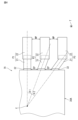
- FIG. 1 is a schematic perspective view partially showing a telescopic device according to a first embodiment of the present disclosure.
- FIG. 2 is a sectional view taken along line II-II in FIG.
- FIG. 3 is a schematic perspective view showing a telescopic device according to a second embodiment of the present disclosure.
- FIG. 4 is a schematic plan view partially showing a telescopic device according to a second embodiment of the present disclosure.
- FIG. 5 is a graph showing the relationship between stress and elongation of the expandable wiring according to the example.
- FIG. 6 is a graph showing the thickness dependence of the relationship between the expansion/contraction rate and the resistance value of the expandable wiring according to the example.
- FIG. 7 is a schematic perspective view partially showing the telescopic device according to the example.
- FIG. 8A is a diagram showing the shape of the paste applied.
- FIG. 8B is a diagram showing the shape of the paste applied.
- FIG. 1 is a schematic perspective view partially showing the telescopic device 1.
- FIG. 2 is a sectional view taken along line II-II in FIG.
- the description of the coating layer is omitted.
- the thickness direction of the stretchable base material is indicated by an arrow T.
- the "direction perpendicular to the main surface of the stretchable base material" described in the claims corresponds to the T direction.
- the direction from the main surface of the stretchable base material where the stretchable wiring is not provided to the main surface of the stretchable base material where the stretchable wire is provided is defined as the upper side.
- the stretchable device 1 includes a stretchable base material 11 having a main surface 111, an electronic component 30 provided on the main surface 111 of the stretchable base material 11, a first stretchable wiring 21 connected to the electronic component 30, and a first stretchable wire 21 connected to the electronic component 30. It includes a second elastic wiring 22 connected to the elastic wiring 21 and a covering layer 50 provided so as to cover the first elastic wiring 21 and the second elastic wiring 22.
- the stretchable device 1 is, for example, attached to a living body and used to measure biological signals.
- on the main surface of the stretchable base material does not refer to an absolute direction such as vertically upward defined in the direction of gravity, but to the outside of the stretchable base material whose boundary is the main surface of the stretchable base material. It refers to the direction toward the outside between the inside and inside. Therefore, “on the main surface of the stretchable base material” is a relative direction determined by the direction of the main surface of the stretchable base material. Furthermore, “above” an element does not only mean a position directly above the element (on), but also a position above the element that is away from the element, that is, a position above the element through another object. It also includes spaced above positions.
- the stretchable base material 11 is a sheet-like or film-like base material made of a stretchable resin material.
- the resin material include thermoplastic polyurethane (TPU).
- TPU thermoplastic polyurethane
- the thickness of the stretchable base material 11 is not particularly limited, but from the viewpoint of not inhibiting the expansion and contraction of the surface of a living body when attached to a living body, it is preferably 1 mm or less, more preferably 100 ⁇ m or less, and 50 ⁇ m or less. It is more preferable that Moreover, it is preferable that the thickness of the stretchable base material 11 is 1 ⁇ m or more.
- the shape of the stretchable base material 11 is not particularly limited. In this embodiment, the stretchable base material 10 is shaped to extend in one direction A when viewed from the thickness direction T.
- the electronic component 30 is, for example, a capacitor component, an inductor component, an IC (semiconductor integrated circuit), or the like.
- the type of electronic component 30 is not particularly limited. Although the shape of the electronic component 30 is not particularly limited, it is a rectangular parallelepiped in this embodiment.
- the electronic component 30 is arranged so that its longitudinal direction is parallel to the extending direction of the stretchable base material 11 (hereinafter referred to as the "A direction"). External electrodes 31 are provided at both ends of the electronic component 30 in the A direction, respectively.
- the first expandable wiring 21 is a member that has a function such as relieving stress applied to the expandable device 1.
- the first stretchable wiring 21 is made of a stretchable conductive material.
- metal foil such as silver, copper, or nickel may be used as the conductive material, or metal powder such as silver, copper, or nickel and elastomeric resin such as epoxy resin, urethane resin, acrylic resin, or silicone resin may be used. You may use the mixture consisting of.
- the first elastic wiring 21 has a larger Young's modulus than the second elastic wiring 22.
- the shape of the first stretchable wiring 21 is not particularly limited, in this embodiment, it has a shape extending in one direction. Specifically, the first stretchable wiring 21 is arranged so that its extending direction is parallel to the A direction.
- a first end 211 of the first expandable wiring 21 in the extending direction is connected to the electronic component 30.
- the first end 211 of the first stretchable wiring 21 in the extending direction is connected to the external electrode 31 on one side of the electronic component 30 via the connecting member 40 .
- the connecting member 40 is, for example, solder, conductive adhesive, or the like.
- the length L1 of the first stretchable wiring 21 in the extending direction is, for example, 0.2 mm or more and 5 mm or less. In this specification, the length L1 does not include the overlapping portion with the second stretchable wiring 22. It is preferable that the width W1 in the direction perpendicular to the extending direction of the first stretchable wiring 21 is, for example, 0.2 mm or more and 3.2 mm or less. It is preferable that the thickness t1 of the first stretchable wiring 21 in the T direction is, for example, 10 ⁇ m or more and 30 ⁇ m or less.
- the second telescopic wiring 22 is a wiring mainly responsible for transmitting and receiving biological signals and the like.
- the second stretchable wiring 22 is made of a stretchable conductive material.
- metal foil such as silver, copper, or nickel may be used as the conductive material, or metal powder such as silver, copper, or nickel and elastomeric resin such as epoxy resin, urethane resin, acrylic resin, or silicone resin may be used.
- elastomeric resin such as epoxy resin, urethane resin, acrylic resin, or silicone resin may be used.
- a mixture consisting of the following may also be used.
- the shape of the second stretchable wiring 22 is not particularly limited, in this embodiment, it has a shape extending in one direction. Specifically, the second stretchable wiring 22 is arranged so that its extending direction is parallel to the A direction.
- the extending direction of the second stretchable wiring 22 is parallel to the extending direction of the first stretchable wiring 21.
- Parallel in this application is not limited to a strict parallel relationship, but also includes a substantial parallel relationship, taking into consideration the range of realistic variations.
- a first end 221 of the second stretchable wiring 22 in the extending direction is connected to a second end 212 of the first stretchable wiring 21 in the extending direction.
- the first end 221 of the second stretchable wiring 22 in the extending direction is stacked on the second end 212 of the first stretchable wiring 21 in the extending direction. It is connected to the second end 212 in the extending direction.
- the present invention is not limited to this, and the second end 212 of the first stretchable wiring 21 in the extending direction is stacked on the first end 221 of the second stretchable wiring 22 in the extending direction, so that the second stretchable wiring 21 may be connected to the first end 221 in the extending direction.
- the length L3 in the A direction of a portion (overlapping portion) 22P of the second stretchable wiring 22 that overlaps with the first stretchable wire 21 is, for example, 0.1 mm or more and 1 mm or less.
- the length L2 of the second stretchable wiring 22 in the extending direction is, for example, three times or more the length L1. In this specification, the length L2 does not include the overlapping portion with the first expandable wiring 21. Further, as shown in FIG. 7, which will be described later, when there are a plurality of electronic components 30 and one second telescoping wiring 22 is connected to the plurality of electronic components 30, L2 is the extension of the second telescoping wiring 22. The length is defined as the midpoint between the electronic components 30 adjacent to each other in the direction. It is preferable that the width W2 of the second stretchable wiring 22 in the direction perpendicular to the extending direction is, for example, 0.2 mm or more and 3.2 mm or less. It is preferable that the thickness t2 of the second stretchable wiring 22 in the T direction is, for example, 10 ⁇ m or more and 30 ⁇ m or less.
- the set of stretchable wiring includes the first stretchable wire 21 connected to the external electrode 31 of the electronic component 30 and the second stretchable wire 22 connected to the first stretchable wire 21.
- the covering layer 50 protects the first elastic wiring 21 and the second elastic wiring 22 from the external environment.
- the covering layer 50 is, for example, potting resin.
- the coating layer 50 is preferably made of a stretchable resin material, such as an ionomer resin, a polyester resin, a styrene resin, an olefin resin, an epoxy resin, a urethane resin, an acrylic resin, or a silicone resin. It is more preferable that Although the covering layer 50 does not need to be provided, it is preferable to cover at least the connecting portion between the first expandable wiring 21 and the electronic component 30.
- the first end 211 of the first elastic wiring 21 in the extending direction is connected to the electronic component 30, and the second end 212 of the first elastic wiring 21 in the extending direction is connected to the second end 211 of the first elastic wiring 21 in the extending direction. Since it is connected to the first end 221 of the stretchable wiring 22 in the extending direction, the end of the electronic component 30 is connected to the first stretchable wiring 21 and the first end when viewed from the direction perpendicular to the main surface 111 of the stretchable base 11. 2 does not overlap with the connection part with the expandable wiring 22.
- the connecting member 40 that connects the electronic component 30 and the first telescopic wiring 21 can also be arranged so as not to overlap the connecting portion between the first telescopic wiring 21 and the second telescopic wiring 22.
- different members can be arranged stepwise from the end of the electronic component 30 toward the second expandable wiring 22.
- the stress that may be concentrated at the connection portion between the electronic component 30 and the first elastic wiring 21 can be dispersed from the end of the electronic component 30 toward the second elastic wiring 22, and the concentration of stress can be alleviated.
- the mechanical strength of the stretchable device 1 can be improved.
- the telescopic device 1 satisfies the following formulas (1) and (2).
- ⁇ Total displacement of the first elastic wiring 21 and the second elastic wiring 22
- L2 Length of the second elastic wiring 22 in the elastic direction
- S1 Cross-sectional area of the first elastic wiring 21 in a cross section perpendicular to the expansion/contraction direction (width W1
- the above ⁇ 1 means the tensile load that acts on the first elastic wiring 21 when the displacement amount ⁇ is applied to the entire first elastic wiring 21 and the second elastic wiring 22.
- the above ⁇ 2 means the tensile load that acts on the second elastic wiring 22 when the displacement amount ⁇ is applied to the entire first elastic wiring 21 and the second elastic wiring 22. That is, satisfying the above formula (1) and formula (2) means that each of the first tensile load ratio and the second tensile load ratio calculated by the following formula is 1 or less.
- First tensile load ratio (Tensile load ⁇ 1 acting on the first elastic wiring 21) / (Allowable stress ⁇ 1 max of the first elastic wiring 21)
- Second tensile load ratio (Tensile load ⁇ 2 acting on the second elastic wiring 22) / (Allowable stress ⁇ 2 max of the second elastic wiring 22)
- the tensile load ⁇ 1 and the tensile load ⁇ 2 are derived by the following formula using the above load F.
- the elastic modulus E1, E2, the lengths L1, L2 in the elastic direction, the cross-sectional areas S1, S2, and the The tensile load ⁇ 1 and the tensile load ⁇ 2 can be adjusted by adjusting the length L3 of the portion where the first elastic wiring 21 and the second elastic wiring 22 overlap each other. Note that when the length of each member of the first elastic wiring 21 and the second elastic wiring 22 in the extending direction is a predetermined length, the portion where the first elastic wiring 21 and the second elastic wiring 22 overlap each other By adjusting the length of , it is possible to adjust the lengths L1 and L2 of the first stretchable wiring 21 and the second stretchable wiring 22 in the stretching direction.
- the allowable stress ⁇ 1 max of the first elastic wiring 21 in the above formula (1) is the stress at the maximum elongation of the first elastic wiring 21.
- the allowable stress ⁇ 1 max of the first elastic wiring 21 can be determined by, for example, the relationship between elongation and stress of the first elastic wiring 21 (stress-strain diagram) after cutting the first elastic wiring 21 to a predetermined length in the extending direction. may be measured to determine the stress at which the first expandable wiring 21 breaks.
- the allowable stress ⁇ 2 max of the second stretchable wiring 22 in the above formula (2) is the stress at the maximum elongation of the second stretchable wiring 22.
- the allowable stress ⁇ 2 max of the second elastic wiring 22 can be determined by, for example, cutting out the second elastic wiring 22 to a predetermined length in the extending direction, and then measuring the relationship between the elongation and stress of the second elastic wiring 22. This may be the stress when the wiring 22 breaks.
- the first tensile load ratio being 1 or less means that the tensile load ⁇ 1 acting on the first elastic wiring 21 is smaller than the allowable stress ⁇ 1 max of the first elastic wiring 21. That is, it means that the selected configuration of the first stretchable wiring 21 means that the first stretchable wiring 21 does not break and the mechanical strength of the first stretchable wiring 21 is sufficient.
- the second tensile load ratio being 1 or less means that the tensile load ⁇ 2 acting on the second elastic wiring 22 is smaller than the allowable stress ⁇ 2 max of the second elastic wiring 22. That is, if the configuration of the second stretchable wiring 22 is selected, it means that the second stretchable wiring 22 does not break and the mechanical strength of the second stretchable wiring 22 is sufficient.
- each of the first tensile load ratio and the second tensile load ratio is 1 or less, so each of the first elastic wiring 21 and the second elastic wiring 22 is broken. It is possible to prevent this from happening. Further, by satisfying the above formulas (1) and (2), the shape and material of the first telescopic wiring 21 and the second telescopic wiring 22 can be determined in accordance with the displacement amount ⁇ . Therefore, the displacement amount ⁇ falls within a range in which the telescopic device 1 does not break.
- connection member 40 further includes a connecting member 40 that connects the electronic component 30 and the first stretchable wiring 21, and when viewed from the direction (T direction) perpendicular to the main surface 111 of the stretchable base material 11, the connecting member 40 is connected to the second stretchable wire 21. It does not overlap with the first end 221 of the wiring 22 in the extending direction. According to this configuration, when the connection member 40 is made of solder, for example, it is possible to suppress the thermal influence on the second expandable wiring 22 during the formation of the connection member 40 .
- the solder erosion resistance of the first elastic wiring 21 is higher than the solder erosion resistance of the second elastic wiring 22.
- Solder erosion is a phenomenon in which metal, etc. in the stretchable wiring melts into the solder, reducing the volume of the stretchable wiring. According to this configuration, when the connection member 40 is solder, the connection reliability between the first expandable wiring 21 and the connection member 40 can be improved.
- a stretchable wire is immersed in molten solder, and a graph showing the relationship between the immersion time and the amount of metal in the melted stretchable wire is created. It can be evaluated that the larger the slope of the graph, the more likely it is to be eaten by solder, that is, the resistance to solder eating is low.
- the solubility (chemical attack) of the first stretchable wiring 21 in the resin is smaller than the solubility (chemical attack) of the second stretchable wiring 22 in the resin.
- the covering layer 50 is made of, for example, a potting resin and covers at least the connecting portion between the electronic component 30 and the first elastic wiring 21, the material of the first elastic wiring 21 is not applied to the coating layer 50. Dissolution can be suppressed.
- the solubility of the stretchable wiring in resin can be evaluated based on, for example, JIS K 7114:2001 (ISO 175:1999).
- This test method involves completely immersing the specimen in a test liquid at a specified temperature and for a specified time. The mass of the test piece is measured before immersion, and after removal from the test solution and, if necessary, after drying. It can be evaluated that the greater the mass change, the greater the solubility in the test liquid (the greater the chemical attack).
- the length L1 of the first stretchable wiring 21 in the extending direction is shorter than the length L2 of the second stretchable wiring 22 in the extending direction. According to this configuration, even if the first elastic wiring 21 is harder than the second elastic wiring 22, the influence on the elasticity of the elastic device 1 can be suppressed.
- the Young's modulus (elastic modulus) of the first elastic wiring 21 is larger than the Young's modulus (elastic modulus) of the second elastic wiring 22.
- the first stretchable wiring 21 can be made harder than the second stretchable wiring 22. Therefore, the hardness can be gradually softened from the end of the electronic component 30 toward the second expandable wiring 22. As a result, stress that may be concentrated at the connection portion between the electronic component 30 and the first expandable wiring 21 can be further alleviated.
- the thickness t1 of the first elastic wiring 21 is larger than the thickness t2 of the second elastic wiring 22. According to this configuration, the solder bite resistance of the first expandable wiring 21 can be further improved. Furthermore, since the allowable stress ⁇ 1 max of the first expandable wiring 21 can be increased, the first tensile load ratio can be further reduced. Furthermore, since the clearance between the electronic component 30 and the stretchable base material 11 can be increased, the ability to fill the clearance with the coating layer 50 can be improved.
- the viscosity of the material for the first elastic wiring 21 is greater than the viscosity of the material for the second elastic wiring 22.
- the thickness t1 of the first stretchable wiring 21 can be made larger than the thickness t2 of the second stretchable wiring 22 more reliably.
- the first stretchable wire 21 is made of a thermosetting material
- the second stretchable wire 22 is made of a thermoplastic material
- the first end 221 of the second stretchable wire 22 in the extending direction is made of the first stretchable wire 22. It is laminated on the second end portion 212 of the wiring 21 in the extending direction. According to this configuration, even when stress is applied to the stretchable device 1, interface peeling between the first stretchable wiring 21 and the second stretchable wire 22 is suppressed, and the mechanical strength of the stretchable device 1 is further improved. Can be done.
- FIG. 3 is a schematic perspective view of the telescopic device 1A.
- FIG. 4 is a schematic plan view partially showing the telescopic device 1A. Specifically, FIG. 4 is a diagram of the lower right portion of the page of FIG. 3 viewed from above.
- the elastic device 1A is different from the elastic device 1 according to the first embodiment in the configurations of electronic components, first elastic wiring, and second elastic wiring.
- the electronic component 30A has a regular square prism shape.
- a plurality of external electrodes 32 are provided on the outer periphery of the lower surface of the electronic component 30A.
- the first elastic wiring 21 and the second elastic wiring 22 each exist in plural numbers, and include a first elastic wiring 21 connected to the electronic component 30A and a second elastic wiring 22 connected to the first elastic wiring 21. There are a plurality of sets of expandable wiring. Specifically, one first elastic wiring 21 is connected to one external electrode 32 of the electronic component 30A, and one second elastic wiring 22 is connected to one first elastic wiring 21. ing. A plurality of sets of stretchable wires each including the one first stretchable wire 21 and the one second stretchable wire 22 exist corresponding to each external electrode 32 .
- each first stretchable wire 21 in the plurality of sets of stretchable wires is radial with respect to the center C of the electronic component 30A.
- the extending direction of the first telescopic wiring 21 in one set of telescopic wiring is different from that in the other set.
- the angle formed by the extending direction of the first stretchable wiring 21 in the set of stretchable wiring is greater than 0° and less than or equal to 90°.
- each first telescopic wiring 21 in the first telescopic wiring group P1, the second telescopic wiring group P2, and the third telescopic wiring group P3 is located at the center of the electronic component 30A. They are arranged on the outer periphery of the electronic component 30A so as to be radial with respect to C.
- the extending direction of the first telescopic wiring 21 in the first telescopic wiring set P1 and the second telescopic wiring set P2 adjacent to each other along the outer periphery of the electronic component 30A the extending direction of the first telescopic wiring 21 in the first telescopic wiring set P1 and the second telescopic wiring
- the angle ⁇ 1 formed by the extending direction of the first elastic wiring 21 in the group P2 is greater than 0° and less than or equal to 90°.
- the extending direction of the first telescoping wiring 21 in the second telescoping wiring set P2 and the third telescoping wiring set P3 adjacent to each other along the outer periphery of the electronic component 30A the extending direction of the first telescoping wiring 21 in the second telescoping wiring set P2 and the third telescoping wiring
- the angle ⁇ 2 formed by the extending direction of the first telescopic wiring 21 in the group P3 is greater than 0° and less than or equal to 90°.
- each second telescoping wiring 22 is The directions are parallel to each other, but they may be arranged at an angle to each other.
- each first telescoping wiring 21 in the plurality of telescoping wiring sets is arranged on the outer periphery of the electronic component 30A so as to be radial with respect to the center C of the electronic component 30A.
- the inter-electrode pitch WP can be made different from the inter-electrode pitch EP.
- the periphery of the electronic component 30A can be covered with the first stretchable wiring 21 which is softer than the electronic component 30A. Therefore, even if tensile stress is applied to the stretchable device 1A, stress that may be concentrated at the connection portion between the electronic component 30A and the first stretchable wiring 21 can be further alleviated. Further, even when tensile stress is applied to the elastic device 1A from any direction, shear deformation at the most affected portion can be reduced, and the durability of the elastic device 1A can be improved.
- each embodiment is an example, and the present disclosure is not limited to each embodiment.
- each drawing is an illustration of the constituent elements, and does not limit the shape.
- partial substitution or combination of the configurations shown in different embodiments is possible.
- Example 1 The elongation against stress was measured for the first stretchable wiring and the second stretchable wiring.
- FIG. 5 is a graph showing the relationship between stress and elongation of the first stretchable wiring and the second stretchable wiring.
- Graph G1 is the result for the first telescopic wiring.
- Graph G2 is the result for the second telescopic wiring.
- the first stretchable wiring broke at about 7% elongation.
- the stress at this time was about 16 MPa. That is, the allowable stress of the first expandable wiring was about 16 MPa.
- the second stretchable wiring broke at about 17% elongation.
- the stress at this time was about 3 MPa. That is, the allowable stress of the second expandable wiring was about 3 MPa.
- FIG. 6 is a graph showing the thickness dependence of the relationship between the expansion/contraction rate and the resistance value of the first expansion/contraction wiring.
- Example 2 The range of tensile load F that can be used without breaking the elastic device was calculated. The calculation below is an example, and the range of tensile load F that can be used without breaking the elastic device depends on the material and shape of the elastic base material, the material and shape of the first and second elastic wiring, and the number of electronic components. and may vary depending on location, etc.
- the tensile load F that can be used without breaking the expansion/contraction device 1 is calculated by the following formula.
- the expansion/contraction ratio ⁇ can be defined, for example, as the ratio of the above-mentioned displacement amount ⁇ to the length of the entire expansion/contraction base material before expansion/contraction.
- Tensile load F E ⁇ ( ⁇ /100) ⁇ S that can be used without breaking the elastic device 1 however, E: Composite elastic modulus (composite elastic modulus) of the elastic base material 11, the first elastic wiring 21, and the second elastic wiring 22 S: Cross-sectional area of the stretchable base material 11 in a cross section perpendicular to the stretch direction
- FIG. 7 is a schematic perspective view partially showing the telescopic device 1B according to the second embodiment.
- a wiring/component group in which the second stretchable wiring 22, the first stretchable wire 21, the electronic component 30, and the first stretchable wire 21 are connected in this order is arranged along the A direction. Connected repeatedly. A plurality of these repeatedly connected wiring/component groups exist in a direction perpendicular to the A direction. In FIG. 7, the directions of expansion and contraction are indicated by arrows.
- the broken line in the area AR in FIG. 7 indicates an imaginary line connecting the midpoints between adjacent electronic components 30. Note that although the area AR is depicted as being square in FIG. 7, the area AR is not necessarily square.
- the center of gravity of the region AR overlaps with the electronic component 30 when viewed from the T direction.
- the area of the region AR is the value obtained by dividing the area of the entire base material by the number of electronic components 30.
- the area of the region AR was 10 mm 2 and the expansion/contraction ratio ⁇ EX was 20%.
- Table 1 shows the elastic modulus (elastic modulus, Young's modulus), cross-sectional area in a cross section perpendicular to the stretching direction, length in the stretching direction, and composite elastic modulus of the stretchable base material, the first stretchable wiring, and the second stretchable wire in the area AR. It was shown to.
- the composite elastic modulus was roughly estimated from the elastic modulus, cross-sectional area, and length of each member.
- the elastic base material was assumed to be thermoplastic polyurethane (TPU).
- TPU thermoplastic polyurethane
- the length of the second stretchable wiring 22 in the stretch direction is the sum of the length L2a and the length L2b.
- the length of the stretchable base material in the stretch direction is the total value of length L1a, length L1b, length L2a, and length L2b.
- Example 3 A paste was used as the material for the first elastic wiring, and the relationship between the viscosity of the paste and the thickness of the first elastic wiring to be formed was investigated. Since the first stretchable wiring has an island shape, it can be printed using a metal mask, and it is possible to use a paste that has increased thixotropy, that is, the viscosity of the paste, by adding a thixotropic agent. The paste was printed using a metal mask to form the first stretchable wiring.
- FIG. 8A is a diagram showing the applied shape of paste M1 to which no thixotropic agent is added.
- FIG. 8B is a diagram showing the application shape of paste M2 containing a thixotropic agent.
- the paste spread and had a thickness of about 25 ⁇ m.
- the paste did not spread and the thickness was about 50 ⁇ m. It was found that the thickness of the first stretchable wiring could be made thicker with paste M2 whose viscosity was increased by adding a thixotropic agent.
- a sample in which the first elastic wiring had a thickness of 10 ⁇ m and a sample in which the first elastic wiring had a thickness of 50 ⁇ m were prepared. Then, for each sample, the solder thickness and the number of reflows were varied, and the resistance to solder eating was evaluated. The thickness of the solder was changed to 20 ⁇ m, 50 ⁇ m, 80 ⁇ m, 110 ⁇ m, and 140 ⁇ m. The number of reflows was changed to 1, 2, 3, 4, and 5 times. Solder eating was observed in the sample in which the first elastic wiring had a thickness of 10 ⁇ m, but no solder eating was observed in the sample in which the first elastic wiring had a thickness of 50 ⁇ m. It has been found that by increasing the thickness of the first stretchable wiring, the resistance to solder eating is improved.
- Example 4 The relationship between the stacking order of the first stretchable wiring and the second stretchable wiring and interfacial peeling was investigated. Specifically, the first end of the second stretchable wiring is laminated on the second end of the first stretchable wiring as shown in FIG. 2, and the second end of the first stretchable wiring It was investigated whether the behavior in which interfacial peeling occurs is different depending on the case where the first end of the second stretchable wiring is laminated on the first end of the second stretchable wiring. A thermosetting material was used as the material for the first stretchable wiring. A thermoplastic material was used as the material for the second stretchable wiring. Table 2 shows the results when the first end of the second stretchable wiring was laminated on the second end of the first stretchable wiring.
- Table 3 shows the results when the second end of the first stretchable wiring was laminated on the first end of the second stretchable wiring.
- the numerical value described as "0.16 N/mm" means the tensile load per unit width at the time of interfacial peeling.
- Cohesive failure is a condition in which the interface between the first and second stretchable wirings does not separate, but the breakage occurs inside either the first or second stretchable wires. It is.
- thermosetting material is used as the material of the first elastic wiring and a thermoplastic material is used as the material of the second elastic wiring
- the first end of the second elastic wiring is placed above the second end of the first elastic wiring. It was found that interfacial delamination is suppressed and mechanical strength is improved when laminated on the substrate.
- the present disclosure includes the following aspects. ⁇ 1> a stretchable base material having a main surface; an electronic component provided on the main surface of the stretchable base material; a first telescopic wiring connected to the electronic component; a second stretchable wiring connected to the first stretchable wiring, A first end in the extending direction of the first stretchable wiring is connected to the electronic component, A stretchable device, wherein a second end of the first stretchable wiring in the extending direction is connected to a first end of the second stretchable wiring in the extending direction.
- the telescopic device according to ⁇ 1> which satisfies the following formula.
- ⁇ 1 ⁇ 0.80 ⁇ allowable stress of first stretchable wiring ⁇ 2 ⁇ 0.80 ⁇ allowable stress of second stretchable wire ⁇ 4> The telescopic device according to ⁇ 2>, which further satisfies the following formula. ⁇ 1 ⁇ 0.50 ⁇ allowable stress of first stretchable wiring ⁇ 2 ⁇ 0.50 ⁇ allowable stress of second stretchable wire ⁇ 5> further comprising a connecting member connecting the electronic component and the first stretchable wiring, Any one of ⁇ 1> to ⁇ 4>, wherein the connection member does not overlap the first end in the extending direction of the second stretchable wiring when viewed from a direction perpendicular to the main surface of the stretchable base material.
- each of the first stretchable wiring and the second stretchable wiring There are a plurality of each of the first stretchable wiring and the second stretchable wiring, There are a plurality of sets of stretchable wiring, each consisting of the first stretchable wire connected to the electronic component and the second stretchable wire connected to the first stretchable wire, from ⁇ 1> to ⁇ 5.
- each first stretchable wire in the plurality of sets of stretchable wires extends around the outer periphery of the electronic component so as to be radial with respect to the center of the electronic component.
- the extending direction of the first stretchable wiring in one set of stretchable wires and the first stretchable wire in the other set of stretchable wires are The telescopic device according to ⁇ 6>, wherein the angle formed by the extending direction of the wiring is greater than 0° and less than or equal to 90°.
- ⁇ 10> The stretchable device according to any one of ⁇ 1> to ⁇ 9>, wherein the length of the first stretchable wiring in the extending direction is shorter than the length of the second stretchable wiring in the extending direction.
- ⁇ 11> The elastic device according to any one of ⁇ 1> to ⁇ 10>, wherein a Young's modulus of the first elastic wiring is larger than a Young's modulus of the second elastic wiring.
- ⁇ 12> The elastic device according to any one of ⁇ 1> to ⁇ 11>, wherein the first elastic wiring has a thickness greater than the second elastic wiring.
- the elastic device according to any one of ⁇ 1> to ⁇ 12>, wherein the viscosity of the material of the first elastic wiring is greater than the viscosity of the material of the second elastic wiring.
- the first stretchable wiring is made of a thermosetting material
- the second stretchable wiring is made of a thermoplastic material
- the first end in the extending direction of the second stretchable wiring is one of ⁇ 1> to ⁇ 13>, which is laminated on the second end in the extending direction of the first stretchable wiring.
- Telescoping device as described.
- Elastic device 11 Elastic base material 111: Main surface 21: First elastic wiring 211: First end of first elastic wiring 212: Second end of first elastic wiring 22: Second elastic Wiring 221: First end of second elastic wiring 222: Second end of second elastic wiring 30, 30A: Electronic components 31, 32: External electrode 40: Connection member 50: Covering layer C: Center L1: Length of the first elastic wiring L2: Length of the second elastic wiring P1, P2, P3: Set of elastic wiring t1: Thickness of the first elastic wiring t2: Thickness of the second elastic wiring W1: Thickness of the second elastic wiring Width of 1st stretch wiring W2: Width of 2nd stretchable wire
Landscapes
- Engineering & Computer Science (AREA)
- Microelectronics & Electronic Packaging (AREA)
- Structure Of Printed Boards (AREA)
Abstract
伸縮デバイス(1)は、主面(111)を有する伸縮基材(11)と、伸縮基材(11)の主面(111)上に設けられた電子部品(30)と、電子部品(30)に接続された第1伸縮配線(21)と、第1伸縮配線(21)に接続された第2伸縮配線(22)と、を備え、第1伸縮配線(21)の延在方向の第1端部(211)が、電子部品(30)に接続され、第1伸縮配線(21)の延在方向の第2端部(212)が、第2伸縮配線(22)の延在方向の第1端部(221)に接続されている。
Description
本開示は、伸縮デバイスに関する。
従来、伸縮デバイスとしては、国際公開第2009/081929号(特許文献1)に記載されたものがある。この伸縮デバイスは、絶縁性基材と、絶縁性基材上に設けられたランドを有した第1導体と、このランド上に設けられた第2導体と、第2導体上にそれぞれ個別に設けられた半田と、当該半田とそれぞれ独立して接する電極部を有する電子部品と、を備える。
従来技術のデバイスでは、電子部品の端部は、第1導体と第2導体の重複領域に重なって配置されている。第2導体上に設けられた半田も当該重複領域に重なって配置されている。
ところで、上記構造の従来技術のデバイスを評価したところ、従来技術のデバイスでは、機械的強度が低いことが分かった。詳細に検討すると、基材として伸縮性を有する伸縮基材を用いる場合、伸長時の応力は、半田などの接続部材と配線の界面の近傍に最も集中し得ることが分かった。このため、従来技術のデバイスでは、配線の断線や、基材と配線の界面剥離などが発生するおそれがあることが分かった。
そこで、本開示の目的は、機械的強度を向上させることができる伸縮デバイスを提供することにある。
上記目的を達成するために本開示の一態様に係る伸縮デバイスは、
主面を有する伸縮基材と、
前記伸縮基材の前記主面上に設けられた電子部品と、
前記電子部品に接続された第1伸縮配線と、
前記第1伸縮配線に接続された第2伸縮配線と、を備え、
前記第1伸縮配線の延在方向の第1端部が、前記電子部品に接続され、
前記第1伸縮配線の延在方向の第2端部が、前記第2伸縮配線の延在方向の第1端部に接続されている。
主面を有する伸縮基材と、
前記伸縮基材の前記主面上に設けられた電子部品と、
前記電子部品に接続された第1伸縮配線と、
前記第1伸縮配線に接続された第2伸縮配線と、を備え、
前記第1伸縮配線の延在方向の第1端部が、前記電子部品に接続され、
前記第1伸縮配線の延在方向の第2端部が、前記第2伸縮配線の延在方向の第1端部に接続されている。
本開示の一態様に係る伸縮デバイスによれば、機械的強度を向上させることができる。
以下、本開示の実施形態について、図面を用いて詳細に説明する。各々の実施形態では、その実施形態以前に説明した点と異なる点について主に説明する。特に、同様の構成による同様の作用効果については実施形態ごとには逐次言及しない。以下の実施形態における構成要素のうち、独立請求項に記載されていない構成要素については、任意の構成要素として説明される。また、図面に示される構成要素の大きさおよび大きさの比は、必ずしも厳密ではない。また、各図において、実質的に同一の構成に対しては同一の符号を付しており、重複する説明は省略又は簡略化する場合がある。
[第1実施形態]
(全体構成)
図1および図2を参照しながら、第1実施形態に係る伸縮デバイス1の全体構成について説明する。図1は、伸縮デバイス1を部分的に示した模式斜視図である。図2は、図1のII-II断面図である。なお、図1では、被覆層の記載を省略している。
(全体構成)
図1および図2を参照しながら、第1実施形態に係る伸縮デバイス1の全体構成について説明する。図1は、伸縮デバイス1を部分的に示した模式斜視図である。図2は、図1のII-II断面図である。なお、図1では、被覆層の記載を省略している。
本明細書の図面では、伸縮基材の厚み方向を矢印Tで示している。特許請求の範囲に記載の「伸縮基材の主面に直交する方向」は、T方向に相当する。また、本明細書では、T方向のうち、伸縮配線が設けられていない伸縮基材の主面から、伸縮配線が設けられている伸縮基材の主面に向かう方向を上側とする。
伸縮デバイス1は、主面111を有する伸縮基材11と、伸縮基材11の主面111上に設けられた電子部品30と、電子部品30に接続された第1伸縮配線21と、第1伸縮配線21に接続された第2伸縮配線22と、第1伸縮配線21および第2伸縮配線22を覆うように設けられた被覆層50と、を備える。伸縮デバイス1は、例えば、生体に貼り付けられて、生体信号を測定するために用いられる。
ここで、「伸縮基材の主面上」とは、重力方向に規定される鉛直上方のような絶対的な一方向ではなく、当該伸縮基材の主面を境界とする伸縮基材の外側と内側とのうち、外側に向かう方向を指す。したがって、「伸縮基材の主面上」とは伸縮基材の主面の向きによって定まる相対的な方向である。また、ある要素に対して「上」には、当該要素と接する直上の位置(on)だけではなく、当該要素とは離れた上方、すなわち当該要素上の他の物体を介した上側の位置や間隔を空けた上側の位置(above)も含む。
伸縮基材11は、伸縮性を有する樹脂材料から構成されるシート状あるいはフィルム状の基材である。樹脂材料としては、例えば、熱可塑性ポリウレタン(Thermoplastic Polyurethane:TPU)等が挙げられる。伸縮基材11の厚さは特に限定されないが、生体に貼り付けた際に生体表面の伸縮を阻害しない観点からは、1mm以下であることが好ましく、100μm以下であることがより好ましく、50μm以下であることがさらに好ましい。また、伸縮基材11の厚さは、1μm以上であることが好ましい。伸縮基材11の形状は、特に限定されない。この実施形態では、伸縮基材10は、厚み方向Tからみて、1方向Aに延在する形状にされている。
電子部品30は、例えば、コンデンサ部品、インダクタ部品、IC(半導体集積回路)などである。電子部品30の種類は、特に限定されない。電子部品30の形状は、特に限定されないが、この実施形態では直方体状である。電子部品30は、長手方向が伸縮基材11の延在方向(以下、「A方向」という。)と平行になるように配置されている。電子部品30のA方向の両端部には、外部電極31がそれぞれ設けられている。
第1伸縮配線21は、伸縮デバイス1に負荷される応力を緩和するなどの機能を有する部材である。第1伸縮配線21は、伸縮性を有する導電性材料で形成される。導電性材料には、例えば、銀、銅、ニッケルなどの金属箔を用いてもよく、銀、銅、ニッケルなどの金属粉とエポキシ樹脂、ウレタン樹脂、アクリル樹脂およびシリコーン樹脂などのエラストマ系樹脂とからなる混合物を用いてもよい。第1伸縮配線21は、第2伸縮配線22よりヤング率が大きいことが好ましい。第1伸縮配線21の形状は特に限定されないが、この実施形態では、1方向に延在する形状にされている。具体的に述べると、第1伸縮配線21は、延在方向がA方向と平行になるようにされている。
第1伸縮配線21の延在方向の第1端部211は、電子部品30に接続されている。具体的に述べると、第1伸縮配線21の延在方向の第1端部211は、接続部材40を介して、電子部品30の一方側の外部電極31に接続されている。接続部材40は、例えば半田、導電性接着剤などである。
第1伸縮配線21の延在方向の長さL1は、例えば0.2mm以上5mm以下であることが好ましい。本明細書では、長さL1は、第2伸縮配線22との重複部分は含まない。第1伸縮配線21の延在方向に直交する方向の幅W1は、例えば0.2mm以上3.2mm以下であることが好ましい。第1伸縮配線21のT方向の厚みt1は、例えば10μm以上30μm以下であることが好ましい。
第2伸縮配線22は、生体信号などの送受信を主に担う配線である。第2伸縮配線22は、伸縮性を有する導電性材料で形成される。導電性材料には、例えば、銀、銅、ニッケルなどの金属箔を用いてもよく、銀、銅、ニッケルなどの金属粉とエポキシ樹脂、ウレタン樹脂、アクリル樹脂およびシリコーン樹脂などのエラストマ系樹脂とからなる混合物を用いてもよい。第2伸縮配線22の形状は特に限定されないが、この実施形態では、1方向に延在する形状にされている。具体的に述べると、第2伸縮配線22は、延在方向がA方向と平行になるようにされている。すなわち、第2伸縮配線22の延在方向は、第1伸縮配線21の延在方向と平行である。本願における「平行」とは、厳密な平行関係に限定されず、現実的なばらつきの範囲を考慮し、実質的な平行関係も含む。
第2伸縮配線22の延在方向の第1端部221は、第1伸縮配線21の延在方向の第2端部212に接続されている。具体的に述べると、第2伸縮配線22の延在方向の第1端部221は、第1伸縮配線21の延在方向の第2端部212上に積層されて、第1伸縮配線21の延在方向の第2端部212に接続されている。しかしこれに限定されず、第1伸縮配線21の延在方向の第2端部212が、第2伸縮配線22の延在方向の第1端部221上に積層されて、第2伸縮配線22の延在方向の第1端部221に接続されていてもよい。第2伸縮配線22のうちの第1伸縮配線21と重なっている部分(重複部分)22PのA方向の長さL3は、例えば0.1mm以上1mm以下であることが好ましい。
第2伸縮配線22の延在方向の長さL2は、例えば長さL1の3倍以上であることが好ましい。本明細書では、長さL2は、第1伸縮配線21との重複部分は含まない。また、後述する図7に示すように、電子部品30が複数存在し、1つの第2伸縮配線22が複数の電子部品30に接続されている場合、L2は、第2伸縮配線22の延在方向に隣り合う電子部品30の間の中点までの長さとする。第2伸縮配線22の延在方向に直交する方向の幅W2は、例えば0.2mm以上3.2mm以下であることが好ましい。第2伸縮配線22のT方向の厚みt2は、例えば10μm以上30μm以下であることが好ましい。
この実施形態では、電子部品30の外部電極31に接続された第1伸縮配線21と、当該第1伸縮配線21に接続された第2伸縮配線22と、から構成される伸縮配線の組は、電子部品30のA方向の両端部に設けられている2つの外部電極31の各々に対応して2組存在する。
被覆層50は、第1伸縮配線21および第2伸縮配線22を外部環境から保護する。被覆層50は、例えばポッティング樹脂である。被覆層50は、伸縮性を有する樹脂材料であることが好ましく、例えば、アイオノマー樹脂、ポリエステル樹脂、スチレン樹脂、オレフィン樹脂、エポキシ樹脂、ウレタン樹脂、アクリル樹脂又はシリコーン樹脂であることが好ましく、ウレタン樹脂であることがより好ましい。なお、被覆層50は、設けられていなくてもよいが、第1伸縮配線21と電子部品30との接続部分を少なくとも覆うことが好ましい。
伸縮デバイス1によれば、第1伸縮配線21の延在方向の第1端部211が、電子部品30に接続され、第1伸縮配線21の延在方向の第2端部212が、第2伸縮配線22の延在方向の第1端部221に接続されているため、伸縮基材11の主面111に直交する方向からみて、電子部品30の端部は、第1伸縮配線21と第2伸縮配線22との接続部分とは重ならない。さらに言えば、電子部品30と第1伸縮配線21とを接続する接続部材40も、第1伸縮配線21と第2伸縮配線22との接続部分と重ならないように配置できる。これにより、電子部品30の端部から第2伸縮配線22に向かって、段階的に異なる部材を配置できる。その結果、電子部品30と第1伸縮配線21との接続部分に集中し得る応力を、電子部品30の端部から第2伸縮配線22に向かって分散させて、当該応力の集中を緩和できる。その結果、伸縮デバイス1の機械的強度を向上させることができる。
(引張荷重比)
伸縮デバイス1では、下記式(1)および式(2)を満たすことが好ましい。なお、以下の説明では、伸縮方向は、A方向と平行であるとする。
σ1≦第1伸縮配線の許容応力σ1max ・・・(1)
σ2≦第2伸縮配線の許容応力σ2max ・・・(2)
ただし、
σ1=(δ×E1×S2×E2)/(L1×S2×E2+L2×S1×E1) ・・・(3)
σ2=(δ×E1×S1×E2)/(L1×S2×E2+L2×S1×E1) ・・・(4)
δ:第1伸縮配線21および第2伸縮配線22の全体の変位量
L1:伸縮方向(A方向)における第1伸縮配線21の長さ
L2:伸縮方向における第2伸縮配線22の長さ
S1:伸縮方向に直交する断面における第1伸縮配線21の断面積(第1伸縮配線21の幅W1×厚みt1)
S2:伸縮方向に直交する断面における第2伸縮配線22の断面積(第2伸縮配線22の幅W2×厚みt2)
E1:第1伸縮配線21の弾性係数
E2:第2伸縮配線22の弾性係数
上記σ1は、第1伸縮配線21および第2伸縮配線22の全体に変位量δが与えられたときの第1伸縮配線21に作用する引張荷重を意味する。上記σ2は、第1伸縮配線21および第2伸縮配線22の全体に変位量δが与えられたときの第2伸縮配線22に作用する引張荷重を意味する。すなわち、上記式(1)および式(2)を満たすことは、下記式で計算される第1引張荷重比および第2引張荷重比の各々が、1以下であることを意味する。
第1引張荷重比=(第1伸縮配線21に作用する引張荷重σ1)/(第1伸縮配線21の許容応力σ1max)
第2引張荷重比=(第2伸縮配線22に作用する引張荷重σ2)/(第2伸縮配線22の許容応力σ2max)
第1引張荷重比=(第1伸縮配線21に作用する引張荷重σ1)/(第1伸縮配線21の許容応力σ1max)
第2引張荷重比=(第2伸縮配線22に作用する引張荷重σ2)/(第2伸縮配線22の許容応力σ2max)
ここで、引張荷重σ1および引張荷重σ2の算出式である上記式(3)および式(4)の導出について説明する。第1伸縮配線21および第2伸縮配線22の全体に変位量δを与えたとき、第1伸縮配線21および第2伸縮配線22に加わる荷重Fは、下記式で表される。
F=δ/[{L1/(E1×S1)}+{L2/(E2×S2)}]
F=δ/[{L1/(E1×S1)}+{L2/(E2×S2)}]
引張荷重σ1および引張荷重σ2は、上記荷重Fを用いて、下記式により導出される。
σ1=F/S1=(δ/S1)×{(E1×S1×E2×S2)/(L1×S2×E2+L2×S1×E1)}=(δ×E1×S2×E2)/(L1×S2×E2+L2×S1×E1)
σ2=F/S2=(δ/S2)×{(E1×S1×E2×S2)/(L1×S2×E2+L2×S1×E1)}=(δ×E1×S1×E2)/(L1×S2×E2+L2×S1×E1)
σ1=F/S1=(δ/S1)×{(E1×S1×E2×S2)/(L1×S2×E2+L2×S1×E1)}=(δ×E1×S2×E2)/(L1×S2×E2+L2×S1×E1)
σ2=F/S2=(δ/S2)×{(E1×S1×E2×S2)/(L1×S2×E2+L2×S1×E1)}=(δ×E1×S1×E2)/(L1×S2×E2+L2×S1×E1)
上記式(3)および式(4)から分かるように、第1伸縮配線21および第2伸縮配線22の、弾性率E1,E2、伸縮方向における長さL1,L2、断面積S1,S2および第1伸縮配線21と第2伸縮配線22が相互に重なる部分の長さL3を調整することにより、引張荷重σ1および引張荷重σ2を調整することができる。なお、第1伸縮配線21および第2伸縮配線22の各部材の延在方向の長さが予め決められた長さであるとき、第1伸縮配線21と第2伸縮配線22が相互に重なる部分の長さを調整することにより、第1伸縮配線21および第2伸縮配線22の伸縮方向の長さL1,L2を調整することができる。
なお、上記引張荷重σ1の計算および上記引張荷重σ2の計算は、2組の伸縮配線の組のうちの一方の組について示したが、他方の組についても同様である。すなわち、2組の伸縮配線の組のそれぞれについて、δ、L1、L2、S1、S2、E1およびE2を規定できる。
上記式(1)における第1伸縮配線21の許容応力σ1maxは、第1伸縮配線21の最大伸びにおける応力である。第1伸縮配線21の許容応力σ1maxは、例えば、第1伸縮配線21を延在方向に所定長さで切り出した後に、第1伸縮配線21の伸びと応力の関係(応力-ひずみ線図)を測定し、第1伸縮配線21が破断するときの応力とすればよい。上記式(2)における第2伸縮配線22の許容応力σ2maxは、第2伸縮配線22の最大伸びにおける応力である。第2伸縮配線22の許容応力σ2maxは、例えば、第2伸縮配線22を延在方向に所定長さで切り出した後に、第2伸縮配線22の伸びと応力の関係を測定し、第2伸縮配線22が破断するときの応力とすればよい。
第1引張荷重比が1以下であるとは、第1伸縮配線21に作用する引張荷重σ1が、第1伸縮配線21の許容応力σ1maxよりも小さいことを意味する。すなわち、選択した第1伸縮配線21の構成であれば、第1伸縮配線21が破断せずに、第1伸縮配線21の機械的強度が十分であることを意味する。同様に、第2引張荷重比が1以下であるとは、第2伸縮配線22に作用する引張荷重σ2が、第2伸縮配線22の許容応力σ2maxよりも小さいことを意味する。すなわち、選択した第2伸縮配線22の構成であれば、第2伸縮配線22が破断せずに、第2伸縮配線22の機械的強度が十分であることを意味する。
上記式(1)および式(2)を満たすことにより、第1引張荷重比および第2引張荷重比の各々が1以下であるため、第1伸縮配線21および第2伸縮配線22の各々が破断されることを抑制できる。また、上記式(1)および式(2)を満たすようにすることで、変位量δに対応した第1伸縮配線21および第2伸縮配線22の形状および材質を決定することができる。そのため、変位量δは、伸縮デバイス1が破断しない範囲となる。
より好ましくは、さらに下記式を満たす。
σ1≦0.80×第1伸縮配線21の許容応力σ1max
σ2≦0.80×第2伸縮配線22の許容応力σ2max
この構成によれば、より確実に第1伸縮配線21および第2伸縮配線22の破断を抑制できる。
σ1≦0.80×第1伸縮配線21の許容応力σ1max
σ2≦0.80×第2伸縮配線22の許容応力σ2max
この構成によれば、より確実に第1伸縮配線21および第2伸縮配線22の破断を抑制できる。
さらにより好ましくは、さらに下記式を満たす。
σ1≦0.50×第1伸縮配線21の許容応力σ1max
σ2≦0.50×第2伸縮配線22の許容応力σ2max
この構成によれば、さらにより確実に第1伸縮配線21および第2伸縮配線22の破断を抑制できる。
σ1≦0.50×第1伸縮配線21の許容応力σ1max
σ2≦0.50×第2伸縮配線22の許容応力σ2max
この構成によれば、さらにより確実に第1伸縮配線21および第2伸縮配線22の破断を抑制できる。
(その他の好ましい構成)
好ましくは、電子部品30と第1伸縮配線21とを接続する接続部材40をさらに備え、伸縮基材11の主面111に直交する方向(T方向)からみて、接続部材40は、第2伸縮配線22の延在方向の第1端部221と重ならない。この構成によれば、例えば接続部材40が半田の場合に、接続部材40の形成時の熱影響を第2伸縮配線22に与えることを抑制できる。
好ましくは、電子部品30と第1伸縮配線21とを接続する接続部材40をさらに備え、伸縮基材11の主面111に直交する方向(T方向)からみて、接続部材40は、第2伸縮配線22の延在方向の第1端部221と重ならない。この構成によれば、例えば接続部材40が半田の場合に、接続部材40の形成時の熱影響を第2伸縮配線22に与えることを抑制できる。
好ましくは、第1伸縮配線21のはんだ喰われ耐性は、第2伸縮配線22のはんだ喰われ耐性よりも高い。はんだ喰われとは、伸縮配線中の金属などが半田に溶け出して、伸縮配線の体積が減少する現象である。この構成によれば、接続部材40が半田である場合に、第1伸縮配線21と接続部材40との接続信頼性を向上させることができる。
はんだ喰われ耐性の評価方法の一例としては、例えば、溶融した半田に伸縮配線を浸漬させて、浸漬時間と溶解した伸縮配線中の金属の量との関係を示すグラフを作成する。そして、グラフの傾きが大きいほどはんだ喰われしやすい、すなわち、はんだ喰われ耐性が低いと評価することができる。
好ましくは、第1伸縮配線21の樹脂に対する溶解性(化学的アタック)は、第2伸縮配線22の樹脂に対する溶解性(化学的アタック)よりも小さい。この構成によれば、被覆層50が、例えばポッティング樹脂であり、電子部品30と第1伸縮配線21との接続部分を少なくとも覆っている場合でも、第1伸縮配線21の材料が被覆層50に溶解することを抑制できる。
伸縮配線の樹脂に対する溶解性の評価は、例えばJIS K 7114:2001(ISO 175:1999)に基づいて行うことができる。この試験方法は、規定温度および規定の時間で試験液中に試験片を完全に浸漬する。浸漬前、および、試験液から取り出し後必要に応じて乾燥後に、試験片の質量を測定する。質量変化が大きいほど試験液に対する溶解性が大きい(化学的アタックが大きい)と評価することができる。
好ましくは、第1伸縮配線21の延在方向の長さL1は、第2伸縮配線22の延在方向の長さL2よりも短い。この構成によれば、第1伸縮配線21が第2伸縮配線22よりも硬い場合でも、伸縮デバイス1の伸縮性に与える影響を抑制できる。
好ましくは、第1伸縮配線21のヤング率(弾性係数)は、第2伸縮配線22のヤング率(弾性係数)よりも大きい。この構成によれば、第1伸縮配線21を第2伸縮配線22よりも硬くできる。そのため、電子部品30の端部から第2伸縮配線22に向かって、段階的に硬さを柔らかくできる。その結果、電子部品30と第1伸縮配線21との接続部分に集中し得る応力をさらに緩和できる。
好ましくは、第1伸縮配線21の厚みt1は、第2伸縮配線22の厚みt2よりも大きい。この構成によれば、第1伸縮配線21のはんだ喰われ耐性をさらに向上させることができる。また、第1伸縮配線21の許容応力σ1maxを大きくできるため、第1引張荷重比をさらに低減できる。また、電子部品30と伸縮基材11との間のクリアランスを大きくできるため、当該クリアランスへの被覆層50の充填性を高めることができる。
好ましくは、第1伸縮配線21の材料の粘度は、第2伸縮配線22の材料の粘度よりも大きい。この構成によれば、より確実に、第1伸縮配線21の厚みt1を第2伸縮配線22の厚みt2よりも大きくできる。
好ましくは、第1伸縮配線21は、熱硬化性材料からなり、第2伸縮配線22は、熱可塑性材料からなり、第2伸縮配線22の延在方向の第1端部221は、第1伸縮配線21の延在方向の第2端部212上に積層されている。この構成によれば、伸縮デバイス1に応力が負荷された場合でも、第1伸縮配線21と第2伸縮配線22の間の界面剥離を抑制し、伸縮デバイス1の機械的強度をさらに向上させることができる。
[第2実施形態]
以下、図3および図4を参照して第2実施形態に係る伸縮デバイス1Aについて説明する。図3は、伸縮デバイス1Aの模式斜視図である。図4は、伸縮デバイス1Aを部分的に示す模式平面図である。具体的に述べると、図4は、図3の紙面右下の部分を上方からみたときの図である。伸縮デバイス1Aは、第1実施形態に係る伸縮デバイス1と比較して、電子部品、第1伸縮配線および第2伸縮配線の各構成が異なる。
以下、図3および図4を参照して第2実施形態に係る伸縮デバイス1Aについて説明する。図3は、伸縮デバイス1Aの模式斜視図である。図4は、伸縮デバイス1Aを部分的に示す模式平面図である。具体的に述べると、図4は、図3の紙面右下の部分を上方からみたときの図である。伸縮デバイス1Aは、第1実施形態に係る伸縮デバイス1と比較して、電子部品、第1伸縮配線および第2伸縮配線の各構成が異なる。
図3および図4に示すように、この実施形態では、電子部品30Aの形状は、正四角柱にされている。電子部品30Aの下面の外周には、複数の外部電極32が設けられている。
第1伸縮配線21および第2伸縮配線22は、それぞれ複数存在し、電子部品30Aに接続された第1伸縮配線21と、当該第1伸縮配線21に接続された第2伸縮配線22と、から構成される伸縮配線の組は、複数存在する。具体的に述べると、電子部品30Aの1つの外部電極32には、1つの第1伸縮配線21が接続され、当該1つの第1伸縮配線21には、1つの第2伸縮配線22が接続されている。そして、当該1つの第1伸縮配線21と当該1つの第2伸縮配線22とから構成される伸縮配線の組が、各外部電極32に対応して複数存在している。
上記構成によれば、上記伸縮配線の組が複数存在するため、電子部品30Aと第1伸縮配線21との接続部分に集中し得る応力をさらに緩和でき、伸縮デバイス1Aの機械的強度をさらに向上させることができる。
好ましくは、伸縮基材11の主面111に直交する方向(T方向)からみて、複数の上記伸縮配線の組における各第1伸縮配線21は、電子部品30Aの中心Cに対して放射状となるように、電子部品30Aの外周に配置され、電子部品30Aの外周に沿って隣り合う2つの伸縮配線の組において、一方の伸縮配線の組における第1伸縮配線21の延在方向と、他方の伸縮配線の組における第1伸縮配線21の延在方向と、のなす角は、0°超90°以下である。
具体的に述べると、図4に示すように、第1伸縮配線の組P1、第2伸縮配線の組P2および第3伸縮配線の組P3における各第1伸縮配線21は、電子部品30Aの中心Cに対して放射状となるように、電子部品30Aの外周に配置されている。電子部品30Aの外周に沿って隣り合う第1伸縮配線の組P1および第2伸縮配線の組P2において、第1伸縮配線の組P1における第1伸縮配線21の延在方向と、第2伸縮配線の組P2における第1伸縮配線21の延在方向と、のなす角θ1は、0°超90°以下である。電子部品30Aの外周に沿って隣り合う第2伸縮配線の組P2および第3伸縮配線の組P3において、第2伸縮配線の組P2における第1伸縮配線21の延在方向と、第3伸縮配線の組P3における第1伸縮配線21の延在方向と、のなす角θ2は、0°超90°以下である。
なお、この実施形態では、T方向からみたときの電子部品30Aの外周の一辺に設けられている外部電極32に接続された複数の第2伸縮配線22において、各第2伸縮配線22の延在方向は、互いに平行であるが、互いに傾いて配置されていてもよい。
上記構成によれば、複数の上記伸縮配線の組における各第1伸縮配線21は、電子部品30Aの中心Cに対して放射状となるように、電子部品30Aの外周に配置されているため、配線間ピッチWPを電極間ピッチEPと異ならせることができる。また、電子部品30Aの周囲を、電子部品30Aよりも柔らかい第1伸縮配線21で覆うようにすることができる。このため、伸縮デバイス1Aに引張応力が加えられた場合でも、電子部品30Aと第1伸縮配線21との接続部分に集中し得る応力をさらに緩和できる。また、伸縮デバイス1Aにいかなる方向から引張応力が加えられた場合でも、最も影響を受ける箇所のせん断変形を小さくでき、伸縮デバイス1Aの耐久性を向上させることができる。
なお、各実施形態は例示であり、本開示は各実施形態に限定されるものではない。また、各図面は構成要素の例示であって、形状を限定するものではない。また、異なる実施形態で示した構成の部分的な置換又は組み合わせが可能である。
前記実施形態では、電子部品に接続された第1伸縮配線と、当該第1伸縮配線に接続された第2伸縮配線との組は、複数存在したが、伸縮配線の組は、少なくとも1組存在すればよい。
(実施例1)
第1伸縮配線および第2伸縮配線について応力に対する伸びを測定した。図5は、第1伸縮配線および第2伸縮配線の応力に対する伸びの関係を示すグラフである。グラフG1は、第1伸縮配線についての結果である。グラフG2は、第2伸縮配線についての結果である。
第1伸縮配線および第2伸縮配線について応力に対する伸びを測定した。図5は、第1伸縮配線および第2伸縮配線の応力に対する伸びの関係を示すグラフである。グラフG1は、第1伸縮配線についての結果である。グラフG2は、第2伸縮配線についての結果である。
図5に示すように、第1伸縮配線は、7%程度の伸びで破断した。この際の応力は、16MPa程度であった。すなわち、第1伸縮配線の許容応力は16MPa程度であった。第2伸縮配線は、17%程度の伸びで破断した。この際の応力は、3MPa程度であった。すなわち、第2伸縮配線の許容応力は3MPa程度であった。
第1伸縮配線の厚みと、第1伸縮配線が破断するまでの伸縮率と、の関係を測定した。図6は、第1伸縮配線の伸縮率と抵抗値の関係の厚み依存性を示すグラフである。
図6に示すように、第1伸縮配線の厚みが大きくなるに従って、破断するまでの伸縮率が大きくなることが分かった。第1伸縮配線の厚みが大きくなるに従って、第1伸縮配線に作用する引張荷重が低減し、第1引張荷重比が低減したためと考えられる。
(実施例2)
伸縮デバイスが破断することなく使用できる引張荷重Fの範囲について計算した。なお、以下の計算は一例であり、伸縮デバイスが破断することなく使用できる引張荷重Fの範囲は、伸縮基材の材質および形状、第1,第2伸縮配線の材質および形状、電子部品の個数および配置などによって変わり得る。
伸縮デバイスが破断することなく使用できる引張荷重Fの範囲について計算した。なお、以下の計算は一例であり、伸縮デバイスが破断することなく使用できる引張荷重Fの範囲は、伸縮基材の材質および形状、第1,第2伸縮配線の材質および形状、電子部品の個数および配置などによって変わり得る。
伸縮率をε%と想定した場合、伸縮デバイス1が破断することなく使用できる引張荷重Fは、下記式で計算される。伸縮率εは、例えば、伸縮前の伸縮基材全体の長さに対する、上述した変位量δの割合として定義できる。
伸縮デバイス1が破断することなく使用できる引張荷重F=E×(ε/100)×S
ただし、
E:伸縮基材11、第1伸縮配線21および第2伸縮配線22の合成弾性率(合成弾性係数)
S:伸縮方向に直交する断面における伸縮基材11の断面積
伸縮デバイス1が破断することなく使用できる引張荷重F=E×(ε/100)×S
ただし、
E:伸縮基材11、第1伸縮配線21および第2伸縮配線22の合成弾性率(合成弾性係数)
S:伸縮方向に直交する断面における伸縮基材11の断面積
図7は、実施例2に係る伸縮デバイス1Bを部分的に示す模式斜視図である。図7に示すように、伸縮デバイス1Bでは、第2伸縮配線22、第1伸縮配線21、電子部品30および第1伸縮配線21がこの順に接続された配線/部品群が、A方向に沿って繰り返し接続されている。そして、この繰り返し接続された配線/部品群が、A方向に直交する方向に複数存在している。図7では、伸縮方向を矢印で示した。
図7の領域ARの破線は、隣り合う電子部品30の間の中点を結んだ仮想線を示している。なお、図7では、領域ARは正方形であるように描かれているが、領域ARは正方形であるとは限らない。領域ARの重心は、T方向からみて、電子部品30と重なる。領域ARの面積は、基材全体の面積を電子部品30の個数で除した値である。領域ARがεEXの伸縮率で伸縮したとき、この占有範囲の合成弾性率をEEX、伸縮方向に直交する断面における断面積をSEXとすると、この占有範囲の荷重dFは、下記式で計算される。
dF=EEX×εEX×SEX
dF=EEX×εEX×SEX
領域ARの面積を10mm2、伸縮率εEXを20%と想定した。領域ARにおける、伸縮基材、第1伸縮配線および第2伸縮配線の弾性率(弾性係数、ヤング率)、伸縮方向に直交する断面における断面積、伸縮方向の長さおよび合成弾性率を表1に示した。合成弾性率は、各部材の弾性率、断面積および長さから概算した。伸縮基材は、熱可塑性ポリウレタン(TPU)を想定した。図7において、第1伸縮配線21の伸縮方向の長さは、長さL1aと長さL1bの合計値である。第2伸縮配線22の伸縮方向の長さは、長さL2aと長さL2bの合計値である。伸縮基材の伸縮方向の長さは、長さL1aと長さL1bと長さL2aと長さL2bの合計値である。

断面積SEXを伸縮基材の断面積と近似したとき、荷重dFは下記のように計算される。
dF=EEX×εEX×SEX=14MPa×0.2×(4×10-1mm2)=1.12N
伸縮デバイス1Bの全体の面積が100mm2の場合、荷重は10倍となるため、伸縮デバイスが破断することなく使用できる引張荷重Fは最大10Nと計算される。
dF=EEX×εEX×SEX=14MPa×0.2×(4×10-1mm2)=1.12N
伸縮デバイス1Bの全体の面積が100mm2の場合、荷重は10倍となるため、伸縮デバイスが破断することなく使用できる引張荷重Fは最大10Nと計算される。
(実施例3)
第1伸縮配線の材料としてペーストを使用し、ペーストの粘度と、形成される第1伸縮配線の厚みと、の関係を調査した。第1伸縮配線の形状は島状のため、メタルマスクを用いて印刷することができ、チクソ剤添加によりチクソ性、すなわちペーストの粘度を上げたペーストを使用することができる。メタルマスクを用いてペーストを印刷して、第1伸縮配線を形成した。
第1伸縮配線の材料としてペーストを使用し、ペーストの粘度と、形成される第1伸縮配線の厚みと、の関係を調査した。第1伸縮配線の形状は島状のため、メタルマスクを用いて印刷することができ、チクソ剤添加によりチクソ性、すなわちペーストの粘度を上げたペーストを使用することができる。メタルマスクを用いてペーストを印刷して、第1伸縮配線を形成した。
図8Aは、チクソ剤を添加していないペーストM1の塗布形状を示した図である。図8Bは、チクソ剤を添加したペーストM2の塗布形状を示した図である。図8Aに示すように、チクソ剤を添加していないペーストM1では、ペーストが広がり、厚みは25μm程度であった。図8Bに示すように、チクソ剤を添加したペーストM2では、ペーストが広がらず、厚みは50μm程度であった。チクソ剤を添加して粘度を高めたペーストM2では、第1伸縮配線の厚みを厚くできることが分かった。
また、第1伸縮配線の厚みが10μmのサンプルと第1伸縮配線の厚みが50μmのサンプルとを準備した。そして、各サンプルについて、半田の厚みおよびリフロー回数を種々変更して、はんだ喰われ耐性を評価した。半田の厚みは、20μm、50μm、80μm、110μmおよび140μmに変更した。リフロー回数は、1回、2回、3回、4回および5回に変更した。第1伸縮配線の厚みが10μmのサンプルでは、はんだ喰われが確認されたが、第1伸縮配線の厚みが50μmのサンプルでは、はんだ喰われが確認されなかった。第1伸縮配線の厚みを大きくすることにより、はんだ喰われ耐性が向上することが分かった。
(実施例4)
第1伸縮配線と第2伸縮配線の積層順番と界面剥離との関係を調査した。具体的に述べると、図2に示したような第2伸縮配線の第1端部が第1伸縮配線の第2端部上に積層されている場合と、第1伸縮配線の第2端部が第2伸縮配線の第1端部上に積層されている場合とで、界面剥離が発生する挙動が異なるかどうかを調査した。第1伸縮配線の材料は、熱硬化性材料を用いた。第2伸縮配線の材料は、熱可塑性材料を用いた。表2は、第2伸縮配線の第1端部を第1伸縮配線の第2端部上に積層したときの結果を示した。表3は、第1伸縮配線の第2端部を第2伸縮配線の第1端部上に積層したときの結果を示した。表2および表3において、例えば「0.16N/mm」と記載された数値は、界面剥離時の単位幅当たりの引張荷重を意味する。
第1伸縮配線と第2伸縮配線の積層順番と界面剥離との関係を調査した。具体的に述べると、図2に示したような第2伸縮配線の第1端部が第1伸縮配線の第2端部上に積層されている場合と、第1伸縮配線の第2端部が第2伸縮配線の第1端部上に積層されている場合とで、界面剥離が発生する挙動が異なるかどうかを調査した。第1伸縮配線の材料は、熱硬化性材料を用いた。第2伸縮配線の材料は、熱可塑性材料を用いた。表2は、第2伸縮配線の第1端部を第1伸縮配線の第2端部上に積層したときの結果を示した。表3は、第1伸縮配線の第2端部を第2伸縮配線の第1端部上に積層したときの結果を示した。表2および表3において、例えば「0.16N/mm」と記載された数値は、界面剥離時の単位幅当たりの引張荷重を意味する。


表2および表3に示すように、第1伸縮配線の材料として熱硬化性材料を用いて、第2伸縮配線の材料として熱可塑性材料を用いたとき、第2伸縮配線の第1端部を第1伸縮配線の第2端部上に積層した場合は凝集破壊が発生し、第1伸縮配線の第2端部を第2伸縮配線の第1端部上に積層した場合は界面剥離が発生した。凝集破壊とは、第1伸縮配線と第2伸縮配線との間の界面が剥離するのではなく、第1伸縮配線および第2伸縮配線の何れかの配線の内部で破壊が発生している状態である。第1伸縮配線の材料として熱硬化性材料を用いて、第2伸縮配線の材料として熱可塑性材料を用いたとき、第2伸縮配線の第1端部を第1伸縮配線の第2端部上に積層すると、界面剥離を抑制し、機械的強度が向上することが分かった。
本開示は、以下の態様を含む。
<1>
主面を有する伸縮基材と、
前記伸縮基材の前記主面上に設けられた電子部品と、
前記電子部品に接続された第1伸縮配線と、
前記第1伸縮配線に接続された第2伸縮配線と、を備え、
前記第1伸縮配線の延在方向の第1端部が、前記電子部品に接続され、
前記第1伸縮配線の延在方向の第2端部が、前記第2伸縮配線の延在方向の第1端部に接続されている、伸縮デバイス。
<2>
下記式を満たす、<1>に記載の伸縮デバイス。
σ1≦第1伸縮配線の許容応力
σ2≦第2伸縮配線の許容応力
ただし、
σ1=(δ×E1×S2×E2)/(L1×S2×E2+L2×S1×E1)
σ2=(δ×E1×S1×E2)/(L2×S1×E1+L1×S2×E2)
δ:第1伸縮配線および第2伸縮配線の全体の変位量
L1:伸縮方向における第1伸縮配線の長さ
L2:伸縮方向における第2伸縮配線の長さ
S1:伸縮方向に直交する断面における第1伸縮配線の断面積
S2:伸縮方向に直交する断面における第2伸縮配線の断面積
E1:第1伸縮配線の弾性係数
E2:第2伸縮配線の弾性係数
<3>
さらに下記式を満たす、<2>に記載の伸縮デバイス。
σ1≦0.80×第1伸縮配線の許容応力
σ2≦0.80×第2伸縮配線の許容応力
<4>
さらに下記式を満たす、<2>に記載の伸縮デバイス。
σ1≦0.50×第1伸縮配線の許容応力
σ2≦0.50×第2伸縮配線の許容応力
<5>
前記電子部品と前記第1伸縮配線とを接続する接続部材をさらに備え、
前記伸縮基材の前記主面に直交する方向からみて、前記接続部材は、前記第2伸縮配線の延在方向の第1端部と重ならない、<1>から<4>の何れか一つに記載の伸縮デバイス。
<6>
前記第1伸縮配線および前記第2伸縮配線は、それぞれ複数存在し、
前記電子部品に接続された前記第1伸縮配線と、前記第1伸縮配線に接続された前記第2伸縮配線と、から構成される伸縮配線の組は、複数存在する、<1>から<5>の何れか一つに記載の伸縮デバイス。
<7>
前記伸縮基材の前記主面に直交する方向からみて、複数の前記伸縮配線の組における各第1伸縮配線は、前記電子部品の中心に対して放射状となるように、前記電子部品の外周に配置され、
前記電子部品の外周に沿って隣り合う2つの前記伸縮配線の組において、一方の前記伸縮配線の組における前記第1伸縮配線の延在方向と、他方の前記伸縮配線の組における前記第1伸縮配線の延在方向と、のなす角は、0°超90°以下である、<6>に記載の伸縮デバイス。
<8>
前記第1伸縮配線のはんだ喰われ耐性は、前記第2伸縮配線のはんだ喰われ耐性よりも高い、<1>から<7>の何れか一つに記載の伸縮デバイス。
<9>
前記第1伸縮配線の樹脂に対する溶解性は、前記第2伸縮配線の樹脂に対する溶解性よりも小さい、<1>から<8>の何れか一つに記載の伸縮デバイス。
<10>
前記第1伸縮配線の延在方向の長さは、前記第2伸縮配線の延在方向の長さよりも短い、<1>から<9>の何れか一つに記載の伸縮デバイス。
<11>
前記第1伸縮配線のヤング率は、前記第2伸縮配線のヤング率よりも大きい、<1>から<10>の何れか一つに記載の伸縮デバイス。
<12>
前記第1伸縮配線の厚みは、前記第2伸縮配線の厚みよりも大きい、<1>から<11>の何れか一つに記載の伸縮デバイス。
<13>
前記第1伸縮配線の材料の粘度は、前記第2伸縮配線の材料の粘度よりも大きい、<1>から<12>の何れか一つに記載の伸縮デバイス。
<14>
前記第1伸縮配線は、熱硬化性材料からなり、
前記第2伸縮配線は、熱可塑性材料からなり、
前記第2伸縮配線の延在方向の第1端部は、前記第1伸縮配線の延在方向の第2端部上に積層されている、<1>から<13>の何れか一つに記載の伸縮デバイス。
1、1A、1B:伸縮デバイス
11:伸縮基材
111:主面
21:第1伸縮配線
211:第1伸縮配線の第1端部
212:第1伸縮配線の第2端部
22:第2伸縮配線
221:第2伸縮配線の第1端部
222:第2伸縮配線の第2端部
30、30A:電子部品
31、32:外部電極
40:接続部材
50:被覆層
C:中心
L1:第1伸縮配線の長さ
L2:第2伸縮配線の長さ
P1、P2、P3:伸縮配線の組
t1:第1伸縮配線の厚み
t2:第2伸縮配線の厚み
W1:第1伸縮配線の幅
W2:第2伸縮配線の幅
11:伸縮基材
111:主面
21:第1伸縮配線
211:第1伸縮配線の第1端部
212:第1伸縮配線の第2端部
22:第2伸縮配線
221:第2伸縮配線の第1端部
222:第2伸縮配線の第2端部
30、30A:電子部品
31、32:外部電極
40:接続部材
50:被覆層
C:中心
L1:第1伸縮配線の長さ
L2:第2伸縮配線の長さ
P1、P2、P3:伸縮配線の組
t1:第1伸縮配線の厚み
t2:第2伸縮配線の厚み
W1:第1伸縮配線の幅
W2:第2伸縮配線の幅
Claims (14)
- 主面を有する伸縮基材と、
前記伸縮基材の前記主面上に設けられた電子部品と、
前記電子部品に接続された第1伸縮配線と、
前記第1伸縮配線に接続された第2伸縮配線と、を備え、
前記第1伸縮配線の延在方向の第1端部が、前記電子部品に接続され、
前記第1伸縮配線の延在方向の第2端部が、前記第2伸縮配線の延在方向の第1端部に接続されている、伸縮デバイス。 - 下記式を満たす、請求項1に記載の伸縮デバイス。
σ1≦第1伸縮配線の許容応力
σ2≦第2伸縮配線の許容応力
ただし、
σ1=(δ×E1×S2×E2)/(L1×S2×E2+L2×S1×E1)
σ2=(δ×E1×S1×E2)/(L2×S1×E1+L1×S2×E2)
δ:第1伸縮配線および第2伸縮配線の全体の変位量
L1:伸縮方向における第1伸縮配線の長さ
L2:伸縮方向における第2伸縮配線の長さ
S1:伸縮方向に直交する断面における第1伸縮配線の断面積
S2:伸縮方向に直交する断面における第2伸縮配線の断面積
E1:第1伸縮配線の弾性係数
E2:第2伸縮配線の弾性係数 - さらに下記式を満たす、請求項2に記載の伸縮デバイス。
σ1≦0.80×第1伸縮配線の許容応力
σ2≦0.80×第2伸縮配線の許容応力 - さらに下記式を満たす、請求項2に記載の伸縮デバイス。
σ1≦0.50×第1伸縮配線の許容応力
σ2≦0.50×第2伸縮配線の許容応力 - 前記電子部品と前記第1伸縮配線とを接続する接続部材をさらに備え、
前記伸縮基材の前記主面に直交する方向からみて、前記接続部材は、前記第2伸縮配線の延在方向の第1端部と重ならない、請求項1から4の何れか一つに記載の伸縮デバイス。 - 前記第1伸縮配線および前記第2伸縮配線は、それぞれ複数存在し、
前記電子部品に接続された前記第1伸縮配線と、前記第1伸縮配線に接続された前記第2伸縮配線と、から構成される伸縮配線の組は、複数存在する、請求項1から5の何れか一つに記載の伸縮デバイス。 - 前記伸縮基材の前記主面に直交する方向からみて、複数の前記伸縮配線の組における各第1伸縮配線は、前記電子部品の中心に対して放射状となるように、前記電子部品の外周に配置され、
前記電子部品の外周に沿って隣り合う2つの前記伸縮配線の組において、一方の前記伸縮配線の組における前記第1伸縮配線の延在方向と、他方の前記伸縮配線の組における前記第1伸縮配線の延在方向と、のなす角は、0°超90°以下である、請求項6に記載の伸縮デバイス。 - 前記第1伸縮配線のはんだ喰われ耐性は、前記第2伸縮配線のはんだ喰われ耐性よりも高い、請求項1から7の何れか一つに記載の伸縮デバイス。
- 前記第1伸縮配線の樹脂に対する溶解性は、前記第2伸縮配線の樹脂に対する溶解性よりも小さい、請求項1から8の何れか一つに記載の伸縮デバイス。
- 前記第1伸縮配線の延在方向の長さは、前記第2伸縮配線の延在方向の長さよりも短い、請求項1から9の何れか一つに記載の伸縮デバイス。
- 前記第1伸縮配線のヤング率は、前記第2伸縮配線のヤング率よりも大きい、請求項1から10の何れか一つに記載の伸縮デバイス。
- 前記第1伸縮配線の厚みは、前記第2伸縮配線の厚みよりも大きい、請求項1から11の何れか一つに記載の伸縮デバイス。
- 前記第1伸縮配線の材料の粘度は、前記第2伸縮配線の材料の粘度よりも大きい、請求項1から12の何れか一つに記載の伸縮デバイス。
- 前記第1伸縮配線は、熱硬化性材料からなり、
前記第2伸縮配線は、熱可塑性材料からなり、
前記第2伸縮配線の延在方向の第1端部は、前記第1伸縮配線の延在方向の第2端部上に積層されている、請求項1から13の何れか一つに記載の伸縮デバイス。
Applications Claiming Priority (2)
| Application Number | Priority Date | Filing Date | Title |
|---|---|---|---|
| JP2022-106362 | 2022-06-30 | ||
| JP2022106362 | 2022-06-30 |
Publications (1)
| Publication Number | Publication Date |
|---|---|
| WO2024004783A1 true WO2024004783A1 (ja) | 2024-01-04 |
Family
ID=89382262
Family Applications (1)
| Application Number | Title | Priority Date | Filing Date |
|---|---|---|---|
| PCT/JP2023/022959 WO2024004783A1 (ja) | 2022-06-30 | 2023-06-21 | 伸縮デバイス |
Country Status (1)
| Country | Link |
|---|---|
| WO (1) | WO2024004783A1 (ja) |
Citations (4)
| Publication number | Priority date | Publication date | Assignee | Title |
|---|---|---|---|---|
| WO2017065270A1 (ja) * | 2015-10-16 | 2017-04-20 | 国立研究開発法人科学技術振興機構 | 応力緩和基板及びテキスタイル型デバイス |
| JP2017143257A (ja) * | 2016-02-05 | 2017-08-17 | 日本メクトロン株式会社 | 伸縮基板モジュール、伸縮性配線基板及びそれらの製造方法 |
| JP2018186214A (ja) * | 2017-04-27 | 2018-11-22 | セイコーエプソン株式会社 | 伸縮性回路基板およびひずみセンサー |
| JP2019029514A (ja) * | 2017-07-31 | 2019-02-21 | セイコーエプソン株式会社 | 配線デバイスおよびひずみセンサー |
-
2023
- 2023-06-21 WO PCT/JP2023/022959 patent/WO2024004783A1/ja unknown
Patent Citations (4)
| Publication number | Priority date | Publication date | Assignee | Title |
|---|---|---|---|---|
| WO2017065270A1 (ja) * | 2015-10-16 | 2017-04-20 | 国立研究開発法人科学技術振興機構 | 応力緩和基板及びテキスタイル型デバイス |
| JP2017143257A (ja) * | 2016-02-05 | 2017-08-17 | 日本メクトロン株式会社 | 伸縮基板モジュール、伸縮性配線基板及びそれらの製造方法 |
| JP2018186214A (ja) * | 2017-04-27 | 2018-11-22 | セイコーエプソン株式会社 | 伸縮性回路基板およびひずみセンサー |
| JP2019029514A (ja) * | 2017-07-31 | 2019-02-21 | セイコーエプソン株式会社 | 配線デバイスおよびひずみセンサー |
Similar Documents
| Publication | Publication Date | Title |
|---|---|---|
| US10104779B2 (en) | Stretchable circuit board | |
| US5969424A (en) | Semiconductor device with pad structure | |
| US10163844B2 (en) | Semiconductor device having conductive bumps of varying heights | |
| EP2026641A2 (en) | Oblong peripheral solder ball pads on a printed circuit board for mounting a ball grid array package | |
| JP3178881U (ja) | 集積回路素子パッケージ構造 | |
| KR20010031110A (ko) | 마이크로전자 패키지를 열적으로 향상시키는 방법 및 구조체 | |
| US8659384B2 (en) | Metal film surface mount fuse | |
| US8917490B2 (en) | Multilayered ceramic capacitor having dual layer-electrode structure | |
| EP2863419B1 (en) | Semiconductor device | |
| US9589882B2 (en) | Semiconductor device | |
| WO2024004783A1 (ja) | 伸縮デバイス | |
| CN112635410A (zh) | 功率模块 | |
| US20150115442A1 (en) | Redistribution layer and method of forming a redistribution layer | |
| JP2009224617A (ja) | 配線基板 | |
| EP1494280B1 (en) | System and method for increasing the strength of a bond made by a small diameter wire in a ball bonding | |
| JP4045261B2 (ja) | 半導体装置 | |
| TW201939708A (zh) | 半導體裝置 | |
| EP3279909B1 (en) | Capacitor and method for manufacturing same | |
| WO2023089897A1 (ja) | 伸縮デバイス | |
| JP4701779B2 (ja) | 集積回路パッケージ組立構造 | |
| JP7443875B2 (ja) | 伸縮性電子部品及び伸縮性電子部品実装基板 | |
| JP5629524B2 (ja) | 半導体装置 | |
| WO2023171464A1 (ja) | 伸縮性デバイス | |
| CN220963332U (zh) | 一种电子器件 | |
| US20240062958A1 (en) | Semiconductor device |
Legal Events
| Date | Code | Title | Description |
|---|---|---|---|
| 121 | Ep: the epo has been informed by wipo that ep was designated in this application |
Ref document number: 23831229 Country of ref document: EP Kind code of ref document: A1 |