WO2024004658A1 - Thermal printhead, thermal printer, and method for producing thermal printhead - Google Patents
Thermal printhead, thermal printer, and method for producing thermal printhead Download PDFInfo
- Publication number
- WO2024004658A1 WO2024004658A1 PCT/JP2023/022118 JP2023022118W WO2024004658A1 WO 2024004658 A1 WO2024004658 A1 WO 2024004658A1 JP 2023022118 W JP2023022118 W JP 2023022118W WO 2024004658 A1 WO2024004658 A1 WO 2024004658A1
- Authority
- WO
- WIPO (PCT)
- Prior art keywords
- print head
- thermal print
- layer
- pad
- head according
- Prior art date
Links
- 238000004519 manufacturing process Methods 0.000 title description 19
- 239000010410 layer Substances 0.000 claims abstract description 204
- 239000011347 resin Substances 0.000 claims abstract description 65
- 229920005989 resin Polymers 0.000 claims abstract description 65
- 239000011241 protective layer Substances 0.000 claims abstract description 39
- 239000000463 material Substances 0.000 claims description 27
- 230000001681 protective effect Effects 0.000 claims description 14
- 239000000919 ceramic Substances 0.000 claims description 5
- 239000000758 substrate Substances 0.000 abstract description 26
- 238000000034 method Methods 0.000 description 15
- 239000011521 glass Substances 0.000 description 11
- 239000003795 chemical substances by application Substances 0.000 description 10
- 150000002500 ions Chemical class 0.000 description 10
- 230000005012 migration Effects 0.000 description 10
- 238000013508 migration Methods 0.000 description 10
- KDLHZDBZIXYQEI-UHFFFAOYSA-N palladium Substances [Pd] KDLHZDBZIXYQEI-UHFFFAOYSA-N 0.000 description 9
- 238000007639 printing Methods 0.000 description 8
- 229910052709 silver Inorganic materials 0.000 description 7
- 239000004332 silver Substances 0.000 description 7
- 230000017525 heat dissipation Effects 0.000 description 6
- 239000011295 pitch Substances 0.000 description 6
- 239000010931 gold Substances 0.000 description 4
- 229910003564 SiAlON Inorganic materials 0.000 description 3
- 150000001875 compounds Chemical class 0.000 description 3
- 238000010304 firing Methods 0.000 description 3
- 229910052763 palladium Inorganic materials 0.000 description 3
- 239000002245 particle Substances 0.000 description 3
- 229910018072 Al 2 O 3 Inorganic materials 0.000 description 2
- 229910052581 Si3N4 Inorganic materials 0.000 description 2
- VYPSYNLAJGMNEJ-UHFFFAOYSA-N Silicium dioxide Chemical compound O=[Si]=O VYPSYNLAJGMNEJ-UHFFFAOYSA-N 0.000 description 2
- MCMNRKCIXSYSNV-UHFFFAOYSA-N Zirconium dioxide Chemical compound O=[Zr]=O MCMNRKCIXSYSNV-UHFFFAOYSA-N 0.000 description 2
- PNEYBMLMFCGWSK-UHFFFAOYSA-N aluminium oxide Inorganic materials [O-2].[O-2].[O-2].[Al+3].[Al+3] PNEYBMLMFCGWSK-UHFFFAOYSA-N 0.000 description 2
- PMHQVHHXPFUNSP-UHFFFAOYSA-M copper(1+);methylsulfanylmethane;bromide Chemical compound Br[Cu].CSC PMHQVHHXPFUNSP-UHFFFAOYSA-M 0.000 description 2
- PCHJSUWPFVWCPO-UHFFFAOYSA-N gold Chemical compound [Au] PCHJSUWPFVWCPO-UHFFFAOYSA-N 0.000 description 2
- 229910052737 gold Inorganic materials 0.000 description 2
- 230000008569 process Effects 0.000 description 2
- 229910001925 ruthenium oxide Inorganic materials 0.000 description 2
- WOCIAKWEIIZHES-UHFFFAOYSA-N ruthenium(iv) oxide Chemical compound O=[Ru]=O WOCIAKWEIIZHES-UHFFFAOYSA-N 0.000 description 2
- HBMJWWWQQXIZIP-UHFFFAOYSA-N silicon carbide Chemical compound [Si+]#[C-] HBMJWWWQQXIZIP-UHFFFAOYSA-N 0.000 description 2
- 229910010271 silicon carbide Inorganic materials 0.000 description 2
- HQVNEWCFYHHQES-UHFFFAOYSA-N silicon nitride Chemical compound N12[Si]34N5[Si]62N3[Si]51N64 HQVNEWCFYHHQES-UHFFFAOYSA-N 0.000 description 2
- 229910004298 SiO 2 Inorganic materials 0.000 description 1
- 229910052782 aluminium Inorganic materials 0.000 description 1
- XAGFODPZIPBFFR-UHFFFAOYSA-N aluminium Chemical compound [Al] XAGFODPZIPBFFR-UHFFFAOYSA-N 0.000 description 1
- 239000011248 coating agent Substances 0.000 description 1
- 238000000576 coating method Methods 0.000 description 1
- 239000004020 conductor Substances 0.000 description 1
- 238000005338 heat storage Methods 0.000 description 1
- 239000007788 liquid Substances 0.000 description 1
- 229910052751 metal Inorganic materials 0.000 description 1
- 239000002184 metal Substances 0.000 description 1
- 230000004048 modification Effects 0.000 description 1
- 238000012986 modification Methods 0.000 description 1
- 238000000059 patterning Methods 0.000 description 1
- 238000007789 sealing Methods 0.000 description 1
- 239000000377 silicon dioxide Substances 0.000 description 1
- 239000002356 single layer Substances 0.000 description 1
- 229910000679 solder Inorganic materials 0.000 description 1
- 238000004544 sputter deposition Methods 0.000 description 1
- 230000002194 synthesizing effect Effects 0.000 description 1
- 238000009966 trimming Methods 0.000 description 1
- 238000011144 upstream manufacturing Methods 0.000 description 1
Images


Classifications
-
- B—PERFORMING OPERATIONS; TRANSPORTING
- B41—PRINTING; LINING MACHINES; TYPEWRITERS; STAMPS
- B41J—TYPEWRITERS; SELECTIVE PRINTING MECHANISMS, i.e. MECHANISMS PRINTING OTHERWISE THAN FROM A FORME; CORRECTION OF TYPOGRAPHICAL ERRORS
- B41J2/00—Typewriters or selective printing mechanisms characterised by the printing or marking process for which they are designed
- B41J2/315—Typewriters or selective printing mechanisms characterised by the printing or marking process for which they are designed characterised by selective application of heat to a heat sensitive printing or impression-transfer material
- B41J2/32—Typewriters or selective printing mechanisms characterised by the printing or marking process for which they are designed characterised by selective application of heat to a heat sensitive printing or impression-transfer material using thermal heads
- B41J2/335—Structure of thermal heads
Definitions
- the present disclosure relates to a thermal print head, a thermal printer, and a method for manufacturing a thermal print head.
- Patent Document 1 discloses a conventional thermal print head.
- the thermal print head described in Patent Document 1 includes a substrate, a wiring layer, a resistor layer, a protective layer, a driving IC, and a sealing resin.
- the resistor layer is electrically connected to the drive IC via the wiring layer.
- the wiring layer contains Ag.
- An object of the present disclosure is to provide a thermal print head, a thermal printer, and a method for manufacturing a thermal print head that are improved from the conventional ones.
- one object of the present disclosure is to provide a thermal print head, a thermal printer, and a method for manufacturing a thermal print head that can suppress the occurrence of ion migration in a wiring layer.
- a thermal print head provided by a first aspect of the present disclosure includes: a base material having a main surface and a back surface facing opposite to each other in the thickness direction; a wiring layer and a resistor layer supported on the main surface; a protective layer that covers at least a portion of the wiring layer and at least a portion of the resistor layer; a drive IC that controls energization to the resistor layer and is disposed on the main surface; and a filled resin layer having a portion interposed between the drive IC and the drive IC.
- the wiring layer contains Ag and has a plurality of pad portions.
- the drive IC has a plurality of electrodes.
- the protective layer has an opening that exposes the plurality of pad sections. The plurality of electrodes are electrically connected to the plurality of pad portions through the opening.
- the filled resin layer covers all of the openings.
- the thermal printer provided by the second aspect of the present disclosure includes the thermal print head provided by the first aspect of the present disclosure.
- a method for manufacturing a thermal print head includes the steps of: preparing a base material having a main surface and a back surface facing oppositely to each other in the thickness direction; and wiring supported on the main surface. a step of forming a protective layer covering a portion of the wiring layer and at least a portion of the resistor layer; and a step of conductively bonding a driving IC to the wiring layer; forming a filled resin layer having a portion interposed between the main surface and the drive IC.
- the wiring layer contains Ag and has a plurality of pad portions.
- the drive IC has a plurality of electrodes.
- the protective layer has an opening that exposes the plurality of pad parts.
- the plurality of electrodes are electrically bonded to the plurality of pad portions through the opening.
- the step of forming the filled resin layer includes a step of forming a first part interposed between the main surface and the drive IC and spaced apart from an edge of the opening, and a step of forming the first part and the opening. forming a second portion that closes a region between the edge of the substrate and the edge of the substrate.
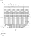
- FIG. 1 is a plan view showing a thermal print head according to a first embodiment of the present disclosure.
- FIG. 2 is a cross-sectional view taken along line II-II in FIG. 1, and shows the printer according to the first embodiment of the present disclosure.
- FIG. 3 is an enlarged plan view of essential parts of the thermal print head according to the first embodiment of the present disclosure.
- FIG. 4 is an enlarged sectional view of a main part taken along line IV-IV in FIG. 3.
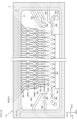
- FIG. 5 is an enlarged plan view of essential parts of the thermal print head according to the first embodiment of the present disclosure.
- FIG. 6 is an enlarged plan view of the main parts of the thermal print head according to the first embodiment of the present disclosure.
- FIG. 1 is a plan view showing a thermal print head according to a first embodiment of the present disclosure.
- FIG. 2 is a cross-sectional view taken along line II-II in FIG. 1, and shows the printer according to the first embodiment of the present disclosure.
- FIG. 3 is an enlarged plan view
- FIG. 7 is an enlarged cross-sectional view of a main part taken along line VII-VII in FIG.
- FIG. 8 is a flowchart illustrating a method for manufacturing a thermal print head according to the first embodiment of the present disclosure.
- FIG. 9 is an enlarged cross-sectional view of main parts showing a method for manufacturing a thermal print head according to the first embodiment of the present disclosure.
- FIG. 10 is an enlarged cross-sectional view of main parts showing a method of manufacturing a thermal print head according to the first embodiment of the present disclosure.
- FIG. 11 is an enlarged sectional view of a main part showing a method for manufacturing a thermal print head according to a first embodiment of the present disclosure.
- FIG. 9 is an enlarged cross-sectional view of main part taken along line VII-VII in FIG.
- FIG. 8 is a flowchart illustrating a method for manufacturing a thermal print head according to the first embodiment of the present disclosure.
- FIG. 9 is an enlarged cross-sectional view of main parts showing
- FIG. 12 is an enlarged cross-sectional view of main parts showing a method for manufacturing a thermal print head according to the first embodiment of the present disclosure.
- FIG. 13 is an enlarged plan view of main parts showing a method of manufacturing a thermal print head according to the first embodiment of the present disclosure.
- FIG. 14 is an enlarged sectional view of a main part taken along line XIV-XIV in FIG. 13.
- FIG. 15 is an enlarged plan view of main parts showing a method of manufacturing a thermal print head according to the first embodiment of the present disclosure.
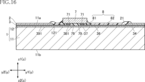
- FIG. 16 is an enlarged sectional view of a main part taken along line XVI-XVI in FIG. 15.
- FIG. 17 is an enlarged plan view of main parts showing a thermal print head according to a second embodiment of the present disclosure.
- FIG. 18 is an enlarged plan view of main parts showing a thermal print head according to a second embodiment of the present disclosure.
- FIG. 19 is an enlarged sectional view of a main part taken along line XIX-XIX in FIG. 17.
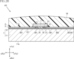
- FIG. 20 is an enlarged sectional view of main parts showing a thermal print head according to a third embodiment of the present disclosure.
- a thing A is formed on a thing B and "a thing A is formed on a thing B” mean “a thing A is formed on a thing B” unless otherwise specified.
- "something A is placed on something B” and “something A is placed on something B” mean "something A is placed on something B” unless otherwise specified.
- a certain surface A faces (one side or the other side of) the direction B is not limited to the case where the angle of the surface A with respect to the direction B is 90 degrees; Including cases where it is tilted to the opposite direction.
- First embodiment: 1 to 7 show a thermal print head A1 and a thermal printer P1 according to a first embodiment of the present disclosure.
- the thermal print head A1 includes a substrate 1, a protective layer 2, a wiring layer 3, a resistor layer 4, a plurality of drive ICs 7, a protective resin 78, a filled resin layer 8, and a heat dissipation member 9.
- the thermal print head A1 is incorporated into a thermal printer P1 that prints on a print medium C1 (see FIG. 2).
- the thermal printer P1 includes a thermal print head A1 and a platen roller B1.
- the platen roller B1 directly faces the thermal print head A1.
- the print medium C1 is sandwiched between the thermal print head A1 and the platen roller B1, and is conveyed in the sub-scanning direction y by the platen roller B1.
- Examples of such print media C1 include thermal paper for creating barcode sheets and receipts.
- a flat rubber platen may be used instead of the platen roller B1. This platen includes a portion of a cylindrical rubber having a large radius of curvature that is arch-shaped in cross-section.
- FIG. 1 is a plan view showing the thermal print head A1.
- FIG. 2 is a cross-sectional view taken along line II-II in FIG. 1, and shows the printer according to the first embodiment of the present disclosure.
- FIG. 3 is an enlarged plan view of the main parts of the thermal print head A1.
- FIG. 4 is an enlarged sectional view of a main part taken along line IV-IV in FIG. 3.
- FIG. 5 is an enlarged plan view of the main parts of the thermal print head A1.
- FIG. 6 is an enlarged plan view of the main parts of the thermal print head A1.
- FIG. 7 is an enlarged cross-sectional view of a main part taken along line VII-VII in FIG. In FIG. 1, the protective layer 2 is omitted.
- FIG. 1 is a plan view showing the thermal print head A1.
- FIG. 2 is a cross-sectional view taken along line II-II in FIG. 1, and shows the printer according to the first embodiment of the present disclosure.
- FIG. 3 is an enlarged plan view
- the protective layer 2 is omitted, and the wiring layer 3 is hatched.
- the protective resin 78 is omitted.
- the protective layer 2 and the filled resin layer 8 are hatched.
- the drive IC 7 and the filled resin layer 8 are shown with imaginary lines.
- the thickness direction of the substrate 1 is defined as the thickness direction z.
- One side in the thickness direction z may be referred to as the z1 side, and the other side may be referred to as the z2 side.
- the main scanning direction x and the sub-scanning direction y are both directions orthogonal to the thickness direction z.
- the print medium C1 is sent from the y2 side to the y1 side in the sub-scanning direction y.
- the y1 side is sometimes referred to as downstream, and the y2 side is sometimes referred to as upstream.
- the substrate 1 has a plate shape that extends long in the main scanning direction x.
- the substrate 1 is a support member that supports a protective layer 2 , a wiring layer 3 , a resistor layer 4 , and a plurality of drive ICs 7 .
- Substrate 1 has base material 11 and glaze layer 12 .
- the base material 11 includes ceramics such as AlN (aluminum nitride), Al 2 O 3 (alumina), and zirconia, and has these ceramics as its main component.
- the thickness of the base material 11 is, for example, 0.6 mm or more and 1.0 mm or less.
- the base material 11 has a rectangular shape that extends in the main scanning direction x when viewed from above.
- the base material 11 has a main surface 11a and a first back surface 11b.
- the main surface 11a and the first back surface 11b are spaced apart in the thickness direction z.
- the main surface 11a faces the z1 side in the thickness direction z.
- the first back surface 11b faces the z2 side in the thickness direction z.
- the main surface 11a is the main surface of the present disclosure, and the first back surface 11b is the back surface of the present disclosure.
- the glaze layer 12 is formed on the main surface 11a of the base material 11. Glaze layer 12 covers main surface 11a. Glaze layer 12 is made of a glass material such as amorphous glass.
- the glaze layer 12 of this example includes a bulged portion 122 and a flat portion 121. Note that the glaze layer 12 may have a configuration including the flat portion 121 and not including the bulging portion 122.
- the bulging portion 122 extends long in the main scanning direction x.
- the bulging portion 122 bulges in the thickness direction z when viewed in the main scanning direction x.
- the bulging portion 122 has an arcuate cross section (yz cross section) taken along a plane perpendicular to the main scanning direction x.
- the bulging portion 122 is provided to make it easier to press a heat generating portion (heat generating portion 41 to be described later) of the resistor layer 4 against the print medium C1.
- the bulging portion 122 is provided as a heat storage layer that accumulates heat from the heat generating portion 41.
- the bulging portion 122 has a larger dimension (maximum dimension) in the thickness direction z than the flat portion 121 .
- the flat portion 121 is formed adjacent to the bulging portion 122, and has a flat surface on the z1 side in the thickness direction z.
- the thickness of the flat portion 121 is, for example, about 2.0 ⁇ m.
- the flat portion 121 is for forming a smooth surface suitable for forming the wiring layer 3 by covering the main surface 11a of the base material 11, which is a relatively rough surface.
- the softening point of the glaze layer 12 is not limited at all.
- the softening point of the flat portion 121 and the softening point of the bulging portion 122 may be different from each other or may be the same.
- the softening point of the flat portion 121 and the bulging portion 122 is, for example, 800° C. or higher and 850° C. or lower, or approximately 680° C., for example.
- the substrate 1 of this embodiment is provided with a plurality of terminals 19.
- the plurality of terminals 19 are arranged in the main scanning direction x, for example, along the edge of the substrate 1 on the y2 side in the sub-scanning direction y.
- the wiring layer 3 constitutes a conduction path for supplying current to the resistor layer 4 .
- the wiring layer 3 is formed of a conductive material.
- the wiring layer 3 contains at least Ag (silver). Further, another part of the wiring layer 3 may contain other than Ag (silver), such as Au (gold).
- Examples of the wiring layer 3 containing Ag (silver) include those formed by printing and firing a paste containing an organic Ag compound or a paste containing Ag particles, glass frit, Pd (palladium), and a resin. .
- the portions of the wiring layer 3 shown in FIGS. 5 to 7, for example, have Ag (silver) as a main component.
- the plurality of strips 32 and the plurality of strips 35 in contact with the resistor layer 4 in the wiring layer 3 may be mainly composed of, for example, Au (gold).
- the thickness of the wiring layer 3 is not limited at all, and is, for example, 1 ⁇ m or more and 10 ⁇ m or less.
- the wiring layer 3 is formed on the glaze layer 12 of the substrate 1.
- the wiring layer 3 has a common electrode 31 and a plurality of individual electrodes 34, as shown in FIGS. 3 and 4. Note that the shape and arrangement of each part of the wiring layer 3 are not limited to the examples shown in FIGS. 3 and 4, and can be configured in various ways.
- the common electrode 31 has a plurality of strip portions 32 and connecting portions 33.
- the connecting portion 33 is disposed near the edge of the substrate 1 on the y1 side in the sub-scanning direction y, and has a band shape extending in the main scanning direction x.
- the plurality of strips 32 each extend from the connecting portion 33 toward the y2 side in the sub-scanning direction y, and are arranged at equal pitches in the main-scanning direction x.
- the auxiliary layer 331 is laminated on the connecting portion 33 in order to reduce the resistance value of the connecting portion 33, but the auxiliary layer 331 does not need to be laminated.
- the auxiliary layer 331 is formed, for example, by printing and baking a paste containing an organic Ag (silver) compound or a paste containing Ag (silver) particles, glass frit, Pd (palladium), and a resin.
- the plurality of individual electrodes 34 are for partially supplying current to the resistor layer 4. Each individual electrode 34 has opposite polarity to the common electrode 31. Each individual electrode 34 extends from the resistor layer 4 toward the drive IC 7. The plurality of individual electrodes 34 are arranged in the main scanning direction x.
- the specific structure of the resistor layer 4 is not limited at all, and each of the plurality of individual electrodes 34 has a strip portion 35, a connecting portion 36, and a first pad portion 37.
- the strip portion 35 extends in the sub-scanning direction y and is strip-shaped when viewed in the thickness direction z.
- Each strip 35 is located between two adjacent strips 32 of the common electrode 31 .
- the distance between the adjacent strip portions 35 of the individual electrodes 34 and the strip portions 32 of the common electrode 31 is, for example, 50 ⁇ m or less.
- the plurality of first pad portions 37 are formed at the ends of the individual electrodes 34 on the y2 side in the sub-scanning direction y.
- the shape of the first pad portion 37 is not limited in any way, and in the illustrated example, it is circular.
- the plurality of first pad sections 37 include a plurality of first pad sections 37A and a plurality of first pad sections 37B.
- the plurality of first pad sections 37A are arranged at equal pitches along the main scanning direction x.
- the first pad portions 37B are arranged on the y2 side of the first pad portion 37A in the sub-scanning direction y, and are arranged at equal pitches along the main-scanning direction x. That is, the plurality of first pad sections 37 are arranged in a staggered manner.
- the first pad portion 37B is connected to a straight portion 361 sandwiched between two adjacent first pad portions 37A.
- the connecting portion 36 is a portion extending from the strip portion 35 toward the plurality of first pad portions 37, as shown in FIGS. 3, 5, and 6.
- the connecting portion 36 includes a straight portion 361, an inclined portion 362, an intermediate portion 363, and a second pad portion 364.
- the straight portion 361 has one end connected to the first pad portion 37 and extends along the sub-scanning direction y.
- the inclined portion 362 is connected to the end of the strip portion 35 on the y2 side in the sub-scanning direction y, and is inclined with respect to the sub-scanning direction y.
- the intermediate portion 363 is interposed between the straight portion 361 and the inclined portion 362.
- the shape of the intermediate portion 363 is not limited at all, and in the illustrated example, it is a bent band-shaped portion.
- the second pad section 364 is interposed between the first pad section 37 and the heat generating section 41, and is formed integrally with the intermediate section 363 in the illustrated example.
- the size and shape of the second pad portion 364 are not limited in any way, and in this embodiment, it is larger than the first pad portion 37 .
- the second pad portion 364 has a substantially pentagonal shape.
- the second pad portions 364 of the connecting portions 36 of the plurality of individual electrodes 34 constitute a plurality of second pad portions 364.
- the arrangement of the plurality of second pad sections 364 is not limited at all.
- the plurality of second pad sections 364 include a plurality of second pad sections 364A and a plurality of second pad sections 364B.
- the plurality of second pad sections 364A are arranged at equal pitches along the main scanning direction x.
- the plurality of second pad sections 364B are arranged at equal pitches along the main scanning direction x on the y2 side of the sub-scanning direction y with respect to the plurality of second pad sections 364A. That is, the plurality of second pad sections 364 are arranged in a staggered manner.
- An intermediate portion 363 integrally formed with the second pad portion 364B is arranged between the adjacent second pad portions 364A.
- An intermediate portion 363 integrally formed with the second pad portion 364A is arranged between the adjacent second pad portions 364B.
- the second pad section 364A and the second pad section 364B are symmetrical about the axis of symmetry extending in the main scanning direction x.
- the plurality of pad sections include a plurality of pad sections 381 and a plurality of pad sections 382 in addition to the plurality of first pad sections 37 described above.
- the wiring layer 3 includes a wiring part 391 and a plurality of wiring parts 392.
- the plurality of pad sections 381 are arranged at equal pitches along the main scanning direction x.
- the plurality of pad sections 381 are arranged on the y2 side in the sub-scanning direction y with respect to the plurality of first pad sections 37.
- the plurality of pad sections 381 are connected to a wiring section 391.
- the wiring section 391 is arranged on the y2 side in the sub-scanning direction y with respect to the plurality of pad sections 381, and has a rectangular shape in the illustrated example.
- the wiring section 391 is, for example, a part of a power supply line for realizing printing by the thermal print head A1.
- the plurality of pad sections 382 are arranged on both sides of the plurality of first pad sections 37 and the plurality of first pad sections 37 in the main scanning direction x.
- the plurality of pad sections 382 are arranged in the main scanning direction x together with the plurality of first pad sections 37A, and the plurality of pad sections 382 are arranged in the main scanning direction x together with the plurality of pad sections 381. and, including.
- the plurality of pad sections 382 include those connected to the plurality of wiring sections 392.
- the resistor layer 4 is formed using a material having higher resistivity than the material constituting the wiring layer 3.
- the resistor layer 4 contains, for example, ruthenium oxide.
- the resistor layer 4 is formed on the bulge 122, as shown in FIGS. 3 and 4.
- the shape of the resistor layer 4 when viewed in the thickness direction z is not limited at all, and in this embodiment, as shown in FIGS. 1 and 3, it is a band shape extending in the main scanning direction x.
- the resistor layer 4 intersects each strip 32 (common electrode 31) and each strip 35 (individual electrode 34).
- the resistor layer 4 is laminated on the z1 side of the plurality of strips 32 and the plurality of strips 35 in the thickness direction z.
- a portion of the resistor layer 4 sandwiched between each strip portion 32 and each strip portion 35 serves as a heat generating portion 41 .
- the plurality of heat generating parts 41 generate heat by being partially energized by the wiring layer 3 .
- Print dots are formed by the heat generated by each heat generating section 41.
- the plurality of heat generating parts 41 are arranged in the main scanning direction x. The greater the number of heat generating parts 41 arranged in the main scanning direction x in the unit length (for example, 1 mm) of the substrate 1 in the main scanning direction x, the greater the dot density of the thermal print head A1.
- the thickness of the resistor layer 4 is, for example, 3 ⁇ m or more and 6 ⁇ m or less.
- the resistor layer 4 is formed on the top of the bulge 122, but may not be formed on the top of the bulge 122.
- the protective layer 2 is for protecting the wiring layer 3, the resistor layer 4, and the like.
- the protective layer 2 may have a single layer structure, or may have a structure in which a plurality of layers are laminated.
- the material of the protective layer 2 is not limited at all.
- An example of the protective layer 2 includes, for example, amorphous glass as a main component.
- a first layer made of amorphous glass and a second layer made of SiAlON, for example, may be laminated.
- SiAlON is a silicon nitride-based engineering ceramic made by synthesizing Si 3 N 4 (silicon nitride) with Al 2 O 3 (alumina) and SiO 2 (silica).
- the second layer is formed by sputtering, for example.
- the second layer may be made of SiC (silicon carbide) instead of SiAlON.
- the protective layer 2 has an opening 21.
- the opening 21 is constituted by a through hole that penetrates the protective layer 2 in the thickness direction z.
- the shape, size, and arrangement of the opening 21 are not limited at all, and are appropriately set depending on the configuration of the plurality of drive ICs 7, the wiring layer 3, and the like.
- the opening 21 is formed in a substantially rectangular shape.
- the opening 21 exposes the plurality of first pad parts 37. That is, the plurality of first pad portions 37 are exposed from the protective layer 2 through the opening 21 and are included in the opening 21 when viewed in the thickness direction z. Furthermore, in this embodiment, the plurality of second pad portions 364 are enclosed within the opening 21 when viewed in the thickness direction z. Furthermore, the plurality of pad portions 381 and the plurality of pad portions 382 are enclosed within the opening 21 when viewed in the thickness direction z.
- the edge of the opening 21 on the y1 side in the sub-scanning direction y intersects with the plurality of individual electrodes 34.
- the edge of the opening 21 on the y1 side in the sub-scanning direction y intersects with the inclined portion 362 or the intermediate portion 363.
- the edge of the opening 21 on the y2 side in the sub-scanning direction y intersects with the wiring portion 391.
- the edges of the opening 21 on both sides in the main scanning direction x intersect with the plurality of wiring portions 392 .
- a plurality of drive ICs 7 are mounted on the substrate 1.
- the plurality of drive ICs 7 are for individually energizing the plurality of heat generating parts 41.
- the drive IC 7 has a plurality of electrodes 71. As shown in FIG. 7, the plurality of electrodes 71 are conductively bonded onto the wiring layer 3 by a bonding layer 79 through the opening 21. Bonding layer 79 is, for example, solder. Thereby, the plurality of drive ICs 7 are electrically connected to the wiring layer 3 and the resistor layer 4.
- the plurality of electrodes 71 are electrically connected to the plurality of first pad sections 37, the plurality of pad sections 381, and the plurality of pad sections 382 through the opening 21 via the bonding layer 79.
- the arrangement of the drive IC 7 is not limited at all, and in this embodiment, the drive IC 7 is entirely enclosed in the opening 21 when viewed in the thickness direction z.
- the power supply control to the plurality of heat generating parts 41 by the plurality of drive ICs 7 follows, for example, a command signal input from the outside of the thermal print head A1 via the plurality of terminals 19.
- the plurality of drive ICs 7 are provided as appropriate depending on the number of the plurality of heat generating parts 41.
- the filled resin layer 8 includes a portion interposed between the substrate 1 (principal surface 11a) and the drive IC 7, and in this embodiment, the filled resin layer 8 includes the flat portion 121 of the glaze layer 12 and the wiring layer 3. This is to fill the gap between the drive IC 7 and the drive IC 7. Furthermore, the filled resin layer 8 covers all of the openings 21. As shown in FIGS. 5 and 6, in this embodiment, the filled resin layer 8 extends from the drive IC 7 when viewed in the thickness direction z, and reaches the edge of the opening 21.
- the filled resin layer 8 is, for example, what is called an underfill agent, and is formed by curing a highly permeable insulating liquid (or paste, etc.).
- the material of the filled resin layer 8 is not limited at all, and conventionally known resins and the like can be used as appropriate.
- the filled resin layer 8 is in contact with a part of the side surface of the drive IC 7. Further, as shown in FIGS. 5 to 7, the filled resin layer 8 has a portion located above the protective layer 2 (a portion covering a part of the protective layer 2).
- the protective resin 78 covers the plurality of drive ICs 7, the filled resin layer 8, and a portion of the protective layer 2.
- the protective resin 78 is made of, for example, an insulating resin and is, for example, black in color. Further, the protective resin 78 may have a structure in which a plurality of layers made of a plurality of types of materials (resin, glass, etc.) are laminated. Further, in FIG. 2, the cross-sectional shape of the protective resin 78 is a shape that gently bulges toward the z1 side in the thickness direction z, but is not limited to this, and can be set to various shapes. Note that the protective resin 78 may be configured to partially cover the filled resin layer 8.
- the heat dissipation member 9 supports the substrate 1, as shown in FIGS. 1 and 2.
- the heat radiating member 9 is for radiating a part of the heat generated by the plurality of heat generating parts 41 to the outside via the substrate 1.
- the heat dissipation member 9 is a block-shaped member made of metal such as Al (aluminum), for example.
- the heat dissipation member 9 has a support surface 91, as shown in FIG.
- the support surface 91 faces the z1 side in the thickness direction z.
- the first back surface 11b of the base material 11 is joined to the support surface 91.
- thermal print head A1 Next, a method for manufacturing the thermal print head A1 will be described below with reference to FIGS. 8 to 16.
- FIG. 8 is a flowchart showing a method for manufacturing the thermal print head A1.
- the manufacturing method of the thermal print head A1 of this embodiment includes a step of preparing a substrate 1, a step of forming a wiring layer 3 and a resistor layer 4, a step of forming the wiring layer 3, and a step of conductively bonding the driving IC 7 to the wiring layer 3. and a step of forming a filled resin layer 8.
- a substrate 1 is prepared.
- the substrate 1 is obtained by forming the glaze layer 12 on the main surface 11a of the base material 11.
- a wiring layer 3 and a resistor layer 4 are formed.
- the wiring layer 3 is formed by, for example, printing a paste containing an organic Ag compound or a paste containing Ag particles, glass frit, Pd (palladium), and a resin on the glaze layer 12, and then firing this. As a result, a conductive film containing Ag (silver) is obtained.
- the wiring layer 3 is obtained by appropriately patterning this conductive film.
- a paste containing, for example, ruthenium oxide is printed along the main scanning direction x so as to cross the plurality of strips 32 and the plurality of strips 35, and is fired. Thereby, the resistor layer 4 is obtained.
- a protective layer 2 is formed.
- the protective layer 2 can be formed, for example, by printing a glass paste and firing it.
- the openings 21 are provided, for example, by not printing glass paste in areas where the openings 21 are to be formed when printing glass paste.
- the plurality of electrodes 71 of the drive IC 7 are electrically connected to the wiring layer 3 through the bonding layer 79.
- the plurality of electrodes 71 are electrically connected to the plurality of first pad sections 37 , the plurality of pad sections 381 , and the plurality of pad sections 381 .
- the drive IC 7 is enclosed in the opening 21 when viewed in the thickness direction z.
- a filled resin layer 8 is formed.
- the first portion 81 is formed.
- An underfill agent or the like is filled into the gap between the glaze layer 12 (principal surface 11a), the wiring layer 3, and the drive IC 7 using a dispenser.
- this underfill agent is attached to a part of the side surface of the drive IC 7.
- this underfill agent remains directly below or near the drive IC 7 when viewed in the thickness direction z, and is spaced apart from the edge of the opening 21 .
- the first portion 81 is formed by appropriately curing the underfill agent.
- the second portion 82 is formed.
- An underfill agent or the like is applied to the region between the first portion 81 and the edge of the opening 21 when viewed in the thickness direction z. That is, the coating is applied to a portion of the opening 21 that is not covered by the first portion 81 .
- the second portion 82 covers, for example, the plurality of second pad portions 364.
- an underfill agent is applied to a portion of the protective layer 2.
- the second portion 82 is formed by appropriately curing the underfill agent, and as a result, the filled resin layer 8 consisting of the first portion 81 and the second portion 82 is formed.
- the filled resin layer 8 may have a structure in which the first part 81 and the second part 82 are distinguishable from each other, or may have a structure in which the first part 81 and the second part 82 are integrated and cannot be distinguished from each other. good. For example, if the first part 81 and the second part 82 are formed with underfill agents of different materials, or if the first part 81 and the second part 82 are cured at different timings. In such cases, the filled resin layer 8 may have a structure in which the first portion 81 and the second portion 82 are distinguishable from each other.
- the thermal print head A1 is obtained by forming the protective resin 78, attaching the substrate 1 to the heat radiating member 9, etc.
- the drive IC 7 is electrically connected to the plurality of first pad portions 37 through the opening 21. All of the openings 21 are closed by the filled resin layer 8. Thereby, it is possible to suppress unintended components contained in the outside air or the like in the operating environment of the thermal print head A1 from corroding the wiring layer 3. Therefore, the occurrence of ion migration in the wiring layer 3 can be suppressed.
- the first part 81 shown in FIGS. 13 and 14 is formed, and the second part 82 shown in FIGS. 15 and 16 is formed.
- the first portion 81 it is possible to sufficiently fill the gap between the substrate 1, the wiring layer 3, and the drive IC 7 with an underfill agent or the like.
- the second portion 82 it is possible to more reliably cover the region of the opening 21 that largely extends from the drive IC 7, that is, the region that is not covered by the first portion 81. Therefore, even if the opening 21 becomes larger, the occurrence of ion migration in the wiring layer 3 can be suppressed.
- a plurality of second pad portions 364 are included in the opening 21.
- the resistance value can be made appropriate by performing laser trimming, for example.
- Second embodiment: 17 to 19 show a thermal print head according to a second embodiment of the present disclosure.
- the thermal print head A2 of this embodiment differs from the embodiments described above mainly in the configurations of the protective layer 2, the wiring layer 3, and the filled resin layer 8.
- each of the connecting portions 36 of the plurality of individual electrodes 34 of the wiring layer 3 does not have the above-mentioned intermediate portion 363 and second pad portion 364.
- the straight portion 361 and the inclined portion 362 are connected.
- the edge of the opening 21 on the y1 side in the sub-scanning direction y intersects with the inclined portion 362 of the connecting portion 36 of the plurality of individual electrodes 34.
- the distance between the edge of the opening 21 on the y1 side in the sub-scanning direction y and the drive IC 7 is smaller than the distance in the thermal print head A1, for example.
- the occurrence of ion migration in the wiring layer 3 can be suppressed.
- the connecting portion 36 does not include the intermediate portion 363 and the second pad portion 364, the opening portion 21 can be reduced. This makes it possible to reduce the area of the portion of the wiring layer 3 exposed from the opening 21, which is preferable for suppressing the occurrence of ion migration in the wiring layer 3.
- the resistance values of the plurality of heat generating parts 41 described above may be measured using, for example, the plurality of first pad parts 37.
- FIG. 20 shows a thermal print head according to a third embodiment of the present disclosure.
- the thermal print head A3 of this embodiment differs from the embodiments described above mainly in the configurations of the protective layer 2, drive IC 7, and filled resin layer 8.
- At least a portion of the edge of the opening 21 overlaps the drive IC 7 when viewed in the thickness direction z. In the illustrated example, all edges of the opening 21 overlap the drive IC 7 when viewed in the thickness direction z.
- the filled resin layer 8 covers all of the openings 21.
- the filled resin layer 8 may be configured only by the first portion 81 described above, for example.
- the opening 21 may be opened so as to appropriately connect the drive IC 7 and the wiring layer 3 to each other.
- the opening 21 is not limited to a configuration that encloses all of the drive IC 7, but may have a configuration that only includes a part of the drive IC 7.
- thermal print head, thermal printer, and method for manufacturing a thermal print head according to the present disclosure are not limited to the embodiments described above.
- the specific configurations of the thermal print head, thermal printer, and method of manufacturing the thermal print head according to the present disclosure can be modified in various designs.
- the present disclosure includes the embodiments described in the appendix below.
- a base material having a main surface and a back surface facing oppositely to each other in the thickness direction; a wiring layer and a resistor layer supported on the main surface; a protective layer that covers a portion of the wiring layer and at least a portion of the resistor layer; a drive IC that controls energization to the resistor layer and is disposed on the main surface; a filled resin layer having a portion interposed between the main surface and the drive IC,
- the wiring layer contains Ag and has a plurality of pad portions,
- the drive IC has a plurality of electrodes,
- the protective layer has an opening that exposes the plurality of pad parts, The plurality of electrodes are electrically connected to the plurality of pad portions through the opening,
- the filled resin layer covers all of the openings of the thermal print head.
- the thermal print head according to appendix 1 further comprising a protective resin that covers the drive IC and at least a portion of the filled resin layer when viewed in the thickness direction.
- Appendix 3. The thermal print head according to appendix 2, wherein the protective resin covers all of the filled resin layer when viewed in the thickness direction.
- Appendix 4. The thermal print head according to any one of Supplementary Notes 1 to 3, wherein all of the drive ICs are included in the opening when viewed in the thickness direction. Appendix 5.
- the thermal print head according to appendix 5 wherein the wiring layer includes a plurality of individual wirings individually connected to the plurality of heat generating parts. Appendix 7. Each of the individual wirings has a first pad portion, The thermal print head according to appendix 6, wherein the plurality of pad portions include the first pad portions of the plurality of individual wirings. Appendix 8. The thermal print head according to appendix 7, wherein the first pad portions of the plurality of individual wirings are arranged along the main scanning direction. Appendix 9. According to appendix 8, each of the individual wirings has a straight part connected to the first pad part and extending in the sub-scanning direction, and an inclined part connected to the straight part and inclined with respect to the sub-scanning direction. thermal print head. Appendix 10.
- Each of the individual wirings has a second pad portion interposed between each of the heat generating portions and the first pad portion,
- Appendix 12 The thermal print head according to appendix 11, wherein the second pad portion is larger than the first pad portion.
- Appendix 13 The thermal print head according to appendix 11 or 12, wherein the second pad portions of the plurality of individual wirings are arranged in a staggered manner along the main scanning direction.
- Appendix 16 The thermal print head according to any one of appendices 1 to 15, further comprising a glaze layer interposed between the base material, the resistor layer, and the wiring layer.
- Appendix 17. A thermal printer comprising the thermal print head described in Appendix 1. Appendix 18.
- the wiring layer contains Ag and has a plurality of pad portions
- the drive IC has a plurality of electrodes
- the protective layer has an opening that exposes the plurality of pad parts, In the step of electrically bonding the driving IC to the wiring layer, electrically bonding the plurality of electrodes to the plurality of pad portions through the opening,
- the step of forming the filled resin layer includes a step of forming a first part interposed between the main surface and the drive IC and spaced apart from an edge of the opening, and a step of forming the first part and the opening.
Abstract
This thermal printhead comprises a substrate, a wiring layer and a resistor layer, a protective layer, a driver IC, and a filling resin layer having a portion interposed between a main surface and the driver IC, wherein the wiring layer comprises Ag and has a plurality of first pads, the driver IC has a plurality of electrodes, the protective layer has openings where the plurality of electrodes are exposed, the plurality of electrodes are electrically connected to the plurality of first pads through the openings, and the filling resin layer fills all of the openings.
Description
本開示は、サーマルプリントヘッド、サーマルプリンタおよびサーマルプリントヘッドの製造方法に関する。
The present disclosure relates to a thermal print head, a thermal printer, and a method for manufacturing a thermal print head.
従来、感熱紙や感熱インクリボンに対して熱を付与することにより印刷を行うデバイスとして、サーマルプリントヘッドが用いられている。たとえば、特許文献1には、従来のサーマルプリントヘッドが開示されている。特許文献1に記載のサーマルプリントヘッドは、基板、配線層、抵抗体層、保護層、駆動ICおよび封止樹脂を備える。抵抗体層は、配線層を介して駆動ICと導通している。同文献では、配線層は、Agを含む。
Conventionally, a thermal print head has been used as a device that prints by applying heat to thermal paper or thermal ink ribbon. For example, Patent Document 1 discloses a conventional thermal print head. The thermal print head described in Patent Document 1 includes a substrate, a wiring layer, a resistor layer, a protective layer, a driving IC, and a sealing resin. The resistor layer is electrically connected to the drive IC via the wiring layer. In this document, the wiring layer contains Ag.
Agを含む配線層に電圧が印加されると、イオンマイグレーションが発生する場合がある。イオンマイグレーションによって配線層の一部同士が接触すると、電気的なショートが生じるおそれがある。
When a voltage is applied to a wiring layer containing Ag, ion migration may occur. If parts of the wiring layers come into contact with each other due to ion migration, an electrical short may occur.
本開示は、従来より改良が施されたサーマルプリントヘッド、サーマルプリンタおよびサーマルプリントヘッドの製造方法を提供することを一の課題とする。特に本開示は、上記した事情に鑑み、配線層におけるイオンマイグレーションの発生を抑制することが可能なサーマルプリントヘッド、サーマルプリンタおよびサーマルプリントヘッドの製造方法を提供することをその一の課題とする。
An object of the present disclosure is to provide a thermal print head, a thermal printer, and a method for manufacturing a thermal print head that are improved from the conventional ones. In particular, in view of the above-mentioned circumstances, one object of the present disclosure is to provide a thermal print head, a thermal printer, and a method for manufacturing a thermal print head that can suppress the occurrence of ion migration in a wiring layer.
本開示の第1の側面によって提供されるサーマルプリントヘッドは、厚さ方向において互いに反対側を向く主面および裏面を有する基材と、前記主面に支持された配線層および抵抗体層と、前記配線層の一部および前記抵抗体層の少なくとも一部ずつを覆う保護層と、前記抵抗体層への通電を制御し、且つ前記主面に配置された駆動ICと、前記主面と前記駆動ICとの間に介在する部分を有する充填樹脂層と、を備える。前記配線層は、Agを含み、且つ複数のパッド部を有する。前記駆動ICは、複数の電極を有する。前記保護層は、前記複数のパッド部を露出させる開口部を有する。前記複数の電極は、前記開口部を通じて前記複数のパッド部に導通接合されている。前記充填樹脂層は、前記開口部のすべてを塞いでいる。
A thermal print head provided by a first aspect of the present disclosure includes: a base material having a main surface and a back surface facing opposite to each other in the thickness direction; a wiring layer and a resistor layer supported on the main surface; a protective layer that covers at least a portion of the wiring layer and at least a portion of the resistor layer; a drive IC that controls energization to the resistor layer and is disposed on the main surface; and a filled resin layer having a portion interposed between the drive IC and the drive IC. The wiring layer contains Ag and has a plurality of pad portions. The drive IC has a plurality of electrodes. The protective layer has an opening that exposes the plurality of pad sections. The plurality of electrodes are electrically connected to the plurality of pad portions through the opening. The filled resin layer covers all of the openings.
本開示の第2の側面によって提供されるサーマルプリンタは、本開示の第1の側面によって提供されるサーマルプリントヘッドを備える。
The thermal printer provided by the second aspect of the present disclosure includes the thermal print head provided by the first aspect of the present disclosure.
本開示の第3の側面によって提供されるサーマルプリントヘッドの製造方法は、厚さ方向において互いに反対側を向く主面および裏面を有する基材を用意する工程と、前記主面に支持された配線層および抵抗体層を形成する工程と、前記配線層の一部および前記抵抗体層の少なくとも一部ずつを覆う保護層を形成する工程と、前記配線層に駆動ICを導通接合する工程と、前記主面と前記駆動ICとの間に介在する部分を有する充填樹脂層を形成する工程と、を備える。前記配線層は、Agを含み、且つ複数のパッド部を有する。前記駆動ICは、複数の電極を有する。前記保護層は、前記複数のパッド部を露出させる開口部を有する。前記配線層に前記駆動ICを導通接合する工程においては、前記開口部を通じて前記複数の電極を前記複数のパッド部に導通接合する。前記充填樹脂層を形成する工程は、前記主面と前記駆動ICとの間に介在し且つ前記開口部の端縁から離隔した第1部を形成する工程と、前記第1部と前記開口部の端縁との間の領域を塞ぐ第2部を形成する工程と、を含む。
A method for manufacturing a thermal print head provided by a third aspect of the present disclosure includes the steps of: preparing a base material having a main surface and a back surface facing oppositely to each other in the thickness direction; and wiring supported on the main surface. a step of forming a protective layer covering a portion of the wiring layer and at least a portion of the resistor layer; and a step of conductively bonding a driving IC to the wiring layer; forming a filled resin layer having a portion interposed between the main surface and the drive IC. The wiring layer contains Ag and has a plurality of pad portions. The drive IC has a plurality of electrodes. The protective layer has an opening that exposes the plurality of pad parts. In the step of electrically bonding the driving IC to the wiring layer, the plurality of electrodes are electrically bonded to the plurality of pad portions through the opening. The step of forming the filled resin layer includes a step of forming a first part interposed between the main surface and the drive IC and spaced apart from an edge of the opening, and a step of forming the first part and the opening. forming a second portion that closes a region between the edge of the substrate and the edge of the substrate.
上記構成によれば、配線層におけるイオンマイグレーションの発生を抑制することが可能である。
According to the above configuration, it is possible to suppress the occurrence of ion migration in the wiring layer.
本開示のその他の特徴および利点は、添付図面を参照して以下に行う詳細な説明によって、より明らかとなろう。
Other features and advantages of the present disclosure will become more apparent from the detailed description given below with reference to the accompanying drawings.
以下、本開示の好ましい実施の形態につき、図面を参照して具体的に説明する。
Hereinafter, preferred embodiments of the present disclosure will be specifically described with reference to the drawings.
本開示における「第1」、「第2」、「第3」等の用語は、単に識別のために用いたものであり、それらの対象物に順列を付することを意図していない。
Terms such as "first," "second," and "third" in the present disclosure are used merely for identification purposes and are not intended to impose any order on these objects.
本開示において、「ある物Aがある物Bに形成されている」および「ある物Aがある物B上に形成されている」とは、特段の断りのない限り、「ある物Aがある物Bに直接形成されていること」、および、「ある物Aとある物Bとの間に他の物を介在させつつ、ある物Aがある物Bに形成されていること」を含む。同様に、「ある物Aがある物Bに配置されている」および「ある物Aがある物B上に配置されている」とは、特段の断りのない限り、「ある物Aがある物Bに直接配置されていること」、および、「ある物Aとある物Bとの間に他の物を介在させつつ、ある物Aがある物Bに配置されていること」を含む。同様に、「ある物Aがある物B上に位置している」とは、特段の断りのない限り、「ある物Aがある物Bに接して、ある物Aがある物B上に位置していること」、および、「ある物Aとある物Bとの間に他の物が介在しつつ、ある物Aがある物B上に位置していること」を含む。また、「ある物Aがある物Bにある方向に見て重なる」とは、特段の断りのない限り、「ある物Aがある物Bのすべてに重なること」、および、「ある物Aがある物Bの一部に重なること」を含む。また、本開示において「ある面Aが方向B(の一方側または他方側)を向く」とは、面Aの方向Bに対する角度が90°である場合に限定されず、面Aが方向Bに対して傾いている場合を含む。
In this disclosure, "a thing A is formed on a thing B" and "a thing A is formed on a thing B" mean "a thing A is formed on a thing B" unless otherwise specified. "It is formed directly on object B," and "It is formed on object B, with another object interposed between object A and object B." Similarly, "something A is placed on something B" and "something A is placed on something B" mean "something A is placed on something B" unless otherwise specified. This includes ``directly placed on object B'' and ``placed on object B with another object interposed between object A and object B.'' Similarly, "a certain object A is located on a certain object B" means, unless otherwise specified, "a certain object A is in contact with a certain object B, and a certain object A is located on a certain object B." ``The fact that a certain thing A is located on a certain thing B while another thing is interposed between the certain thing A and the certain thing B.'' In addition, "a certain object A overlaps a certain object B when viewed in a certain direction" means, unless otherwise specified, "a certain object A overlaps all of a certain object B" and "a certain object A overlaps with a certain object B". This includes "overlapping a part of something B." Furthermore, in the present disclosure, "a certain surface A faces (one side or the other side of) the direction B" is not limited to the case where the angle of the surface A with respect to the direction B is 90 degrees; Including cases where it is tilted to the opposite direction.
第1実施形態:
図1~図7は、本開示の第1実施形態に係るサーマルプリントヘッドA1およびサーマルプリンタP1を示している。サーマルプリントヘッドA1は、基板1、保護層2、配線層3、抵抗体層4、複数の駆動IC7、保護樹脂78、充填樹脂層8および放熱部材9を備える。サーマルプリントヘッドA1は、印刷媒体C1(図2参照)に印字を施すサーマルプリンタP1に組み込まれるものである。 First embodiment:
1 to 7 show a thermal print head A1 and a thermal printer P1 according to a first embodiment of the present disclosure. The thermal print head A1 includes asubstrate 1, a protective layer 2, a wiring layer 3, a resistor layer 4, a plurality of drive ICs 7, a protective resin 78, a filled resin layer 8, and a heat dissipation member 9. The thermal print head A1 is incorporated into a thermal printer P1 that prints on a print medium C1 (see FIG. 2).
図1~図7は、本開示の第1実施形態に係るサーマルプリントヘッドA1およびサーマルプリンタP1を示している。サーマルプリントヘッドA1は、基板1、保護層2、配線層3、抵抗体層4、複数の駆動IC7、保護樹脂78、充填樹脂層8および放熱部材9を備える。サーマルプリントヘッドA1は、印刷媒体C1(図2参照)に印字を施すサーマルプリンタP1に組み込まれるものである。 First embodiment:
1 to 7 show a thermal print head A1 and a thermal printer P1 according to a first embodiment of the present disclosure. The thermal print head A1 includes a
サーマルプリンタP1は、サーマルプリントヘッドA1およびプラテンローラB1を備える。プラテンローラB1は、サーマルプリントヘッドA1に正対する。印刷媒体C1は、サーマルプリントヘッドA1とプラテンローラB1との間に挟まれ、このプラテンローラB1によって、副走査方向yに搬送される。このような印刷媒体C1としては、たとえばバーコードシートやレシートを作成するための感熱紙が挙げられる。プラテンローラB1に代えて、平坦なゴムからなるプラテンを使用してもよい。このプラテンは、大きな曲率半径を有する円柱状のゴムにおける、断面視において弓形状の一部分を含む。
The thermal printer P1 includes a thermal print head A1 and a platen roller B1. The platen roller B1 directly faces the thermal print head A1. The print medium C1 is sandwiched between the thermal print head A1 and the platen roller B1, and is conveyed in the sub-scanning direction y by the platen roller B1. Examples of such print media C1 include thermal paper for creating barcode sheets and receipts. A flat rubber platen may be used instead of the platen roller B1. This platen includes a portion of a cylindrical rubber having a large radius of curvature that is arch-shaped in cross-section.
図1は、サーマルプリントヘッドA1を示す平面図である。図2は、図1のII-II線に沿う断面図であり、本開示の第1実施形態に係るプリンタを示す。図3は、サーマルプリントヘッドA1を示す要部拡大平面図である。図4は、図3のIV-IV線に沿う要部拡大断面図である。図5は、サーマルプリントヘッドA1を示す要部拡大平面図である。図6は、サーマルプリントヘッドA1を示す要部拡大平面図である。図7は、図5のVII-VII線に沿う要部拡大断面図である。図1においては、保護層2を省略している。図3においては、保護層2を省略しており、配線層3にハッチングを付している。図5および図6においては、保護樹脂78を省略している。図5においては、保護層2および充填樹脂層8にハッチングを付している。また、図6においては、駆動IC7および充填樹脂層8を想像線で示している。
FIG. 1 is a plan view showing the thermal print head A1. FIG. 2 is a cross-sectional view taken along line II-II in FIG. 1, and shows the printer according to the first embodiment of the present disclosure. FIG. 3 is an enlarged plan view of the main parts of the thermal print head A1. FIG. 4 is an enlarged sectional view of a main part taken along line IV-IV in FIG. 3. FIG. 5 is an enlarged plan view of the main parts of the thermal print head A1. FIG. 6 is an enlarged plan view of the main parts of the thermal print head A1. FIG. 7 is an enlarged cross-sectional view of a main part taken along line VII-VII in FIG. In FIG. 1, the protective layer 2 is omitted. In FIG. 3, the protective layer 2 is omitted, and the wiring layer 3 is hatched. In FIGS. 5 and 6, the protective resin 78 is omitted. In FIG. 5, the protective layer 2 and the filled resin layer 8 are hatched. Further, in FIG. 6, the drive IC 7 and the filled resin layer 8 are shown with imaginary lines.
これらの図において、基板1(後述の基材11)の厚さ方向を厚さ方向zとしている。厚さ方向zの一方側をz1側、他方側をz2側と称する場合がある。主走査方向xおよび副走査方向yは、いずれも厚さ方向zと直交する方向である。印刷時において、印刷媒体C1は、副走査方向yのy2側からy1側に送られる。副走査方向yにおいて、y1側を下流、y2側を上流と称する場合がある。
In these figures, the thickness direction of the substrate 1 (substrate 11 described below) is defined as the thickness direction z. One side in the thickness direction z may be referred to as the z1 side, and the other side may be referred to as the z2 side. The main scanning direction x and the sub-scanning direction y are both directions orthogonal to the thickness direction z. During printing, the print medium C1 is sent from the y2 side to the y1 side in the sub-scanning direction y. In the sub-scanning direction y, the y1 side is sometimes referred to as downstream, and the y2 side is sometimes referred to as upstream.
(基板1)
基板1は、図1に示すように、主走査方向xに長く延びる板状である。基板1は、保護層2、配線層3、抵抗体層4、および、複数の駆動IC7を支持する支持部材である。基板1は、基材11およびグレーズ層12を有する。 (Substrate 1)
As shown in FIG. 1, thesubstrate 1 has a plate shape that extends long in the main scanning direction x. The substrate 1 is a support member that supports a protective layer 2 , a wiring layer 3 , a resistor layer 4 , and a plurality of drive ICs 7 . Substrate 1 has base material 11 and glaze layer 12 .
基板1は、図1に示すように、主走査方向xに長く延びる板状である。基板1は、保護層2、配線層3、抵抗体層4、および、複数の駆動IC7を支持する支持部材である。基板1は、基材11およびグレーズ層12を有する。 (Substrate 1)
As shown in FIG. 1, the
基材11は、たとえばAlN(窒化アルミニウム)、Al2O3(アルミナ)、ジルコニアなどのセラミックを含み、たとえばこれらのセラミックスを主成分とする。基材11は、たとえばその厚さが0.6mm以上1.0mm以下である。基材11は、図1に示すように、平面視において、主走査方向xに長く延びる矩形状とされている。基材11は、主面11aおよび第1裏面11bを有する。主面11aと第1裏面11bとは、厚さ方向zに離間する。主面11aは、厚さ方向zのz1側を向く。第1裏面11bは、厚さ方向zのz2側を向く。主面11aは、本開示の主面であり、第1裏面11bは、本開示の裏面である。
The base material 11 includes ceramics such as AlN (aluminum nitride), Al 2 O 3 (alumina), and zirconia, and has these ceramics as its main component. The thickness of the base material 11 is, for example, 0.6 mm or more and 1.0 mm or less. As shown in FIG. 1, the base material 11 has a rectangular shape that extends in the main scanning direction x when viewed from above. The base material 11 has a main surface 11a and a first back surface 11b. The main surface 11a and the first back surface 11b are spaced apart in the thickness direction z. The main surface 11a faces the z1 side in the thickness direction z. The first back surface 11b faces the z2 side in the thickness direction z. The main surface 11a is the main surface of the present disclosure, and the first back surface 11b is the back surface of the present disclosure.
グレーズ層12は、基材11の主面11a上に形成されている。グレーズ層12は、主面11aを覆う。グレーズ層12は、たとえば非晶質ガラスなどのガラス材料からなる。本例のグレーズ層12は、膨出部122および平坦部121を含んでいる。なお、グレーズ層12は、平坦部121を含み、膨出部122を含まない構成であってもよい。
The glaze layer 12 is formed on the main surface 11a of the base material 11. Glaze layer 12 covers main surface 11a. Glaze layer 12 is made of a glass material such as amorphous glass. The glaze layer 12 of this example includes a bulged portion 122 and a flat portion 121. Note that the glaze layer 12 may have a configuration including the flat portion 121 and not including the bulging portion 122.
膨出部122は、主走査方向xに長く延びている。膨出部122は、主走査方向x視において、厚さ方向zに膨出している。膨出部122は、図4に示すように、主走査方向xに直交する平面による断面(y-z断面)が、円弧状である。膨出部122は、抵抗体層4のうち発熱する部分(後述の発熱部41)を印刷媒体C1に押し当て易くするために、設けられる。また、膨出部122は、発熱部41からの熱を蓄積する蓄熱層として、設けられている。膨出部122は、厚さ方向zの寸法(最大寸法)が、平坦部121よりも大きい。
The bulging portion 122 extends long in the main scanning direction x. The bulging portion 122 bulges in the thickness direction z when viewed in the main scanning direction x. As shown in FIG. 4, the bulging portion 122 has an arcuate cross section (yz cross section) taken along a plane perpendicular to the main scanning direction x. The bulging portion 122 is provided to make it easier to press a heat generating portion (heat generating portion 41 to be described later) of the resistor layer 4 against the print medium C1. Further, the bulging portion 122 is provided as a heat storage layer that accumulates heat from the heat generating portion 41. The bulging portion 122 has a larger dimension (maximum dimension) in the thickness direction z than the flat portion 121 .
平坦部121は、膨出部122に隣接して形成されており、厚さ方向zのz1側の面が平坦な形状である。平坦部121の厚さは、たとえば2.0μm程度である。平坦部121は、相対的に粗面である基材11の主面11aを覆うことにより、配線層3を形成するのに適した平滑面を構成するためのものである。
The flat portion 121 is formed adjacent to the bulging portion 122, and has a flat surface on the z1 side in the thickness direction z. The thickness of the flat portion 121 is, for example, about 2.0 μm. The flat portion 121 is for forming a smooth surface suitable for forming the wiring layer 3 by covering the main surface 11a of the base material 11, which is a relatively rough surface.
グレーズ層12の軟化点は何ら限定されない。平坦部121の軟化点と、膨出部122の軟化点とは、互いに異なっていてもよいし、同じであってもよい。平坦部121および膨出部122の軟化点は、たとえば800℃以上850℃以下であり、または、たとえば680℃程度である。
The softening point of the glaze layer 12 is not limited at all. The softening point of the flat portion 121 and the softening point of the bulging portion 122 may be different from each other or may be the same. The softening point of the flat portion 121 and the bulging portion 122 is, for example, 800° C. or higher and 850° C. or lower, or approximately 680° C., for example.
また、本実施形態の基板1には、複数の端子19が設けられている。複数の端子19は、たとえば、基板1の副走査方向yのy2側の端縁に沿って主走査方向xに配列されている。
Furthermore, the substrate 1 of this embodiment is provided with a plurality of terminals 19. The plurality of terminals 19 are arranged in the main scanning direction x, for example, along the edge of the substrate 1 on the y2 side in the sub-scanning direction y.
(配線層3)
配線層3は、抵抗体層4に通電するための導通経路を構成する。配線層3は、導電性材料によって形成されている。配線層3は、少なくともAg(銀)を含む。また、配線層3の他の一部は、Ag(銀)以外のたとえばAu(金)等を含んでいてもよい。 (Wiring layer 3)
Thewiring layer 3 constitutes a conduction path for supplying current to the resistor layer 4 . The wiring layer 3 is formed of a conductive material. The wiring layer 3 contains at least Ag (silver). Further, another part of the wiring layer 3 may contain other than Ag (silver), such as Au (gold).
配線層3は、抵抗体層4に通電するための導通経路を構成する。配線層3は、導電性材料によって形成されている。配線層3は、少なくともAg(銀)を含む。また、配線層3の他の一部は、Ag(銀)以外のたとえばAu(金)等を含んでいてもよい。 (Wiring layer 3)
The
Ag(銀)を含む配線層3としては、たとえば有機Ag化合物を含むペーストあるいはAg粒子、ガラスフリット、Pd(パラジウム)、および樹脂を含むペーストを印刷および焼成することによって形成されたものが挙げられる。本実施形態においては、配線層3のうち、たとえば図5~図7に示された部位は、Ag(銀)を主成分とする。また、配線層3のうち抵抗体層4と接する複数の帯状部32および複数の帯状部35は、たとえばAu(金)が主成分であってもよい。配線層3の厚さは何ら限定されず、たとえば1μm以上10μm以下である。
Examples of the wiring layer 3 containing Ag (silver) include those formed by printing and firing a paste containing an organic Ag compound or a paste containing Ag particles, glass frit, Pd (palladium), and a resin. . In this embodiment, the portions of the wiring layer 3 shown in FIGS. 5 to 7, for example, have Ag (silver) as a main component. Furthermore, the plurality of strips 32 and the plurality of strips 35 in contact with the resistor layer 4 in the wiring layer 3 may be mainly composed of, for example, Au (gold). The thickness of the wiring layer 3 is not limited at all, and is, for example, 1 μm or more and 10 μm or less.
配線層3は、基板1のグレーズ層12上に形成されている。配線層3は、図3および図4に示すように、共通電極31および複数の個別電極34を有している。なお、配線層3の各部の形状および配置は、図3および図4に示す例に限定されず、様々な構成とすることができる。
The wiring layer 3 is formed on the glaze layer 12 of the substrate 1. The wiring layer 3 has a common electrode 31 and a plurality of individual electrodes 34, as shown in FIGS. 3 and 4. Note that the shape and arrangement of each part of the wiring layer 3 are not limited to the examples shown in FIGS. 3 and 4, and can be configured in various ways.
共通電極31は、図3に示すように、複数の帯状部32および連結部33を有している。連結部33は、基板1の副走査方向yのy1側の端縁寄りに配置されており、主走査方向xに延びる帯状である。複数の帯状部32は、各々が連結部33から副走査方向yのy2側に延びており、主走査方向xに等ピッチで配置されている。図3に示す例では、連結部33の抵抗値を低減させるために、連結部33上に補助層331が積層されているが、補助層331が積層されていなくてもよい。補助層331は、たとえば有機Ag(銀)化合物を含むペーストあるいはAg(銀)粒子、ガラスフリット、Pd(パラジウム)および樹脂を含むペーストを印刷および焼成することによって形成される。
As shown in FIG. 3, the common electrode 31 has a plurality of strip portions 32 and connecting portions 33. The connecting portion 33 is disposed near the edge of the substrate 1 on the y1 side in the sub-scanning direction y, and has a band shape extending in the main scanning direction x. The plurality of strips 32 each extend from the connecting portion 33 toward the y2 side in the sub-scanning direction y, and are arranged at equal pitches in the main-scanning direction x. In the example shown in FIG. 3, the auxiliary layer 331 is laminated on the connecting portion 33 in order to reduce the resistance value of the connecting portion 33, but the auxiliary layer 331 does not need to be laminated. The auxiliary layer 331 is formed, for example, by printing and baking a paste containing an organic Ag (silver) compound or a paste containing Ag (silver) particles, glass frit, Pd (palladium), and a resin.
複数の個別電極34は、抵抗体層4に対して部分的に通電するためのものである。各個別電極34は、共通電極31に対して逆極性となる。各個別電極34は、抵抗体層4から駆動IC7に向かって延びている。複数の個別電極34は、主走査方向xに配列されている。抵抗体層4の具体的な構成は何ら限定されず、複数の個別電極34はそれぞれ、帯状部35、連結部36および第1パッド部37を有している。
The plurality of individual electrodes 34 are for partially supplying current to the resistor layer 4. Each individual electrode 34 has opposite polarity to the common electrode 31. Each individual electrode 34 extends from the resistor layer 4 toward the drive IC 7. The plurality of individual electrodes 34 are arranged in the main scanning direction x. The specific structure of the resistor layer 4 is not limited at all, and each of the plurality of individual electrodes 34 has a strip portion 35, a connecting portion 36, and a first pad portion 37.
帯状部35は、図3に示すように、副走査方向yに延びており、厚さ方向zに視て、帯状である。各帯状部35は、共通電極31の隣り合う2つの帯状部32の間に位置している。隣り合う個別電極34の帯状部35と共通電極31の帯状部32との間隔は、たとえば50μm以下である。
As shown in FIG. 3, the strip portion 35 extends in the sub-scanning direction y and is strip-shaped when viewed in the thickness direction z. Each strip 35 is located between two adjacent strips 32 of the common electrode 31 . The distance between the adjacent strip portions 35 of the individual electrodes 34 and the strip portions 32 of the common electrode 31 is, for example, 50 μm or less.
複数の第1パッド部37は、図5および図6に示すように、個別電極34の副走査方向yのy2側の端部に形成されている。第1パッド部37の形状は何ら限定されず、図示された例においては、円形である。
As shown in FIGS. 5 and 6, the plurality of first pad portions 37 are formed at the ends of the individual electrodes 34 on the y2 side in the sub-scanning direction y. The shape of the first pad portion 37 is not limited in any way, and in the illustrated example, it is circular.
複数の第1パッド部37の配置等は、何ら限定されない。本実施形態においては、複数の第1パッド部37は、複数の第1パッド部37Aと複数の第1パッド部37Bとを含む。複数の第1パッド部37Aは、主走査方向xに沿って等ピッチで配列されている。第1パッド部37Bは、副走査方向yにおいて第1パッド部37Aよりも副走査方向yのy2側に配置されており、主走査方向xに沿って等ピッチで配列されている。すなわち、複数の第1パッド部37は、千鳥状に配列されている。第1パッド部37Bは、隣り合う2つの第1パッド部37Aに挟まれた直状部361に繋がっている。
The arrangement of the plurality of first pad portions 37 is not limited at all. In this embodiment, the plurality of first pad sections 37 include a plurality of first pad sections 37A and a plurality of first pad sections 37B. The plurality of first pad sections 37A are arranged at equal pitches along the main scanning direction x. The first pad portions 37B are arranged on the y2 side of the first pad portion 37A in the sub-scanning direction y, and are arranged at equal pitches along the main-scanning direction x. That is, the plurality of first pad sections 37 are arranged in a staggered manner. The first pad portion 37B is connected to a straight portion 361 sandwiched between two adjacent first pad portions 37A.
連結部36は、図3、図5および図6に示すように、帯状部35から複数の第1パッド部37に向かって延びる部位である。連結部36は、直状部361、傾斜部362、中間部363および第2パッド部364を含む。直状部361は、一端が第1パッド部37に繋がり、かつ、副走査方向yに沿って延びている。傾斜部362は、帯状部35の副走査方向yのy2側の端部に繋がり、副走査方向yに対して傾斜している。中間部363は、直状部361と傾斜部362との間に介在している。中間部363の形状は何ら限定されず、図示された例においては、屈曲形状の帯状部分である。第2パッド部364は、第1パッド部37と発熱部41との間に介在しており、図示された例においては、中間部363と一体的に形成されている。第2パッド部364の大きさや形状は何ら限定されず、本実施形態においては、第1パッド部37よりも大きい。図示された例においては、第2パッド部364は、略五角形状である。
The connecting portion 36 is a portion extending from the strip portion 35 toward the plurality of first pad portions 37, as shown in FIGS. 3, 5, and 6. The connecting portion 36 includes a straight portion 361, an inclined portion 362, an intermediate portion 363, and a second pad portion 364. The straight portion 361 has one end connected to the first pad portion 37 and extends along the sub-scanning direction y. The inclined portion 362 is connected to the end of the strip portion 35 on the y2 side in the sub-scanning direction y, and is inclined with respect to the sub-scanning direction y. The intermediate portion 363 is interposed between the straight portion 361 and the inclined portion 362. The shape of the intermediate portion 363 is not limited at all, and in the illustrated example, it is a bent band-shaped portion. The second pad section 364 is interposed between the first pad section 37 and the heat generating section 41, and is formed integrally with the intermediate section 363 in the illustrated example. The size and shape of the second pad portion 364 are not limited in any way, and in this embodiment, it is larger than the first pad portion 37 . In the illustrated example, the second pad portion 364 has a substantially pentagonal shape.
複数の個別電極34の連結部36の第2パッド部364は、複数の第2パッド部364を構成している。複数の第2パッド部364の配置は、何ら限定されない。これら複数の第2パッド部364は、複数の第2パッド部364Aおよび複数の第2パッド部364Bを含む。複数の第2パッド部364Aは、主走査方向xに沿って等ピッチで配置されている。複数の第2パッド部364Bは、複数の第2パッド部364Aに対して副走査方向yのy2側において、主走査方向xに沿って等ピッチで配置されている。すなわち、複数の第2パッド部364は、千鳥状に配列されている。隣り合う第2パッド部364Aの間には、第2パッド部364Bと一体的に形成された中間部363が配置されている。隣り合う第2パッド部364Bの間には、第2パッド部364Aと一体的に形成された中間部363が配置されている。なお、図示された例においては、第2パッド部364Aと第2パッド部364Bとは、主走査方向xに延びる対称軸について線対称の関係である。
The second pad portions 364 of the connecting portions 36 of the plurality of individual electrodes 34 constitute a plurality of second pad portions 364. The arrangement of the plurality of second pad sections 364 is not limited at all. The plurality of second pad sections 364 include a plurality of second pad sections 364A and a plurality of second pad sections 364B. The plurality of second pad sections 364A are arranged at equal pitches along the main scanning direction x. The plurality of second pad sections 364B are arranged at equal pitches along the main scanning direction x on the y2 side of the sub-scanning direction y with respect to the plurality of second pad sections 364A. That is, the plurality of second pad sections 364 are arranged in a staggered manner. An intermediate portion 363 integrally formed with the second pad portion 364B is arranged between the adjacent second pad portions 364A. An intermediate portion 363 integrally formed with the second pad portion 364A is arranged between the adjacent second pad portions 364B. In the illustrated example, the second pad section 364A and the second pad section 364B are symmetrical about the axis of symmetry extending in the main scanning direction x.
図5~図7には、複数のパッド部が示されている。本実施形態においては、複数のパッド部は、上述の複数の第1パッド部37に加えて、複数のパッド部381および複数のパッド部382を含む。また、配線層3は、配線部391および複数の配線部392を含む。
A plurality of pad portions are shown in FIGS. 5 to 7. In this embodiment, the plurality of pad sections include a plurality of pad sections 381 and a plurality of pad sections 382 in addition to the plurality of first pad sections 37 described above. Further, the wiring layer 3 includes a wiring part 391 and a plurality of wiring parts 392.
複数のパッド部381は、主走査方向xに沿って等ピッチで配列されている。複数のパッド部381は、複数の第1パッド部37に対して副走査方向yのy2側に配置されている。複数のパッド部381は、配線部391に繋がっている。配線部391は、複数のパッド部381に対して副走査方向yのy2側に配置されており、図示された例においては、矩形状である。配線部391は、たとえばサーマルプリントヘッドA1による印字を実現するための電源ラインの一部である。
The plurality of pad sections 381 are arranged at equal pitches along the main scanning direction x. The plurality of pad sections 381 are arranged on the y2 side in the sub-scanning direction y with respect to the plurality of first pad sections 37. The plurality of pad sections 381 are connected to a wiring section 391. The wiring section 391 is arranged on the y2 side in the sub-scanning direction y with respect to the plurality of pad sections 381, and has a rectangular shape in the illustrated example. The wiring section 391 is, for example, a part of a power supply line for realizing printing by the thermal print head A1.
複数のパッド部382は、複数の第1パッド部37および複数の第1パッド部37に対して主走査方向xの両側に配置されている。図示された例においては、複数のパッド部382は、複数の第1パッド部37Aとともに、主走査方向xに配列されたものと、複数のパッド部381とともに、主走査方向xに配列されたものと、を含む。複数のパッド部382は、複数の配線部392に繋がるものを含む
The plurality of pad sections 382 are arranged on both sides of the plurality of first pad sections 37 and the plurality of first pad sections 37 in the main scanning direction x. In the illustrated example, the plurality of pad sections 382 are arranged in the main scanning direction x together with the plurality of first pad sections 37A, and the plurality of pad sections 382 are arranged in the main scanning direction x together with the plurality of pad sections 381. and, including. The plurality of pad sections 382 include those connected to the plurality of wiring sections 392.
(抵抗体層4)
抵抗体層4は、配線層3を構成する材料よりも抵抗率が大である材料を用いて形成されている。抵抗体層4は、たとえば酸化ルテニウムなどを含む。本例においては、抵抗体層4は、図3および図4に示すように、膨出部122上に形成されている。抵抗体層4の厚さ方向zに視た形状等は何ら限定されず、本実施形態においては、図1および図3に示すように、主走査方向xに延びる帯状である。抵抗体層4は、各帯状部32(共通電極31)と各帯状部35(個別電極34)とに交差している。抵抗体層4は、厚さ方向zにおいて、複数の帯状部32と複数の帯状部35に対して厚さ方向zのz1側に積層されている。 (Resistor layer 4)
Theresistor layer 4 is formed using a material having higher resistivity than the material constituting the wiring layer 3. The resistor layer 4 contains, for example, ruthenium oxide. In this example, the resistor layer 4 is formed on the bulge 122, as shown in FIGS. 3 and 4. The shape of the resistor layer 4 when viewed in the thickness direction z is not limited at all, and in this embodiment, as shown in FIGS. 1 and 3, it is a band shape extending in the main scanning direction x. The resistor layer 4 intersects each strip 32 (common electrode 31) and each strip 35 (individual electrode 34). The resistor layer 4 is laminated on the z1 side of the plurality of strips 32 and the plurality of strips 35 in the thickness direction z.
抵抗体層4は、配線層3を構成する材料よりも抵抗率が大である材料を用いて形成されている。抵抗体層4は、たとえば酸化ルテニウムなどを含む。本例においては、抵抗体層4は、図3および図4に示すように、膨出部122上に形成されている。抵抗体層4の厚さ方向zに視た形状等は何ら限定されず、本実施形態においては、図1および図3に示すように、主走査方向xに延びる帯状である。抵抗体層4は、各帯状部32(共通電極31)と各帯状部35(個別電極34)とに交差している。抵抗体層4は、厚さ方向zにおいて、複数の帯状部32と複数の帯状部35に対して厚さ方向zのz1側に積層されている。 (Resistor layer 4)
The
抵抗体層4のうち各帯状部32と各帯状部35とに挟まれた部位が、発熱部41とされている。複数の発熱部41は、配線層3によって部分的に通電されることにより発熱する。各発熱部41の発熱によって印字ドットが形成される。複数の発熱部41は、主走査方向xに配列されている。基板1の主走査方向xの単位長さ(たとえば1mm)において主走査方向xに配列される複数の発熱部41の数が多いほど、サーマルプリントヘッドA1のドット密度が大きくなる。
A portion of the resistor layer 4 sandwiched between each strip portion 32 and each strip portion 35 serves as a heat generating portion 41 . The plurality of heat generating parts 41 generate heat by being partially energized by the wiring layer 3 . Print dots are formed by the heat generated by each heat generating section 41. The plurality of heat generating parts 41 are arranged in the main scanning direction x. The greater the number of heat generating parts 41 arranged in the main scanning direction x in the unit length (for example, 1 mm) of the substrate 1 in the main scanning direction x, the greater the dot density of the thermal print head A1.
抵抗体層4の厚さは、たとえば3μm以上6μm以下である。図4に示す例では、抵抗体層4は、膨出部122の頂部上に形成されているが、膨出部122の頂部上に形成されていなくてもよい。
The thickness of the resistor layer 4 is, for example, 3 μm or more and 6 μm or less. In the example shown in FIG. 4, the resistor layer 4 is formed on the top of the bulge 122, but may not be formed on the top of the bulge 122.
(保護層2)
保護層2は、配線層3および抵抗体層4などを保護するためのものである。保護層2は、単一の層からなる構成であってもよいし、複数の層が積層された構成であってもよい。保護層2の材質は何ら限定されない。保護層2の一例は、たとえば非晶質ガラスを主成分とする。保護層2の他の例は、非晶質ガラスからなる第1層と、たとえば、SiAlONからなる第2層とが積層されていてもよい。SiAlONは、Si3N4(窒化ケイ素)にAl2O3(アルミナ)とSiO2(シリカ)を合成した窒化ケイ素系のエンジニアリング
セラミックスである。第2層はたとえばスパッタリングで形成される。第2層は、SiAlONの代わりにSiC(炭化ケイ素)を採用してもよい。 (Protective layer 2)
Theprotective layer 2 is for protecting the wiring layer 3, the resistor layer 4, and the like. The protective layer 2 may have a single layer structure, or may have a structure in which a plurality of layers are laminated. The material of the protective layer 2 is not limited at all. An example of the protective layer 2 includes, for example, amorphous glass as a main component. In another example of the protective layer 2, a first layer made of amorphous glass and a second layer made of SiAlON, for example, may be laminated. SiAlON is a silicon nitride-based engineering ceramic made by synthesizing Si 3 N 4 (silicon nitride) with Al 2 O 3 (alumina) and SiO 2 (silica). The second layer is formed by sputtering, for example. The second layer may be made of SiC (silicon carbide) instead of SiAlON.
保護層2は、配線層3および抵抗体層4などを保護するためのものである。保護層2は、単一の層からなる構成であってもよいし、複数の層が積層された構成であってもよい。保護層2の材質は何ら限定されない。保護層2の一例は、たとえば非晶質ガラスを主成分とする。保護層2の他の例は、非晶質ガラスからなる第1層と、たとえば、SiAlONからなる第2層とが積層されていてもよい。SiAlONは、Si3N4(窒化ケイ素)にAl2O3(アルミナ)とSiO2(シリカ)を合成した窒化ケイ素系のエンジニアリング
セラミックスである。第2層はたとえばスパッタリングで形成される。第2層は、SiAlONの代わりにSiC(炭化ケイ素)を採用してもよい。 (Protective layer 2)
The
図5~図7に示すように、保護層2は、開口部21を有する。開口部21は、保護層2を厚さ方向zに貫通する貫通孔によって構成されている。開口部21の形状、大きさおよび配置は、何ら限定されず、複数の駆動IC7および配線層3等の構成に応じて適宜設定される。たとえば、本実施形態においては、開口部21は、略矩形状に形成されている。
As shown in FIGS. 5 to 7, the protective layer 2 has an opening 21. The opening 21 is constituted by a through hole that penetrates the protective layer 2 in the thickness direction z. The shape, size, and arrangement of the opening 21 are not limited at all, and are appropriately set depending on the configuration of the plurality of drive ICs 7, the wiring layer 3, and the like. For example, in this embodiment, the opening 21 is formed in a substantially rectangular shape.
開口部21は、複数の第1パッド部37を露出させている。すなわち、複数の第1パッド部37は、開口部21を通じて保護層2から露出しており、厚さ方向zに視て、開口部21に内包されている。また、本実施形態においては、複数の第2パッド部364は、厚さ方向zに視て、開口部21に内包されている。また、複数のパッド部381および複数のパッド部382は、厚さ方向zにみて、開口部21に内包されている。
The opening 21 exposes the plurality of first pad parts 37. That is, the plurality of first pad portions 37 are exposed from the protective layer 2 through the opening 21 and are included in the opening 21 when viewed in the thickness direction z. Furthermore, in this embodiment, the plurality of second pad portions 364 are enclosed within the opening 21 when viewed in the thickness direction z. Furthermore, the plurality of pad portions 381 and the plurality of pad portions 382 are enclosed within the opening 21 when viewed in the thickness direction z.
開口部21の副走査方向yのy1側の端縁は、複数の個別電極34と交差している。本実施形態においては、開口部21の副走査方向yのy1側の端縁は、傾斜部362または中間部363と交差している。また、開口部21の副走査方向yのy2側の端縁は、配線部391と交差している。また、開口部21の主走査方向xの両側の端縁は、複数の配線部392と交差している。
The edge of the opening 21 on the y1 side in the sub-scanning direction y intersects with the plurality of individual electrodes 34. In this embodiment, the edge of the opening 21 on the y1 side in the sub-scanning direction y intersects with the inclined portion 362 or the intermediate portion 363. Further, the edge of the opening 21 on the y2 side in the sub-scanning direction y intersects with the wiring portion 391. Furthermore, the edges of the opening 21 on both sides in the main scanning direction x intersect with the plurality of wiring portions 392 .
(駆動IC7)
複数の駆動IC7は、基板1に搭載されている。本実施形態においては、複数の駆動IC7は、複数の発熱部41に個別に通電させるためのものである。駆動IC7は、複数の電極71を有する。複数の電極71は、図7に示すように、開口部21を通じて、接合層79によって配線層3上に導通接合されている。接合層79は、たとえば、はんだである。これにより、複数の駆動IC7は、配線層3および抵抗体層4に導通している。図示された例においては、複数の電極71は、開口部21を通じて、複数の第1パッド部37、複数のパッド部381および複数のパッド部382に、接合層79を介して導通接合されている。駆動IC7の配置は何ら限定されず、本実施形態においては、駆動IC7は、厚さ方向zに視て、そのすべてが開口部21に内包されている。 (Drive IC7)
A plurality ofdrive ICs 7 are mounted on the substrate 1. In this embodiment, the plurality of drive ICs 7 are for individually energizing the plurality of heat generating parts 41. The drive IC 7 has a plurality of electrodes 71. As shown in FIG. 7, the plurality of electrodes 71 are conductively bonded onto the wiring layer 3 by a bonding layer 79 through the opening 21. Bonding layer 79 is, for example, solder. Thereby, the plurality of drive ICs 7 are electrically connected to the wiring layer 3 and the resistor layer 4. In the illustrated example, the plurality of electrodes 71 are electrically connected to the plurality of first pad sections 37, the plurality of pad sections 381, and the plurality of pad sections 382 through the opening 21 via the bonding layer 79. . The arrangement of the drive IC 7 is not limited at all, and in this embodiment, the drive IC 7 is entirely enclosed in the opening 21 when viewed in the thickness direction z.
複数の駆動IC7は、基板1に搭載されている。本実施形態においては、複数の駆動IC7は、複数の発熱部41に個別に通電させるためのものである。駆動IC7は、複数の電極71を有する。複数の電極71は、図7に示すように、開口部21を通じて、接合層79によって配線層3上に導通接合されている。接合層79は、たとえば、はんだである。これにより、複数の駆動IC7は、配線層3および抵抗体層4に導通している。図示された例においては、複数の電極71は、開口部21を通じて、複数の第1パッド部37、複数のパッド部381および複数のパッド部382に、接合層79を介して導通接合されている。駆動IC7の配置は何ら限定されず、本実施形態においては、駆動IC7は、厚さ方向zに視て、そのすべてが開口部21に内包されている。 (Drive IC7)
A plurality of
複数の複数の駆動IC7による複数の発熱部41への通電制御は、たとえば複数の端子19を介してサーマルプリントヘッドA1の外部から入力される指令信号に従う。複数の駆動IC7は、複数の発熱部41の個数に応じて、適宜設けられている。
The power supply control to the plurality of heat generating parts 41 by the plurality of drive ICs 7 follows, for example, a command signal input from the outside of the thermal print head A1 via the plurality of terminals 19. The plurality of drive ICs 7 are provided as appropriate depending on the number of the plurality of heat generating parts 41.
(充填樹脂層8)
充填樹脂層8は、図7に示すように、基板1(主面11a)と駆動IC7との間に介在する部分を含み、本実施形態においては、グレーズ層12の平坦部121および配線層3と駆動IC7との間の隙間を埋めるものである。さらに、充填樹脂層8は、開口部21のすべてを塞いでいる。図5および図6に示すように、本実施形態においては、充填樹脂層8は、厚さ方向zに視て、駆動IC7から延出しており、開口部21の端縁に到達している。充填樹脂層8は、たとえばアンダーフィル剤と称されるものであり、浸透性に富んだ絶縁性液体(またはペースト等)が硬化することにより形成されている。充填樹脂層8の材質は何ら限定されず、従来公知の樹脂等が適宜用いられる。 (Filled resin layer 8)
As shown in FIG. 7, the filledresin layer 8 includes a portion interposed between the substrate 1 (principal surface 11a) and the drive IC 7, and in this embodiment, the filled resin layer 8 includes the flat portion 121 of the glaze layer 12 and the wiring layer 3. This is to fill the gap between the drive IC 7 and the drive IC 7. Furthermore, the filled resin layer 8 covers all of the openings 21. As shown in FIGS. 5 and 6, in this embodiment, the filled resin layer 8 extends from the drive IC 7 when viewed in the thickness direction z, and reaches the edge of the opening 21. The filled resin layer 8 is, for example, what is called an underfill agent, and is formed by curing a highly permeable insulating liquid (or paste, etc.). The material of the filled resin layer 8 is not limited at all, and conventionally known resins and the like can be used as appropriate.
充填樹脂層8は、図7に示すように、基板1(主面11a)と駆動IC7との間に介在する部分を含み、本実施形態においては、グレーズ層12の平坦部121および配線層3と駆動IC7との間の隙間を埋めるものである。さらに、充填樹脂層8は、開口部21のすべてを塞いでいる。図5および図6に示すように、本実施形態においては、充填樹脂層8は、厚さ方向zに視て、駆動IC7から延出しており、開口部21の端縁に到達している。充填樹脂層8は、たとえばアンダーフィル剤と称されるものであり、浸透性に富んだ絶縁性液体(またはペースト等)が硬化することにより形成されている。充填樹脂層8の材質は何ら限定されず、従来公知の樹脂等が適宜用いられる。 (Filled resin layer 8)
As shown in FIG. 7, the filled
図7に示すように、図示された例においては、充填樹脂層8は、駆動IC7の側面の一部に接触している。また、図5~図7に示すように、充填樹脂層8は、保護層2の上に位置する部分(保護層2の一部を覆う部分)を有する。
As shown in FIG. 7, in the illustrated example, the filled resin layer 8 is in contact with a part of the side surface of the drive IC 7. Further, as shown in FIGS. 5 to 7, the filled resin layer 8 has a portion located above the protective layer 2 (a portion covering a part of the protective layer 2).
(保護樹脂78)
保護樹脂78は、複数の駆動IC7および充填樹脂層8と、保護層2の一部と、を覆っている。保護樹脂78は、たとえば絶縁性樹脂からなりたとえば黒色である。また、保護樹脂78は、複数種類の材質(樹脂、ガラス等)からなる複数の層が積層された構成であってもよい。また、図2においては、保護樹脂78の断面形状は、厚さ方向zのz1側に緩やかに膨出した形状であるがこれに限定されず、種々の形状に設定される。なお、保護樹脂78は、充填樹脂層8の一部を覆う構成であってもよい。 (Protective resin 78)
Theprotective resin 78 covers the plurality of drive ICs 7, the filled resin layer 8, and a portion of the protective layer 2. The protective resin 78 is made of, for example, an insulating resin and is, for example, black in color. Further, the protective resin 78 may have a structure in which a plurality of layers made of a plurality of types of materials (resin, glass, etc.) are laminated. Further, in FIG. 2, the cross-sectional shape of the protective resin 78 is a shape that gently bulges toward the z1 side in the thickness direction z, but is not limited to this, and can be set to various shapes. Note that the protective resin 78 may be configured to partially cover the filled resin layer 8.
保護樹脂78は、複数の駆動IC7および充填樹脂層8と、保護層2の一部と、を覆っている。保護樹脂78は、たとえば絶縁性樹脂からなりたとえば黒色である。また、保護樹脂78は、複数種類の材質(樹脂、ガラス等)からなる複数の層が積層された構成であってもよい。また、図2においては、保護樹脂78の断面形状は、厚さ方向zのz1側に緩やかに膨出した形状であるがこれに限定されず、種々の形状に設定される。なお、保護樹脂78は、充填樹脂層8の一部を覆う構成であってもよい。 (Protective resin 78)
The
(放熱部材9)
放熱部材9は、図1および図2に示すように、基板1を支持している。放熱部材9は、複数の発熱部41によって生じた熱の一部を、基板1を介して外部へと放熱するためのものである。放熱部材9は、たとえばAl(アルミニウム)等の金属からなるブロック状の部材である。放熱部材9は、図2に示すように、支持面91を有する。支持面91は、厚さ方向zのz1側を向いている。支持面91には、基材11の第1裏面11bが接合されている。 (Heat dissipation member 9)
Theheat dissipation member 9 supports the substrate 1, as shown in FIGS. 1 and 2. The heat radiating member 9 is for radiating a part of the heat generated by the plurality of heat generating parts 41 to the outside via the substrate 1. The heat dissipation member 9 is a block-shaped member made of metal such as Al (aluminum), for example. The heat dissipation member 9 has a support surface 91, as shown in FIG. The support surface 91 faces the z1 side in the thickness direction z. The first back surface 11b of the base material 11 is joined to the support surface 91.
放熱部材9は、図1および図2に示すように、基板1を支持している。放熱部材9は、複数の発熱部41によって生じた熱の一部を、基板1を介して外部へと放熱するためのものである。放熱部材9は、たとえばAl(アルミニウム)等の金属からなるブロック状の部材である。放熱部材9は、図2に示すように、支持面91を有する。支持面91は、厚さ方向zのz1側を向いている。支持面91には、基材11の第1裏面11bが接合されている。 (Heat dissipation member 9)
The
次に、サーマルプリントヘッドA1の製造方法について、図8~図16を参照しつつ、以下に説明する。
Next, a method for manufacturing the thermal print head A1 will be described below with reference to FIGS. 8 to 16.
図8は、サーマルプリントヘッドA1の製造方法を示すフローチャートである。本実施形態のサーマルプリントヘッドA1の製造方法は、基板1を用意する工程、配線層3および抵抗体層4を形成する工程、配線層3を形成する工程、駆動IC7を配線層3に導通接合する工程、および充填樹脂層8を形成する工程を備える。
FIG. 8 is a flowchart showing a method for manufacturing the thermal print head A1. The manufacturing method of the thermal print head A1 of this embodiment includes a step of preparing a substrate 1, a step of forming a wiring layer 3 and a resistor layer 4, a step of forming the wiring layer 3, and a step of conductively bonding the driving IC 7 to the wiring layer 3. and a step of forming a filled resin layer 8.
まず、図9に示すように、基板1を用意する。たとえば、基材11の主面11aにグレーズ層12を形成することにより、基板1が得られる。
First, as shown in FIG. 9, a substrate 1 is prepared. For example, the substrate 1 is obtained by forming the glaze layer 12 on the main surface 11a of the base material 11.
次いで、図10に示すように、配線層3および抵抗体層4を形成する。ただし、同図に示す範囲には、抵抗体層4は、表れない。配線層3の形成は、たとえば有機Ag化合物を含むペーストあるいはAg粒子、ガラスフリット、Pd(パラジウム)、および樹脂を含むペーストをグレーズ層12上に印刷し、これを焼成する。これにより、Ag(銀)を含む導電膜が得られる。この導電膜に適宜パターニングを施すことにより、配線層3が得られる。次いで、たとえば酸化ルテニウムを含むペーストを、複数の帯状部32および複数の帯状部35を横切るように、主走査方向xに沿って印刷し、これを焼成する。これにより、抵抗体層4が得られる。
Next, as shown in FIG. 10, a wiring layer 3 and a resistor layer 4 are formed. However, the resistor layer 4 does not appear in the range shown in the figure. The wiring layer 3 is formed by, for example, printing a paste containing an organic Ag compound or a paste containing Ag particles, glass frit, Pd (palladium), and a resin on the glaze layer 12, and then firing this. As a result, a conductive film containing Ag (silver) is obtained. The wiring layer 3 is obtained by appropriately patterning this conductive film. Next, a paste containing, for example, ruthenium oxide is printed along the main scanning direction x so as to cross the plurality of strips 32 and the plurality of strips 35, and is fired. Thereby, the resistor layer 4 is obtained.
次いで、図11に示すように、保護層2を形成する。保護層2の形成は、たとえば、ガラスペーストを印刷し、これを焼成することにより得られる。開口部21は、たとえばガラスペーストを印刷する際に、開口部21を形成すべき領域にガラスペーストを印刷しないことにより、設けられる。
Next, as shown in FIG. 11, a protective layer 2 is formed. The protective layer 2 can be formed, for example, by printing a glass paste and firing it. The openings 21 are provided, for example, by not printing glass paste in areas where the openings 21 are to be formed when printing glass paste.
次いで、図12に示すように、駆動IC7の複数の電極71を接合層79によって配線層3に導通接合する。これにより、複数の電極71は、複数の第1パッド部37、複数のパッド部381および複数のパッド部381に導通接合される。この結果、駆動IC7は、厚さ方向zに視て、開口部21に内包されている。
Next, as shown in FIG. 12, the plurality of electrodes 71 of the drive IC 7 are electrically connected to the wiring layer 3 through the bonding layer 79. As a result, the plurality of electrodes 71 are electrically connected to the plurality of first pad sections 37 , the plurality of pad sections 381 , and the plurality of pad sections 381 . As a result, the drive IC 7 is enclosed in the opening 21 when viewed in the thickness direction z.
次いで、充填樹脂層8を形成する。本実施形態においては、充填樹脂層8の形成においては、まず、図13および図14に示すように、第1部81を形成する。アンダーフィル剤等をディスペンサーによって、グレーズ層12(主面11a)および配線層3と駆動IC7との隙間に充填する。図示された例においては、このアンダーフィル剤は、駆動IC7の側面の一部に付着している。一方、このアンダーフィル剤は、厚さ方向zに視て、駆動IC7の直下または近傍に留まり、開口部21の端縁からは離隔している。このアンダーフィル剤が適宜硬化等することにより、第1部81が形成される。
Next, a filled resin layer 8 is formed. In the present embodiment, in forming the filled resin layer 8, first, as shown in FIGS. 13 and 14, the first portion 81 is formed. An underfill agent or the like is filled into the gap between the glaze layer 12 (principal surface 11a), the wiring layer 3, and the drive IC 7 using a dispenser. In the illustrated example, this underfill agent is attached to a part of the side surface of the drive IC 7. On the other hand, this underfill agent remains directly below or near the drive IC 7 when viewed in the thickness direction z, and is spaced apart from the edge of the opening 21 . The first portion 81 is formed by appropriately curing the underfill agent.
次いで、図15および図16に示すように、第2部82を形成する。アンダーフィル剤等を、厚さ方向zに視て第1部81と開口部21の端縁との間の領域に塗布する。すなわち、開口部21のうち第1部81によって塞がれていない部分に塗布する。本実施形態においては、第2部82によって、たとえば複数の第2パッド部364を覆う。さらに、図示された例においては、保護層2の一部にアンダーフィル剤を塗布している。このアンダーフィル剤が適宜硬化等することにより、第2部82が形成され、この結果、第1部81および第2部82からなる充填樹脂層8が形成される。
Next, as shown in FIGS. 15 and 16, the second portion 82 is formed. An underfill agent or the like is applied to the region between the first portion 81 and the edge of the opening 21 when viewed in the thickness direction z. That is, the coating is applied to a portion of the opening 21 that is not covered by the first portion 81 . In this embodiment, the second portion 82 covers, for example, the plurality of second pad portions 364. Furthermore, in the illustrated example, an underfill agent is applied to a portion of the protective layer 2. The second portion 82 is formed by appropriately curing the underfill agent, and as a result, the filled resin layer 8 consisting of the first portion 81 and the second portion 82 is formed.
充填樹脂層8は、第1部81および第2部82が互いに区別可能な構成であってもよいし、第1部81および第2部82が渾然一体となって区別できない構成であってもよい。たとえば、第1部81と第2部82とが、互いに異なる材質のアンダーフィル剤によって形成された場合、あるいは、第1部81の硬化と第2部82の硬化とが、互いに異なるタイミングでなされた場合、等に、充填樹脂層8は、第1部81および第2部82が互いに区別可能な構成となり得る。
The filled resin layer 8 may have a structure in which the first part 81 and the second part 82 are distinguishable from each other, or may have a structure in which the first part 81 and the second part 82 are integrated and cannot be distinguished from each other. good. For example, if the first part 81 and the second part 82 are formed with underfill agents of different materials, or if the first part 81 and the second part 82 are cured at different timings. In such cases, the filled resin layer 8 may have a structure in which the first portion 81 and the second portion 82 are distinguishable from each other.
この後は、保護樹脂78の形成、基板1の放熱部材9への取り付け等を経ることにより、サーマルプリントヘッドA1が得られる。
After this, the thermal print head A1 is obtained by forming the protective resin 78, attaching the substrate 1 to the heat radiating member 9, etc.
次に、サーマルプリントヘッドA1およびサーマルプリンタP1の作用について説明する。
Next, the functions of the thermal print head A1 and the thermal printer P1 will be explained.
本実施形態によれば、図5~図7に示すように、駆動IC7は、開口部21を通じて複数の第1パッド部37に導通接合されている。開口部21は、そのすべてが充填樹脂層8によって塞がれている。これにより、サーマルプリントヘッドA1の動作環境における外気等に含まれる意図しない成分が、配線層3を侵すことを抑制することが可能である。したがって、配線層3におけるイオンマイグレーションの発生を抑制することができる。
According to this embodiment, as shown in FIGS. 5 to 7, the drive IC 7 is electrically connected to the plurality of first pad portions 37 through the opening 21. All of the openings 21 are closed by the filled resin layer 8. Thereby, it is possible to suppress unintended components contained in the outside air or the like in the operating environment of the thermal print head A1 from corroding the wiring layer 3. Therefore, the occurrence of ion migration in the wiring layer 3 can be suppressed.
サーマルプリントヘッドA1の製造方法においては、図13および図14に示す第1部81の形成と、図15および図16に示す第2部82の形成とを行う。第1部81の形成においては、基板1および配線層3と駆動IC7との隙間に、アンダーフィル剤等を十分に充填することが可能である。また、第2部82の形成においては、開口部21のうち駆動IC7から大きく延出する領域、すなわち第1部81によって塞がれていない領域を、より確実に覆うことが可能である。したがって、開口部21がより大きくなった場合であっても、配線層3におけるイオンマイグレーションの発生を抑制することができる。
In the method for manufacturing the thermal print head A1, the first part 81 shown in FIGS. 13 and 14 is formed, and the second part 82 shown in FIGS. 15 and 16 is formed. In forming the first portion 81, it is possible to sufficiently fill the gap between the substrate 1, the wiring layer 3, and the drive IC 7 with an underfill agent or the like. Furthermore, in forming the second portion 82, it is possible to more reliably cover the region of the opening 21 that largely extends from the drive IC 7, that is, the region that is not covered by the first portion 81. Therefore, even if the opening 21 becomes larger, the occurrence of ion migration in the wiring layer 3 can be suppressed.
本実施形態においては、複数の第2パッド部364が開口部21に内包されている。これにより、サーマルプリントヘッドA1の製造方法において、図10に示す配線層3および抵抗体層4を形成する工程と、図11に示す保護層2を形成する工程とを終えた後に、複数の第2パッド部364を用いて、複数の発熱部41の個々の抵抗値を測定することが可能である。抵抗値が不適正である発熱部41については、たとえばレーザトリミングを施すことにより、抵抗値を適正化することが可能である。また、複数の第2パッド部364を、第2部82によって覆うことにより、複数の第2パッド部364を内包し得る程度の大きな開口部21が設けられている場合であっても、配線層3におけるイオンマイグレーションの発生を抑制することができる。
In this embodiment, a plurality of second pad portions 364 are included in the opening 21. As a result, in the method for manufacturing the thermal print head A1, after the process of forming the wiring layer 3 and the resistor layer 4 shown in FIG. 10 and the process of forming the protective layer 2 shown in FIG. Using the 2-pad section 364, it is possible to measure the individual resistance values of the plurality of heat generating sections 41. For the heat generating portion 41 with an inappropriate resistance value, the resistance value can be made appropriate by performing laser trimming, for example. Furthermore, by covering the plurality of second pad portions 364 with the second portion 82, even if the opening portion 21 is large enough to contain the plurality of second pad portions 364, the wiring layer The occurrence of ion migration in No. 3 can be suppressed.
図17~図20は、本開示の変形例および他の実施形態を示している。なお、これらの図において、上記実施形態と同一または類似の要素には、上記実施形態と同一の符号を付している。また、各変形例および各実施形態における各部の構成は、技術的な矛盾を生じない範囲において相互に適宜組み合わせ可能である。
17 to 20 illustrate variations and other embodiments of the present disclosure. In addition, in these figures, the same or similar elements as in the above embodiment are given the same reference numerals as in the above embodiment. Furthermore, the configurations of each part in each modification and each embodiment can be combined with each other as appropriate within a range that does not cause technical contradiction.
第2実施形態:
図17~図19は、本開示の第2実施形態に係るサーマルプリントヘッドを示している。本実施形態のサーマルプリントヘッドA2は、主に、保護層2、配線層3および充填樹脂層8の構成が、上述した実施形態と異なっている。 Second embodiment:
17 to 19 show a thermal print head according to a second embodiment of the present disclosure. The thermal print head A2 of this embodiment differs from the embodiments described above mainly in the configurations of theprotective layer 2, the wiring layer 3, and the filled resin layer 8.
図17~図19は、本開示の第2実施形態に係るサーマルプリントヘッドを示している。本実施形態のサーマルプリントヘッドA2は、主に、保護層2、配線層3および充填樹脂層8の構成が、上述した実施形態と異なっている。 Second embodiment:
17 to 19 show a thermal print head according to a second embodiment of the present disclosure. The thermal print head A2 of this embodiment differs from the embodiments described above mainly in the configurations of the
本実施形態においては、配線層3の複数の個別電極34の連結部36各々が、上述した中間部363および第2パッド部364を有していない。本実施形態においては、直状部361と傾斜部362とが繋がっている。
In this embodiment, each of the connecting portions 36 of the plurality of individual electrodes 34 of the wiring layer 3 does not have the above-mentioned intermediate portion 363 and second pad portion 364. In this embodiment, the straight portion 361 and the inclined portion 362 are connected.
開口部21の副走査方向yのy1側における端縁は、複数の個別電極34の連結部36の傾斜部362と交差している。開口部21の副走査方向yのy1側における端縁と駆動IC7との距離は、たとえばサーマルプリントヘッドA1における当該距離よりも小さい。
The edge of the opening 21 on the y1 side in the sub-scanning direction y intersects with the inclined portion 362 of the connecting portion 36 of the plurality of individual electrodes 34. The distance between the edge of the opening 21 on the y1 side in the sub-scanning direction y and the drive IC 7 is smaller than the distance in the thermal print head A1, for example.
本実施形態によっても、配線層3におけるイオンマイグレーションの発生を抑制することができる。また、連結部36が、中間部363および第2パッド部364を有さないことにより、開口部21を縮小することが可能である。これにより、配線層3のうち開口部21から露出する部分の面積を縮小することが可能であり、配線層3におけるイオンマイグレーションの発生を抑制するのに好ましい。なお、本実施形態においては、上述の複数の発熱部41の抵抗値の測定は、たとえば複数の第1パッド部37を用いて行えばよい。
Also according to this embodiment, the occurrence of ion migration in the wiring layer 3 can be suppressed. Further, since the connecting portion 36 does not include the intermediate portion 363 and the second pad portion 364, the opening portion 21 can be reduced. This makes it possible to reduce the area of the portion of the wiring layer 3 exposed from the opening 21, which is preferable for suppressing the occurrence of ion migration in the wiring layer 3. In this embodiment, the resistance values of the plurality of heat generating parts 41 described above may be measured using, for example, the plurality of first pad parts 37.
第3実施形態:
図20は、本開示の第3実施形態に係るサーマルプリントヘッドを示している。本実施形態のサーマルプリントヘッドA3は、主に、保護層2、駆動IC7および充填樹脂層8の構成が、上述した実施形態と異なっている。 Third embodiment:
FIG. 20 shows a thermal print head according to a third embodiment of the present disclosure. The thermal print head A3 of this embodiment differs from the embodiments described above mainly in the configurations of theprotective layer 2, drive IC 7, and filled resin layer 8.
図20は、本開示の第3実施形態に係るサーマルプリントヘッドを示している。本実施形態のサーマルプリントヘッドA3は、主に、保護層2、駆動IC7および充填樹脂層8の構成が、上述した実施形態と異なっている。 Third embodiment:
FIG. 20 shows a thermal print head according to a third embodiment of the present disclosure. The thermal print head A3 of this embodiment differs from the embodiments described above mainly in the configurations of the
本実施形態においては、厚さ方向zに視て、開口部21の端縁の少なくとも一部が、駆動IC7に重なる。図示された例においては、厚さ方向zに視て、開口部21の端縁のすべてが、駆動IC7に重なっている。
In this embodiment, at least a portion of the edge of the opening 21 overlaps the drive IC 7 when viewed in the thickness direction z. In the illustrated example, all edges of the opening 21 overlap the drive IC 7 when viewed in the thickness direction z.
本実施形態においても、充填樹脂層8は、開口部21のすべてを塞いでいる。本実施形態においては、たとえば、上述の第1部81のみによって充填樹脂層8が構成されていてもよい。
Also in this embodiment, the filled resin layer 8 covers all of the openings 21. In this embodiment, the filled resin layer 8 may be configured only by the first portion 81 described above, for example.
本実施形態によっても、配線層3におけるイオンマイグレーションの発生を抑制することができる。また、本実施形態から理解されるように、開口部21は、駆動IC7と配線層3とを適切に導通接合させうるように開口していればよい。開口部21は、駆動IC7のすべてを内包する構成に限定されず、駆動IC7の一部のみを内包する構成であってもよい。
Also according to this embodiment, the occurrence of ion migration in the wiring layer 3 can be suppressed. Further, as understood from this embodiment, the opening 21 may be opened so as to appropriately connect the drive IC 7 and the wiring layer 3 to each other. The opening 21 is not limited to a configuration that encloses all of the drive IC 7, but may have a configuration that only includes a part of the drive IC 7.
本開示に係るサーマルプリントヘッド、サーマルプリンタおよびサーマルプリントヘッドの製造方法は、上述した実施形態に限定されるものではない。本開示に係るサーマルプリントヘッド、サーマルプリンタおよびサーマルプリントヘッドの製造方法の具体的な構成は、種々に設計変更自在である。本開示は、以下の付記に記載した実施形態を含む。
The thermal print head, thermal printer, and method for manufacturing a thermal print head according to the present disclosure are not limited to the embodiments described above. The specific configurations of the thermal print head, thermal printer, and method of manufacturing the thermal print head according to the present disclosure can be modified in various designs. The present disclosure includes the embodiments described in the appendix below.
付記1.
厚さ方向において互いに反対側を向く主面および裏面を有する基材と、
前記主面に支持された配線層および抵抗体層と、
前記配線層の一部および前記抵抗体層の少なくとも一部ずつを覆う保護層と、
前記抵抗体層への通電を制御し、且つ前記主面に配置された駆動ICと、
前記主面と前記駆動ICとの間に介在する部分を有する充填樹脂層と、を備え、
前記配線層は、Agを含み、且つ複数のパッド部を有し、
前記駆動ICは、複数の電極を有し、
前記保護層は、前記複数のパッド部を露出させる開口部を有し、
前記複数の電極は、前記開口部を通じて前記複数のパッド部に導通接合されており、
前記充填樹脂層は、前記開口部のすべてを塞いでいる、サーマルプリントヘッド。
付記2.
前記厚さ方向に視て前記駆動ICと前記充填樹脂層の少なくとも一部とを覆う保護樹脂をさらに備える、付記1に記載のサーマルプリントヘッド。
付記3.
前記保護樹脂は、前記厚さ方向に視て前記充填樹脂層のすべてを覆う、付記2に記載のサーマルプリントヘッド。
付記4.
前記厚さ方向に視て、前記駆動ICのすべてが前記開口部に内包されている、付記1ないし3のいずれかに記載のサーマルプリントヘッド。
付記5.
前記抵抗体層は、主走査方向に配列された複数の発熱部を含む、付記1ないし4のいずれかに記載のサーマルプリントヘッド。
付記6.
前記配線層は、前記複数の発熱部に個別に繋がる複数の個別配線を含む、付記5に記載のサーマルプリントヘッド。
付記7.
前記各個別配線は、第1パッド部を有し、
前記複数のパッド部は、前記複数の個別配線の前記第1パッド部を含む、付記6に記載のサーマルプリントヘッド。
付記8.
前記複数の個別配線の前記第1パッド部は、主走査方向に沿って配列されている、付記7に記載のサーマルプリントヘッド。
付記9.
前記各個別配線は、前記第1パッド部に繋がり且つ副走査方向に延びる直状部と、前記直状部に繋がり且つ副走査方向に対して傾斜した傾斜部と、を有する、付記8に記載のサーマルプリントヘッド。
付記10.
前記開口部の端縁は、前記複数の個別配線の前記傾斜部と交差する、付記9に記載のサーマルプリントヘッド。
付記11.
前記各個別配線は、前記各発熱部と前記第1パッド部との間に介在する第2パッド部を有し、
前記第2パッド部は、前記厚さ方向に視て前記開口部に内包されており、且つ前記駆動ICから離隔している、付記7ないし10のいずれかに記載のサーマルプリントヘッド。
付記12.
前記第2パッド部は、前記第1パッド部よりも大きい、付記11に記載のサーマルプリントヘッド。
付記13.
前記複数の個別配線の前記第2パッド部は、主走査方向に沿って千鳥状に配列されている、付記11または12に記載のサーマルプリントヘッド。
付記14.
前記厚さ方向に視て、前記開口部の端縁の少なくとも一部が、前記駆動ICに重なる、付記1に記載のサーマルプリントヘッド
付記15.
前記基材は、セラミックスを含む、付記1ないし14のいずれかに記載のサーマルプリントヘッド。
付記16.
前記基材と前記抵抗体層および前記配線層との間に介在するグレーズ層を更に備える、付記1ないし15のいずれかに記載のサーマルプリントヘッド。
付記17.
付記1に記載のサーマルプリントヘッドを備える、サーマルプリンタ。
付記18.
厚さ方向において互いに反対側を向く主面および裏面を有する基材を用意する工程と、
前記主面に支持された配線層および抵抗体層を形成する工程と、
前記配線層の一部および前記抵抗体層の少なくとも一部ずつを覆う保護層を形成する工程と、
前記配線層に駆動ICを導通接合する工程と、
前記主面と前記駆動ICとの間に介在する部分を有する充填樹脂層を形成する工程と、を備え、
前記配線層は、Agを含み、且つ複数のパッド部を有し、
前記駆動ICは、複数の電極を有し、
前記保護層は、前記複数のパッド部を露出させる開口部を有し、
前記配線層に前記駆動ICを導通接合する工程においては、前記開口部を通じて前記複数の電極を前記複数のパッド部に導通接合し、
前記充填樹脂層を形成する工程は、前記主面と前記駆動ICとの間に介在し且つ前記開口部の端縁から離隔した第1部を形成する工程と、前記第1部と前記開口部の端縁との間の領域を塞ぐ第2部を形成する工程と、を含む、サーマルプリントヘッドの製造方法。Additional note 1.
a base material having a main surface and a back surface facing oppositely to each other in the thickness direction;
a wiring layer and a resistor layer supported on the main surface;
a protective layer that covers a portion of the wiring layer and at least a portion of the resistor layer;
a drive IC that controls energization to the resistor layer and is disposed on the main surface;
a filled resin layer having a portion interposed between the main surface and the drive IC,
The wiring layer contains Ag and has a plurality of pad portions,
The drive IC has a plurality of electrodes,
The protective layer has an opening that exposes the plurality of pad parts,
The plurality of electrodes are electrically connected to the plurality of pad portions through the opening,
The filled resin layer covers all of the openings of the thermal print head.
Additional note 2.
The thermal print head according toappendix 1, further comprising a protective resin that covers the drive IC and at least a portion of the filled resin layer when viewed in the thickness direction.
Appendix 3.
The thermal print head according toappendix 2, wherein the protective resin covers all of the filled resin layer when viewed in the thickness direction.
Appendix 4.
The thermal print head according to any one ofSupplementary Notes 1 to 3, wherein all of the drive ICs are included in the opening when viewed in the thickness direction.
Appendix 5.
5. The thermal print head according to any one ofappendices 1 to 4, wherein the resistor layer includes a plurality of heat generating parts arranged in the main scanning direction.
Appendix 6.
The thermal print head according to appendix 5, wherein the wiring layer includes a plurality of individual wirings individually connected to the plurality of heat generating parts.
Appendix 7.
Each of the individual wirings has a first pad portion,
The thermal print head according to appendix 6, wherein the plurality of pad portions include the first pad portions of the plurality of individual wirings.
Appendix 8.
The thermal print head according toappendix 7, wherein the first pad portions of the plurality of individual wirings are arranged along the main scanning direction.
Appendix 9.
According toappendix 8, each of the individual wirings has a straight part connected to the first pad part and extending in the sub-scanning direction, and an inclined part connected to the straight part and inclined with respect to the sub-scanning direction. thermal print head.
Appendix 10.
The thermal print head according toappendix 9, wherein an edge of the opening intersects with the inclined portion of the plurality of individual wirings.
Appendix 11.
Each of the individual wirings has a second pad portion interposed between each of the heat generating portions and the first pad portion,
The thermal print head according to any one ofappendices 7 to 10, wherein the second pad portion is included in the opening when viewed in the thickness direction and is separated from the drive IC.
Appendix 12.
The thermal print head according toappendix 11, wherein the second pad portion is larger than the first pad portion.
Appendix 13.
The thermal print head according to appendix 11 or 12, wherein the second pad portions of the plurality of individual wirings are arranged in a staggered manner along the main scanning direction.
Appendix 14.
Supplementary Note 15. The thermal print head according toSupplementary Note 1, wherein at least a portion of an edge of the opening overlaps with the drive IC when viewed in the thickness direction.
15. The thermal print head according to any one ofappendices 1 to 14, wherein the base material includes ceramics.
Appendix 16.
The thermal print head according to any one ofappendices 1 to 15, further comprising a glaze layer interposed between the base material, the resistor layer, and the wiring layer.
Appendix 17.
A thermal printer comprising the thermal print head described inAppendix 1.
Appendix 18.
preparing a base material having a main surface and a back surface facing opposite to each other in the thickness direction;
forming a wiring layer and a resistor layer supported on the main surface;
forming a protective layer covering a portion of the wiring layer and at least a portion of the resistor layer;
a step of conductively bonding a driving IC to the wiring layer;
forming a filled resin layer having a portion interposed between the main surface and the drive IC;
The wiring layer contains Ag and has a plurality of pad portions,
The drive IC has a plurality of electrodes,
The protective layer has an opening that exposes the plurality of pad parts,
In the step of electrically bonding the driving IC to the wiring layer, electrically bonding the plurality of electrodes to the plurality of pad portions through the opening,
The step of forming the filled resin layer includes a step of forming a first part interposed between the main surface and the drive IC and spaced apart from an edge of the opening, and a step of forming the first part and the opening. forming a second portion that closes a region between the edge of the thermal print head and the edge of the thermal print head.
厚さ方向において互いに反対側を向く主面および裏面を有する基材と、
前記主面に支持された配線層および抵抗体層と、
前記配線層の一部および前記抵抗体層の少なくとも一部ずつを覆う保護層と、
前記抵抗体層への通電を制御し、且つ前記主面に配置された駆動ICと、
前記主面と前記駆動ICとの間に介在する部分を有する充填樹脂層と、を備え、
前記配線層は、Agを含み、且つ複数のパッド部を有し、
前記駆動ICは、複数の電極を有し、
前記保護層は、前記複数のパッド部を露出させる開口部を有し、
前記複数の電極は、前記開口部を通じて前記複数のパッド部に導通接合されており、
前記充填樹脂層は、前記開口部のすべてを塞いでいる、サーマルプリントヘッド。
付記2.
前記厚さ方向に視て前記駆動ICと前記充填樹脂層の少なくとも一部とを覆う保護樹脂をさらに備える、付記1に記載のサーマルプリントヘッド。
付記3.
前記保護樹脂は、前記厚さ方向に視て前記充填樹脂層のすべてを覆う、付記2に記載のサーマルプリントヘッド。
付記4.
前記厚さ方向に視て、前記駆動ICのすべてが前記開口部に内包されている、付記1ないし3のいずれかに記載のサーマルプリントヘッド。
付記5.
前記抵抗体層は、主走査方向に配列された複数の発熱部を含む、付記1ないし4のいずれかに記載のサーマルプリントヘッド。
付記6.
前記配線層は、前記複数の発熱部に個別に繋がる複数の個別配線を含む、付記5に記載のサーマルプリントヘッド。
付記7.
前記各個別配線は、第1パッド部を有し、
前記複数のパッド部は、前記複数の個別配線の前記第1パッド部を含む、付記6に記載のサーマルプリントヘッド。
付記8.
前記複数の個別配線の前記第1パッド部は、主走査方向に沿って配列されている、付記7に記載のサーマルプリントヘッド。
付記9.
前記各個別配線は、前記第1パッド部に繋がり且つ副走査方向に延びる直状部と、前記直状部に繋がり且つ副走査方向に対して傾斜した傾斜部と、を有する、付記8に記載のサーマルプリントヘッド。
付記10.
前記開口部の端縁は、前記複数の個別配線の前記傾斜部と交差する、付記9に記載のサーマルプリントヘッド。
付記11.
前記各個別配線は、前記各発熱部と前記第1パッド部との間に介在する第2パッド部を有し、
前記第2パッド部は、前記厚さ方向に視て前記開口部に内包されており、且つ前記駆動ICから離隔している、付記7ないし10のいずれかに記載のサーマルプリントヘッド。
付記12.
前記第2パッド部は、前記第1パッド部よりも大きい、付記11に記載のサーマルプリントヘッド。
付記13.
前記複数の個別配線の前記第2パッド部は、主走査方向に沿って千鳥状に配列されている、付記11または12に記載のサーマルプリントヘッド。
付記14.
前記厚さ方向に視て、前記開口部の端縁の少なくとも一部が、前記駆動ICに重なる、付記1に記載のサーマルプリントヘッド
付記15.
前記基材は、セラミックスを含む、付記1ないし14のいずれかに記載のサーマルプリントヘッド。
付記16.
前記基材と前記抵抗体層および前記配線層との間に介在するグレーズ層を更に備える、付記1ないし15のいずれかに記載のサーマルプリントヘッド。
付記17.
付記1に記載のサーマルプリントヘッドを備える、サーマルプリンタ。
付記18.
厚さ方向において互いに反対側を向く主面および裏面を有する基材を用意する工程と、
前記主面に支持された配線層および抵抗体層を形成する工程と、
前記配線層の一部および前記抵抗体層の少なくとも一部ずつを覆う保護層を形成する工程と、
前記配線層に駆動ICを導通接合する工程と、
前記主面と前記駆動ICとの間に介在する部分を有する充填樹脂層を形成する工程と、を備え、
前記配線層は、Agを含み、且つ複数のパッド部を有し、
前記駆動ICは、複数の電極を有し、
前記保護層は、前記複数のパッド部を露出させる開口部を有し、
前記配線層に前記駆動ICを導通接合する工程においては、前記開口部を通じて前記複数の電極を前記複数のパッド部に導通接合し、
前記充填樹脂層を形成する工程は、前記主面と前記駆動ICとの間に介在し且つ前記開口部の端縁から離隔した第1部を形成する工程と、前記第1部と前記開口部の端縁との間の領域を塞ぐ第2部を形成する工程と、を含む、サーマルプリントヘッドの製造方法。
a base material having a main surface and a back surface facing oppositely to each other in the thickness direction;
a wiring layer and a resistor layer supported on the main surface;
a protective layer that covers a portion of the wiring layer and at least a portion of the resistor layer;
a drive IC that controls energization to the resistor layer and is disposed on the main surface;
a filled resin layer having a portion interposed between the main surface and the drive IC,
The wiring layer contains Ag and has a plurality of pad portions,
The drive IC has a plurality of electrodes,
The protective layer has an opening that exposes the plurality of pad parts,
The plurality of electrodes are electrically connected to the plurality of pad portions through the opening,
The filled resin layer covers all of the openings of the thermal print head.
The thermal print head according to
The thermal print head according to
The thermal print head according to any one of
Appendix 5.
5. The thermal print head according to any one of
Appendix 6.
The thermal print head according to appendix 5, wherein the wiring layer includes a plurality of individual wirings individually connected to the plurality of heat generating parts.
Each of the individual wirings has a first pad portion,
The thermal print head according to appendix 6, wherein the plurality of pad portions include the first pad portions of the plurality of individual wirings.
The thermal print head according to
According to
Appendix 10.
The thermal print head according to
Each of the individual wirings has a second pad portion interposed between each of the heat generating portions and the first pad portion,
The thermal print head according to any one of
The thermal print head according to
Appendix 13.
The thermal print head according to
Appendix 14.
Supplementary Note 15. The thermal print head according to
15. The thermal print head according to any one of
Appendix 16.
The thermal print head according to any one of
Appendix 17.
A thermal printer comprising the thermal print head described in
Appendix 18.
preparing a base material having a main surface and a back surface facing opposite to each other in the thickness direction;
forming a wiring layer and a resistor layer supported on the main surface;
forming a protective layer covering a portion of the wiring layer and at least a portion of the resistor layer;
a step of conductively bonding a driving IC to the wiring layer;
forming a filled resin layer having a portion interposed between the main surface and the drive IC;
The wiring layer contains Ag and has a plurality of pad portions,
The drive IC has a plurality of electrodes,
The protective layer has an opening that exposes the plurality of pad parts,
In the step of electrically bonding the driving IC to the wiring layer, electrically bonding the plurality of electrodes to the plurality of pad portions through the opening,
The step of forming the filled resin layer includes a step of forming a first part interposed between the main surface and the drive IC and spaced apart from an edge of the opening, and a step of forming the first part and the opening. forming a second portion that closes a region between the edge of the thermal print head and the edge of the thermal print head.
A1,A2,A3:サーマルプリントヘッド
P1:サーマルプリンタ 1:基板
2:保護層 3:配線層
4:抵抗体層 7:駆動IC
8:充填樹脂層 9:放熱部材
11:基材 11a:主面
11b:第1裏面 12:グレーズ層
19:端子 21:開口部
31:共通電極 32:帯状部
33:連結部 34:個別電極
35:帯状部 36:連結部
37,37A,37B:第1パッド部 41:発熱部
71:電極 78:保護樹脂
79:接合層 81:第1部
82:第2部 91:支持面
121:平坦部 122:膨出部
331:補助層 361:直状部
362:傾斜部 363:中間部
364,364A,364B:第2パッド部
381,382:パッド部 391,392:配線部
B1:プラテンローラ C1:印刷媒体
x:主走査方向 y:副走査方向
z:厚さ方向 A1, A2, A3: Thermal print head P1: Thermal printer 1: Substrate 2: Protective layer 3: Wiring layer 4: Resistor layer 7: Drive IC
8: Filled resin layer 9: Heat dissipation member 11:Base material 11a: Main surface 11b: First back surface 12: Glaze layer 19: Terminal 21: Opening portion 31: Common electrode 32: Band-shaped portion 33: Connection portion 34: Individual electrode 35 : Band-shaped part 36: Connecting part 37, 37A, 37B: First pad part 41: Heat generating part 71: Electrode 78: Protective resin 79: Bonding layer 81: First part 82: Second part 91: Support surface 121: Flat part 122: Swelled portion 331: Auxiliary layer 361: Straight portion 362: Slanted portion 363: Intermediate portion 364, 364A, 364B: Second pad portion 381, 382: Pad portion 391, 392: Wiring portion B1: Platen roller C1: Print medium x: Main scanning direction y: Sub-scanning direction z: Thickness direction
P1:サーマルプリンタ 1:基板
2:保護層 3:配線層
4:抵抗体層 7:駆動IC
8:充填樹脂層 9:放熱部材
11:基材 11a:主面
11b:第1裏面 12:グレーズ層
19:端子 21:開口部
31:共通電極 32:帯状部
33:連結部 34:個別電極
35:帯状部 36:連結部
37,37A,37B:第1パッド部 41:発熱部
71:電極 78:保護樹脂
79:接合層 81:第1部
82:第2部 91:支持面
121:平坦部 122:膨出部
331:補助層 361:直状部
362:傾斜部 363:中間部
364,364A,364B:第2パッド部
381,382:パッド部 391,392:配線部
B1:プラテンローラ C1:印刷媒体
x:主走査方向 y:副走査方向
z:厚さ方向 A1, A2, A3: Thermal print head P1: Thermal printer 1: Substrate 2: Protective layer 3: Wiring layer 4: Resistor layer 7: Drive IC
8: Filled resin layer 9: Heat dissipation member 11:
Claims (18)
- 厚さ方向において互いに反対側を向く主面および裏面を有する基材と、
前記主面に支持された配線層および抵抗体層と、
前記配線層の一部および前記抵抗体層の少なくとも一部ずつを覆う保護層と、
前記抵抗体層への通電を制御し、且つ前記主面に配置された駆動ICと、
前記主面と前記駆動ICとの間に介在する部分を有する充填樹脂層と、を備え、
前記配線層は、Agを含み、且つ複数のパッド部を有し、
前記駆動ICは、複数の電極を有し、
前記保護層は、前記複数のパッド部を露出させる開口部を有し、
前記複数の電極は、前記開口部を通じて前記複数のパッド部に導通接合されており、
前記充填樹脂層は、前記開口部のすべてを塞いでいる、サーマルプリントヘッド。 a base material having a main surface and a back surface facing oppositely to each other in the thickness direction;
a wiring layer and a resistor layer supported on the main surface;
a protective layer that covers a portion of the wiring layer and at least a portion of the resistor layer;
a drive IC that controls energization to the resistor layer and is disposed on the main surface;
a filled resin layer having a portion interposed between the main surface and the drive IC,
The wiring layer contains Ag and has a plurality of pad portions,
The drive IC has a plurality of electrodes,
The protective layer has an opening that exposes the plurality of pad parts,
The plurality of electrodes are electrically connected to the plurality of pad portions through the opening,
The filled resin layer covers all of the openings of the thermal print head. - 前記厚さ方向に視て前記駆動ICと前記充填樹脂層の少なくとも一部とを覆う保護樹脂をさらに備える、請求項1に記載のサーマルプリントヘッド。 The thermal print head according to claim 1, further comprising a protective resin that covers the drive IC and at least a portion of the filled resin layer when viewed in the thickness direction.
- 前記保護樹脂は、前記厚さ方向に視て前記充填樹脂層のすべてを覆う、請求項2に記載のサーマルプリントヘッド。 The thermal print head according to claim 2, wherein the protective resin covers all of the filled resin layer when viewed in the thickness direction.
- 前記厚さ方向に視て、前記駆動ICのすべてが前記開口部に内包されている、請求項1ないし3のいずれかに記載のサーマルプリントヘッド。 The thermal print head according to any one of claims 1 to 3, wherein all of the drive ICs are included in the opening when viewed in the thickness direction.
- 前記抵抗体層は、主走査方向に配列された複数の発熱部を含む、請求項1ないし4のいずれかに記載のサーマルプリントヘッド。 5. The thermal print head according to claim 1, wherein the resistor layer includes a plurality of heat generating parts arranged in the main scanning direction.
- 前記配線層は、前記複数の発熱部に個別に繋がる複数の個別配線を含む、請求項5に記載のサーマルプリントヘッド。 The thermal print head according to claim 5, wherein the wiring layer includes a plurality of individual wirings individually connected to the plurality of heat generating parts.
- 前記各個別配線は、第1パッド部を有し、
前記複数のパッド部は、前記複数の個別配線の前記第1パッド部を含む、請求項6に記載のサーマルプリントヘッド。 Each of the individual wirings has a first pad portion,
The thermal print head according to claim 6, wherein the plurality of pad sections include the first pad sections of the plurality of individual wirings. - 前記複数の個別配線の前記第1パッド部は、主走査方向に沿って配列されている、請求項7に記載のサーマルプリントヘッド。 The thermal print head according to claim 7, wherein the first pad portions of the plurality of individual wirings are arranged along the main scanning direction.
- 前記各個別配線は、前記第1パッド部に繋がり且つ副走査方向に延びる直状部と、前記直状部に繋がり且つ副走査方向に対して傾斜した傾斜部と、を有する、請求項8に記載のサーマルプリントヘッド。 According to claim 8, each of the individual wirings has a straight part connected to the first pad part and extending in the sub-scanning direction, and an inclined part connected to the straight part and inclined with respect to the sub-scanning direction. Thermal print head listed.
- 前記開口部の端縁は、前記複数の個別配線の前記傾斜部と交差する、請求項9に記載のサーマルプリントヘッド。 The thermal print head according to claim 9, wherein an edge of the opening intersects with the inclined portion of the plurality of individual wirings.
- 前記各個別配線は、前記各発熱部と前記第1パッド部との間に介在する第2パッド部を有し、
前記第2パッド部は、前記厚さ方向に視て前記開口部に内包されており、且つ前記駆動ICから離隔している、請求項7ないし10のいずれかに記載のサーマルプリントヘッド。 Each of the individual wirings has a second pad portion interposed between each of the heat generating portions and the first pad portion,
11. The thermal print head according to claim 7, wherein the second pad section is included in the opening when viewed in the thickness direction and is spaced apart from the drive IC. - 前記第2パッド部は、前記第1パッド部よりも大きい、請求項11に記載のサーマルプリントヘッド。 The thermal print head according to claim 11, wherein the second pad portion is larger than the first pad portion.
- 前記複数の個別配線の前記第2パッド部は、主走査方向に沿って千鳥状に配列されている、請求項11または12に記載のサーマルプリントヘッド。 The thermal print head according to claim 11 or 12, wherein the second pad portions of the plurality of individual wirings are arranged in a staggered manner along the main scanning direction.
- 前記厚さ方向に視て、前記開口部の端縁の少なくとも一部が、前記駆動ICに重なる、請求項1に記載のサーマルプリントヘッド。 The thermal print head according to claim 1, wherein at least a portion of an edge of the opening overlaps the drive IC when viewed in the thickness direction.
- 前記基材は、セラミックスを含む、請求項1ないし14のいずれかに記載のサーマルプリントヘッド。 The thermal print head according to any one of claims 1 to 14, wherein the base material includes ceramics.
- 前記基材と前記抵抗体層および前記配線層との間に介在するグレーズ層を更に備える、請求項1ないし15のいずれかに記載のサーマルプリントヘッド。 The thermal print head according to any one of claims 1 to 15, further comprising a glaze layer interposed between the base material, the resistor layer, and the wiring layer.
- 請求項1に記載のサーマルプリントヘッドを備える、サーマルプリンタ。 A thermal printer comprising the thermal print head according to claim 1.
- 厚さ方向において互いに反対側を向く主面および裏面を有する基材を用意する工程と、
前記主面に支持された配線層および抵抗体層を形成する工程と、
前記配線層の一部および前記抵抗体層の少なくとも一部ずつを覆う保護層を形成する工程と、
前記配線層に駆動ICを導通接合する工程と、
前記主面と前記駆動ICとの間に介在する部分を有する充填樹脂層を形成する工程と、を備え、
前記配線層は、Agを含み、且つ複数のパッド部を有し、
前記駆動ICは、複数の電極を有し、
前記保護層は、前記複数のパッド部を露出させる開口部を有し、
前記配線層に前記駆動ICを導通接合する工程においては、前記開口部を通じて前記複数の電極を前記複数のパッド部に導通接合し、
前記充填樹脂層を形成する工程は、前記主面と前記駆動ICとの間に介在し且つ前記開口部の端縁から離隔した第1部を形成する工程と、前記第1部と前記開口部の端縁との間の領域を塞ぐ第2部を形成する工程と、を含む、サーマルプリントヘッドの製造方法。 preparing a base material having a main surface and a back surface facing oppositely to each other in the thickness direction;
forming a wiring layer and a resistor layer supported on the main surface;
forming a protective layer covering at least a portion of the wiring layer and at least a portion of the resistor layer;
a step of conductively bonding a driving IC to the wiring layer;
forming a filled resin layer having a portion interposed between the main surface and the drive IC;
The wiring layer contains Ag and has a plurality of pad portions,
The drive IC has a plurality of electrodes,
The protective layer has an opening that exposes the plurality of pad parts,
In the step of electrically bonding the driving IC to the wiring layer, electrically bonding the plurality of electrodes to the plurality of pad portions through the opening,
The step of forming the filled resin layer includes a step of forming a first part interposed between the main surface and the drive IC and spaced apart from an edge of the opening, and a step of forming the first part and the opening. forming a second portion that closes a region between the edge of the thermal print head and the edge of the thermal print head.
Applications Claiming Priority (2)
| Application Number | Priority Date | Filing Date | Title |
|---|---|---|---|
| JP2022106084 | 2022-06-30 | ||
| JP2022-106084 | 2022-06-30 |
Publications (1)
| Publication Number | Publication Date |
|---|---|
| WO2024004658A1 true WO2024004658A1 (en) | 2024-01-04 |
Family
ID=89382084
Family Applications (1)
| Application Number | Title | Priority Date | Filing Date |
|---|---|---|---|
| PCT/JP2023/022118 WO2024004658A1 (en) | 2022-06-30 | 2023-06-14 | Thermal printhead, thermal printer, and method for producing thermal printhead |
Country Status (1)
| Country | Link |
|---|---|
| WO (1) | WO2024004658A1 (en) |
Citations (9)
| Publication number | Priority date | Publication date | Assignee | Title |
|---|---|---|---|---|
| JPS6294846U (en) * | 1985-12-04 | 1987-06-17 | ||
| US5570123A (en) * | 1995-06-30 | 1996-10-29 | Comtec Information Systems, Inc. | Thermal print head with auxiliary printer head guard |
| JPH09207366A (en) * | 1996-02-02 | 1997-08-12 | Graphtec Corp | Thermal head and its manufacture |
| WO2012133178A1 (en) * | 2011-03-25 | 2012-10-04 | 京セラ株式会社 | Thermal head and thermal printer provided with same |
| JP2015193110A (en) * | 2014-03-31 | 2015-11-05 | ローム株式会社 | thermal print head |
| JP2016185675A (en) * | 2015-03-27 | 2016-10-27 | 京セラ株式会社 | Thermal head and thermal printer |
| JP2017114050A (en) * | 2015-12-25 | 2017-06-29 | ローム株式会社 | Thermal print head |
| JP2018167439A (en) * | 2017-03-29 | 2018-11-01 | 京セラ株式会社 | Thermal head and thermal printer |
| JP2019147300A (en) * | 2018-02-27 | 2019-09-05 | ローム株式会社 | Thermal print head |
-
2023
- 2023-06-14 WO PCT/JP2023/022118 patent/WO2024004658A1/en unknown
Patent Citations (9)
| Publication number | Priority date | Publication date | Assignee | Title |
|---|---|---|---|---|
| JPS6294846U (en) * | 1985-12-04 | 1987-06-17 | ||
| US5570123A (en) * | 1995-06-30 | 1996-10-29 | Comtec Information Systems, Inc. | Thermal print head with auxiliary printer head guard |
| JPH09207366A (en) * | 1996-02-02 | 1997-08-12 | Graphtec Corp | Thermal head and its manufacture |
| WO2012133178A1 (en) * | 2011-03-25 | 2012-10-04 | 京セラ株式会社 | Thermal head and thermal printer provided with same |
| JP2015193110A (en) * | 2014-03-31 | 2015-11-05 | ローム株式会社 | thermal print head |
| JP2016185675A (en) * | 2015-03-27 | 2016-10-27 | 京セラ株式会社 | Thermal head and thermal printer |
| JP2017114050A (en) * | 2015-12-25 | 2017-06-29 | ローム株式会社 | Thermal print head |
| JP2018167439A (en) * | 2017-03-29 | 2018-11-01 | 京セラ株式会社 | Thermal head and thermal printer |
| JP2019147300A (en) * | 2018-02-27 | 2019-09-05 | ローム株式会社 | Thermal print head |
Similar Documents
| Publication | Publication Date | Title |
|---|---|---|
| JP7349549B2 (en) | thermal print head | |
| US20070040868A1 (en) | Thermal printhead | |
| WO2024004658A1 (en) | Thermal printhead, thermal printer, and method for producing thermal printhead | |
| JP7093226B2 (en) | Thermal print head | |
| JP7063442B2 (en) | Thermal print head | |
| JP5080335B2 (en) | Thermal print head | |
| JP3323960B2 (en) | Thin-film thermal printhead | |
| WO2023210426A1 (en) | Thermal print head and thermal printer | |
| WO2023223776A1 (en) | Thermal print head, thermal printer, and method for manufacturing thermal print head | |
| WO2015099149A1 (en) | Thermal head and thermal printer | |
| JP7393218B2 (en) | Thermal print head manufacturing method and thermal print head | |
| WO2023228709A1 (en) | Thermal print head and thermal printer | |
| JP7310069B2 (en) | thermal print head | |
| JP7151054B2 (en) | Thermal print head and manufacturing method thereof | |
| WO2023214514A1 (en) | Thermal print head, method for manufacturing thermal print head, and thermal printer | |
| JP7444972B2 (en) | Thermal head and thermal printer | |
| JP2021115746A (en) | Thermal print head and manufacturing method for thermal print head | |
| JP7122460B2 (en) | Thermal head and thermal printer | |
| JP7385481B2 (en) | Manufacturing method of thermal print head | |
| JP2023161853A (en) | thermal print head | |
| JP7245684B2 (en) | Thermal printhead and method for manufacturing thermal printhead | |
| JP5329887B2 (en) | Thermal head | |
| JP2023084582A (en) | Manufacturing method of thermal head, thermal print head and thermal printer | |
| JP5260038B2 (en) | Thermal print head and manufacturing method thereof | |
| JP2023121941A (en) | thermal print head |
Legal Events
| Date | Code | Title | Description |
|---|---|---|---|
| 121 | Ep: the epo has been informed by wipo that ep was designated in this application |
Ref document number: 23831106 Country of ref document: EP Kind code of ref document: A1 |