WO2024004658A1 - Tête d'impression thermique, imprimante thermique et procédé de production de tête d'impression thermique - Google Patents
Tête d'impression thermique, imprimante thermique et procédé de production de tête d'impression thermique Download PDFInfo
- Publication number
- WO2024004658A1 WO2024004658A1 PCT/JP2023/022118 JP2023022118W WO2024004658A1 WO 2024004658 A1 WO2024004658 A1 WO 2024004658A1 JP 2023022118 W JP2023022118 W JP 2023022118W WO 2024004658 A1 WO2024004658 A1 WO 2024004658A1
- Authority
- WO
- WIPO (PCT)
- Prior art keywords
- print head
- thermal print
- layer
- pad
- head according
- Prior art date
Links
- 238000004519 manufacturing process Methods 0.000 title description 19
- 239000010410 layer Substances 0.000 claims abstract description 204
- 239000011347 resin Substances 0.000 claims abstract description 65
- 229920005989 resin Polymers 0.000 claims abstract description 65
- 239000011241 protective layer Substances 0.000 claims abstract description 39
- 239000000463 material Substances 0.000 claims description 27
- 230000001681 protective effect Effects 0.000 claims description 14
- 239000000919 ceramic Substances 0.000 claims description 5
- 239000000758 substrate Substances 0.000 abstract description 26
- 238000000034 method Methods 0.000 description 15
- 239000011521 glass Substances 0.000 description 11
- 239000003795 chemical substances by application Substances 0.000 description 10
- 150000002500 ions Chemical class 0.000 description 10
- 230000005012 migration Effects 0.000 description 10
- 238000013508 migration Methods 0.000 description 10
- KDLHZDBZIXYQEI-UHFFFAOYSA-N palladium Substances [Pd] KDLHZDBZIXYQEI-UHFFFAOYSA-N 0.000 description 9
- 238000007639 printing Methods 0.000 description 8
- 229910052709 silver Inorganic materials 0.000 description 7
- 239000004332 silver Substances 0.000 description 7
- 230000017525 heat dissipation Effects 0.000 description 6
- 239000011295 pitch Substances 0.000 description 6
- 239000010931 gold Substances 0.000 description 4
- 229910003564 SiAlON Inorganic materials 0.000 description 3
- 150000001875 compounds Chemical class 0.000 description 3
- 238000010304 firing Methods 0.000 description 3
- 229910052763 palladium Inorganic materials 0.000 description 3
- 239000002245 particle Substances 0.000 description 3
- 229910018072 Al 2 O 3 Inorganic materials 0.000 description 2
- 229910052581 Si3N4 Inorganic materials 0.000 description 2
- VYPSYNLAJGMNEJ-UHFFFAOYSA-N Silicium dioxide Chemical compound O=[Si]=O VYPSYNLAJGMNEJ-UHFFFAOYSA-N 0.000 description 2
- MCMNRKCIXSYSNV-UHFFFAOYSA-N Zirconium dioxide Chemical compound O=[Zr]=O MCMNRKCIXSYSNV-UHFFFAOYSA-N 0.000 description 2
- PNEYBMLMFCGWSK-UHFFFAOYSA-N aluminium oxide Inorganic materials [O-2].[O-2].[O-2].[Al+3].[Al+3] PNEYBMLMFCGWSK-UHFFFAOYSA-N 0.000 description 2
- PMHQVHHXPFUNSP-UHFFFAOYSA-M copper(1+);methylsulfanylmethane;bromide Chemical compound Br[Cu].CSC PMHQVHHXPFUNSP-UHFFFAOYSA-M 0.000 description 2
- PCHJSUWPFVWCPO-UHFFFAOYSA-N gold Chemical compound [Au] PCHJSUWPFVWCPO-UHFFFAOYSA-N 0.000 description 2
- 229910052737 gold Inorganic materials 0.000 description 2
- 230000008569 process Effects 0.000 description 2
- 229910001925 ruthenium oxide Inorganic materials 0.000 description 2
- WOCIAKWEIIZHES-UHFFFAOYSA-N ruthenium(iv) oxide Chemical compound O=[Ru]=O WOCIAKWEIIZHES-UHFFFAOYSA-N 0.000 description 2
- HBMJWWWQQXIZIP-UHFFFAOYSA-N silicon carbide Chemical compound [Si+]#[C-] HBMJWWWQQXIZIP-UHFFFAOYSA-N 0.000 description 2
- 229910010271 silicon carbide Inorganic materials 0.000 description 2
- HQVNEWCFYHHQES-UHFFFAOYSA-N silicon nitride Chemical compound N12[Si]34N5[Si]62N3[Si]51N64 HQVNEWCFYHHQES-UHFFFAOYSA-N 0.000 description 2
- 229910004298 SiO 2 Inorganic materials 0.000 description 1
- 229910052782 aluminium Inorganic materials 0.000 description 1
- XAGFODPZIPBFFR-UHFFFAOYSA-N aluminium Chemical compound [Al] XAGFODPZIPBFFR-UHFFFAOYSA-N 0.000 description 1
- 239000011248 coating agent Substances 0.000 description 1
- 238000000576 coating method Methods 0.000 description 1
- 239000004020 conductor Substances 0.000 description 1
- 238000005338 heat storage Methods 0.000 description 1
- 239000007788 liquid Substances 0.000 description 1
- 229910052751 metal Inorganic materials 0.000 description 1
- 239000002184 metal Substances 0.000 description 1
- 230000004048 modification Effects 0.000 description 1
- 238000012986 modification Methods 0.000 description 1
- 238000000059 patterning Methods 0.000 description 1
- 238000007789 sealing Methods 0.000 description 1
- 239000000377 silicon dioxide Substances 0.000 description 1
- 239000002356 single layer Substances 0.000 description 1
- 229910000679 solder Inorganic materials 0.000 description 1
- 238000004544 sputter deposition Methods 0.000 description 1
- 230000002194 synthesizing effect Effects 0.000 description 1
- 238000009966 trimming Methods 0.000 description 1
- 238000011144 upstream manufacturing Methods 0.000 description 1
Images


Classifications
-
- B—PERFORMING OPERATIONS; TRANSPORTING
- B41—PRINTING; LINING MACHINES; TYPEWRITERS; STAMPS
- B41J—TYPEWRITERS; SELECTIVE PRINTING MECHANISMS, i.e. MECHANISMS PRINTING OTHERWISE THAN FROM A FORME; CORRECTION OF TYPOGRAPHICAL ERRORS
- B41J2/00—Typewriters or selective printing mechanisms characterised by the printing or marking process for which they are designed
- B41J2/315—Typewriters or selective printing mechanisms characterised by the printing or marking process for which they are designed characterised by selective application of heat to a heat sensitive printing or impression-transfer material
- B41J2/32—Typewriters or selective printing mechanisms characterised by the printing or marking process for which they are designed characterised by selective application of heat to a heat sensitive printing or impression-transfer material using thermal heads
- B41J2/335—Structure of thermal heads
Definitions
- the present disclosure relates to a thermal print head, a thermal printer, and a method for manufacturing a thermal print head.
- Patent Document 1 discloses a conventional thermal print head.
- the thermal print head described in Patent Document 1 includes a substrate, a wiring layer, a resistor layer, a protective layer, a driving IC, and a sealing resin.
- the resistor layer is electrically connected to the drive IC via the wiring layer.
- the wiring layer contains Ag.
- An object of the present disclosure is to provide a thermal print head, a thermal printer, and a method for manufacturing a thermal print head that are improved from the conventional ones.
- one object of the present disclosure is to provide a thermal print head, a thermal printer, and a method for manufacturing a thermal print head that can suppress the occurrence of ion migration in a wiring layer.
- a thermal print head provided by a first aspect of the present disclosure includes: a base material having a main surface and a back surface facing opposite to each other in the thickness direction; a wiring layer and a resistor layer supported on the main surface; a protective layer that covers at least a portion of the wiring layer and at least a portion of the resistor layer; a drive IC that controls energization to the resistor layer and is disposed on the main surface; and a filled resin layer having a portion interposed between the drive IC and the drive IC.
- the wiring layer contains Ag and has a plurality of pad portions.
- the drive IC has a plurality of electrodes.
- the protective layer has an opening that exposes the plurality of pad sections. The plurality of electrodes are electrically connected to the plurality of pad portions through the opening.
- the filled resin layer covers all of the openings.
- the thermal printer provided by the second aspect of the present disclosure includes the thermal print head provided by the first aspect of the present disclosure.
- a method for manufacturing a thermal print head includes the steps of: preparing a base material having a main surface and a back surface facing oppositely to each other in the thickness direction; and wiring supported on the main surface. a step of forming a protective layer covering a portion of the wiring layer and at least a portion of the resistor layer; and a step of conductively bonding a driving IC to the wiring layer; forming a filled resin layer having a portion interposed between the main surface and the drive IC.
- the wiring layer contains Ag and has a plurality of pad portions.
- the drive IC has a plurality of electrodes.
- the protective layer has an opening that exposes the plurality of pad parts.
- the plurality of electrodes are electrically bonded to the plurality of pad portions through the opening.
- the step of forming the filled resin layer includes a step of forming a first part interposed between the main surface and the drive IC and spaced apart from an edge of the opening, and a step of forming the first part and the opening. forming a second portion that closes a region between the edge of the substrate and the edge of the substrate.
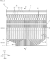
- FIG. 1 is a plan view showing a thermal print head according to a first embodiment of the present disclosure.
- FIG. 2 is a cross-sectional view taken along line II-II in FIG. 1, and shows the printer according to the first embodiment of the present disclosure.
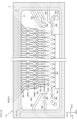
- FIG. 3 is an enlarged plan view of essential parts of the thermal print head according to the first embodiment of the present disclosure.
- FIG. 4 is an enlarged sectional view of a main part taken along line IV-IV in FIG. 3.
- FIG. 5 is an enlarged plan view of essential parts of the thermal print head according to the first embodiment of the present disclosure.
- FIG. 6 is an enlarged plan view of the main parts of the thermal print head according to the first embodiment of the present disclosure.
- FIG. 1 is a plan view showing a thermal print head according to a first embodiment of the present disclosure.
- FIG. 2 is a cross-sectional view taken along line II-II in FIG. 1, and shows the printer according to the first embodiment of the present disclosure.
- FIG. 3 is an enlarged plan view
- FIG. 7 is an enlarged cross-sectional view of a main part taken along line VII-VII in FIG.
- FIG. 8 is a flowchart illustrating a method for manufacturing a thermal print head according to the first embodiment of the present disclosure.
- FIG. 9 is an enlarged cross-sectional view of main parts showing a method for manufacturing a thermal print head according to the first embodiment of the present disclosure.
- FIG. 10 is an enlarged cross-sectional view of main parts showing a method of manufacturing a thermal print head according to the first embodiment of the present disclosure.
- FIG. 11 is an enlarged sectional view of a main part showing a method for manufacturing a thermal print head according to a first embodiment of the present disclosure.
- FIG. 9 is an enlarged cross-sectional view of main part taken along line VII-VII in FIG.
- FIG. 8 is a flowchart illustrating a method for manufacturing a thermal print head according to the first embodiment of the present disclosure.
- FIG. 9 is an enlarged cross-sectional view of main parts showing
- FIG. 12 is an enlarged cross-sectional view of main parts showing a method for manufacturing a thermal print head according to the first embodiment of the present disclosure.
- FIG. 13 is an enlarged plan view of main parts showing a method of manufacturing a thermal print head according to the first embodiment of the present disclosure.
- FIG. 14 is an enlarged sectional view of a main part taken along line XIV-XIV in FIG. 13.
- FIG. 15 is an enlarged plan view of main parts showing a method of manufacturing a thermal print head according to the first embodiment of the present disclosure.
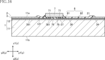
- FIG. 16 is an enlarged sectional view of a main part taken along line XVI-XVI in FIG. 15.
- FIG. 17 is an enlarged plan view of main parts showing a thermal print head according to a second embodiment of the present disclosure.
- FIG. 18 is an enlarged plan view of main parts showing a thermal print head according to a second embodiment of the present disclosure.
- FIG. 19 is an enlarged sectional view of a main part taken along line XIX-XIX in FIG. 17.
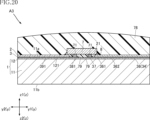
- FIG. 20 is an enlarged sectional view of main parts showing a thermal print head according to a third embodiment of the present disclosure.
- a thing A is formed on a thing B and "a thing A is formed on a thing B” mean “a thing A is formed on a thing B” unless otherwise specified.
- "something A is placed on something B” and “something A is placed on something B” mean "something A is placed on something B” unless otherwise specified.
- a certain surface A faces (one side or the other side of) the direction B is not limited to the case where the angle of the surface A with respect to the direction B is 90 degrees; Including cases where it is tilted to the opposite direction.
- First embodiment: 1 to 7 show a thermal print head A1 and a thermal printer P1 according to a first embodiment of the present disclosure.
- the thermal print head A1 includes a substrate 1, a protective layer 2, a wiring layer 3, a resistor layer 4, a plurality of drive ICs 7, a protective resin 78, a filled resin layer 8, and a heat dissipation member 9.
- the thermal print head A1 is incorporated into a thermal printer P1 that prints on a print medium C1 (see FIG. 2).
- the thermal printer P1 includes a thermal print head A1 and a platen roller B1.
- the platen roller B1 directly faces the thermal print head A1.
- the print medium C1 is sandwiched between the thermal print head A1 and the platen roller B1, and is conveyed in the sub-scanning direction y by the platen roller B1.
- Examples of such print media C1 include thermal paper for creating barcode sheets and receipts.
- a flat rubber platen may be used instead of the platen roller B1. This platen includes a portion of a cylindrical rubber having a large radius of curvature that is arch-shaped in cross-section.
- FIG. 1 is a plan view showing the thermal print head A1.
- FIG. 2 is a cross-sectional view taken along line II-II in FIG. 1, and shows the printer according to the first embodiment of the present disclosure.
- FIG. 3 is an enlarged plan view of the main parts of the thermal print head A1.
- FIG. 4 is an enlarged sectional view of a main part taken along line IV-IV in FIG. 3.
- FIG. 5 is an enlarged plan view of the main parts of the thermal print head A1.
- FIG. 6 is an enlarged plan view of the main parts of the thermal print head A1.
- FIG. 7 is an enlarged cross-sectional view of a main part taken along line VII-VII in FIG. In FIG. 1, the protective layer 2 is omitted.
- FIG. 1 is a plan view showing the thermal print head A1.
- FIG. 2 is a cross-sectional view taken along line II-II in FIG. 1, and shows the printer according to the first embodiment of the present disclosure.
- FIG. 3 is an enlarged plan view
- the protective layer 2 is omitted, and the wiring layer 3 is hatched.
- the protective resin 78 is omitted.
- the protective layer 2 and the filled resin layer 8 are hatched.
- the drive IC 7 and the filled resin layer 8 are shown with imaginary lines.
- the thickness direction of the substrate 1 is defined as the thickness direction z.
- One side in the thickness direction z may be referred to as the z1 side, and the other side may be referred to as the z2 side.
- the main scanning direction x and the sub-scanning direction y are both directions orthogonal to the thickness direction z.
- the print medium C1 is sent from the y2 side to the y1 side in the sub-scanning direction y.
- the y1 side is sometimes referred to as downstream, and the y2 side is sometimes referred to as upstream.
- the substrate 1 has a plate shape that extends long in the main scanning direction x.
- the substrate 1 is a support member that supports a protective layer 2 , a wiring layer 3 , a resistor layer 4 , and a plurality of drive ICs 7 .
- Substrate 1 has base material 11 and glaze layer 12 .
- the base material 11 includes ceramics such as AlN (aluminum nitride), Al 2 O 3 (alumina), and zirconia, and has these ceramics as its main component.
- the thickness of the base material 11 is, for example, 0.6 mm or more and 1.0 mm or less.
- the base material 11 has a rectangular shape that extends in the main scanning direction x when viewed from above.
- the base material 11 has a main surface 11a and a first back surface 11b.
- the main surface 11a and the first back surface 11b are spaced apart in the thickness direction z.
- the main surface 11a faces the z1 side in the thickness direction z.
- the first back surface 11b faces the z2 side in the thickness direction z.
- the main surface 11a is the main surface of the present disclosure, and the first back surface 11b is the back surface of the present disclosure.
- the glaze layer 12 is formed on the main surface 11a of the base material 11. Glaze layer 12 covers main surface 11a. Glaze layer 12 is made of a glass material such as amorphous glass.
- the glaze layer 12 of this example includes a bulged portion 122 and a flat portion 121. Note that the glaze layer 12 may have a configuration including the flat portion 121 and not including the bulging portion 122.
- the bulging portion 122 extends long in the main scanning direction x.
- the bulging portion 122 bulges in the thickness direction z when viewed in the main scanning direction x.
- the bulging portion 122 has an arcuate cross section (yz cross section) taken along a plane perpendicular to the main scanning direction x.
- the bulging portion 122 is provided to make it easier to press a heat generating portion (heat generating portion 41 to be described later) of the resistor layer 4 against the print medium C1.
- the bulging portion 122 is provided as a heat storage layer that accumulates heat from the heat generating portion 41.
- the bulging portion 122 has a larger dimension (maximum dimension) in the thickness direction z than the flat portion 121 .
- the flat portion 121 is formed adjacent to the bulging portion 122, and has a flat surface on the z1 side in the thickness direction z.
- the thickness of the flat portion 121 is, for example, about 2.0 ⁇ m.
- the flat portion 121 is for forming a smooth surface suitable for forming the wiring layer 3 by covering the main surface 11a of the base material 11, which is a relatively rough surface.
- the softening point of the glaze layer 12 is not limited at all.
- the softening point of the flat portion 121 and the softening point of the bulging portion 122 may be different from each other or may be the same.
- the softening point of the flat portion 121 and the bulging portion 122 is, for example, 800° C. or higher and 850° C. or lower, or approximately 680° C., for example.
- the substrate 1 of this embodiment is provided with a plurality of terminals 19.
- the plurality of terminals 19 are arranged in the main scanning direction x, for example, along the edge of the substrate 1 on the y2 side in the sub-scanning direction y.
- the wiring layer 3 constitutes a conduction path for supplying current to the resistor layer 4 .
- the wiring layer 3 is formed of a conductive material.
- the wiring layer 3 contains at least Ag (silver). Further, another part of the wiring layer 3 may contain other than Ag (silver), such as Au (gold).
- Examples of the wiring layer 3 containing Ag (silver) include those formed by printing and firing a paste containing an organic Ag compound or a paste containing Ag particles, glass frit, Pd (palladium), and a resin. .
- the portions of the wiring layer 3 shown in FIGS. 5 to 7, for example, have Ag (silver) as a main component.
- the plurality of strips 32 and the plurality of strips 35 in contact with the resistor layer 4 in the wiring layer 3 may be mainly composed of, for example, Au (gold).
- the thickness of the wiring layer 3 is not limited at all, and is, for example, 1 ⁇ m or more and 10 ⁇ m or less.
- the wiring layer 3 is formed on the glaze layer 12 of the substrate 1.
- the wiring layer 3 has a common electrode 31 and a plurality of individual electrodes 34, as shown in FIGS. 3 and 4. Note that the shape and arrangement of each part of the wiring layer 3 are not limited to the examples shown in FIGS. 3 and 4, and can be configured in various ways.
- the common electrode 31 has a plurality of strip portions 32 and connecting portions 33.
- the connecting portion 33 is disposed near the edge of the substrate 1 on the y1 side in the sub-scanning direction y, and has a band shape extending in the main scanning direction x.
- the plurality of strips 32 each extend from the connecting portion 33 toward the y2 side in the sub-scanning direction y, and are arranged at equal pitches in the main-scanning direction x.
- the auxiliary layer 331 is laminated on the connecting portion 33 in order to reduce the resistance value of the connecting portion 33, but the auxiliary layer 331 does not need to be laminated.
- the auxiliary layer 331 is formed, for example, by printing and baking a paste containing an organic Ag (silver) compound or a paste containing Ag (silver) particles, glass frit, Pd (palladium), and a resin.
- the plurality of individual electrodes 34 are for partially supplying current to the resistor layer 4. Each individual electrode 34 has opposite polarity to the common electrode 31. Each individual electrode 34 extends from the resistor layer 4 toward the drive IC 7. The plurality of individual electrodes 34 are arranged in the main scanning direction x.
- the specific structure of the resistor layer 4 is not limited at all, and each of the plurality of individual electrodes 34 has a strip portion 35, a connecting portion 36, and a first pad portion 37.
- the strip portion 35 extends in the sub-scanning direction y and is strip-shaped when viewed in the thickness direction z.
- Each strip 35 is located between two adjacent strips 32 of the common electrode 31 .
- the distance between the adjacent strip portions 35 of the individual electrodes 34 and the strip portions 32 of the common electrode 31 is, for example, 50 ⁇ m or less.
- the plurality of first pad portions 37 are formed at the ends of the individual electrodes 34 on the y2 side in the sub-scanning direction y.
- the shape of the first pad portion 37 is not limited in any way, and in the illustrated example, it is circular.
- the plurality of first pad sections 37 include a plurality of first pad sections 37A and a plurality of first pad sections 37B.
- the plurality of first pad sections 37A are arranged at equal pitches along the main scanning direction x.
- the first pad portions 37B are arranged on the y2 side of the first pad portion 37A in the sub-scanning direction y, and are arranged at equal pitches along the main-scanning direction x. That is, the plurality of first pad sections 37 are arranged in a staggered manner.
- the first pad portion 37B is connected to a straight portion 361 sandwiched between two adjacent first pad portions 37A.
- the connecting portion 36 is a portion extending from the strip portion 35 toward the plurality of first pad portions 37, as shown in FIGS. 3, 5, and 6.
- the connecting portion 36 includes a straight portion 361, an inclined portion 362, an intermediate portion 363, and a second pad portion 364.
- the straight portion 361 has one end connected to the first pad portion 37 and extends along the sub-scanning direction y.
- the inclined portion 362 is connected to the end of the strip portion 35 on the y2 side in the sub-scanning direction y, and is inclined with respect to the sub-scanning direction y.
- the intermediate portion 363 is interposed between the straight portion 361 and the inclined portion 362.
- the shape of the intermediate portion 363 is not limited at all, and in the illustrated example, it is a bent band-shaped portion.
- the second pad section 364 is interposed between the first pad section 37 and the heat generating section 41, and is formed integrally with the intermediate section 363 in the illustrated example.
- the size and shape of the second pad portion 364 are not limited in any way, and in this embodiment, it is larger than the first pad portion 37 .
- the second pad portion 364 has a substantially pentagonal shape.
- the second pad portions 364 of the connecting portions 36 of the plurality of individual electrodes 34 constitute a plurality of second pad portions 364.
- the arrangement of the plurality of second pad sections 364 is not limited at all.
- the plurality of second pad sections 364 include a plurality of second pad sections 364A and a plurality of second pad sections 364B.
- the plurality of second pad sections 364A are arranged at equal pitches along the main scanning direction x.
- the plurality of second pad sections 364B are arranged at equal pitches along the main scanning direction x on the y2 side of the sub-scanning direction y with respect to the plurality of second pad sections 364A. That is, the plurality of second pad sections 364 are arranged in a staggered manner.
- An intermediate portion 363 integrally formed with the second pad portion 364B is arranged between the adjacent second pad portions 364A.
- An intermediate portion 363 integrally formed with the second pad portion 364A is arranged between the adjacent second pad portions 364B.
- the second pad section 364A and the second pad section 364B are symmetrical about the axis of symmetry extending in the main scanning direction x.
- the plurality of pad sections include a plurality of pad sections 381 and a plurality of pad sections 382 in addition to the plurality of first pad sections 37 described above.
- the wiring layer 3 includes a wiring part 391 and a plurality of wiring parts 392.
- the plurality of pad sections 381 are arranged at equal pitches along the main scanning direction x.
- the plurality of pad sections 381 are arranged on the y2 side in the sub-scanning direction y with respect to the plurality of first pad sections 37.
- the plurality of pad sections 381 are connected to a wiring section 391.
- the wiring section 391 is arranged on the y2 side in the sub-scanning direction y with respect to the plurality of pad sections 381, and has a rectangular shape in the illustrated example.
- the wiring section 391 is, for example, a part of a power supply line for realizing printing by the thermal print head A1.
- the plurality of pad sections 382 are arranged on both sides of the plurality of first pad sections 37 and the plurality of first pad sections 37 in the main scanning direction x.
- the plurality of pad sections 382 are arranged in the main scanning direction x together with the plurality of first pad sections 37A, and the plurality of pad sections 382 are arranged in the main scanning direction x together with the plurality of pad sections 381. and, including.
- the plurality of pad sections 382 include those connected to the plurality of wiring sections 392.
- the resistor layer 4 is formed using a material having higher resistivity than the material constituting the wiring layer 3.
- the resistor layer 4 contains, for example, ruthenium oxide.
- the resistor layer 4 is formed on the bulge 122, as shown in FIGS. 3 and 4.
- the shape of the resistor layer 4 when viewed in the thickness direction z is not limited at all, and in this embodiment, as shown in FIGS. 1 and 3, it is a band shape extending in the main scanning direction x.
- the resistor layer 4 intersects each strip 32 (common electrode 31) and each strip 35 (individual electrode 34).
- the resistor layer 4 is laminated on the z1 side of the plurality of strips 32 and the plurality of strips 35 in the thickness direction z.
- a portion of the resistor layer 4 sandwiched between each strip portion 32 and each strip portion 35 serves as a heat generating portion 41 .
- the plurality of heat generating parts 41 generate heat by being partially energized by the wiring layer 3 .
- Print dots are formed by the heat generated by each heat generating section 41.
- the plurality of heat generating parts 41 are arranged in the main scanning direction x. The greater the number of heat generating parts 41 arranged in the main scanning direction x in the unit length (for example, 1 mm) of the substrate 1 in the main scanning direction x, the greater the dot density of the thermal print head A1.
- the thickness of the resistor layer 4 is, for example, 3 ⁇ m or more and 6 ⁇ m or less.
- the resistor layer 4 is formed on the top of the bulge 122, but may not be formed on the top of the bulge 122.
- the protective layer 2 is for protecting the wiring layer 3, the resistor layer 4, and the like.
- the protective layer 2 may have a single layer structure, or may have a structure in which a plurality of layers are laminated.
- the material of the protective layer 2 is not limited at all.
- An example of the protective layer 2 includes, for example, amorphous glass as a main component.
- a first layer made of amorphous glass and a second layer made of SiAlON, for example, may be laminated.
- SiAlON is a silicon nitride-based engineering ceramic made by synthesizing Si 3 N 4 (silicon nitride) with Al 2 O 3 (alumina) and SiO 2 (silica).
- the second layer is formed by sputtering, for example.
- the second layer may be made of SiC (silicon carbide) instead of SiAlON.
- the protective layer 2 has an opening 21.
- the opening 21 is constituted by a through hole that penetrates the protective layer 2 in the thickness direction z.
- the shape, size, and arrangement of the opening 21 are not limited at all, and are appropriately set depending on the configuration of the plurality of drive ICs 7, the wiring layer 3, and the like.
- the opening 21 is formed in a substantially rectangular shape.
- the opening 21 exposes the plurality of first pad parts 37. That is, the plurality of first pad portions 37 are exposed from the protective layer 2 through the opening 21 and are included in the opening 21 when viewed in the thickness direction z. Furthermore, in this embodiment, the plurality of second pad portions 364 are enclosed within the opening 21 when viewed in the thickness direction z. Furthermore, the plurality of pad portions 381 and the plurality of pad portions 382 are enclosed within the opening 21 when viewed in the thickness direction z.
- the edge of the opening 21 on the y1 side in the sub-scanning direction y intersects with the plurality of individual electrodes 34.
- the edge of the opening 21 on the y1 side in the sub-scanning direction y intersects with the inclined portion 362 or the intermediate portion 363.
- the edge of the opening 21 on the y2 side in the sub-scanning direction y intersects with the wiring portion 391.
- the edges of the opening 21 on both sides in the main scanning direction x intersect with the plurality of wiring portions 392 .
- a plurality of drive ICs 7 are mounted on the substrate 1.
- the plurality of drive ICs 7 are for individually energizing the plurality of heat generating parts 41.
- the drive IC 7 has a plurality of electrodes 71. As shown in FIG. 7, the plurality of electrodes 71 are conductively bonded onto the wiring layer 3 by a bonding layer 79 through the opening 21. Bonding layer 79 is, for example, solder. Thereby, the plurality of drive ICs 7 are electrically connected to the wiring layer 3 and the resistor layer 4.
- the plurality of electrodes 71 are electrically connected to the plurality of first pad sections 37, the plurality of pad sections 381, and the plurality of pad sections 382 through the opening 21 via the bonding layer 79.
- the arrangement of the drive IC 7 is not limited at all, and in this embodiment, the drive IC 7 is entirely enclosed in the opening 21 when viewed in the thickness direction z.
- the power supply control to the plurality of heat generating parts 41 by the plurality of drive ICs 7 follows, for example, a command signal input from the outside of the thermal print head A1 via the plurality of terminals 19.
- the plurality of drive ICs 7 are provided as appropriate depending on the number of the plurality of heat generating parts 41.
- the filled resin layer 8 includes a portion interposed between the substrate 1 (principal surface 11a) and the drive IC 7, and in this embodiment, the filled resin layer 8 includes the flat portion 121 of the glaze layer 12 and the wiring layer 3. This is to fill the gap between the drive IC 7 and the drive IC 7. Furthermore, the filled resin layer 8 covers all of the openings 21. As shown in FIGS. 5 and 6, in this embodiment, the filled resin layer 8 extends from the drive IC 7 when viewed in the thickness direction z, and reaches the edge of the opening 21.
- the filled resin layer 8 is, for example, what is called an underfill agent, and is formed by curing a highly permeable insulating liquid (or paste, etc.).
- the material of the filled resin layer 8 is not limited at all, and conventionally known resins and the like can be used as appropriate.
- the filled resin layer 8 is in contact with a part of the side surface of the drive IC 7. Further, as shown in FIGS. 5 to 7, the filled resin layer 8 has a portion located above the protective layer 2 (a portion covering a part of the protective layer 2).
- the protective resin 78 covers the plurality of drive ICs 7, the filled resin layer 8, and a portion of the protective layer 2.
- the protective resin 78 is made of, for example, an insulating resin and is, for example, black in color. Further, the protective resin 78 may have a structure in which a plurality of layers made of a plurality of types of materials (resin, glass, etc.) are laminated. Further, in FIG. 2, the cross-sectional shape of the protective resin 78 is a shape that gently bulges toward the z1 side in the thickness direction z, but is not limited to this, and can be set to various shapes. Note that the protective resin 78 may be configured to partially cover the filled resin layer 8.
- the heat dissipation member 9 supports the substrate 1, as shown in FIGS. 1 and 2.
- the heat radiating member 9 is for radiating a part of the heat generated by the plurality of heat generating parts 41 to the outside via the substrate 1.
- the heat dissipation member 9 is a block-shaped member made of metal such as Al (aluminum), for example.
- the heat dissipation member 9 has a support surface 91, as shown in FIG.
- the support surface 91 faces the z1 side in the thickness direction z.
- the first back surface 11b of the base material 11 is joined to the support surface 91.
- thermal print head A1 Next, a method for manufacturing the thermal print head A1 will be described below with reference to FIGS. 8 to 16.
- FIG. 8 is a flowchart showing a method for manufacturing the thermal print head A1.
- the manufacturing method of the thermal print head A1 of this embodiment includes a step of preparing a substrate 1, a step of forming a wiring layer 3 and a resistor layer 4, a step of forming the wiring layer 3, and a step of conductively bonding the driving IC 7 to the wiring layer 3. and a step of forming a filled resin layer 8.
- a substrate 1 is prepared.
- the substrate 1 is obtained by forming the glaze layer 12 on the main surface 11a of the base material 11.
- a wiring layer 3 and a resistor layer 4 are formed.
- the wiring layer 3 is formed by, for example, printing a paste containing an organic Ag compound or a paste containing Ag particles, glass frit, Pd (palladium), and a resin on the glaze layer 12, and then firing this. As a result, a conductive film containing Ag (silver) is obtained.
- the wiring layer 3 is obtained by appropriately patterning this conductive film.
- a paste containing, for example, ruthenium oxide is printed along the main scanning direction x so as to cross the plurality of strips 32 and the plurality of strips 35, and is fired. Thereby, the resistor layer 4 is obtained.
- a protective layer 2 is formed.
- the protective layer 2 can be formed, for example, by printing a glass paste and firing it.
- the openings 21 are provided, for example, by not printing glass paste in areas where the openings 21 are to be formed when printing glass paste.
- the plurality of electrodes 71 of the drive IC 7 are electrically connected to the wiring layer 3 through the bonding layer 79.
- the plurality of electrodes 71 are electrically connected to the plurality of first pad sections 37 , the plurality of pad sections 381 , and the plurality of pad sections 381 .
- the drive IC 7 is enclosed in the opening 21 when viewed in the thickness direction z.
- a filled resin layer 8 is formed.
- the first portion 81 is formed.
- An underfill agent or the like is filled into the gap between the glaze layer 12 (principal surface 11a), the wiring layer 3, and the drive IC 7 using a dispenser.
- this underfill agent is attached to a part of the side surface of the drive IC 7.
- this underfill agent remains directly below or near the drive IC 7 when viewed in the thickness direction z, and is spaced apart from the edge of the opening 21 .
- the first portion 81 is formed by appropriately curing the underfill agent.
- the second portion 82 is formed.
- An underfill agent or the like is applied to the region between the first portion 81 and the edge of the opening 21 when viewed in the thickness direction z. That is, the coating is applied to a portion of the opening 21 that is not covered by the first portion 81 .
- the second portion 82 covers, for example, the plurality of second pad portions 364.
- an underfill agent is applied to a portion of the protective layer 2.
- the second portion 82 is formed by appropriately curing the underfill agent, and as a result, the filled resin layer 8 consisting of the first portion 81 and the second portion 82 is formed.
- the filled resin layer 8 may have a structure in which the first part 81 and the second part 82 are distinguishable from each other, or may have a structure in which the first part 81 and the second part 82 are integrated and cannot be distinguished from each other. good. For example, if the first part 81 and the second part 82 are formed with underfill agents of different materials, or if the first part 81 and the second part 82 are cured at different timings. In such cases, the filled resin layer 8 may have a structure in which the first portion 81 and the second portion 82 are distinguishable from each other.
- the thermal print head A1 is obtained by forming the protective resin 78, attaching the substrate 1 to the heat radiating member 9, etc.
- the drive IC 7 is electrically connected to the plurality of first pad portions 37 through the opening 21. All of the openings 21 are closed by the filled resin layer 8. Thereby, it is possible to suppress unintended components contained in the outside air or the like in the operating environment of the thermal print head A1 from corroding the wiring layer 3. Therefore, the occurrence of ion migration in the wiring layer 3 can be suppressed.
- the first part 81 shown in FIGS. 13 and 14 is formed, and the second part 82 shown in FIGS. 15 and 16 is formed.
- the first portion 81 it is possible to sufficiently fill the gap between the substrate 1, the wiring layer 3, and the drive IC 7 with an underfill agent or the like.
- the second portion 82 it is possible to more reliably cover the region of the opening 21 that largely extends from the drive IC 7, that is, the region that is not covered by the first portion 81. Therefore, even if the opening 21 becomes larger, the occurrence of ion migration in the wiring layer 3 can be suppressed.
- a plurality of second pad portions 364 are included in the opening 21.
- the resistance value can be made appropriate by performing laser trimming, for example.
- Second embodiment: 17 to 19 show a thermal print head according to a second embodiment of the present disclosure.
- the thermal print head A2 of this embodiment differs from the embodiments described above mainly in the configurations of the protective layer 2, the wiring layer 3, and the filled resin layer 8.
- each of the connecting portions 36 of the plurality of individual electrodes 34 of the wiring layer 3 does not have the above-mentioned intermediate portion 363 and second pad portion 364.
- the straight portion 361 and the inclined portion 362 are connected.
- the edge of the opening 21 on the y1 side in the sub-scanning direction y intersects with the inclined portion 362 of the connecting portion 36 of the plurality of individual electrodes 34.
- the distance between the edge of the opening 21 on the y1 side in the sub-scanning direction y and the drive IC 7 is smaller than the distance in the thermal print head A1, for example.
- the occurrence of ion migration in the wiring layer 3 can be suppressed.
- the connecting portion 36 does not include the intermediate portion 363 and the second pad portion 364, the opening portion 21 can be reduced. This makes it possible to reduce the area of the portion of the wiring layer 3 exposed from the opening 21, which is preferable for suppressing the occurrence of ion migration in the wiring layer 3.
- the resistance values of the plurality of heat generating parts 41 described above may be measured using, for example, the plurality of first pad parts 37.
- FIG. 20 shows a thermal print head according to a third embodiment of the present disclosure.
- the thermal print head A3 of this embodiment differs from the embodiments described above mainly in the configurations of the protective layer 2, drive IC 7, and filled resin layer 8.
- At least a portion of the edge of the opening 21 overlaps the drive IC 7 when viewed in the thickness direction z. In the illustrated example, all edges of the opening 21 overlap the drive IC 7 when viewed in the thickness direction z.
- the filled resin layer 8 covers all of the openings 21.
- the filled resin layer 8 may be configured only by the first portion 81 described above, for example.
- the opening 21 may be opened so as to appropriately connect the drive IC 7 and the wiring layer 3 to each other.
- the opening 21 is not limited to a configuration that encloses all of the drive IC 7, but may have a configuration that only includes a part of the drive IC 7.
- thermal print head, thermal printer, and method for manufacturing a thermal print head according to the present disclosure are not limited to the embodiments described above.
- the specific configurations of the thermal print head, thermal printer, and method of manufacturing the thermal print head according to the present disclosure can be modified in various designs.
- the present disclosure includes the embodiments described in the appendix below.
- a base material having a main surface and a back surface facing oppositely to each other in the thickness direction; a wiring layer and a resistor layer supported on the main surface; a protective layer that covers a portion of the wiring layer and at least a portion of the resistor layer; a drive IC that controls energization to the resistor layer and is disposed on the main surface; a filled resin layer having a portion interposed between the main surface and the drive IC,
- the wiring layer contains Ag and has a plurality of pad portions,
- the drive IC has a plurality of electrodes,
- the protective layer has an opening that exposes the plurality of pad parts, The plurality of electrodes are electrically connected to the plurality of pad portions through the opening,
- the filled resin layer covers all of the openings of the thermal print head.
- the thermal print head according to appendix 1 further comprising a protective resin that covers the drive IC and at least a portion of the filled resin layer when viewed in the thickness direction.
- Appendix 3. The thermal print head according to appendix 2, wherein the protective resin covers all of the filled resin layer when viewed in the thickness direction.
- Appendix 4. The thermal print head according to any one of Supplementary Notes 1 to 3, wherein all of the drive ICs are included in the opening when viewed in the thickness direction. Appendix 5.
- the thermal print head according to appendix 5 wherein the wiring layer includes a plurality of individual wirings individually connected to the plurality of heat generating parts. Appendix 7. Each of the individual wirings has a first pad portion, The thermal print head according to appendix 6, wherein the plurality of pad portions include the first pad portions of the plurality of individual wirings. Appendix 8. The thermal print head according to appendix 7, wherein the first pad portions of the plurality of individual wirings are arranged along the main scanning direction. Appendix 9. According to appendix 8, each of the individual wirings has a straight part connected to the first pad part and extending in the sub-scanning direction, and an inclined part connected to the straight part and inclined with respect to the sub-scanning direction. thermal print head. Appendix 10.
- Each of the individual wirings has a second pad portion interposed between each of the heat generating portions and the first pad portion,
- Appendix 12 The thermal print head according to appendix 11, wherein the second pad portion is larger than the first pad portion.
- Appendix 13 The thermal print head according to appendix 11 or 12, wherein the second pad portions of the plurality of individual wirings are arranged in a staggered manner along the main scanning direction.
- Appendix 16 The thermal print head according to any one of appendices 1 to 15, further comprising a glaze layer interposed between the base material, the resistor layer, and the wiring layer.
- Appendix 17. A thermal printer comprising the thermal print head described in Appendix 1. Appendix 18.
- the wiring layer contains Ag and has a plurality of pad portions
- the drive IC has a plurality of electrodes
- the protective layer has an opening that exposes the plurality of pad parts, In the step of electrically bonding the driving IC to the wiring layer, electrically bonding the plurality of electrodes to the plurality of pad portions through the opening,
- the step of forming the filled resin layer includes a step of forming a first part interposed between the main surface and the drive IC and spaced apart from an edge of the opening, and a step of forming the first part and the opening.
Landscapes
- Electronic Switches (AREA)
Abstract
L'invention concerne une tête d'impression thermique comprenant un substrat, une couche de câblage et une couche de résistance, une couche de protection, un CI d'attaque et une couche de résine de remplissage ayant une partie interposée entre une surface principale et le CI d'attaque, la couche de câblage comprenant de l'Ag et ayant une pluralité de premiers plots, le CI d'attaque ayant une pluralité d'électrodes, la couche de protection ayant des ouvertures où la pluralité d'électrodes sont exposées, la pluralité d'électrodes étant électriquement connectées à la pluralité de premiers plots à travers les ouvertures et la couche de résine de remplissage remplissant toutes les ouvertures.
Applications Claiming Priority (2)
| Application Number | Priority Date | Filing Date | Title |
|---|---|---|---|
| JP2022106084 | 2022-06-30 | ||
| JP2022-106084 | 2022-06-30 |
Publications (1)
| Publication Number | Publication Date |
|---|---|
| WO2024004658A1 true WO2024004658A1 (fr) | 2024-01-04 |
Family
ID=89382084
Family Applications (1)
| Application Number | Title | Priority Date | Filing Date |
|---|---|---|---|
| PCT/JP2023/022118 WO2024004658A1 (fr) | 2022-06-30 | 2023-06-14 | Tête d'impression thermique, imprimante thermique et procédé de production de tête d'impression thermique |
Country Status (1)
| Country | Link |
|---|---|
| WO (1) | WO2024004658A1 (fr) |
Citations (9)
| Publication number | Priority date | Publication date | Assignee | Title |
|---|---|---|---|---|
| JPS6294846U (fr) * | 1985-12-04 | 1987-06-17 | ||
| US5570123A (en) * | 1995-06-30 | 1996-10-29 | Comtec Information Systems, Inc. | Thermal print head with auxiliary printer head guard |
| JPH09207366A (ja) * | 1996-02-02 | 1997-08-12 | Graphtec Corp | サーマルヘッドおよびその製造方法 |
| WO2012133178A1 (fr) * | 2011-03-25 | 2012-10-04 | 京セラ株式会社 | Tête thermique et imprimante thermique qui en est dotée |
| JP2015193110A (ja) * | 2014-03-31 | 2015-11-05 | ローム株式会社 | サーマルプリントヘッド |
| JP2016185675A (ja) * | 2015-03-27 | 2016-10-27 | 京セラ株式会社 | サーマルヘッドおよびサーマルプリンタ |
| JP2017114050A (ja) * | 2015-12-25 | 2017-06-29 | ローム株式会社 | サーマルプリントヘッド |
| JP2018167439A (ja) * | 2017-03-29 | 2018-11-01 | 京セラ株式会社 | サーマルヘッドおよびサーマルプリンタ |
| JP2019147300A (ja) * | 2018-02-27 | 2019-09-05 | ローム株式会社 | サーマルプリントヘッド |
-
2023
- 2023-06-14 WO PCT/JP2023/022118 patent/WO2024004658A1/fr unknown
Patent Citations (9)
| Publication number | Priority date | Publication date | Assignee | Title |
|---|---|---|---|---|
| JPS6294846U (fr) * | 1985-12-04 | 1987-06-17 | ||
| US5570123A (en) * | 1995-06-30 | 1996-10-29 | Comtec Information Systems, Inc. | Thermal print head with auxiliary printer head guard |
| JPH09207366A (ja) * | 1996-02-02 | 1997-08-12 | Graphtec Corp | サーマルヘッドおよびその製造方法 |
| WO2012133178A1 (fr) * | 2011-03-25 | 2012-10-04 | 京セラ株式会社 | Tête thermique et imprimante thermique qui en est dotée |
| JP2015193110A (ja) * | 2014-03-31 | 2015-11-05 | ローム株式会社 | サーマルプリントヘッド |
| JP2016185675A (ja) * | 2015-03-27 | 2016-10-27 | 京セラ株式会社 | サーマルヘッドおよびサーマルプリンタ |
| JP2017114050A (ja) * | 2015-12-25 | 2017-06-29 | ローム株式会社 | サーマルプリントヘッド |
| JP2018167439A (ja) * | 2017-03-29 | 2018-11-01 | 京セラ株式会社 | サーマルヘッドおよびサーマルプリンタ |
| JP2019147300A (ja) * | 2018-02-27 | 2019-09-05 | ローム株式会社 | サーマルプリントヘッド |
Similar Documents
| Publication | Publication Date | Title |
|---|---|---|
| JP7349549B2 (ja) | サーマルプリントヘッド | |
| US20070040868A1 (en) | Thermal printhead | |
| JP6676369B2 (ja) | サーマルプリントヘッドおよびサーマルプリンタ | |
| WO2024004658A1 (fr) | Tête d'impression thermique, imprimante thermique et procédé de production de tête d'impression thermique | |
| JP7093226B2 (ja) | サーマルプリントヘッド | |
| JP7063442B2 (ja) | サーマルプリントヘッド | |
| JP5080335B2 (ja) | サーマルプリントヘッド | |
| JP3323960B2 (ja) | 薄膜型サーマルプリントヘッド | |
| WO2023210426A1 (fr) | Tête d'impression thermique et imprimante thermique | |
| WO2023223776A1 (fr) | Tête d'impression thermique, imprimante thermique et procédé permettant de fabriquer une tête d'impression thermique | |
| JP7393218B2 (ja) | サーマルプリントヘッドの製造方法およびサーマルプリントヘッド | |
| WO2023228709A1 (fr) | Tête d'impression thermique et imprimante thermique | |
| JP7151054B2 (ja) | サーマルプリントヘッド、および、その製造方法 | |
| WO2023214514A1 (fr) | Tête d'impression thermique, procédé de fabrication de tête d'impression thermique et imprimante thermique | |
| JP7444972B2 (ja) | サーマルヘッドおよびサーマルプリンタ | |
| JP2021115746A (ja) | サーマルプリントヘッド、および、サーマルプリントヘッドの製造方法 | |
| JP7122460B2 (ja) | サーマルヘッドおよびサーマルプリンタ | |
| JP7385481B2 (ja) | サーマルプリントヘッドの製造方法 | |
| JP2023161853A (ja) | サーマルプリントヘッド | |
| JP7219634B2 (ja) | サーマルプリントヘッド | |
| JP7245684B2 (ja) | サーマルプリントヘッド及びサーマルプリントヘッドの製造方法 | |
| JP5329887B2 (ja) | サーマルヘッド | |
| JP2023084582A (ja) | サーマルプリントヘッドの製造方法、サーマルプリントヘッドおよびサーマルプリンタ | |
| JP5260038B2 (ja) | サーマルプリントヘッドおよびその製造方法 | |
| JP2023121941A (ja) | サーマルプリントヘッド |
Legal Events
| Date | Code | Title | Description |
|---|---|---|---|
| 121 | Ep: the epo has been informed by wipo that ep was designated in this application |
Ref document number: 23831106 Country of ref document: EP Kind code of ref document: A1 |