WO2023282000A1 - 炭化珪素単結晶および炭化珪素基板 - Google Patents
炭化珪素単結晶および炭化珪素基板 Download PDFInfo
- Publication number
- WO2023282000A1 WO2023282000A1 PCT/JP2022/023982 JP2022023982W WO2023282000A1 WO 2023282000 A1 WO2023282000 A1 WO 2023282000A1 JP 2022023982 W JP2022023982 W JP 2022023982W WO 2023282000 A1 WO2023282000 A1 WO 2023282000A1
- Authority
- WO
- WIPO (PCT)
- Prior art keywords
- silicon carbide
- section
- main surface
- area
- cross
- Prior art date
- Legal status (The legal status is an assumption and is not a legal conclusion. Google has not performed a legal analysis and makes no representation as to the accuracy of the status listed.)
- Ceased
Links
Images



Classifications
-
- C—CHEMISTRY; METALLURGY
- C30—CRYSTAL GROWTH
- C30B—SINGLE-CRYSTAL GROWTH; UNIDIRECTIONAL SOLIDIFICATION OF EUTECTIC MATERIAL OR UNIDIRECTIONAL DEMIXING OF EUTECTOID MATERIAL; REFINING BY ZONE-MELTING OF MATERIAL; PRODUCTION OF A HOMOGENEOUS POLYCRYSTALLINE MATERIAL WITH DEFINED STRUCTURE; SINGLE CRYSTALS OR HOMOGENEOUS POLYCRYSTALLINE MATERIAL WITH DEFINED STRUCTURE; AFTER-TREATMENT OF SINGLE CRYSTALS OR A HOMOGENEOUS POLYCRYSTALLINE MATERIAL WITH DEFINED STRUCTURE; APPARATUS THEREFOR
- C30B29/00—Single crystals or homogeneous polycrystalline material with defined structure characterised by the material or by their shape
- C30B29/10—Inorganic compounds or compositions
- C30B29/36—Carbides
-
- C—CHEMISTRY; METALLURGY
- C30—CRYSTAL GROWTH
- C30B—SINGLE-CRYSTAL GROWTH; UNIDIRECTIONAL SOLIDIFICATION OF EUTECTIC MATERIAL OR UNIDIRECTIONAL DEMIXING OF EUTECTOID MATERIAL; REFINING BY ZONE-MELTING OF MATERIAL; PRODUCTION OF A HOMOGENEOUS POLYCRYSTALLINE MATERIAL WITH DEFINED STRUCTURE; SINGLE CRYSTALS OR HOMOGENEOUS POLYCRYSTALLINE MATERIAL WITH DEFINED STRUCTURE; AFTER-TREATMENT OF SINGLE CRYSTALS OR A HOMOGENEOUS POLYCRYSTALLINE MATERIAL WITH DEFINED STRUCTURE; APPARATUS THEREFOR
- C30B23/00—Single-crystal growth by condensing evaporated or sublimed materials
-
- C—CHEMISTRY; METALLURGY
- C30—CRYSTAL GROWTH
- C30B—SINGLE-CRYSTAL GROWTH; UNIDIRECTIONAL SOLIDIFICATION OF EUTECTIC MATERIAL OR UNIDIRECTIONAL DEMIXING OF EUTECTOID MATERIAL; REFINING BY ZONE-MELTING OF MATERIAL; PRODUCTION OF A HOMOGENEOUS POLYCRYSTALLINE MATERIAL WITH DEFINED STRUCTURE; SINGLE CRYSTALS OR HOMOGENEOUS POLYCRYSTALLINE MATERIAL WITH DEFINED STRUCTURE; AFTER-TREATMENT OF SINGLE CRYSTALS OR A HOMOGENEOUS POLYCRYSTALLINE MATERIAL WITH DEFINED STRUCTURE; APPARATUS THEREFOR
- C30B25/00—Single-crystal growth by chemical reaction of reactive gases, e.g. chemical vapour-deposition growth
- C30B25/02—Epitaxial-layer growth
- C30B25/18—Epitaxial-layer growth characterised by the substrate
- C30B25/20—Epitaxial-layer growth characterised by the substrate the substrate being of the same materials as the epitaxial layer
Definitions
- the present disclosure relates to silicon carbide single crystals and silicon carbide substrates.
- This application claims priority based on Japanese Patent Application No. 2021-113365 filed on July 8, 2021. All the contents described in the Japanese patent application are incorporated herein by reference.
- Patent Document 1 describes a method for manufacturing a silicon carbide single crystal in which screw dislocations are partially reduced.
- a silicon carbide single crystal according to the present disclosure includes a first main surface, a second main surface opposite to the first main surface, and an outer peripheral surface continuous with each of the first main surface and the second main surface. I have.
- a cross section perpendicular to the thickness direction of the silicon carbide single crystal and located between a first boundary between the first main surface and the outer peripheral surface and a second boundary between the second main surface and the outer peripheral surface is an intermediate cross section. Assuming that the average value of the areal density of threading screw dislocations in the intermediate cross section is the overall average areal density, the intermediate cross section includes a dense region having a areal density of threading screw dislocations that is at least twice the overall average areal density.
- the area of the dense region is 10% or less of the area of the intermediate cross section.
- a cross-section separated from the first boundary toward the second boundary by a distance 0.1 times the distance from the first boundary to the second boundary is defined as the first cross-section, and the cross-section is defined as the first boundary toward the first boundary from the second boundary.
- the linear density of stacking faults in each of the first cross section and the second cross section is 1/cm or less.
- the intermediate cross-section includes sparse and dense regions having an areal density of threading screw dislocations lower than half of the overall average areal density.
- the area of the sparse and dense regions is 12% or more of the area of the intermediate cross section.
- a silicon carbide substrate according to the present disclosure has a main surface. Assuming that the average value of the areal density of threading screw dislocations on the principal surface is the total average areal density, the principal surface includes a dense region having a areal density of threading screw dislocations that is at least twice the total average areal density. The area of the dense region is 10% or less of the area of the main surface. The linear density of stacking faults on the main surface is 1/cm or less.
- the principal surface includes sparse and dense regions having an areal density of threading screw dislocations lower than half of the overall average areal density. The area of the sparse and dense regions is 12% or more of the area of the main surface.
- FIG. 1 is a schematic cross-sectional view showing the configuration of a silicon carbide single crystal according to this embodiment.
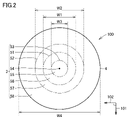
- FIG. 2 is a schematic cross-sectional view taken along line II-II of FIG.
- FIG. 3 is a partially enlarged schematic diagram showing a photoluminescence image of the first cross section.
- FIG. 4 is a partially enlarged schematic diagram showing a photoluminescence image of the second cross section.
- FIG. 5 is a schematic cross-sectional view showing the configuration of the silicon carbide substrate according to this embodiment.
- FIG. 6 is a schematic plan view showing the configuration of the third main surface of the silicon carbide substrate according to this embodiment.
- FIG. 7 is a partially enlarged schematic diagram showing a photoluminescence image of the third main surface.
- FIG. 1 is a schematic cross-sectional view showing the configuration of a silicon carbide single crystal according to this embodiment.
- FIG. 2 is a schematic cross-sectional view taken along line II-II of FIG.
- FIG. 3 is a partially
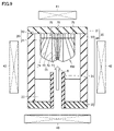
- FIG. 8 is a schematic partial cross-sectional view showing the configuration of the silicon carbide single crystal manufacturing apparatus according to the present embodiment.
- FIG. 9 is a schematic partial cross-sectional view showing a method for manufacturing a silicon carbide single crystal.
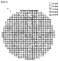
- 10 is a schematic plan view showing surface densities of threading screw dislocations in a plurality of square regions on the third main surface of the silicon carbide substrate according to Sample 1.
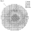
- FIG. 11 is a schematic plan view showing surface densities of threading screw dislocations in a plurality of square regions on the third main surface of the silicon carbide substrate according to sample 2.
- An object of the present disclosure is to provide a silicon carbide single crystal and a silicon carbide substrate that can improve the yield of silicon carbide semiconductor devices. [Effect of the present disclosure] According to the present disclosure, it is possible to provide a silicon carbide single crystal and a silicon carbide substrate that can improve the yield of silicon carbide semiconductor devices.
- Silicon carbide single crystal 100 includes first main surface 1, second main surface 2 opposite to first main surface 1, and each of first main surface 1 and second main surface and an outer peripheral surface 4 that continues to the Perpendicular to the thickness direction of silicon carbide single crystal 100 and intermediate between first boundary 81 between first main surface 1 and outer peripheral surface 4 and second boundary 82 between second main surface 2 and outer peripheral surface 4 , and the average value of the surface density of the threading screw dislocations 70 in the intermediate cross section 3 is defined as the overall average surface density. contains a dense region 55 having an areal density of . The area of the dense region 55 is 10% or less of the area of the intermediate section 3 .
- a cross section separated from the first boundary 81 toward the second boundary 82 by a distance of 0.1 times the distance from the first boundary 81 to the second boundary 82 is defined as a first cross section, and from the second boundary 82 to the first boundary 81 Assuming that the second cross section is a cross section that is 0.1 times the distance from the first boundary 81 to the second boundary 82 toward The density is 1/cm or less.
- the intermediate cross-section 3 includes a sparse and dense region 58 having an areal density of threading screw dislocations 70 lower than half of the overall average areal density. The area of the sparse and dense regions 58 is 12% or more of the area of the intermediate section 3 .
- dense region 55 may include the center of intermediate cross section 3 .
- the area of sparse-dense region 58 may be 30% or more of the area of intermediate cross section 3 .
- intermediate cross section 3 includes first circle 51 having a diameter that is 40% of the diameter of intermediate cross section 3 and It may include an annular region 57 between the second circle 52 having a diameter of 60% of the diameter.
- Each of the center of the first circle 51 and the center of the second circle 52 may be the same as the center of the intermediate section 3 .
- the average surface density of the threading screw dislocations 70 in the annular region 57 may be 1.3 times or more the overall average surface density.
- intermediate cross section 3 may have a diameter of 150 mm or more.
- Silicon carbide substrate 10 includes main surface 61 . If the average value of the areal density of the threading screw dislocations 70 on the main surface 61 is defined as the overall average areal density, the main surface 61 includes a dense region 55 having an areal density of the threading screw dislocations 70 that is at least twice the overall average areal density. . The area of dense region 55 is 10% or less of the area of main surface 61 . The linear density of the stacking faults 5 on the main surface 61 is 1/cm or less. The major surface 61 includes a sparse and dense region 58 having a areal density of threading screw dislocations 70 lower than half of the overall average areal density. The area of the sparse and dense regions 58 is 12% or more of the area of the main surface 61 .
- dense region 55 may include the center of main surface 61 .
- the area of coarsely-dense regions 58 may be 30% or more of the area of main surface 61 .
- main surface 61 includes first circle 51 having a diameter that is 40% of the diameter of main surface 61 and the diameter of main surface 61 may include an annular region 57 between the second circle 52 having a diameter of 60% of .
- Each of the center of the first circle 51 and the center of the second circle 52 may be the same as the center of the major surface 61 .
- the average surface density of the threading screw dislocations 70 in the annular region 57 may be 1.3 times or more the overall average surface density.
- main surface 61 may have a diameter of 150 mm or more.
- FIG. 1 is a schematic cross-sectional view showing the configuration of a silicon carbide single crystal 100 according to this embodiment.
- silicon carbide single crystal 100 according to the present embodiment has first main surface 1 , second main surface 2 , and outer peripheral surface 4 .
- the second major surface 2 is opposite the first major surface 1 .
- the outer peripheral surface 4 continues to each of the first main surface 1 and the second main surface 2 .
- the outer peripheral surface 4 is, for example, a cylindrical surface. Outer peripheral surface 4 surrounds central axis C of silicon carbide single crystal 100 .
- the first major surface 1 is planar, for example.
- the first main surface 1 is, for example, the ⁇ 0001 ⁇ plane or a plane inclined at an off angle with respect to the ⁇ 0001 ⁇ plane.
- the first main surface 1 may be the (0001) plane or a plane inclined by an off angle with respect to the (0001) plane, and the first main surface 1 may be the (000-1) plane.
- it may be a plane inclined at an off angle with respect to the (000-1) plane.
- the off angle may be, for example, 5° or less, or may be 3° or less.
- the off direction may be, for example, the ⁇ 11-20> direction.
- the first main surface 1 extends along each of the first direction 101 and the second direction 102 .
- the first direction 101 is, for example, the ⁇ 1-100> direction.
- the second direction 102 is, for example, the ⁇ 11-20> direction.
- the thickness direction of silicon carbide single crystal 100 is set to third direction 103 .
- the third direction 103 is, for example, the ⁇ 0001> direction.
- the third direction 103 may be a direction inclined by an off angle with respect to the ⁇ 0001> direction.
- Third direction 103 is the same as the growth direction of silicon carbide.
- the third direction 103 may be perpendicular to the first major surface 1 .
- Central axis C of silicon carbide single crystal 100 extends along third direction 103 .
- the second main surface 2 has a central region 24 and an outer peripheral region 25 .
- the outer peripheral region 25 is outside the central region 24 .
- a peripheral region 25 surrounds the central region 24 .
- the central region 24 may be curved to be concave inward. From another point of view, the central region 24 may be curved so as to be recessed toward the first main surface 1 .
- the outer peripheral region 25 may be curved so as to protrude outward. From another point of view, the outer peripheral region 25 may be curved so as to project to the opposite side of the first main surface 1 .
- the thickness (fourth thickness H4) of silicon carbide single crystal 100 is, for example, 1 mm or more and 100 mm or less.
- the lower limit of the fourth thickness H4 is not particularly limited, it may be, for example, 5 mm or more, or 10 mm or more.
- the upper limit of the fourth thickness H4 is not particularly limited, it may be, for example, 80 mm or less, or 60 mm or less.
- a boundary between the first main surface 1 and the outer peripheral surface 4 is defined as a first boundary 81 .
- a boundary between the second main surface 2 and the outer peripheral surface 4 is defined as a second boundary 82 .
- a fourth thickness H4 is the distance from the first boundary 81 to the second boundary 82 . From another point of view, fourth thickness H4 is the thickness of silicon carbide single crystal 100 at the thinnest portion.
- a cross section perpendicular to the thickness direction of silicon carbide single crystal 100 and located midway between first boundary 81 and second boundary 82 is intermediate cross section 3 .
- the distance (the third distance H3) between the first main surface 1 and the intermediate section 3 is half the fourth thickness H4.
- a cross section that is 0.1 times the distance from the first boundary 81 to the second boundary 82 from the first boundary 81 toward the second boundary 82 is defined as a first cross section 11 .
- the distance (first distance H1) between first boundary 81 and first cross section 11 in third direction 103 is 10% of the thickness of silicon carbide single crystal 100 .
- a cross section that is 0.1 times the distance from the first boundary 81 to the second boundary 82 from the second boundary 82 toward the first boundary 81 is defined as a second cross section 12 .
- the distance (second distance H2) between second boundary 82 and second cross section 12 in third direction 103 is 10% of the thickness of silicon carbide single crystal 100 .
- silicon carbide single crystal 100 has a plurality of threading screw dislocations 70 .
- the plurality of threading screw dislocations 70 have, for example, a first threading screw dislocation 71 , a second threading screw dislocation 72 , a third threading screw dislocation 73 , and a fourth threading screw dislocation 74 .
- the first threading screw dislocation 71 extends, for example, along the third direction 103 .
- the first threading screw dislocation 71 may extend along the central axis C.
- the first threading screw dislocation 71 may be located at the center of the first main surface 1 .
- the first threading screw dislocation 71 is exposed on each of the first principal surface 1 and the second principal surface 2 .
- the third threading screw dislocation 73 may be parallel to the first threading screw dislocation 71 .
- the third threading screw dislocation 73 may extend along the third direction 103 .
- the third threading screw dislocation 73 is spaced apart from the center of the first main surface 1 .
- the third threading screw dislocation 73 is exposed on each of the first principal surface 1 and the second principal surface 2 .
- the second threading screw dislocation 72 is inclined with respect to the central axis C.
- Second threading screw dislocation 72 approaches central axis C as silicon carbide single crystal 100 grows. From another point of view, the distance between the second threading screw dislocation 72 and the central axis C in the direction perpendicular to the third direction 103 decreases from the first principal surface 1 toward the second principal surface 2 .
- the distance between the second threading screw dislocation 72 and the central axis C on the first principal surface 1 is greater than the distance between the second threading screw dislocation 72 and the central axis C on the second principal surface 2 .
- the second threading screw dislocation 72 is exposed on each of the first principal surface 1 and the second principal surface 2 .
- the fourth threading screw dislocation 74 is inclined with respect to the central axis C. Fourth threading screw dislocation 74 moves away from central axis C as silicon carbide single crystal 100 grows. From another point of view, the distance between the fourth threading screw dislocation 74 and the central axis C in the direction perpendicular to the third direction 103 increases from the first main surface 1 toward the second main surface 2 . The distance between the fourth threading screw dislocation 74 and the central axis C on the first principal surface 1 is smaller than the distance between the second threading screw dislocation 72 and the central axis C on the second principal surface 2 . The fourth threading screw dislocation 74 is exposed on each of the first principal surface 1 and the second principal surface 2 . The fourth threading screw dislocation 74 may be exposed on the outer peripheral surface 4 .
- FIG. 2 is a schematic cross-sectional view taken along line II-II in FIG.
- the cross-section shown in FIG. 2 is an intermediate cross-section 3 located between the first main surface 1 and the second main surface 2 .
- the shape of the intermediate section 3 is substantially circular.
- the intermediate section 3 is perpendicular to the third direction 103 .
- the fourth diameter W4 is, for example, 150 mm.
- the lower limit of the fourth diameter W4 is not particularly limited, it may be, for example, 150 mm or more, or 200 mm or more.
- the upper limit of the fourth diameter W4 is not particularly limited, but may be, for example, 300 mm or less, or 250 mm or less.
- the intermediate section 3 has, for example, a dense area 55, a non-dense area 56, an annular area 57, and a sparse and dense area 58.
- the dense region 55 has an areal density of the threading screw dislocations 70 that is at least twice the overall average areal density. From another point of view, the areal density of the threading screw dislocations 70 in the dense region 55 is at least twice the overall average areal density.
- Dense region 55 may include center 54 of intermediate cross-section 3 .
- the area of the dense region 55 is 10% or less of the area of the intermediate section 3.
- the upper limit of the area of dense region 55 is not particularly limited, but may be, for example, 9% or less of the area of intermediate cross section 3 or 8% or less of the area of intermediate cross section 3 .
- the lower limit of the area of dense region 55 is not particularly limited, but may be, for example, 1% or more of the area of intermediate cross section 3 or 2% or more of the area of intermediate cross section 3 .
- the outline of the dense area 55 may be circular.
- the outer shape of the dense area 55 is assumed to be the third circle 53 .
- the diameter of the third circle 53 is assumed to be a third diameter W3.
- the upper limit of the third diameter W3 is not particularly limited, but may be, for example, 0.3 times or less than the fourth diameter W4, or may be 0.25 times or less.
- the lower limit of the third diameter W3 is not particularly limited, it may be, for example, 0.1 times or more, or 0.2 times or more the fourth diameter W4.
- the non-dense area 56 is outside the dense area 55 .
- a non-dense region 56 may surround the dense region 55 .
- the non-dense regions 56 have an areal density of threading screw dislocations 70 that is less than twice the overall average areal density. From another point of view, the areal density of the non-dense regions 56 is less than twice the overall average areal density.
- the annular region 57 is between the first circle 51 and the second circle 52.
- the diameter of the first circle 51 is a first diameter W1
- the first diameter W1 has a diameter that is 40% of the diameter of the intermediate section 3 .
- the diameter of the second circle 52 is a second diameter W2
- the second diameter W2 has a diameter that is 60% of the diameter of the intermediate section 3 .
- the center of the first circle 51 and the center of the second circle 52 are each the same as the center of the intermediate section 3 .
- the average surface density of the threading screw dislocations 70 in the annular region 57 is 1.3 times or more the overall average surface density.
- the lower limit of the average areal density of the threading screw dislocations 70 in the annular region 57 is not particularly limited, but may be 1.35 times or more of the overall average areal density, or may be 1.4 times or more. good.
- the upper limit of the average areal density of the threading screw dislocations 70 in the annular region 57 is not particularly limited, but may be 1.9 times or less the overall average areal density, or may be 1.8 times or less. good.
- the sparse-dense region 58 has an areal density of threading screw dislocations 70 lower than half of the overall average areal density.
- the sparse and dense area 58 is located outside the dense area 55, for example.
- the sparse and dense area 58 is located outside the second circle 52, for example.
- the sparse and dense area 58 may be separated from the annular area 57 .
- the sparse and dense area 58 may surround the annular area 57 .
- the area of the sparse and dense regions 58 may be 12% or more of the area of the intermediate cross section 3 .
- the lower limit of the area of the sparse-dense region 58 is not particularly limited, but may be, for example, 20% or more of the area of the intermediate cross section 3, or 25% or more of the area of the intermediate cross section 3, or 25% or more of the area of the intermediate cross section 3. 30% or more of the area of the intermediate section 3 or 35% or more of the area of the intermediate section 3 .
- the upper limit of the area of the sparse-dense region 58 is not particularly limited, but may be, for example, 60% or less of the area of the intermediate cross section 3 or 50% or less of the area of the intermediate cross section 3 .
- FIG. 3 is a partially enlarged schematic diagram showing a photoluminescence image of the first cross section 11.
- FIG. Silicon carbide single crystal 100 according to the present embodiment has stacking faults 5 .
- Stacking faults 5 may extend along the ⁇ 0001 ⁇ plane.
- Stacking faults 5 may extend from first main surface 1 .
- the first main surface 1 may be inclined in the off direction with respect to the ⁇ 0001 ⁇ plane.
- the off direction is the second direction 102, for example.
- the stacking faults 5 may extend in a direction perpendicular to the second direction 102 .
- the second direction 102 is, for example, the ⁇ 11-20> direction.
- the first direction 101 is, for example, the ⁇ 1-100> direction.
- first length A1 the length of the stacking fault 5 in the first direction 101
- second length A2 the length of the stacking fault 5 in the second direction 102
- the linear density of stacking faults 5 in the first cross section 11 is 1/cm or less.
- the upper limit of the linear density of stacking faults 5 in first cross section 11 is not particularly limited, it may be, for example, 0.9/cm or less, or 0.8/cm or less.
- the lower limit of the linear density of stacking faults 5 in first cross section 11 is not particularly limited, it may be, for example, 0.01/cm or more, or 0.1/cm or more.
- FIG. 4 is a partially enlarged schematic diagram showing a photoluminescence image of the second cross section 12.
- the stacking faults 5 may be exposed in the second cross section 12, as shown in FIG.
- the linear density of the stacking faults 5 in the second cross section 12 may be lower than the linear density of the stacking faults 5 in the first cross section 11 .
- the linear density of stacking faults 5 in the second cross section 12 is 1/cm or less.
- the upper limit of the linear density of stacking faults 5 in the second cross section 12 is not particularly limited, it may be, for example, 0.9/cm or less, or 0.8/cm or less.
- the lower limit of the linear density of stacking faults 5 in second cross section 12 is not particularly limited, but may be, for example, 0.01/cm or more, or may be 0.1/cm or more.
- FIG. 5 is a schematic cross-sectional view showing the configuration of silicon carbide substrate 10 according to the present embodiment.
- silicon carbide substrate 10 according to the present embodiment has a third main surface 61 , a fourth main surface 62 and a peripheral edge surface 63 .
- the fourth major surface 62 is on the opposite side of the third major surface 61 .
- the peripheral surface 63 continues to each of the third main surface 61 and the fourth main surface 62 .
- the peripheral surface 63 is, for example, a cylindrical surface. Peripheral edge surface 63 surrounds central axis C of silicon carbide substrate 10 .
- the third main surface 61 is planar, for example.
- the third main surface 61 is, for example, the ⁇ 0001 ⁇ plane or a plane inclined at an off angle with respect to the ⁇ 0001 ⁇ plane.
- the third main surface 61 may be the (0001) plane or a plane inclined by an off angle with respect to the (0001) plane, and the third main surface 61 may be the (000-1) plane.
- it may be a plane inclined at an off angle with respect to the (000-1) plane.
- the off angle may be, for example, 5° or less, or may be 3° or less.
- the off direction may be, for example, the ⁇ 11-20> direction.
- the third main surface 61 extends along each of the first direction 101 and the second direction 102 .
- the first direction 101 is, for example, the ⁇ 1-100> direction.
- the second direction 102 is, for example, the ⁇ 11-20> direction.
- the thickness direction of silicon carbide substrate 10 is defined as third direction 103 .
- the third direction 103 is, for example, the ⁇ 0001> direction.
- the third direction 103 may be a direction inclined by an off angle with respect to the ⁇ 0001> direction.
- Third direction 103 is the same as the growth direction of silicon carbide.
- the third direction 103 may be perpendicular to the third major surface 61 .
- Central axis C of silicon carbide substrate 10 extends along third direction 103 .
- the peripheral surface 63 surrounds the central axis C. As shown in FIG.
- the fourth major surface 62 may be parallel to the third major surface 61 .
- the thickness (fifth thickness H5) of silicon carbide substrate 10 according to the present embodiment is, for example, 100 ⁇ m or more and 700 ⁇ m or less.
- the lower limit of the fifth thickness H5 is not particularly limited, it may be, for example, 200 ⁇ m or more, or may be 300 ⁇ m or more.
- the upper limit of the fifth thickness H5 is not particularly limited, it may be, for example, 600 ⁇ m or less, or 500 ⁇ m or less.
- a fifth thickness H5 is the longest distance between the third main surface 61 and the fourth main surface 62 in the third direction 103 .
- silicon carbide substrate 10 has a plurality of threading screw dislocations 70 .
- the plurality of threading screw dislocations 70 have, for example, a first threading screw dislocation 71 , a second threading screw dislocation 72 , a third threading screw dislocation 73 , and a fourth threading screw dislocation 74 .
- the first threading screw dislocation 71 extends, for example, along the third direction 103 .
- the first threading screw dislocation 71 may extend along the central axis C.
- the first threading screw dislocation 71 may be located at the center of the third main surface 61 .
- the first threading screw dislocation 71 is exposed on each of the third main surface 61 and the fourth main surface 62 .
- the third threading screw dislocation 73 may be parallel to the first threading screw dislocation 71 .
- the third threading screw dislocation 73 may extend along the third direction 103 .
- the third threading screw dislocation 73 is spaced apart from the center of the third main surface 61 .
- the third threading screw dislocation 73 is exposed on each of the third main surface 61 and the fourth main surface 62 .
- the second threading screw dislocation 72 is inclined with respect to the central axis C.
- Second threading screw dislocations 72 approach central axis C as silicon carbide substrate 10 grows. From another point of view, the distance between the second threading screw dislocation 72 and the central axis C in the direction perpendicular to the third direction 103 decreases from the third principal surface 61 toward the fourth principal surface 62 .
- the distance between the second threading screw dislocation 72 and the central axis C on the third principal surface 61 is greater than the distance between the second threading screw dislocation 72 and the central axis C on the fourth principal surface 62 .
- the second threading screw dislocation 72 is exposed on each of the third main surface 61 and the fourth main surface 62 .
- the fourth threading screw dislocation 74 is inclined with respect to the central axis C. Fourth threading screw dislocations 74 move away from central axis C as silicon carbide substrate 10 grows. From another point of view, the distance between the fourth threading screw dislocation 74 and the central axis C in the direction perpendicular to the third direction 103 increases from the third principal surface 61 toward the fourth principal surface 62 . The distance between the fourth threading screw dislocation 74 and the central axis C on the third principal surface 61 is smaller than the distance between the second threading screw dislocation 72 and the central axis C on the fourth principal surface 62 . The fourth threading screw dislocation 74 is exposed on each of the third principal surface 61 and the fourth principal surface 62 . The fourth threading screw dislocation 74 may be exposed on the peripheral surface 63 .
- FIG. 6 is a schematic plan view showing the configuration of the third main surface of the silicon carbide substrate according to this embodiment.
- the peripheral surface 63 has an orientation flat portion 7 and an arcuate portion 8 .
- the arcuate portion 8 continues to the orientation flat portion 7 .
- the orientation flat portion 7 extends along the second direction 102 when viewed in the third direction 103 .
- the fourth diameter W4 is, for example, 150 mm.
- the lower limit of the fourth diameter W4 is not particularly limited, it may be, for example, 150 mm or more, or 200 mm or more.
- the upper limit of the fourth diameter W4 is not particularly limited, but may be, for example, 300 mm or less, or 250 mm or less.
- a fourth diameter W ⁇ b>4 is the longest linear distance between two different points on the peripheral surface 63 when viewed in the third direction 103 .
- the third main surface 61 has, for example, a dense area 55, a non-dense area 56, an annular area 57, and a sparse and dense area 58. If the average value of the areal density of the threading screw dislocations 70 on the third main surface 61 is taken as the total average areal density, the dense region 55 has the areal density of the threading screw dislocations 70 that is at least twice the total average areal density. From another point of view, the areal density of the threading screw dislocations 70 in the dense region 55 is at least twice the overall average areal density. Dense region 55 may include center 54 of third major surface 61 .
- the area of the dense region 55 is 10% or less of the area of the third main surface 61 .
- the upper limit of the area of the dense region 55 is not particularly limited, but may be, for example, 9% or less of the area of the third main surface 61 or 8% or less of the area of the third main surface 61.
- the lower limit of the area of the dense region 55 is not particularly limited, but may be, for example, 1% or more of the area of the third main surface 61 or 2% or more of the area of the third main surface 61. .
- the outline of the dense area 55 may be circular.
- the outer shape of the dense area 55 is assumed to be the third circle 53 .
- the diameter of the third circle 53 is assumed to be a third diameter W3.
- the upper limit of the third diameter W3 is not particularly limited, but may be, for example, 0.3 times or less than the fourth diameter W4, or may be 0.25 times or less.
- the lower limit of the third diameter W3 is not particularly limited, it may be, for example, 0.1 times or more, or 0.2 times or more the fourth diameter W4.
- the non-dense area 56 is outside the dense area 55 .
- a non-dense region 56 may surround the dense region 55 .
- the non-dense regions 56 have an areal density of threading screw dislocations 70 that is less than twice the overall average areal density. From another point of view, the areal density of the non-dense regions 56 is less than twice the overall average areal density.
- the annular region 57 is between the first circle 51 and the second circle 52.
- the diameter of the first circle 51 is a first diameter W1
- the first diameter W1 has a diameter that is 40% of the diameter of the third main surface 61 .
- the diameter of the second circle 52 is a second diameter W2
- the second diameter W2 has a diameter that is 60% of the diameter of the third main surface 61 .
- the center of the first circle 51 and the center of the second circle 52 are each the same as the center of the third main surface 61 .
- the average surface density of the threading screw dislocations 70 in the annular region 57 is 1.3 times or more the overall average surface density.
- the lower limit of the average areal density of the threading screw dislocations 70 in the annular region 57 is not particularly limited, but may be 1.35 times or more of the overall average areal density, or may be 1.4 times or more. good.
- the upper limit of the average areal density of the threading screw dislocations 70 in the annular region 57 is not particularly limited, but may be 1.9 times or less the overall average areal density, or may be 1.8 times or less. good.
- the sparse-dense region 58 has an areal density of threading screw dislocations 70 lower than half of the overall average areal density.
- the sparse and dense area 58 is located outside the dense area 55, for example.
- the sparse and dense area 58 is located outside the second circle 52, for example.
- the sparse and dense area 58 may be separated from the annular area 57 .
- the sparse and dense area 58 may surround the annular area 57 .
- the area of the sparse and dense regions 58 may be 12% or more of the area of the third main surface 61 .
- the lower limit of the area of the sparse and dense region 58 is not particularly limited, but may be, for example, 20% or more of the area of the third main surface 61, or 25% or more of the area of the third main surface 61. , 30% or more of the area of the third main surface 61 or 35% or more of the area of the third main surface 61 .
- the upper limit of the area of the sparse/dense region 58 is not particularly limited, but may be, for example, 60% or less of the area of the third main surface 61 or 50% or less of the area of the third main surface 61 .
- FIG. 7 is a partially enlarged schematic diagram showing a photoluminescence image of the third main surface 61.
- FIG. Silicon carbide substrate 10 according to the present embodiment has stacking faults 5 .
- Stacking faults 5 may extend along the ⁇ 0001 ⁇ plane. As shown in FIG. 3 , the stacking faults 5 are exposed on the third major surface 61 .
- the third main surface 61 may be inclined in the off direction with respect to the ⁇ 0001 ⁇ plane.
- the off direction is the second direction 102, for example.
- the stacking faults 5 may extend in a direction perpendicular to the second direction 102 .
- the second direction 102 is, for example, the ⁇ 11-20> direction.
- the first direction 101 is, for example, the ⁇ 1-100> direction.
- first length A1 the length of the stacking fault 5 in the first direction 101
- second length A2 the length of the stacking fault 5 in the second direction 102
- the linear density of stacking faults 5 on the third main surface 61 is 1/cm or less.
- the upper limit of the linear density of stacking faults 5 on the third main surface 61 is not particularly limited, it may be, for example, 0.9/cm or less, or 0.8/cm or less.
- the lower limit of the linear density of stacking faults 5 on the third main surface 61 is not particularly limited, but may be, for example, 0.01/cm or more, or may be 0.1/cm or more.
- the stacking faults 5 may be exposed on the fourth main surface 62 .
- the linear density of the stacking faults 5 on the fourth main surface 62 may be lower than the linear density of the stacking faults 5 on the third main surface 61 .
- a method for measuring the linear density of stacking faults 5 will be described.
- a photoluminescence imaging device (model number: PLI-200) manufactured by Photon Design Co., Ltd. is used.
- a mercury-xenon lamp for example, is used as the excitation light source.
- the excitation light from the light source passes through a 313 nm bandpass filter and is then applied to the area to be measured.
- Photoluminescence light having a wavelength of 750 nm or more reaches a light receiving element such as a camera. As described above, a photoluminescence image of the area to be measured is captured.
- the emission intensity of the stacking faults 5 is higher than that of the silicon carbide region with a polytype of 4H. Therefore, the stacking fault 5 is displayed as a bright linear region in the photoluminescence image (see FIGS. 3, 4 and 7).
- a photoluminescence image of the surface to be measured is taken while moving silicon carbide substrate 10 in a direction parallel to the surface to be measured (eg, third main surface 61, first cross section 11 or second cross section 12).
- the area of one field of view of the photoluminescence image is, for example, 2.6 mm ⁇ 2.6 mm.
- the photoluminescence image is mapped over the entire area of the surface to be measured.
- a stacking fault 5 is identified in the acquired photoluminescence image.
- the value obtained by dividing the total length of the stacking faults 5 by the area of the measurement region on the surface to be measured is the linear density of the stacking faults 5 .
- the length of the stacking fault 5 is the length (first length A1) of the stacking fault 5 in the longitudinal direction (see FIG. 7).
- the total length of the stacking faults 5 is the total length of each of the multiple stacking faults 5 .
- the areal density of threading screw dislocations 70 is determined using molten potassium hydroxide (KOH), for example.
- KOH molten potassium hydroxide
- the surface to be measured (for example, the third main surface 61, the first cross section 11 or the second cross section 12) is etched with molten KOH.
- the silicon carbide region near the threading screw dislocation 70 exposed on the surface to be measured is etched to form etch pits on the surface to be measured.
- the temperature of the KOH melt is, for example, 500° C. or higher and 550° C. or lower.
- the etching time is 5 minutes or more and 10 minutes or less.
- etch pits on the surface to be measured are observed using a Normarski differential interference microscope.
- a value obtained by dividing the number of etch pits formed on the surface to be measured by the measured area on the surface to be measured corresponds to the areal density of threading screw dislocations 70 .
- the observation field of view is, for example, 0.082 cm ⁇ 0.070 cm.
- a measurement interval is, for example, 5 mm.
- FIG. 8 is a schematic partial cross-sectional view showing the configuration of the silicon carbide single crystal manufacturing apparatus according to the present embodiment.
- the silicon carbide single crystal manufacturing apparatus mainly includes a crucible 30 , a first resistance heater 41 , a second resistance heater 42 and a third resistance heater 43 .
- the crucible 30 has a raw material storage portion 32 and a lid portion 31 .
- the lid portion 31 is arranged on the raw material storage portion 32 .
- the raw material storage portion 32 has a side wall portion 33 , a bottom wall portion 35 and a hollow cylindrical portion 34 .
- the side wall portion 33 is annular.
- the bottom wall portion 35 continues to the side wall portion 33 .
- the hollow tubular portion 34 is arranged in a through hole provided in the bottom wall portion 35 .
- Silicon carbide source material 23 is arranged in a region inside side wall portion 33 and outside hollow tubular portion 34 .
- the first resistance heater 41 is arranged above the lid portion 31 .
- the second resistance heater 42 is arranged so as to surround the side wall portion 33 of the raw material containing portion 32 .
- the third resistance heater 43 is arranged below the bottom wall portion 35 of the raw material storage portion 32 .
- the hollow tubular portion 34 is arranged between the third resistance heater 43 and the lid portion 31 . Radiation heat B from third resistance heater 43 reaches the vicinity of the center of silicon carbide seed substrate 20 through the interior of hollow tubular portion 34 .
- silicon carbide source material 23 is placed in source material accommodating portion 32 .
- Silicon carbide raw material 23 is, for example, powder of polycrystalline silicon carbide.
- Silicon carbide seed substrate 20 is fixed to lid portion 31 using an adhesive (not shown), for example.
- Silicon carbide seed substrate 20 has a growth surface 21 and a mounting surface 22 .
- the mounting surface 22 is opposite the growth surface 21 .
- Growth surface 21 faces silicon carbide source material 23 .
- the mounting surface 22 faces the lid portion 31 .
- the outer peripheral portion of growth surface 21 of silicon carbide seed substrate 20 is arranged to face the surface of silicon carbide source material 23 .
- the hollow tubular portion 34 faces the central portion of the growth surface 21 .
- Silicon carbide seed substrate 20 is, for example, a hexagonal silicon carbide substrate of polytype 4H.
- the diameter of growth surface 21 is, for example, 150 mm.
- the diameter of growth surface 21 may be 150 mm or more.
- Growth plane 21 is, for example, a ⁇ 0001 ⁇ plane or a plane inclined at an off angle of about 5° or less with respect to the ⁇ 0001 ⁇ plane.
- Silicon carbide seed substrate 20 has a plurality of fifth threading screw dislocations 75 . Each of the plurality of fifth threading screw dislocations 75 may extend in a direction perpendicular to the growth surface 21 . As described above, silicon carbide seed substrate 20 and silicon carbide source material 23 are placed in crucible 30 .
- FIG. 9 is a schematic partial cross-sectional view showing a method for manufacturing a silicon carbide single crystal.
- crucible 30 is heated to a temperature of, for example, 2100° C. or higher and 2300° C. or lower. While the temperature of crucible 30 is rising, the pressure of the atmospheric gas in crucible 30 is maintained at, for example, about 80 kPa.
- Atmospheric gas includes inert gas such as argon gas, helium gas, or nitrogen gas.
- the pressure of the atmosphere gas inside the crucible 30 is reduced to, for example, 1.0 kPa.
- silicon carbide source material 23 starts to sublimate, and the sublimated silicon carbide gas is recrystallized on growth surface 21 of silicon carbide seed substrate 20 .
- Silicon carbide single crystal 100 begins to grow on the growth surface of silicon carbide seed substrate 20 . While silicon carbide single crystal 100 is growing, the pressure in crucible 30 is maintained, for example, at approximately 0.1 kPa or more and 3 kPa or less.
- a plurality of fifth threading screw dislocations 75 existing in silicon carbide seed substrate 20 are inherited by silicon carbide single crystal 100 to become a plurality of threading screw dislocations 70 .
- the plurality of threading screw dislocations 70 has a first threading screw dislocation 71 , a second threading screw dislocation 72 , a third threading screw dislocation 73 , and a fourth threading screw dislocation 74 .
- a hollow tubular portion 34 is provided in the silicon carbide single crystal manufacturing apparatus according to the present embodiment. Therefore, radiant heat from the third resistance heater 43 is directly radiated to the central portion of the growth surface. As a result, the temperature of the central portion of the growth surface is higher than the temperature of the peripheral portion surrounding the central portion. Therefore, the growth rate of silicon carbide single crystal 100 in the central portion of the growth surface is lower than the growth rate of silicon carbide single crystal 100 in the outer peripheral portion of the growth surface. As a result, silicon carbide single crystal 100 grows with the central portion of the growth surface (the surface closest to the raw material) of silicon carbide single crystal 100 being depressed (see FIG. 9). Next, silicon carbide single crystal 100 is sliced along a plane perpendicular to the central axis of the silicon carbide single crystal. Thereby, a plurality of silicon carbide substrates 10 are obtained (see FIG. 5).
- Threading screw dislocations 70 tend to extend along the growth direction of silicon carbide single crystal 100 . From another point of view, silicon carbide single crystal 100 tends to elongate in a direction perpendicular to the growth plane. During the crystal growth of silicon carbide single crystal 100, by intentionally recessing central region 24 of the growth surface of silicon carbide single crystal 100, the growth direction of silicon carbide single crystal 100 is changed to the growth surface of silicon carbide single crystal 100. toward the central region 24 of the . As a result, threading screw dislocations 70 extend toward central region 24 of the growth surface of silicon carbide single crystal 100 . That is, threading screw dislocations 70 are concentrated in central region 24 of the growth surface of silicon carbide single crystal 100 .
- threading screw dislocations 70 can be reduced in outer peripheral region 25 around central region 24 of the growth surface (second main surface 2) of silicon carbide single crystal 100 . Therefore, the area of the region of silicon carbide single crystal 100 having a low areal density of threading screw dislocations 70 can be increased. Further, according to the above method, it is not necessary to positively convert threading screw dislocations 70 into stacking faults 5 using a structural conversion layer. Therefore, an increase in the linear density of the stacking faults 5 can be suppressed. Therefore, the yield of silicon carbide semiconductor devices manufactured using silicon carbide single crystal 100 can be improved.
- the cross section perpendicular to the thickness direction of the silicon carbide single crystal 100 and located between the first main surface 1 and the second main surface 2 is the intermediate cross section.
- the average value of the areal density of the threading screw dislocations 70 in the intermediate cross section 3 is defined as the overall average areal density
- the intermediate cross section 3 is a dense region having an areal density of the threading screw dislocations 70 that is at least twice the overall average areal density. 55.
- the area of the dense region 55 is 10% or less of the area of the intermediate section 3 .
- first cross section 11 a cross section at a distance of 0.1 times the thickness of silicon carbide substrate 10 from first main surface 1 is defined as first cross section 11 , and a distance from second main surface 2 is 0.1 times the thickness.
- this cross section is a second cross section 12
- the linear density of the stacking faults 5 in each of the first cross section 11 and the second cross section 12 is 1/cm or less.
- main surface 61 has a through-hole density of at least twice the overall average areal density. It includes a dense region 55 having an areal density of screw dislocations 70 .
- the area of dense region 55 is 10% or less of the area of main surface 61 .
- the linear density of the stacking faults 5 on the main surface 61 is 1/cm or less.
- Silicon carbide single crystals 100 according to sample 1 and sample 2 were prepared. Silicon carbide single crystal 100 according to sample 1 is a comparative example. Silicon carbide single crystal 100 according to sample 2 is an example. Silicon carbide single crystal 100 according to sample 2 was manufactured using the manufacturing apparatus shown in FIG. In the manufacturing apparatus for manufacturing silicon carbide single crystal 100 according to sample 2, hollow cylindrical portion 34 is provided in bottom wall portion 35 of the crucible. On the other hand, silicon carbide single crystal 100 according to sample 1 was manufactured using a conventional manufacturing apparatus in which bottom wall portion 35 of the crucible is not provided with hollow cylindrical portion 34 . The conditions for manufacturing silicon carbide single crystal 100 were as described above.
- a photoluminescence imaging device (model number: PLI-200) manufactured by Photon Design Co., Ltd. was used to measure the linear density of stacking faults 5 in the first cross section 11 of each of the silicon carbide single crystals 100 of Samples 1 and 2. bottom. A photoluminescence image of first cross section 11 was taken while moving silicon carbide single crystal 100 in a direction parallel to first cross section 11 . Similarly, the linear density of stacking faults 5 in second cross section 12 of each of silicon carbide single crystals 100 according to sample 1 and sample 2 was measured. A photoluminescence image of the second cross section 12 was taken while moving the silicon carbide single crystal 100 in a direction parallel to the second cross section 12 .
- a stacking fault 5 was identified in the acquired photoluminescence image.
- a value obtained by dividing the total length of the stacking faults 5 in the first cross section 11 by the area of the first cross section 11 was taken as the linear density of the stacking faults 5 in the first cross section 11 .
- the value obtained by dividing the total length of the stacking faults 5 in the second cross section 12 by the area of the second cross section 12 was taken as the linear density of the stacking faults 5 in the second cross section 12 .
- each of silicon carbide single crystals 100 according to sample 1 and sample 2 was cut with a wire saw.
- silicon carbide substrates 10 according to sample 1 and sample 2 were obtained.
- a photoluminescence image of third main surface 61 was taken while moving silicon carbide substrate 10 in a direction parallel to third main surface 61 .
- a value obtained by dividing the total length of stacking faults 5 on third main surface 61 of silicon carbide substrate 10 by the area of third main surface 61 was taken as the linear density of stacking faults 5 on third main surface 61 .
- the off angle of third main surface 61 of each of silicon carbide substrates 10 according to sample 1 and sample 2 is set to 4°.
- the linear densities of stacking faults 5 in first cross section 11 and second cross section 12 of silicon carbide single crystal 100 according to sample 1 were 0.8/cm and 0.2/cm, respectively. rice field.
- the linear density of stacking faults 5 in third main surface 61 of silicon carbide substrate 10 according to sample 1 obtained by slicing silicon carbide substrate 10 according to sample 1 was 0.9/cm.
- the linear densities of stacking faults 5 in first cross section 11 and second cross section 12 of silicon carbide substrate 10 according to sample 2 were 0.7/cm and 0.3/cm, respectively.
- the linear density of stacking faults 5 in third main surface 61 of silicon carbide substrate 10 according to sample 2 obtained by slicing silicon carbide substrate 10 according to sample 2 was 0.6/cm. From the above results, it was confirmed that the linear density of stacking faults 5 in silicon carbide substrate 10 according to sample 1 is approximately the same as the linear density of stacking faults 5 in silicon carbide substrate 10 according to sample 2 .
- the number of etch pits was determined in each of the square regions. A value obtained by dividing the number of etch pits in the square region by the area of the observation field of the etch pits (0.082 cm ⁇ 0.070 cm) was taken as the surface density of threading screw dislocations 70 in the square region.
- the surface density of threading screw dislocations 70 on third main surface 61 of silicon carbide substrate 10 was obtained by dividing the total surface density of threading screw dislocations 70 in all square regions by the number of square regions.
- FIG. 10 is a schematic plan view showing surface densities of threading screw dislocations 70 in a plurality of square regions of third main surface 61 of silicon carbide substrate 10 according to sample 1.
- the first region is a region where the surface density of threading screw dislocations 70 is less than 520 cm ⁇ 2 .
- the second region is a region where the surface density of threading screw dislocations 70 is 520 cm ⁇ 2 or more and less than 1040 cm ⁇ 2 .
- the third region is a region where the surface density of threading screw dislocations 70 is 1040 cm ⁇ 2 or more and less than 1560 cm ⁇ 2 .
- the fourth region is a region where the surface density of threading screw dislocations 70 is 1560 cm ⁇ 2 or more and less than 2160 cm ⁇ 2 .
- the fifth region is a region where the surface density of threading screw dislocations 70 is 2160 cm ⁇ 2 or more.
- the average value of threading screw dislocations 70 in third main surface 61 of silicon carbide substrate 10 according to sample 1 is 1040 cm ⁇ 2 .
- the average surface density of the threading screw dislocations 70 in the annular region 57 of the third main surface 61 is 1070 cm ⁇ 2 .
- threading screw dislocations 70 are evenly distributed on third main surface 61 of silicon carbide substrate 10 according to sample 1 .
- FIG. 11 is a schematic plan view showing surface densities of threading screw dislocations 70 in a plurality of square regions of third main surface 61 of silicon carbide substrate 10 according to sample 2.
- the sixth region is a region in which the surface density of threading screw dislocations 70 is less than 410 cm ⁇ 2 .
- the seventh region is a region where the surface density of threading screw dislocations 70 is 410 cm ⁇ 2 or more and less than 820 cm ⁇ 2 .
- the eighth region is a region where the surface density of threading screw dislocations 70 is 820 cm ⁇ 2 or more and less than 1230 cm ⁇ 2 .
- the ninth region is a region where the surface density of threading screw dislocations 70 is 1230 cm ⁇ 2 or more and less than 1640 cm ⁇ 2 .
- the tenth region is a region in which the surface density of threading screw dislocations 70 is 1640 cm ⁇ 2 or more.
- the average value of threading screw dislocations 70 in third main surface 61 of silicon carbide substrate 10 according to sample 2 is 820 cm ⁇ 2 .
- the average surface density of the threading screw dislocations 70 in the annular region 57 of the third main surface 61 is 1080 cm ⁇ 2 .
- regions with a high surface density of threading screw dislocations 70 are concentrated near the center of third main surface 61 of silicon carbide substrate 10 according to sample 2 .
- regions with a low areal density of threading screw dislocations 70 are distributed.
- Table 2 shows the area ratio of threading screw dislocations 70 in third main surface 61 of silicon carbide substrate 10 according to sample 1.
- the area ratio of a certain region is a value obtained by dividing the total area of a certain region by the total area of the third main surface 61 .
- the first region is a region having an areal density of threading screw dislocations 70 lower than half of the average value of the areal density of threading screw dislocations 70 on the third main surface 61 .
- the fifth region is a region having an areal density of threading screw dislocations 70 higher than twice the average value of the areal density of threading screw dislocations 70 on the third main surface 61 .
- Table 3 shows the area ratio of threading screw dislocations 70 in the third main surface 61 of the silicon carbide substrate 10 according to Sample 2.
- the sixth region is a region having an areal density of threading screw dislocations 70 lower than half of the average value of the areal density of threading screw dislocations 70 on the third main surface 61 .
- the tenth region is a region having an areal density of threading screw dislocations 70 higher than twice the average value of the areal density of threading screw dislocations 70 on the third main surface 61 .
- the area ratio of the tenth region of silicon carbide substrate 10 according to sample 2 is four times or more the area ratio of the fifth region of silicon carbide substrate 10 according to sample 1. . That is, silicon carbide substrate 10 according to sample 2 has threading screw dislocations higher than twice the average surface density of threading screw dislocations 70 in third main surface 61 as compared with silicon carbide substrate 10 according to sample 1. The area ratio of regions having an areal density of 70 is high.
- the area ratio of the sixth region of silicon carbide substrate 10 according to sample 2 is more than twice the area ratio of the first region of silicon carbide substrate 10 according to sample 1. That is, silicon carbide substrate 10 according to sample 2 has threading screw dislocations 70 lower than half of the average surface density of threading screw dislocations 70 in third main surface 61 as compared with silicon carbide substrate 10 according to sample 1 .
- the area ratio of the region having an areal density of is high. That is, silicon carbide substrate 10 according to sample 2 can have a higher area ratio of a region with a low surface density of threading screw dislocations 70 compared to silicon carbide substrate 10 according to sample 1 .
Landscapes
- Chemical & Material Sciences (AREA)
- Engineering & Computer Science (AREA)
- Crystallography & Structural Chemistry (AREA)
- Materials Engineering (AREA)
- Metallurgy (AREA)
- Organic Chemistry (AREA)
- Inorganic Chemistry (AREA)
- Chemical Kinetics & Catalysis (AREA)
- General Chemical & Material Sciences (AREA)
- Crystals, And After-Treatments Of Crystals (AREA)
Abstract
中間断面は、全体平均面密度の2倍以上の貫通螺旋転位の面密度を有する密集領域を含んでいる。密集領域の面積は、中間断面の面積の10%以下である。第1境界から第2境界に向かって第1境界から第2境界までの距離の0.1倍の距離だけ離れた断面を第1断面とし、第2境界から第1境界に向かって第1境界から第2境界までの距離の0.1倍の距離だけ離れた断面を第2断面とすると、第1断面および第2断面の各々における積層欠陥の線密度は、1/cm以下である。中間断面は、全体平均面密度の半分より低い貫通螺旋転位の面密度を有する疎密領域を含んでいる。疎密領域の面積は、中間断面の面積の12%以上である。
Description
本開示は、炭化珪素単結晶および炭化珪素基板に関する。本出願は、2021年7月8日に出願した日本特許出願である特願2021-113365号に基づく優先権を主張する。当該日本特許出願に記載された全ての記載内容は、参照によって本明細書に援用される。
特開2014-28757号公報(特許文献1)には、部分的に螺旋転位が低減された炭化珪素単結晶の製造方法が記載されている。
本開示に係る炭化珪素単結晶は、第1主面と、第1主面と反対側にある第2主面と、第1主面および第2主面の各々に連なっている外周面とを備えている。炭化珪素単結晶の厚み方向に垂直であって、かつ第1主面と外周面との第1境界と、第2主面と外周面との第2境界との中間に位置する断面を中間断面とし、中間断面における貫通螺旋転位の面密度の平均値を全体平均面密度とすると、中間断面は、全体平均面密度の2倍以上の貫通螺旋転位の面密度を有する密集領域を含んでいる。密集領域の面積は、中間断面の面積の10%以下である。第1境界から第2境界に向かって第1境界から第2境界までの距離の0.1倍の距離だけ離れた断面を第1断面とし、第2境界から第1境界に向かって第1境界から第2境界までの距離の0.1倍の距離だけ離れた断面を第2断面とすると、第1断面および第2断面の各々における積層欠陥の線密度は、1/cm以下である。中間断面は、全体平均面密度の半分より低い貫通螺旋転位の面密度を有する疎密領域を含んでいる。疎密領域の面積は、中間断面の面積の12%以上である。
本開示に係る炭化珪素基板は、主面を備えている。主面における貫通螺旋転位の面密度の平均値を全体平均面密度とすると、主面は、全体平均面密度の2倍以上の貫通螺旋転位の面密度を有する密集領域を含む。密集領域の面積は、主面の面積の10%以下である。主面における積層欠陥の線密度は、1/cm以下である。主面は、全体平均面密度の半分よりも低い貫通螺旋転位の面密度を有する疎密領域を含んでいる。疎密領域の面積は、主面の面積の12%以上である。
[本開示が解決しようとする課題]
上記炭化珪素単結晶の製造方法においては、結晶成長の初期に形成された構造変換層を利用することで、螺旋転位の一部が積層欠陥に変換される。積層欠陥は、炭化珪素単結晶の外周に向かって伸長する。そのため、上記炭化珪素単結晶の製造方法によって製造された炭化珪素単結晶においては、中央付近に多数の螺旋転位が存在し、かつ外周付近に多数の積層欠陥が存在していた。従って、炭化珪素半導体装置の歩留まりを向上することができなかった。
上記炭化珪素単結晶の製造方法においては、結晶成長の初期に形成された構造変換層を利用することで、螺旋転位の一部が積層欠陥に変換される。積層欠陥は、炭化珪素単結晶の外周に向かって伸長する。そのため、上記炭化珪素単結晶の製造方法によって製造された炭化珪素単結晶においては、中央付近に多数の螺旋転位が存在し、かつ外周付近に多数の積層欠陥が存在していた。従って、炭化珪素半導体装置の歩留まりを向上することができなかった。
本開示の目的は、炭化珪素半導体装置の歩留まりを向上可能な炭化珪素単結晶および炭化珪素基板を提供することである。
[本開示の効果]
本開示によれば、炭化珪素半導体装置の歩留まりを向上可能な炭化珪素単結晶および炭化珪素基板を提供することができる。
[本開示の効果]
本開示によれば、炭化珪素半導体装置の歩留まりを向上可能な炭化珪素単結晶および炭化珪素基板を提供することができる。
[本開示の実施形態の概要]
まず、本開示の実施形態の概要について説明する。
まず、本開示の実施形態の概要について説明する。
(1)本開示に係る炭化珪素単結晶100は、第1主面1と、第1主面1と反対側にある第2主面2と、第1主面1および第2主面の各々に連なっている外周面4とを備えている。炭化珪素単結晶100の厚み方向に垂直であって、かつ第1主面1と外周面4との第1境界81と、第2主面2と外周面4との第2境界82との中間に位置する断面を中間断面3とし、中間断面3における貫通螺旋転位70の面密度の平均値を全体平均面密度とすると、中間断面3は、全体平均面密度の2倍以上の貫通螺旋転位70の面密度を有する密集領域55を含む。密集領域55の面積は、中間断面3の面積の10%以下である。第1境界81から第2境界82に向かって第1境界81から第2境界82までの距離の0.1倍の距離だけ離れた断面を第1断面とし、第2境界82から第1境界81に向かって第1境界81から第2境界82までの距離の0.1倍の距離だけ離れた断面を第2断面とすると、第1断面11および第2断面12の各々における積層欠陥5の線密度は、1/cm以下である。中間断面3は、全体平均面密度の半分より低い貫通螺旋転位70の面密度を有する疎密領域58を含んでいる。疎密領域58の面積は、中間断面3の面積の12%以上である。
(2)上記(1)に係る炭化珪素単結晶100において、密集領域55は、中間断面3の中心を含んでいてもよい。
(3)上記(1)または(2)に係る炭化珪素単結晶100において、疎密領域58の面積は、中間断面3の面積の30%以上であってもよい。
(4)上記(1)から(3)のいずれかに係る炭化珪素単結晶100において、中間断面3は、中間断面3の直径の40%の直径を有する第1円51と、中間断面3の直径の60%の直径を有する第2円52との間にある環状領域57を含んでいてもよい。第1円51の中心および第2円52の中心の各々は、中間断面3の中心と同じであってもよい。環状領域57における貫通螺旋転位70の面密度の平均値は、全体平均面密度の1.3倍以上であってもよい。
(5)上記(1)から(4)のいずれかに係る炭化珪素単結晶100において、中間断面3の直径は、150mm以上であってもよい。
(6)本開示に係る炭化珪素基板10は、主面61を備えている。主面61における貫通螺旋転位70の面密度の平均値を全体平均面密度とすると、主面61は、全体平均面密度の2倍以上の貫通螺旋転位70の面密度を有する密集領域55を含む。密集領域55の面積は、主面61の面積の10%以下である。主面61における積層欠陥5の線密度は、1/cm以下である。主面61は、全体平均面密度の半分よりも低い貫通螺旋転位70の面密度を有する疎密領域58を含んでいる。疎密領域58の面積は、主面61の面積の12%以上である。
(7)上記(6)に係る炭化珪素基板10において、密集領域55は、主面61の中心を含んでいてもよい。
(8)上記(6)または(7)に係る炭化珪素基板10において、疎密領域58の面積は、主面61の面積の30%以上であってもよい。
(9)上記(6)から(8)のいずれかに係る炭化珪素基板10において、主面61は、主面61の直径の40%の直径を有する第1円51と、主面61の直径の60%の直径を有する第2円52との間にある環状領域57を含んでいてもよい。第1円51の中心および第2円52の中心の各々は、主面61の中心と同じであってもよい。環状領域57における貫通螺旋転位70の面密度の平均値は、全体平均面密度の1.3倍以上であってもよい。
(10)上記(6)から(9)のいずれかに係る炭化珪素基板10において、主面61の直径は、150mm以上であってもよい。
[本開示の実施形態の詳細]
以下、図面に基づいて本開示の実施形態(以降、本実施形態とも称する)の詳細について説明する。なお、以下の図面において同一または相当する部分には同一の参照番号を付し、その説明は繰返さない。
以下、図面に基づいて本開示の実施形態(以降、本実施形態とも称する)の詳細について説明する。なお、以下の図面において同一または相当する部分には同一の参照番号を付し、その説明は繰返さない。
まず、本実施形態に係る炭化珪素単結晶100の構成について説明する。
図1は、本実施形態に係る炭化珪素単結晶100の構成を示す断面模式図である。図1に示されるように、本実施形態に係る炭化珪素単結晶100は、第1主面1と、第2主面2と、外周面4とを有している。第2主面2は、第1主面1と反対側にある。外周面4は、第1主面1および第2主面2の各々に連なっている。外周面4は、たとえば筒状面である。外周面4は、炭化珪素単結晶100の中心軸Cを取り囲んでいる。第1主面1は、たとえば平面状である。
図1は、本実施形態に係る炭化珪素単結晶100の構成を示す断面模式図である。図1に示されるように、本実施形態に係る炭化珪素単結晶100は、第1主面1と、第2主面2と、外周面4とを有している。第2主面2は、第1主面1と反対側にある。外周面4は、第1主面1および第2主面2の各々に連なっている。外周面4は、たとえば筒状面である。外周面4は、炭化珪素単結晶100の中心軸Cを取り囲んでいる。第1主面1は、たとえば平面状である。
第1主面1は、たとえば{0001}面または{0001}面に対してオフ角だけ傾斜した面である。具体的には、第1主面1は、(0001)面または(0001)面に対してオフ角だけ傾斜した面であってもよいし、第1主面1は、(000-1)面または(000-1)面に対してオフ角だけ傾斜した面であってもよい。オフ角は、たとえば5°以下であってもよいし、3°以下であってもよい。オフ方向は、たとえば<11-20>方向であってもよい。
第1主面1は、第1方向101および第2方向102の各々に沿って延在している。第1方向101は、たとえば<1-100>方向である。第2方向102は、たとえば<11-20>方向である。炭化珪素単結晶100の厚さ方向は、第3方向103とする。第3方向103は、たとえば<0001>方向である。第3方向103は、<0001>方向に対してオフ角だけ傾斜した方向であってもよい。第3方向103は、炭化珪素の成長方向と同じである。第3方向103は、第1主面1に対して垂直であってもよい。炭化珪素単結晶100の中心軸Cは、第3方向103に沿って延在している。
第2主面2は、中央領域24と、外周領域25とを有している。中心軸Cに対して垂直な方向において、外周領域25は、中央領域24の外側にある。外周領域25は、中央領域24を取り囲んでいる。中央領域24は、内側に凹となるように湾曲していてもよい。別の観点から言えば、中央領域24は、第1主面1に向かって凹むように湾曲していてもよい。外周領域25は、外側に凸となるように湾曲していてもよい。別の観点から言えば、外周領域25は、第1主面1の反対側に突出するように湾曲していてもよい。
本実施形態に係る炭化珪素単結晶100の厚み(第4厚みH4)は、たとえば1mm以上100mm以下である。第4厚みH4の下限は、特に限定されないが、たとえば5mm以上であってもよいし、10mm以上であってもよい。第4厚みH4の上限は、特に限定されないが、たとえば80mm以下であってもよいし、60mm以下であってもよい。第1主面1と外周面4との境界は、第1境界81とする。第2主面2と外周面4との境界は、第2境界82とする。第4厚みH4は、第1境界81から第2境界82までの距離とする。別の観点から言えば、第4厚みH4は、最薄部における炭化珪素単結晶100の厚みである。
炭化珪素単結晶100の厚み方向に垂直であって、かつ第1境界81と第2境界82との中間に位置する断面は、中間断面3とする。第3方向103において、第1主面1と中間断面3との距離(第3距離H3)は、第4厚みH4の半分である。第1境界81から第2境界82に向かって第1境界81から第2境界82までの距離の0.1倍の距離だけ離れた断面は、第1断面11とする。言い換えれば、第3方向103において、第1境界81と第1断面11との距離(第1距離H1)は、炭化珪素単結晶100の厚みの10%である。第2境界82から第1境界81に向かって第1境界81から第2境界82までの距離の0.1倍の距離だけ離れた断面は、第2断面12とする。言い換えれば、第3方向103において、第2境界82と第2断面12との距離(第2距離H2)は、炭化珪素単結晶100の厚みの10%である。
図1に示されるように炭化珪素単結晶100は、複数の貫通螺旋転位70を有している。複数の貫通螺旋転位70は、たとえば、第1貫通螺旋転位71と、第2貫通螺旋転位72と、第3貫通螺旋転位73と、第4貫通螺旋転位74とを有している。第1貫通螺旋転位71は、たとえば第3方向103に沿って延在している。第1貫通螺旋転位71は、中心軸Cに沿って延在していてもよい。第1貫通螺旋転位71は、第1主面1の中心に位置していてもよい。第1貫通螺旋転位71は、第1主面1および第2主面2の各々に露出している。第3貫通螺旋転位73は、第1貫通螺旋転位71と平行であってもよい。第3貫通螺旋転位73は、第3方向103に沿って延在していてもよい。第3貫通螺旋転位73は、第1主面1の中心から離間している。第3貫通螺旋転位73は、第1主面1および第2主面2の各々に露出している。
図1に示されるように、第2貫通螺旋転位72は、中心軸Cに対して傾斜している。第2貫通螺旋転位72は、炭化珪素単結晶100が成長するに従って中心軸Cに近づいていく。別の観点から言えば、第1主面1から第2主面2に向かうにつれて、第2貫通螺旋転位72は、第3方向103に垂直な方向における中心軸Cとの距離が小さくなる。第1主面1における第2貫通螺旋転位72と中心軸Cとの距離は、第2主面2における第2貫通螺旋転位72と中心軸Cとの距離よりも大きい。第2貫通螺旋転位72は、第1主面1および第2主面2の各々に露出している。
図1に示されるように、第4貫通螺旋転位74は、中心軸Cに対して傾斜している。第4貫通螺旋転位74は、炭化珪素単結晶100が成長するに従って中心軸Cから遠ざかっていく。別の観点から言えば、第1主面1から第2主面2に向かうにつれて、第4貫通螺旋転位74は、第3方向103に垂直な方向における中心軸Cとの距離が大きくなる。第1主面1における第4貫通螺旋転位74と中心軸Cとの距離は、第2主面2における第2貫通螺旋転位72と中心軸Cとの距離よりも小さい。第4貫通螺旋転位74は、第1主面1および第2主面2の各々に露出している。第4貫通螺旋転位74は、外周面4に露出しいてもよい。
図2は、図1のII-II線に沿った断面模式図である。図2に示される断面は、第1主面1と第2主面2との中間に位置する中間断面3である。中間断面3の形状は、略円形である。中間断面3は、第3方向103に対して垂直である。中間断面3の直径を第4直径W4とすると、第4直径W4は、たとえば150mmである。第4直径W4の下限は、特に限定されないが、たとえば150mm以上であってもよいし、200mm以上であってもよい。第4直径W4の上限は、特に限定されないが、たとえば300mm以下であってもよいし、250mm以下であってもよい。
図2に示されるように、中間断面3は、たとえば、密集領域55と、非密集領域56と、環状領域57と、疎密領域58とを有している。中間断面3における貫通螺旋転位70の面密度の平均値を全体平均面密度とすると、密集領域55は、全体平均面密度の2倍以上の貫通螺旋転位70の面密度を有する。別の観点から言えば、密集領域55における貫通螺旋転位70の面密度は、全体平均面密度の2倍以上である。密集領域55は、中間断面3の中心54を含んでいてもよい。
密集領域55の面積は、中間断面3の面積の10%以下である。密集領域55の面積の上限値は、特に限定されないが、たとえば中間断面3の面積の9%以下であってもよいし、中間断面3の面積の8%以下であってもよい。密集領域55の面積の下限値は、特に限定されないが、たとえば中間断面3の面積の1%以上であってもよいし、中間断面3の面積の2%以上であってもよい。
密集領域55の外形は、円形であってもよい。密集領域55の外形は、第3円53とする。第3円53の直径は、第3直径W3とする。第3直径W3の上限は、特に限定されないが、たとえば第4直径W4の0.3倍以下であってもよいし、0.25倍以下であってもよい。第3直径W3の下限は、特に限定されないが、たとえば第4直径W4の0.1倍以上であってもよいし、0.2倍以上であってもよい。
非密集領域56は、密集領域55の外側にある。非密集領域56は、密集領域55を取り囲んでいてもよい。非密集領域56は、全体平均面密度の2倍未満の貫通螺旋転位70の面密度を有する。別の観点から言えば、非密集領域56の面密度は、全体平均面密度の2倍未満である。
図2に示されるように、環状領域57は、第1円51と第2円52との間にある。第1円51の直径を第1直径W1とすると、第1直径W1は、中間断面3の直径の40%の直径を有する。第2円52の直径を第2直径W2とすると、第2直径W2は、中間断面3の直径の60%の直径を有する。第1円51の中心および第2円52の中心の各々は、中間断面3の中心と同じである。
環状領域57における貫通螺旋転位70の面密度の平均値は、全体平均面密度の1.3倍以上である。環状領域57における貫通螺旋転位70の面密度の平均値の下限値は、特に限定されないが、全体平均面密度の1.35倍以上であってもよいし、1.4倍以上であってもよい。環状領域57における貫通螺旋転位70の面密度の平均値の上限値は、特に限定されないが、全体平均面密度の1.9倍以下であってもよいし、1.8倍以下であってもよい。
疎密領域58は、全体平均面密度の半分より低い貫通螺旋転位70の面密度を有する。疎密領域58は、たとえば密集領域55の外側に位置している。疎密領域58は、たとえば第2円52の外側に位置している。疎密領域58は、環状領域57から離間していてもよい。疎密領域58は、環状領域57を取り囲んでいてもよい。
疎密領域58の面積は、中間断面3の面積の12%以上であってもよい。疎密領域58の面積の下限は、特に限定されないが、たとえば中間断面3の面積の20%以上であってもよいし、中間断面3の面積の25%以上であってもよいし、中間断面3の面積の30%以上であってもよいし、中間断面3の面積の35%以上であってもよい。疎密領域58の面積の上限は、特に限定されないが、たとえば中間断面3の面積の60%以下であってもよいし、中間断面3の面積の50%以下であってもよい。
図3は、第1断面11のフォトルミネッセンス画像を示す一部拡大模式図である。本実施形態に係る炭化珪素単結晶100は、積層欠陥5を有している。積層欠陥5は、{0001}面に沿って延在していてもよい。積層欠陥5は、第1主面1から延在していてもよい。図3に示されているように、積層欠陥5は、第1断面11に露出している。第1主面1は、{0001}面に対してオフ方向に傾斜していてもよい。オフ方向は、たとえば第2方向102である。第3方向103に見て、積層欠陥5は、第2方向102に垂直な方向に延在していてもよい。
第2方向102は、たとえば<11-20>方向である。第1方向101は、たとえば<1-100>方向である。図3に示されるように、第1方向101における積層欠陥5の長さ(第1長さA1)は、第2方向102における積層欠陥5の長さ(第2長さA2)よりも長くてもよい。
第1断面11における積層欠陥5の線密度は、1/cm以下である。第1断面11における積層欠陥5の線密度の上限は、特に限定されないが、たとえば0.9/cm以下であってもよいし、0.8/cm以下であってもよい。第1断面11における積層欠陥5の線密度の下限は、特に限定されないが、たとえば0.01/cm以上であってもよいし、0.1/cm以上であってもよい。
図4は、第2断面12のフォトルミネッセンス画像を示す一部拡大模式図である。図4に示されているように、積層欠陥5は、第2断面12に露出していてもよい。第2断面12における積層欠陥5の線密度は、第1断面11における積層欠陥5の線密度よりも低くてもよい。
第2断面12における積層欠陥5の線密度は、1/cm以下である。第2断面12における積層欠陥5の線密度の上限は、特に限定されないが、たとえば0.9/cm以下であってもよいし、0.8/cm以下であってもよい。第2断面12における積層欠陥5の線密度の下限は、特に限定されないが、たとえば0.01/cm以上であってもよいし、0.1/cm以上であってもよい。
次に、本実施形態に係る炭化珪素基板10の構成について説明する。
図5は、本実施形態に係る炭化珪素基板10の構成を示す断面模式図である。図5に示されるように、本実施形態に係る炭化珪素基板10は、第3主面61と、第4主面62と、周縁面63とを有している。第4主面62は、第3主面61と反対側にある。周縁面63は、第3主面61および第4主面62の各々に連なっている。周縁面63は、たとえば筒状面である。周縁面63は、炭化珪素基板10の中心軸Cを取り囲んでいる。第3主面61は、たとえば平面状である。
図5は、本実施形態に係る炭化珪素基板10の構成を示す断面模式図である。図5に示されるように、本実施形態に係る炭化珪素基板10は、第3主面61と、第4主面62と、周縁面63とを有している。第4主面62は、第3主面61と反対側にある。周縁面63は、第3主面61および第4主面62の各々に連なっている。周縁面63は、たとえば筒状面である。周縁面63は、炭化珪素基板10の中心軸Cを取り囲んでいる。第3主面61は、たとえば平面状である。
第3主面61は、たとえば{0001}面または{0001}面に対してオフ角だけ傾斜した面である。具体的には、第3主面61は、(0001)面または(0001)面に対してオフ角だけ傾斜した面であってもよいし、第3主面61は、(000-1)面または(000-1)面に対してオフ角だけ傾斜した面であってもよい。オフ角は、たとえば5°以下であってもよいし、3°以下であってもよい。オフ方向は、たとえば<11-20>方向であってもよい。
第3主面61は、第1方向101および第2方向102の各々に沿って延在している。第1方向101は、たとえば<1-100>方向である。第2方向102は、たとえば<11-20>方向である。炭化珪素基板10の厚さ方向は、第3方向103とする。第3方向103は、たとえば<0001>方向である。第3方向103は、<0001>方向に対してオフ角だけ傾斜した方向であってもよい。第3方向103は、炭化珪素の成長方向と同じである。第3方向103は、第3主面61に対して垂直であってもよい。炭化珪素基板10の中心軸Cは、第3方向103に沿って延在している。周縁面63は、中心軸Cを取り囲んでいる。第4主面62は、第3主面61と平行であってもよい。
本実施形態に係る炭化珪素基板10の厚み(第5厚みH5)は、たとえば100μm以上700μm以下である。第5厚みH5の下限は、特に限定されないが、たとえば200μm以上であってもよいし、300μm以上であってもよい。第5厚みH5の上限は、特に限定されないが、たとえば600μm以下であってもよいし、500μm以下であってもよい。第5厚みH5は、第3方向103における第3主面61と第4主面62との最長距離とする。
図5に示されるように炭化珪素基板10は、複数の貫通螺旋転位70を有している。複数の貫通螺旋転位70は、たとえば、第1貫通螺旋転位71と、第2貫通螺旋転位72と、第3貫通螺旋転位73と、第4貫通螺旋転位74とを有している。第1貫通螺旋転位71は、たとえば第3方向103に沿って延在している。第1貫通螺旋転位71は、中心軸Cに沿って延在していてもよい。第1貫通螺旋転位71は、第3主面61の中心に位置していてもよい。第1貫通螺旋転位71は、第3主面61および第4主面62の各々に露出している。第3貫通螺旋転位73は、第1貫通螺旋転位71と平行であってもよい。第3貫通螺旋転位73は、第3方向103に沿って延在していてもよい。第3貫通螺旋転位73は、第3主面61の中心から離間している。第3貫通螺旋転位73は、第3主面61および第4主面62の各々に露出している。
図5に示されるように、第2貫通螺旋転位72は、中心軸Cに対して傾斜している。第2貫通螺旋転位72は、炭化珪素基板10が成長するに従って中心軸Cに近づいていく。別の観点から言えば、第3主面61から第4主面62に向かうにつれて、第2貫通螺旋転位72は、第3方向103に垂直な方向における中心軸Cとの距離が小さくなる。第3主面61における第2貫通螺旋転位72と中心軸Cとの距離は、第4主面62における第2貫通螺旋転位72と中心軸Cとの距離よりも大きい。第2貫通螺旋転位72は、第3主面61および第4主面62の各々に露出している。
図5に示されるように、第4貫通螺旋転位74は、中心軸Cに対して傾斜している。第4貫通螺旋転位74は、炭化珪素基板10が成長するに従って中心軸Cから遠ざかっていく。別の観点から言えば、第3主面61から第4主面62に向かうにつれて、第4貫通螺旋転位74は、第3方向103に垂直な方向における中心軸Cとの距離が大きくなる。第3主面61における第4貫通螺旋転位74と中心軸Cとの距離は、第4主面62における第2貫通螺旋転位72と中心軸Cとの距離よりも小さい。第4貫通螺旋転位74は、第3主面61および第4主面62の各々に露出している。第4貫通螺旋転位74は、周縁面63に露出しいてもよい。
図6は、本実施形態に係る炭化珪素基板の第3主面の構成を示す平面模式図である。図6に示されるように、周縁面63は、オリエンテーションフラット部7と、円弧状部8とを有している。円弧状部8は、オリエンテーションフラット部7に連なっている。図6に示されるように、第3方向103に見て、オリエンテーションフラット部7は、第2方向102に沿って延在している。
図6に示されるように、第3主面61の直径を第4直径W4とすると、第4直径W4は、たとえば150mmである。第4直径W4の下限は、特に限定されないが、たとえば150mm以上であってもよいし、200mm以上であってもよい。第4直径W4の上限は、特に限定されないが、たとえば300mm以下であってもよいし、250mm以下であってもよい。第3方向103に見て、第4直径W4は、周縁面63上の異なる2点間の最長直線距離である。
図6に示されるように、第3主面61は、たとえば、密集領域55と、非密集領域56と、環状領域57と、疎密領域58とを有している。第3主面61における貫通螺旋転位70の面密度の平均値を全体平均面密度とすると、密集領域55は、全体平均面密度の2倍以上の貫通螺旋転位70の面密度を有する。別の観点から言えば、密集領域55における貫通螺旋転位70の面密度は、全体平均面密度の2倍以上である。密集領域55は、第3主面61の中心54を含んでいてもよい。
密集領域55の面積は、第3主面61の面積の10%以下である。密集領域55の面積の上限値は、特に限定されないが、たとえば第3主面61の面積の9%以下であってもよいし、第3主面61の面積の8%以下であってもよい。密集領域55の面積の下限値は、特に限定されないが、たとえば第3主面61の面積の1%以上であってもよいし、第3主面61の面積の2%以上であってもよい。
密集領域55の外形は、円形であってもよい。密集領域55の外形は、第3円53とする。第3円53の直径は、第3直径W3とする。第3直径W3の上限は、特に限定されないが、たとえば第4直径W4の0.3倍以下であってもよいし、0.25倍以下であってもよい。第3直径W3の下限は、特に限定されないが、たとえば第4直径W4の0.1倍以上であってもよいし、0.2倍以上であってもよい。
非密集領域56は、密集領域55の外側にある。非密集領域56は、密集領域55を取り囲んでいてもよい。非密集領域56は、全体平均面密度の2倍未満の貫通螺旋転位70の面密度を有する。別の観点から言えば、非密集領域56の面密度は、全体平均面密度の2倍未満である。
図6に示されるように、環状領域57は、第1円51と第2円52との間にある。第1円51の直径を第1直径W1とすると、第1直径W1は、第3主面61の直径の40%の直径を有する。第2円52の直径を第2直径W2とすると、第2直径W2は、第3主面61の直径の60%の直径を有する。第1円51の中心および第2円52の中心の各々は、第3主面61の中心と同じである。
環状領域57における貫通螺旋転位70の面密度の平均値は、全体平均面密度の1.3倍以上である。環状領域57における貫通螺旋転位70の面密度の平均値の下限値は、特に限定されないが、全体平均面密度の1.35倍以上であってもよいし、1.4倍以上であってもよい。環状領域57における貫通螺旋転位70の面密度の平均値の上限値は、特に限定されないが、全体平均面密度の1.9倍以下であってもよいし、1.8倍以下であってもよい。
疎密領域58は、全体平均面密度の半分より低い貫通螺旋転位70の面密度を有する。疎密領域58は、たとえば密集領域55の外側に位置している。疎密領域58は、たとえば第2円52の外側に位置している。疎密領域58は、環状領域57から離間していてもよい。疎密領域58は、環状領域57を取り囲んでいてもよい。
疎密領域58の面積は、第3主面61の面積の12%以上であってもよい。疎密領域58の面積の下限は、特に限定されないが、たとえば第3主面61の面積の20%以上であってもよいし、第3主面61の面積の25%以上であってもよいし、第3主面61の面積の30%以上であってもよいし、第3主面61の面積の35%以上であってもよい。疎密領域58の面積の上限は、特に限定されないが、たとえば第3主面61の面積の60%以下であってもよいし、第3主面61の面積の50%以下であってもよい。
図7は、第3主面61のフォトルミネッセンス画像を示す一部拡大模式図である。本実施形態に係る炭化珪素基板10は、積層欠陥5を有している。積層欠陥5は、{0001}面に沿って延在していてもよい。図3に示されているように、積層欠陥5は、第3主面61に露出している。第3主面61は、{0001}面に対してオフ方向に傾斜していてもよい。オフ方向は、たとえば第2方向102である。第3方向103に見て、積層欠陥5は、第2方向102に垂直な方向に延在していてもよい。
第2方向102は、たとえば<11-20>方向である。第1方向101は、たとえば<1-100>方向である。図7に示されるように、第1方向101における積層欠陥5の長さ(第1長さA1)は、第2方向102における積層欠陥5の長さ(第2長さA2)よりも長くてもよい。
第3主面61における積層欠陥5の線密度は、1/cm以下である。第3主面61における積層欠陥5の線密度の上限は、特に限定されないが、たとえば0.9/cm以下であってもよいし、0.8/cm以下であってもよい。第3主面61における積層欠陥5の線密度の下限は、特に限定されないが、たとえば0.01/cm以上であってもよいし、0.1/cm以上であってもよい。積層欠陥5は、第4主面62に露出していてもよい。第4主面62における積層欠陥5の線密度は、第3主面61における積層欠陥5の線密度よりも低くてもよい。
次に、積層欠陥5の線密度の測定方法について説明する。
積層欠陥5の測定においては、たとえば株式会社フォトンデザイン社製のフォトルミネッセンスイメージング装置(型番:PLI-200)が用いられる。積層欠陥5の被測定領域に対して励起光が照射されると、被測定領域からフォトルミネッセンス光が観測される。励起光源としては、たとえば水銀キセノンランプが使用される。光源からの励起光は、313nmのバンドパスフィルターを通過した後、被測定領域に照射される。750nm以上の波長を有するフォトルミネッセンス光が、カメラ等の受光素子に到達する。以上のように、被測定領域のフォトルミネッセンス画像が撮影される。
積層欠陥5の測定においては、たとえば株式会社フォトンデザイン社製のフォトルミネッセンスイメージング装置(型番:PLI-200)が用いられる。積層欠陥5の被測定領域に対して励起光が照射されると、被測定領域からフォトルミネッセンス光が観測される。励起光源としては、たとえば水銀キセノンランプが使用される。光源からの励起光は、313nmのバンドパスフィルターを通過した後、被測定領域に照射される。750nm以上の波長を有するフォトルミネッセンス光が、カメラ等の受光素子に到達する。以上のように、被測定領域のフォトルミネッセンス画像が撮影される。
積層欠陥5の発光強度は、ポリタイプが4Hの炭化珪素領域の発光強度よりも高い。そのため、フォトルミネッセンス画像において、積層欠陥5は、明るい線状の領域として表示される(図3、図4および図7参照)。たとえば被測定面(たとえば、第3主面61、第1断面11または第2断面12)と平行な方向に炭化珪素基板10を移動させながら、被測定面のフォトルミネッセンス画像が撮影される。フォトルミネッセンス画像の1つの視野の面積は、たとえば2.6mm×2.6mmである。これにより、被測定面の全領域におけるフォトルミネッセンス画像がマッピングされる。取得されたフォトルミネッセンス画像において積層欠陥5が特定される。積層欠陥5の総長を、被測定面における測定領域の面積で除した値が積層欠陥5の線密度である。ここで、積層欠陥5の長さは、長手方向における積層欠陥5の長さ(第1長さA1)である(図7参照)。積層欠陥5が複数ある場合、積層欠陥5の総長とは、複数の積層欠陥5の各々の長さの合計である。
次に、貫通螺旋転位70の面密度の測定方法について説明する。
貫通螺旋転位70の面密度は、たとえば溶融水酸化カリウム(KOH)を用いて決定される。具体的には、被測定面(たとえば、第3主面61、第1断面11または第2断面12)が、溶融KOHによってエッチングされる。これにより、被測定面に露出した貫通螺旋転位70の付近にある炭化珪素領域がエッチングされ、被測定面にエッチピットが形成される。KOH融液の温度は、たとえば500℃以上550℃以下とする。エッチング時間は、5分以上10分以下とする。
貫通螺旋転位70の面密度は、たとえば溶融水酸化カリウム(KOH)を用いて決定される。具体的には、被測定面(たとえば、第3主面61、第1断面11または第2断面12)が、溶融KOHによってエッチングされる。これにより、被測定面に露出した貫通螺旋転位70の付近にある炭化珪素領域がエッチングされ、被測定面にエッチピットが形成される。KOH融液の温度は、たとえば500℃以上550℃以下とする。エッチング時間は、5分以上10分以下とする。
エッチング後、被測定面におけるエッチピットが、ノルマルスキー微分干渉顕微鏡を用いて観察される。被測定面に形成されたエッチピットの数を、被測定面における測定面積で除した値が、貫通螺旋転位70の面密度に対応する。観察視野は、たとえば0.082cm×0.070cmとする。測定間隔は、たとえば5mmとする。
次に、本実施形態に係る炭化珪素単結晶の製造装置の構成について説明する。
図8は、本実施形態に係る炭化珪素単結晶の製造装置の構成を示す一部断面模式図である。図8に示されるように、炭化珪素単結晶の製造装置は、坩堝30と、第1抵抗ヒータ41と、第2抵抗ヒータ42と、第3抵抗ヒータ43とを主に有している。坩堝30は、原料収容部32と、蓋部31とを有している。蓋部31は、原料収容部32上に配置される。
図8は、本実施形態に係る炭化珪素単結晶の製造装置の構成を示す一部断面模式図である。図8に示されるように、炭化珪素単結晶の製造装置は、坩堝30と、第1抵抗ヒータ41と、第2抵抗ヒータ42と、第3抵抗ヒータ43とを主に有している。坩堝30は、原料収容部32と、蓋部31とを有している。蓋部31は、原料収容部32上に配置される。
原料収容部32は、側壁部33と、底壁部35と、中空筒状部34とを有している。側壁部33は、環状である。底壁部35は、側壁部33に連なっている。中空筒状部34は、底壁部35に設けられた貫通孔に配置されている。炭化珪素原料23は、側壁部33の内側であってかつ中空筒状部34の外側の領域において配置される。
第1抵抗ヒータ41は、蓋部31の上方に配置されている。第2抵抗ヒータ42は、原料収容部32の側壁部33を取り囲むように配置されている。第3抵抗ヒータ43は、原料収容部32の底壁部35の下方に配置されている。中空筒状部34は、第3抵抗ヒータ43と、蓋部31との間に配置されている。第3抵抗ヒータ43からの輻射熱Bは、中空筒状部34の内部を通って、炭化珪素種基板20の中央付近に達する。
次に、本実施形態に係る炭化珪素単結晶の製造方法について説明する。
図8に示されるように、炭化珪素原料23が原料収容部32に配置される。炭化珪素原料23は、たとえば多結晶炭化珪素の粉末である。炭化珪素種基板20は、たとえば接着剤(図示せず)を用いて蓋部31に固定される。炭化珪素種基板20は、成長面21と、取付面22とを有している。取付面22は、成長面21と反対側にある。成長面21は、炭化珪素原料23に対向する。取付面22は、蓋部31に対向する。炭化珪素種基板20の成長面21の外周部は、炭化珪素原料23の表面に対向するように配置される。中空筒状部34は、成長面21の中央部に対向している。
図8に示されるように、炭化珪素原料23が原料収容部32に配置される。炭化珪素原料23は、たとえば多結晶炭化珪素の粉末である。炭化珪素種基板20は、たとえば接着剤(図示せず)を用いて蓋部31に固定される。炭化珪素種基板20は、成長面21と、取付面22とを有している。取付面22は、成長面21と反対側にある。成長面21は、炭化珪素原料23に対向する。取付面22は、蓋部31に対向する。炭化珪素種基板20の成長面21の外周部は、炭化珪素原料23の表面に対向するように配置される。中空筒状部34は、成長面21の中央部に対向している。
炭化珪素種基板20は、たとえばポリタイプ4Hの六方晶炭化珪素基板である。成長面21の直径は、たとえば150mmである。成長面21の直径は、150mm以上であってもよい。成長面21は、たとえば{0001}面または{0001}面に対して5°以下程度のオフ角だけ傾斜した面である。炭化珪素種基板20は、複数の第5貫通螺旋転位75を有している。複数の第5貫通螺旋転位75の各々は、成長面21に対して垂直な方向に延在していてもよい。以上のように、炭化珪素種基板20と炭化珪素原料23とが坩堝30に配置される。
図9は、炭化珪素単結晶の製造方法を示す一部断面模式図である。
まず、坩堝30の温度が、たとえば2100℃以上2300℃以下の温度になるまで加熱される。坩堝30の温度が上昇している間、坩堝30内の雰囲気ガスの圧力はたとえば80kPa程度に維持される。雰囲気ガスは、たとえばアルゴンガス、ヘリウムガスまたは窒素ガスなどの不活性ガスを含んでいる。
まず、坩堝30の温度が、たとえば2100℃以上2300℃以下の温度になるまで加熱される。坩堝30の温度が上昇している間、坩堝30内の雰囲気ガスの圧力はたとえば80kPa程度に維持される。雰囲気ガスは、たとえばアルゴンガス、ヘリウムガスまたは窒素ガスなどの不活性ガスを含んでいる。
次に、坩堝30内の雰囲気ガスの圧力が、たとえば1.0kPaまで減圧される。これにより、炭化珪素原料23が昇華を開始し、昇華した炭化珪素ガスが炭化珪素種基板20の成長面21において再結晶化する。炭化珪素種基板20の成長面上において、炭化珪素単結晶100が成長し始める。炭化珪素単結晶100が成長している間、坩堝30内の圧力は、たとえば0.1kPa以上3kPa以下程度に維持される。炭化珪素種基板20に存在していた複数の第5貫通螺旋転位75は、炭化珪素単結晶100に引き継がれて複数の貫通螺旋転位70となる。複数の貫通螺旋転位70は、第1貫通螺旋転位71と、第2貫通螺旋転位72と、第3貫通螺旋転位73と、第4貫通螺旋転位74とを有している。
本実施形態に係る炭化珪素単結晶の製造装置においては、中空筒状部34が設けられている。そのため、第3抵抗ヒータ43からの輻射熱が成長面の中央部に直接輻射される。その結果、成長面の中央部の温度は、中央部の周囲にある外周部の温度よりも高くなる。従って、成長面の中央部における炭化珪素単結晶100の成長速度は、成長面の外周部における炭化珪素単結晶100の成長速度よりも低くなる。結果として、炭化珪素単結晶100の成長面(最も原料に近い面)の中央部が凹んだ状態で、炭化珪素単結晶100が成長する(図9参照)。次に、炭化珪素単結晶の中心軸に垂直な平面に沿って、炭化珪素単結晶100がスライスされる。これにより、複数の炭化珪素基板10が得られる(図5参照)。
次に、本実施形態に係る炭化珪素単結晶100および炭化珪素基板10の作用効果について説明する。
発明者は、積層欠陥5を低減しつつ貫通螺旋転位70を低減する方策について鋭意検討の結果、以下の知見を得て、本実施形態に係る炭化珪素単結晶100、炭化珪素基板10およびそれらの製造方法を見出した。
貫通螺旋転位70は、炭化珪素単結晶100の成長方向に沿って伸長しやすい。別の観点から言えば、炭化珪素単結晶100の成長面に対して垂直な方向に伸長しやすい。炭化珪素単結晶100の結晶成長時において、炭化珪素単結晶100の成長面の中央領域24を意図的に凹ませることにより、炭化珪素単結晶100の成長方向は、炭化珪素単結晶100の成長面の中央領域24に向かって傾く。結果として、貫通螺旋転位70は、炭化珪素単結晶100の成長面の中央領域24に向かって伸長する。つまり、貫通螺旋転位70は、炭化珪素単結晶100の成長面の中央領域24に集中する。
結果として、炭化珪素単結晶100の成長面(第2主面2)の中央領域24の周りにある外周領域25において、貫通螺旋転位70を低減することができる。従って、貫通螺旋転位70の面密度が低い炭化珪素単結晶100の領域の面積を大きくすることができる。また上記方法によれば、構造変換層を用いて、貫通螺旋転位70を積極的に積層欠陥5に変換する必要がない。そのため、積層欠陥5の線密度が増加することを抑制することができる。従って、炭化珪素単結晶100を用いて製造する炭化珪素半導体装置の歩留まりを向上することができる。
本実施形態に係る炭化珪素単結晶100によれば、炭化珪素単結晶100の厚み方向に垂直であって、かつ第1主面1と第2主面2との中間に位置する断面を中間断面3とし、中間断面3における貫通螺旋転位70の面密度の平均値を全体平均面密度とすると、中間断面3は、全体平均面密度の2倍以上の貫通螺旋転位70の面密度を有する密集領域55を含む。密集領域55の面積は、中間断面3の面積の10%以下である。厚み方向において、第1主面1から炭化珪素基板10の厚みの0.1倍の距離だけ離れた断面を第1断面11とし、第2主面2から厚みの0.1倍の距離だけ離れた断面を第2断面12とすると、第1断面11および第2断面12の各々における積層欠陥5の線密度は、1/cm以下である。これにより、積層欠陥5の線密度が低減されかつ貫通螺旋転位70が密集領域55に集中した炭化珪素単結晶100が得られる。そのため、炭化珪素単結晶100を用いて製造する炭化珪素半導体装置の歩留まりを向上することができる。
本実施形態に係る炭化珪素基板10によれば、主面61における貫通螺旋転位70の面密度の平均値を全体平均面密度とすると、主面61は、全体平均面密度の2倍以上の貫通螺旋転位70の面密度を有する密集領域55を含む。密集領域55の面積は、主面61の面積の10%以下である。主面61における積層欠陥5の線密度は、1/cm以下である。これにより、積層欠陥5の線密度が低減されかつ貫通螺旋転位70が密集領域55に集中した炭化珪素基板10が得られる。そのため、炭化珪素基板10を用いて製造する炭化珪素半導体装置の歩留まりを向上することができる。
(サンプル準備)
サンプル1およびサンプル2に係る炭化珪素単結晶100を準備した。サンプル1に係る炭化珪素単結晶100は比較例である。サンプル2に係る炭化珪素単結晶100は実施例である。サンプル2に係る炭化珪素単結晶100は、図8に示される製造装置を使用して製造した。サンプル2に係る炭化珪素単結晶100を製造するための製造装置においては、坩堝の底壁部35に中空筒状部34が設けられている。一方、サンプル1に係る炭化珪素単結晶100は、坩堝の底壁部35に中空筒状部34が設けられていない従来の製造装置を使用して作製した。炭化珪素単結晶100の製造条件は、上述の通りとした。
サンプル1およびサンプル2に係る炭化珪素単結晶100を準備した。サンプル1に係る炭化珪素単結晶100は比較例である。サンプル2に係る炭化珪素単結晶100は実施例である。サンプル2に係る炭化珪素単結晶100は、図8に示される製造装置を使用して製造した。サンプル2に係る炭化珪素単結晶100を製造するための製造装置においては、坩堝の底壁部35に中空筒状部34が設けられている。一方、サンプル1に係る炭化珪素単結晶100は、坩堝の底壁部35に中空筒状部34が設けられていない従来の製造装置を使用して作製した。炭化珪素単結晶100の製造条件は、上述の通りとした。
(評価方法1)
株式会社フォトンデザイン社製のフォトルミネッセンスイメージング装置(型番:PLI-200)を用いて、サンプル1およびサンプル2に係る炭化珪素単結晶100の各々の第1断面11における積層欠陥5の線密度を測定した。第1断面11と平行な方向に炭化珪素単結晶100を移動させながら、第1断面11のフォトルミネッセンス画像を撮影した。同様に、サンプル1およびサンプル2に係る炭化珪素単結晶100の各々の第2断面12における積層欠陥5の線密度を測定した。第2断面12と平行な方向に炭化珪素単結晶100を移動させながら、第2断面12のフォトルミネッセンス画像を撮影した。
株式会社フォトンデザイン社製のフォトルミネッセンスイメージング装置(型番:PLI-200)を用いて、サンプル1およびサンプル2に係る炭化珪素単結晶100の各々の第1断面11における積層欠陥5の線密度を測定した。第1断面11と平行な方向に炭化珪素単結晶100を移動させながら、第1断面11のフォトルミネッセンス画像を撮影した。同様に、サンプル1およびサンプル2に係る炭化珪素単結晶100の各々の第2断面12における積層欠陥5の線密度を測定した。第2断面12と平行な方向に炭化珪素単結晶100を移動させながら、第2断面12のフォトルミネッセンス画像を撮影した。
取得されたフォトルミネッセンス画像において積層欠陥5を特定した。第1断面11における積層欠陥5の総長を、第1断面11の面積で除した値は、第1断面11における積層欠陥5の線密度とした。同様に、第2断面12における積層欠陥5の総長を、第2断面12の面積で除した値は、第2断面12における積層欠陥5の線密度とした。
次に、サンプル1およびサンプル2に係る炭化珪素単結晶100の各々は、ワイヤーソーによって切断された。これにより、サンプル1およびサンプル2に係る炭化珪素基板10が得られた。第3主面61と平行な方向に炭化珪素基板10を移動させながら、第3主面61のフォトルミネッセンス画像を撮影した。炭化珪素基板10の第3主面61における積層欠陥5の総長を、第3主面61の面積で除した値は、第3主面61における積層欠陥5の線密度とした。サンプル1およびサンプル2に係る炭化珪素基板10の各々の第3主面61のオフ角は4°とした。
(評価結果1)

表1に示されるように、サンプル1に係る炭化珪素単結晶100の第1断面11および第2断面12における積層欠陥5の線密度は、それぞれ0.8/cmおよび0.2/cmであった。またサンプル1に係る炭化珪素基板10をスライスすることによって得られたサンプル1に係る炭化珪素基板10の第3主面61における積層欠陥5の線密度は、0.9/cmであった。
サンプル2に係る炭化珪素基板10の第1断面11および第2断面12における積層欠陥5の線密度は、それぞれ0.7/cmおよび0.3/cmであった。またサンプル2に係る炭化珪素基板10をスライスすることによって得られたサンプル2に係る炭化珪素基板10の第3主面61における積層欠陥5の線密度は、0.6/cmであった。以上の結果より、サンプル1に係る炭化珪素基板10における積層欠陥5の線密度は、サンプル2に係る炭化珪素基板10における積層欠陥5の線密度と同程度であることが確認された。
(評価方法2)
次に、溶融KOH法を用いてサンプル1およびサンプル2に係る炭化珪素基板10の第3主面61における貫通螺旋転位70の面密度分布を測定した。具体的には、サンプル1およびサンプル2に係る炭化珪素基板10の第3主面61は、溶融KOHによってエッチングされた。炭化珪素基板10の第3主面61を溶融KOHでエッチング後、貫通螺旋転位70に起因するエッチピットを、ノルマルスキー微分干渉顕微鏡を用いて観察した。エッチピットの観察視野は、0.082cm×0.070cmとした。炭化珪素基板10の第3主面61は、複数の正方領域に区分された。複数の正方領域の各々のサイズは、5mm×5mmとした。複数の正方領域の各々においてエッチピットの数を求めた。正方領域におけるエッチピットの数を、エッチピットの観察視野の面積(0.082cm×0.070cm)で割った値を、当該正方領域における貫通螺旋転位70の面密度とした。全ての正方領域における貫通螺旋転位70の面密度の合計を、正方領域の数で割った値を、炭化珪素基板10の第3主面61における貫通螺旋転位70の面密度とした。
次に、溶融KOH法を用いてサンプル1およびサンプル2に係る炭化珪素基板10の第3主面61における貫通螺旋転位70の面密度分布を測定した。具体的には、サンプル1およびサンプル2に係る炭化珪素基板10の第3主面61は、溶融KOHによってエッチングされた。炭化珪素基板10の第3主面61を溶融KOHでエッチング後、貫通螺旋転位70に起因するエッチピットを、ノルマルスキー微分干渉顕微鏡を用いて観察した。エッチピットの観察視野は、0.082cm×0.070cmとした。炭化珪素基板10の第3主面61は、複数の正方領域に区分された。複数の正方領域の各々のサイズは、5mm×5mmとした。複数の正方領域の各々においてエッチピットの数を求めた。正方領域におけるエッチピットの数を、エッチピットの観察視野の面積(0.082cm×0.070cm)で割った値を、当該正方領域における貫通螺旋転位70の面密度とした。全ての正方領域における貫通螺旋転位70の面密度の合計を、正方領域の数で割った値を、炭化珪素基板10の第3主面61における貫通螺旋転位70の面密度とした。
(評価結果2)
図10は、サンプル1に係る炭化珪素基板10の第3主面61の複数の正方領域における貫通螺旋転位70の面密度を示す平面模式図である。第1領域は、貫通螺旋転位70の面密度が520cm-2未満の領域である。第2領域は、貫通螺旋転位70の面密度が520cm-2以上1040cm-2未満の領域である。第3領域は、貫通螺旋転位70の面密度が1040cm-2以上1560cm-2未満の領域である。第4領域は、貫通螺旋転位70の面密度が1560cm-2以上2160cm-2未満の領域である。第5領域は、貫通螺旋転位70の面密度が2160cm-2以上の領域である。
図10は、サンプル1に係る炭化珪素基板10の第3主面61の複数の正方領域における貫通螺旋転位70の面密度を示す平面模式図である。第1領域は、貫通螺旋転位70の面密度が520cm-2未満の領域である。第2領域は、貫通螺旋転位70の面密度が520cm-2以上1040cm-2未満の領域である。第3領域は、貫通螺旋転位70の面密度が1040cm-2以上1560cm-2未満の領域である。第4領域は、貫通螺旋転位70の面密度が1560cm-2以上2160cm-2未満の領域である。第5領域は、貫通螺旋転位70の面密度が2160cm-2以上の領域である。
サンプル1に係る炭化珪素基板10の第3主面61における貫通螺旋転位70の平均値は、1040cm-2である。第3主面61の環状領域57における貫通螺旋転位70の面密度の平均値は、1070cm-2である。図10に示されるように、サンプル1に係る炭化珪素基板10の第3主面61においては、貫通螺旋転位70は万遍なく分布している。
図11は、サンプル2に係る炭化珪素基板10の第3主面61の複数の正方領域における貫通螺旋転位70の面密度を示す平面模式図である。第6領域は、貫通螺旋転位70の面密度が410cm-2未満の領域である。第7領域は、貫通螺旋転位70の面密度が410cm-2以上820cm-2未満の領域である。第8領域は、貫通螺旋転位70の面密度が820cm-2以上1230cm-2未満の領域である。第9領域は、貫通螺旋転位70の面密度が1230cm-2以上1640cm-2未満の領域である。第10領域は、貫通螺旋転位70の面密度が1640cm-2以上の領域である。
サンプル2に係る炭化珪素基板10の第3主面61における貫通螺旋転位70の平均値は、820cm-2である。第3主面61の環状領域57における貫通螺旋転位70の面密度の平均値は、1080cm-2である。図11に示されるように、サンプル2に係る炭化珪素基板10の第3主面61の中央付近おいては、貫通螺旋転位70の面密度の高い領域が集中している。一方、第3主面61の外周付近おいては、貫通螺旋転位70の面密度の低い領域が分布している。
表2は、サンプル1に係る炭化珪素基板10の第3主面61における貫通螺旋転位70の面積割合を示している。ある領域の面積割合とは、ある領域の合計面積を第3主面61の全面積で除した値である。第1領域は、第3主面61における貫通螺旋転位70の面密度の平均値の半分よりも低い貫通螺旋転位70の面密度を有する領域である。第5領域は、第3主面61における貫通螺旋転位70の面密度の平均値の2倍よりも高い貫通螺旋転位70の面密度を有する領域である。
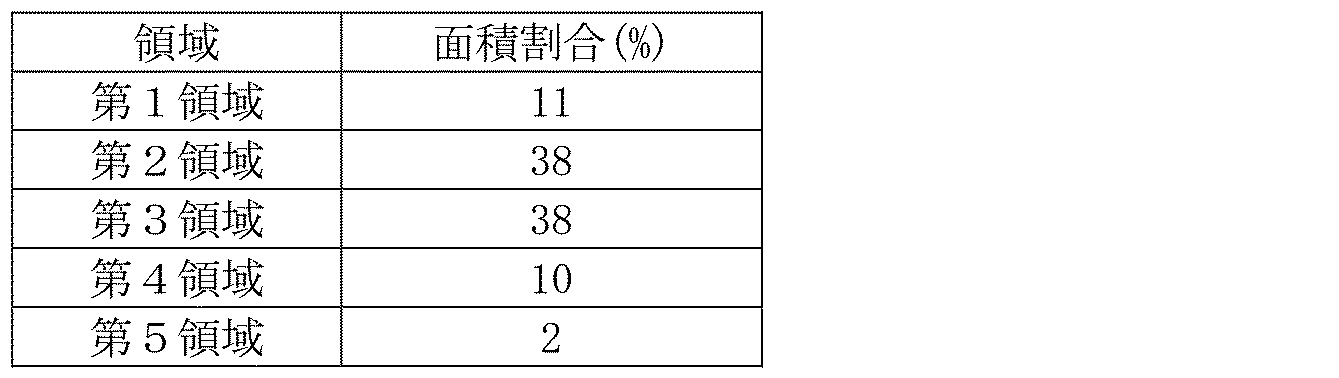
表3は、サンプル2に係る炭化珪素基板10の第3主面61における貫通螺旋転位70の面積割合を示している。第6領域は、第3主面61における貫通螺旋転位70の面密度の平均値の半分よりも低い貫通螺旋転位70の面密度を有する領域である。第10領域は、第3主面61における貫通螺旋転位70の面密度の平均値の2倍よりも高い貫通螺旋転位70の面密度を有する領域である。

表2と表3とを比較すると、サンプル2に係る炭化珪素基板10の第10領域の面積割合は、サンプル1に係る炭化珪素基板10の第5領域の面積割合の4倍以上となっている。つまり、サンプル2に係る炭化珪素基板10は、サンプル1に係る炭化珪素基板10と比較して、第3主面61における貫通螺旋転位70の面密度の平均値の2倍よりも高い貫通螺旋転位70の面密度を有する領域の面積割合が高い。
一方、サンプル2に係る炭化珪素基板10の第6領域の面積割合は、サンプル1に係る炭化珪素基板10の第1領域の面積割合の2倍以上となっている。つまり、サンプル2に係る炭化珪素基板10は、サンプル1に係る炭化珪素基板10と比較して、第3主面61における貫通螺旋転位70の面密度の平均値の半分よりも低い貫通螺旋転位70の面密度を有する領域の面積割合が高い。つまり、サンプル2に係る炭化珪素基板10は、サンプル1に係る炭化珪素基板10と比較して、貫通螺旋転位70の面密度が低い領域の面積割合を高くすることができる。
今回開示された実施の形態および実施例はすべての点で例示であって、制限的なものではないと考えられるべきである。本発明の範囲は上記した説明ではなくて請求の範囲によって示され、請求の範囲と均等の意味、および範囲内でのすべての変更が含まれることが意図される。
1 第1主面、2 第2主面、3 中間断面、4 外周面、5 積層欠陥、7 オリエンテーションフラット部、8 円弧状部、10 炭化珪素基板、11 第1断面、12 第2断面、20 炭化珪素種基板、21 成長面、22 取付面、23 炭化珪素原料、24 中央領域、25 外周領域、30 坩堝、31 蓋部、32 原料収容部、33 側壁部、34 中空筒状部、35 底壁部、41 第1抵抗ヒータ、42 第2抵抗ヒータ、43 第3抵抗ヒータ、51 第1円、52 第2円、53 第3円、54 中心、55 密集領域、56 非密集領域、57 環状領域、58 疎密領域、61 第3主面(主面)、62 第4主面、63 周縁面、70 貫通螺旋転位、71 第1貫通螺旋転位、72 第2貫通螺旋転位、73 第3貫通螺旋転位、74 第4貫通螺旋転位、75 第5貫通螺旋転位、81 第1境界、82 第2境界、100 炭化珪素単結晶、101 第1方向、102 第2方向、103 第3方向、A1 第1長さ、A2 第2長さ、B 輻射熱、C 中心軸、H1 第1距離、H2 第2距離、H3 第3距離、H4 第4厚み、H5 第5厚み、W1 第1直径、W2 第2直径、W3 第3直径、W4 第4直径。
Claims (10)
- 第1主面と、前記第1主面と反対側にある第2主面と、前記第1主面および前記第2主面の各々に連なっている外周面とを備えた炭化珪素単結晶であって、
前記炭化珪素単結晶の厚み方向に垂直であって、かつ前記第1主面と前記外周面との第1境界と、前記第2主面と前記外周面との第2境界との中間に位置する断面を中間断面とし、前記中間断面における貫通螺旋転位の面密度の平均値を全体平均面密度とすると、前記中間断面は、前記全体平均面密度の2倍以上の貫通螺旋転位の面密度を有する密集領域を含み、
前記密集領域の面積は、前記中間断面の面積の10%以下であり、
前記第1境界から前記第2境界に向かって前記第1境界から前記第2境界までの距離の0.1倍の距離だけ離れた断面を第1断面とし、前記第2境界から前記第1境界に向かって前記第1境界から前記第2境界までの距離の0.1倍の距離だけ離れた断面を第2断面とすると、前記第1断面および前記第2断面の各々における積層欠陥の線密度は、1/cm以下であり、
前記中間断面は、前記全体平均面密度の半分より低い貫通螺旋転位の面密度を有する疎密領域を含み、
前記疎密領域の面積は、前記中間断面の面積の12%以上である、炭化珪素単結晶。 - 前記密集領域は、前記中間断面の中心を含む、請求項1に記載の炭化珪素単結晶。
- 前記疎密領域の面積は、前記中間断面の面積の30%以上である、請求項1または請求項2に記載の炭化珪素単結晶。
- 前記中間断面は、前記中間断面の直径の40%の直径を有する第1円と、前記中間断面の直径の60%の直径を有する第2円との間にある環状領域を含み、
前記第1円の中心および前記第2円の中心の各々は、前記中間断面の中心と同じであり、
前記環状領域における貫通螺旋転位の面密度の平均値は、前記全体平均面密度の1.3倍以上である、請求項1から請求項3のいずれか1項に記載の炭化珪素単結晶。 - 前記中間断面の直径は、150mm以上である、請求項1から請求項4のいずれか1項に記載の炭化珪素単結晶。
- 主面を備えた炭化珪素基板であって、
前記主面における貫通螺旋転位の面密度の平均値を全体平均面密度とすると、前記主面は、前記全体平均面密度の2倍以上の貫通螺旋転位の面密度を有する密集領域を含み、
前記密集領域の面積は、前記主面の面積の10%以下であり、
前記主面における積層欠陥の線密度は、1/cm以下であり、
前記主面は、前記全体平均面密度の半分よりも低い貫通螺旋転位の面密度を有する疎密領域を含み、
前記疎密領域の面積は、前記主面の面積の12%以上である、炭化珪素基板。 - 前記密集領域は、前記主面の中心を含む、請求項6に記載の炭化珪素基板。
- 前記疎密領域の面積は、前記主面の面積の30%以上である、請求項6または請求項7に記載の炭化珪素基板。
- 前記主面は、前記主面の直径の40%の直径を有する第1円と、前記主面の直径の60%の直径を有する第2円との間にある環状領域を含み、
前記第1円の中心および前記第2円の中心の各々は、前記主面の中心と同じであり、
前記環状領域における貫通螺旋転位の面密度の平均値は、前記全体平均面密度の1.3倍以上である、請求項6から請求項8のいずれか1項に記載の炭化珪素基板。 - 前記主面の直径は、150mm以上である、請求項6から請求項9のいずれか1項に記載の炭化珪素基板。
Priority Applications (2)
| Application Number | Priority Date | Filing Date | Title |
|---|---|---|---|
| JP2023533489A JPWO2023282000A1 (ja) | 2021-07-08 | 2022-06-15 | |
| US18/575,557 US12227876B2 (en) | 2021-07-08 | 2022-06-15 | Silicon carbide single crystal and silicon carbide substrate |
Applications Claiming Priority (2)
| Application Number | Priority Date | Filing Date | Title |
|---|---|---|---|
| JP2021113365 | 2021-07-08 | ||
| JP2021-113365 | 2021-07-08 |
Publications (1)
| Publication Number | Publication Date |
|---|---|
| WO2023282000A1 true WO2023282000A1 (ja) | 2023-01-12 |
Family
ID=84801471
Family Applications (1)
| Application Number | Title | Priority Date | Filing Date |
|---|---|---|---|
| PCT/JP2022/023982 Ceased WO2023282000A1 (ja) | 2021-07-08 | 2022-06-15 | 炭化珪素単結晶および炭化珪素基板 |
Country Status (3)
| Country | Link |
|---|---|
| US (1) | US12227876B2 (ja) |
| JP (1) | JPWO2023282000A1 (ja) |
| WO (1) | WO2023282000A1 (ja) |
Cited By (2)
| Publication number | Priority date | Publication date | Assignee | Title |
|---|---|---|---|---|
| WO2025134535A1 (ja) * | 2023-12-19 | 2025-06-26 | 住友電気工業株式会社 | 炭化珪素基板、炭化珪素エピタキシャル基板の製造方法、および炭化珪素半導体装置の製造方法 |
| WO2025227621A1 (zh) * | 2024-04-29 | 2025-11-06 | 山东天岳先进科技股份有限公司 | 一种n型碳化硅单晶晶体、n型碳化硅衬底及半导体器件 |
Citations (3)
| Publication number | Priority date | Publication date | Assignee | Title |
|---|---|---|---|---|
| JPH11255597A (ja) * | 1998-03-12 | 1999-09-21 | Denso Corp | 単結晶製造装置 |
| JP2008214146A (ja) * | 2007-03-06 | 2008-09-18 | Denso Corp | 炭化珪素単結晶の製造装置および製造方法 |
| JP2018083733A (ja) * | 2016-11-22 | 2018-05-31 | 昭和電工株式会社 | SiC単結晶成長方法、SiC単結晶成長装置及びSiC単結晶インゴット |
Family Cites Families (1)
| Publication number | Priority date | Publication date | Assignee | Title |
|---|---|---|---|---|
| EP2752508A4 (en) | 2011-08-29 | 2015-02-25 | Nippon Steel & Sumitomo Metal Corp | SILICON CARBIDE CRYSTAL WAFERS AND MANUFACTURING METHOD THEREFOR |
-
2022
- 2022-06-15 WO PCT/JP2022/023982 patent/WO2023282000A1/ja not_active Ceased
- 2022-06-15 US US18/575,557 patent/US12227876B2/en active Active
- 2022-06-15 JP JP2023533489A patent/JPWO2023282000A1/ja active Pending
Patent Citations (3)
| Publication number | Priority date | Publication date | Assignee | Title |
|---|---|---|---|---|
| JPH11255597A (ja) * | 1998-03-12 | 1999-09-21 | Denso Corp | 単結晶製造装置 |
| JP2008214146A (ja) * | 2007-03-06 | 2008-09-18 | Denso Corp | 炭化珪素単結晶の製造装置および製造方法 |
| JP2018083733A (ja) * | 2016-11-22 | 2018-05-31 | 昭和電工株式会社 | SiC単結晶成長方法、SiC単結晶成長装置及びSiC単結晶インゴット |
Cited By (2)
| Publication number | Priority date | Publication date | Assignee | Title |
|---|---|---|---|---|
| WO2025134535A1 (ja) * | 2023-12-19 | 2025-06-26 | 住友電気工業株式会社 | 炭化珪素基板、炭化珪素エピタキシャル基板の製造方法、および炭化珪素半導体装置の製造方法 |
| WO2025227621A1 (zh) * | 2024-04-29 | 2025-11-06 | 山东天岳先进科技股份有限公司 | 一种n型碳化硅单晶晶体、n型碳化硅衬底及半导体器件 |
Also Published As
| Publication number | Publication date |
|---|---|
| US12227876B2 (en) | 2025-02-18 |
| US20240309555A1 (en) | 2024-09-19 |
| JPWO2023282000A1 (ja) | 2023-01-12 |
Similar Documents
| Publication | Publication Date | Title |
|---|---|---|
| JP6762484B2 (ja) | SiCエピタキシャルウェハ及びその製造方法 | |
| KR101823216B1 (ko) | 탄화규소 단결정 웨이퍼 및 탄화규소 단결정 잉곳의 제조 방법 | |
| JP2804860B2 (ja) | SiC単結晶およびその成長方法 | |
| KR101379941B1 (ko) | 탄화규소 단결정 및 탄화규소 단결정 웨이퍼 | |
| TWI630292B (zh) | SiC磊晶晶圓及其製造方法、以及缺陷識別方法 | |
| JP7587591B2 (ja) | 炭化ケイ素結晶材料の転位分布 | |
| US10119200B2 (en) | Silicon carbide single crystal substrate and process for producing same | |
| WO2023282000A1 (ja) | 炭化珪素単結晶および炭化珪素基板 | |
| WO2018043171A1 (ja) | SiCエピタキシャルウェハ及びその製造方法、並びに、欠陥識別方法 | |
| JP4603386B2 (ja) | 炭化珪素単結晶の製造方法 | |
| JP2020126985A (ja) | SiCエピタキシャルウェハ及びその製造方法 | |
| WO2021215120A1 (ja) | 炭化珪素単結晶および炭化珪素単結晶の製造方法 | |
| JP4585359B2 (ja) | 炭化珪素単結晶の製造方法 | |
| JP3637157B2 (ja) | 炭化珪素単結晶の製造方法およびそれに用いる種結晶 | |
| JP4654030B2 (ja) | SiCウェハおよびその製造方法 | |
| WO2019058483A1 (ja) | 半絶縁性ヒ化ガリウム結晶基板 | |
| KR101655898B1 (ko) | 이종평면 전이금속 칼코게나이드 박막의 두께 조절방법 | |
| US10985042B2 (en) | SiC substrate, SiC epitaxial wafer, and method of manufacturing the same | |
| JP2002121099A (ja) | 炭化珪素単結晶育成用種結晶、炭化珪素単結晶インゴット、および炭化珪素単結晶ウエハ、並びに炭化珪素単結晶の製造方法 | |
| JP4690906B2 (ja) | 炭化珪素単結晶育成用種結晶及びその製造方法並びに炭化珪素単結晶の製造方法 | |
| JP2018131367A (ja) | 窒化アルミニウム結晶およびその製造方法 | |
| JP5370025B2 (ja) | 炭化珪素単結晶インゴット | |
| WO2023074174A1 (ja) | 炭化珪素基板および炭化珪素基板の製造方法 | |
| JP2008115036A (ja) | SiC単結晶成長用種結晶及びこれを用いたSiC単結晶の製造方法 | |
| JP2024510616A (ja) | 均質ならせん転位分布のSiCバルク単結晶の製造方法及びSiC基板 |
Legal Events
| Date | Code | Title | Description |
|---|---|---|---|
| 121 | Ep: the epo has been informed by wipo that ep was designated in this application |
Ref document number: 22837418 Country of ref document: EP Kind code of ref document: A1 |
|
| WWE | Wipo information: entry into national phase |
Ref document number: 2023533489 Country of ref document: JP |
|
| NENP | Non-entry into the national phase |
Ref country code: DE |
|
| 122 | Ep: pct application non-entry in european phase |
Ref document number: 22837418 Country of ref document: EP Kind code of ref document: A1 |