WO2023276704A1 - 発光装置用導光部材および発光装置 - Google Patents
発光装置用導光部材および発光装置 Download PDFInfo
- Publication number
- WO2023276704A1 WO2023276704A1 PCT/JP2022/024179 JP2022024179W WO2023276704A1 WO 2023276704 A1 WO2023276704 A1 WO 2023276704A1 JP 2022024179 W JP2022024179 W JP 2022024179W WO 2023276704 A1 WO2023276704 A1 WO 2023276704A1
- Authority
- WO
- WIPO (PCT)
- Prior art keywords
- light
- light guide
- layer
- main surface
- emitting device
- Prior art date
- Legal status (The legal status is an assumption and is not a legal conclusion. Google has not performed a legal analysis and makes no representation as to the accuracy of the status listed.)
- Ceased
Links
Images


Classifications
-
- F—MECHANICAL ENGINEERING; LIGHTING; HEATING; WEAPONS; BLASTING
- F21—LIGHTING
- F21V—FUNCTIONAL FEATURES OR DETAILS OF LIGHTING DEVICES OR SYSTEMS THEREOF; STRUCTURAL COMBINATIONS OF LIGHTING DEVICES WITH OTHER ARTICLES, NOT OTHERWISE PROVIDED FOR
- F21V5/00—Refractors for light sources
-
- G—PHYSICS
- G02—OPTICS
- G02B—OPTICAL ELEMENTS, SYSTEMS OR APPARATUS
- G02B6/00—Light guides; Structural details of arrangements comprising light guides and other optical elements, e.g. couplings
- G02B6/0001—Light guides; Structural details of arrangements comprising light guides and other optical elements, e.g. couplings specially adapted for lighting devices or systems
- G02B6/0011—Light guides; Structural details of arrangements comprising light guides and other optical elements, e.g. couplings specially adapted for lighting devices or systems the light guides being planar or of plate-like form
- G02B6/0033—Means for improving the coupling-out of light from the light guide
- G02B6/0058—Means for improving the coupling-out of light from the light guide varying in density, size, shape or depth along the light guide
- G02B6/006—Means for improving the coupling-out of light from the light guide varying in density, size, shape or depth along the light guide to produce indicia, symbols, texts or the like
-
- F—MECHANICAL ENGINEERING; LIGHTING; HEATING; WEAPONS; BLASTING
- F21—LIGHTING
- F21V—FUNCTIONAL FEATURES OR DETAILS OF LIGHTING DEVICES OR SYSTEMS THEREOF; STRUCTURAL COMBINATIONS OF LIGHTING DEVICES WITH OTHER ARTICLES, NOT OTHERWISE PROVIDED FOR
- F21V7/00—Reflectors for light sources
- F21V7/0091—Reflectors for light sources using total internal reflection
-
- G—PHYSICS
- G02—OPTICS
- G02B—OPTICAL ELEMENTS, SYSTEMS OR APPARATUS
- G02B6/00—Light guides; Structural details of arrangements comprising light guides and other optical elements, e.g. couplings
- G02B6/0001—Light guides; Structural details of arrangements comprising light guides and other optical elements, e.g. couplings specially adapted for lighting devices or systems
- G02B6/0011—Light guides; Structural details of arrangements comprising light guides and other optical elements, e.g. couplings specially adapted for lighting devices or systems the light guides being planar or of plate-like form
- G02B6/0033—Means for improving the coupling-out of light from the light guide
- G02B6/0035—Means for improving the coupling-out of light from the light guide provided on the surface of the light guide or in the bulk of it
- G02B6/0038—Linear indentations or grooves, e.g. arc-shaped grooves or meandering grooves, extending over the full length or width of the light guide
-
- G—PHYSICS
- G02—OPTICS
- G02B—OPTICAL ELEMENTS, SYSTEMS OR APPARATUS
- G02B6/00—Light guides; Structural details of arrangements comprising light guides and other optical elements, e.g. couplings
- G02B6/0001—Light guides; Structural details of arrangements comprising light guides and other optical elements, e.g. couplings specially adapted for lighting devices or systems
- G02B6/0011—Light guides; Structural details of arrangements comprising light guides and other optical elements, e.g. couplings specially adapted for lighting devices or systems the light guides being planar or of plate-like form
- G02B6/0033—Means for improving the coupling-out of light from the light guide
- G02B6/0058—Means for improving the coupling-out of light from the light guide varying in density, size, shape or depth along the light guide
-
- G—PHYSICS
- G02—OPTICS
- G02B—OPTICAL ELEMENTS, SYSTEMS OR APPARATUS
- G02B6/00—Light guides; Structural details of arrangements comprising light guides and other optical elements, e.g. couplings
- G02B6/0001—Light guides; Structural details of arrangements comprising light guides and other optical elements, e.g. couplings specially adapted for lighting devices or systems
- G02B6/0011—Light guides; Structural details of arrangements comprising light guides and other optical elements, e.g. couplings specially adapted for lighting devices or systems the light guides being planar or of plate-like form
- G02B6/0075—Arrangements of multiple light guides
- G02B6/0078—Side-by-side arrangements, e.g. for large area displays
-
- F—MECHANICAL ENGINEERING; LIGHTING; HEATING; WEAPONS; BLASTING
- F21—LIGHTING
- F21V—FUNCTIONAL FEATURES OR DETAILS OF LIGHTING DEVICES OR SYSTEMS THEREOF; STRUCTURAL COMBINATIONS OF LIGHTING DEVICES WITH OTHER ARTICLES, NOT OTHERWISE PROVIDED FOR
- F21V2200/00—Use of light guides, e.g. fibre optic devices, in lighting devices or systems
- F21V2200/20—Use of light guides, e.g. fibre optic devices, in lighting devices or systems of light guides of a generally planar shape
-
- G—PHYSICS
- G02—OPTICS
- G02B—OPTICAL ELEMENTS, SYSTEMS OR APPARATUS
- G02B6/00—Light guides; Structural details of arrangements comprising light guides and other optical elements, e.g. couplings
- G02B6/0001—Light guides; Structural details of arrangements comprising light guides and other optical elements, e.g. couplings specially adapted for lighting devices or systems
- G02B6/0011—Light guides; Structural details of arrangements comprising light guides and other optical elements, e.g. couplings specially adapted for lighting devices or systems the light guides being planar or of plate-like form
- G02B6/0033—Means for improving the coupling-out of light from the light guide
- G02B6/005—Means for improving the coupling-out of light from the light guide provided by one optical element, or plurality thereof, placed on the light output side of the light guide
-
- G—PHYSICS
- G02—OPTICS
- G02B—OPTICAL ELEMENTS, SYSTEMS OR APPARATUS
- G02B6/00—Light guides; Structural details of arrangements comprising light guides and other optical elements, e.g. couplings
- G02B6/0001—Light guides; Structural details of arrangements comprising light guides and other optical elements, e.g. couplings specially adapted for lighting devices or systems
- G02B6/0011—Light guides; Structural details of arrangements comprising light guides and other optical elements, e.g. couplings specially adapted for lighting devices or systems the light guides being planar or of plate-like form
- G02B6/0065—Manufacturing aspects; Material aspects
Definitions
- the present invention relates to a light guide member for a light emitting device and a light emitting device, and more particularly to a sheet-like light guide member for a light emitting device and a light emitting device.
- next-generation semiconductor lighting Solid State Lighting: SSL
- LED lighting represented by LED lighting
- a configuration including a light source such as an LED and a light guide plate is widely used for a lighting device (which can also be called a “light emitting device”).
- Patent Literature 1 discloses, as a light emitting device as described above, a light point display in which groups of reflective dots are formed on a light guide plate in the form of letters or figures.
- the light-emitting device as described above when used for in-vehicle use, it is conceivable to use, for example, a window glass as a light guide plate. It cannot be processed directly. Furthermore, since the windshield and the rear windshield have curved surfaces, it is difficult to process large areas due to restrictions on equipment and the like.
- Embodiments of the present invention provide a light-emitting device capable of emitting light in a predetermined pattern and obtaining sufficiently high transparency, and a light-emitting device light guide member suitably used for such a light-emitting device. intended to
- a light guide member for a light emitting device having a first main surface and a second main surface opposite to the first main surface, a light guide layer having a light receiving portion for receiving light emitted from a light source, a third main surface on the side of the first main surface, and a fourth main surface on the side of the second main surface;
- a light distribution control structure having a plurality of internal spaces, wherein the plurality of internal spaces form an interface that directs part of the light propagating in the light guide layer toward the first main surface by total internal reflection.
- a light distribution control structure When viewed from above in the direction normal to the first main surface, the first area where the light distribution control structure exists and the second area where the light distribution control structure does not exist are arranged so as to define a predetermined pattern.
- a light guide member for a light emitting device is arranged so as to define a predetermined pattern.
- the plurality of recesses are a plurality of first recesses located within the first region, and are a plurality of unfilled first recesses and a plurality of second recesses located within the second region. , and a plurality of substantially filled second recesses;
- a light guide member for a light emitting device having a first main surface and a second main surface opposite to the first main surface, a light guide layer having a light receiving portion for receiving light emitted from a light source, a third main surface on the side of the first main surface, and a fourth main surface on the side of the second main surface;
- a light distribution control structure having a plurality of internal spaces, wherein the plurality of internal spaces form an interface that directs part of the light propagating in the light guide layer toward the first main surface by total internal reflection.
- the light guide member for a light emitting device is a light coupling layer provided between the light guide layer and the redirecting layer, the light coupling layer having a plurality of low refractive index regions having a lower refractive index than the light guide layer; have A first region in which the optical coupling layer exists and a second region in which the optical coupling layer does not exist are arranged so as to define a predetermined pattern when viewed from the direction normal to the first main surface.
- a light guide member for a light emitting device is a light coupling layer provided between the light guide layer and the redirecting layer, the light coupling layer having a plurality of low refractive index regions having a lower refractive index than the light guide layer; have A first region in which the optical coupling layer exists and a second region in which the optical coupling layer does not exist are arranged so as to define a predetermined pattern when viewed from the direction normal to the first main surface.
- a light guide member for a light emitting device is a light coupling layer provided between the light guide layer
- the plurality of porous regions are located within the first region and are not filled with the void structure, and a plurality of first porous regions are located within the second region wherein the void structure is substantially a plurality of filled second porous regions;
- Item 9 The light guide member for a light emitting device according to Item 8, wherein the plurality of low refractive index regions are defined by the plurality of first porous regions.
- FIG. 13 a light guide member for a light emitting device according to any one of items 1 to 12; a light source that emits light toward the light receiving unit; A light emitting device.
- a light emitting device capable of emitting light in a predetermined pattern and having sufficiently high transparency and a light guide member for a light emitting device suitably used for such a light emitting device are provided. can provide.
- FIG. 1 is a cross-sectional view schematically showing a light emitting device 100A_L according to an embodiment of the present invention
- FIG. FIG. 4 is a plan view showing an example of a first region R1 and a second region R2 of the light emitting device 100A_L
- FIG. 3 is a plan view schematically showing a light emitting device 100A_L
- FIG. 4 is a cross-sectional view schematically showing an internal space IS of the light distribution control structure of the light emitting device 100A_L.
- 4 is a plan view schematically showing an internal space IS
- FIG. It is a sectional view showing light emitting device 100A_L typically. It is a sectional view showing light emitting device 100A_L typically.
- FIG. 1 is a cross-sectional view schematically showing a light emitting device 100B_L according to an embodiment of the present invention
- FIG. 1 is a cross-sectional view schematically showing a light emitting device 100C_L according to an embodiment of the present invention
- FIG. 1 is a cross-sectional view schematically showing a light emitting device 100D_L according to an embodiment of the present invention
- FIG. 1 is a cross-sectional view schematically showing a light emitting device 100E_L according to an embodiment of the present invention
- FIG. 1 is a cross-sectional view schematically showing a light emitting device 100F_L according to an embodiment of the present invention
- FIG. FIG. 4 is a cross-sectional view schematically showing a light emitting device 100F_L
- a light guide member for a light emitting device and a light emitting device according to embodiments of the present invention will be described below with reference to the drawings.
- the light guide member for a light emitting device and the light emitting device according to the embodiments of the present invention are not limited to those illustrated in the following description.
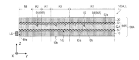
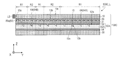
- FIG. 1 is a cross-sectional view schematically showing the light emitting device 100A_L.
- the light emitting device 100A_L includes a light source LS and a light guide member 100A.
- the light source LS is, for example, an LED device.
- a plurality of LED devices may be used as the light source LS.
- a plurality of LED devices are arranged, for example, in the X direction.
- the light guide member 100A is sheet-like having a first principal surface and a second principal surface opposite to the first principal surface.
- the main surface on the lower side is the first main surface
- the main surface on the upper side is the second main surface.
- sheet-like includes plate-like and film-like forms, regardless of the rigidity (flexibility) and thickness of the sheet.
- a sheet-like light guide member can be used in various forms such as a roll shape.
- the light guide member 100A receives the light emitted from the light source LS, propagates the light in the Y direction, and emits the light in the -Z direction. Therefore, the first main surface of the light guide member 100A functions as a light exit surface.
- the light propagation direction has variations (distribution) from the Y direction
- the light emission direction also has variations (distribution) from the -Z direction.
- a coupling optical system for efficiently guiding the light emitted from the light source LS to the light guide member 100A may be provided between the light guide member 100A and the light source LS.
- the light guide member 100A has a light guide layer 10 and a light distribution control structure having a plurality of internal spaces IS.
- the light guide layer 10 includes a light receiving portion that receives light emitted from the light source LS, a third main surface 10b located on the first main surface side (that is, the light emission surface side), and a second main surface side (that is, the light emission surface side). and a fourth main surface 10c located on the opposite side to the surface side.
- the light receiving portion of the light guide layer 10 is a side surface (light receiving side surface) 10a of the light guide layer 10 on the light source LS side.
- the fourth main surface 10c of the light guide layer 10 is the light guide member 100A. It is the second main surface.
- a plurality of internal spaces IS of the light distribution control structure form an interface that directs part of the light propagating in the light guide layer 10 toward the first main surface by total internal reflection (TIR).
- Each internal space IS has a first inclined surface ISa that directs part of the light propagating in the light guide layer 10 toward the first principal surface by total internal reflection, and a second inclined surface ISa opposite to the first inclined surface ISa. and a surface ISb.
- the light distribution control structure having a plurality of internal spaces IS is formed in the direction conversion layer 60A provided on the third main surface 10b side of the light guide layer 10.
- the direction changing layer 60A is composed of a shaping film 62A having a fifth main surface 62a having a plurality of recesses 64, and an adhesive layer 52 arranged on the fifth main surface 62a side of the shaping film 62A. .
- the adhesive layer 52 is positioned between the shaping film 62A and the light guide layer 10, and the light guide layer 10 and the shaping film 62A are adhered by the adhesive layer 52.
- the adhesive layer 54 and the base material layer 30 are arranged in this order on the first main surface side of the direction changing layer 60A, and the adhesive layer 54 forms the shaping film 62A and the base material layer 30. and are glued together.
- the light guide layer 10 and the substrate layer 30 may be transparent substrates or films. Preferred configurations of the light guide layer 10, base layer 30, shaped film 62A, and adhesive layers 52 and 54 will be described later.
- the light emitting device 100A_L has a region (hereinafter referred to as "first region”) R1 in which the light distribution control structure exists and a region (hereinafter referred to as "second region”) R2 in which the light distribution control structure does not exist.
- the first region R1 and the second region R2 are arranged so as to define a predetermined pattern when viewed from above in the direction normal to the first main surface.
- the "design” includes characters, numbers, symbols, pictures, patterns, combinations thereof, and the like.
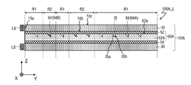
- FIG. 2 shows an example of arrangement of the first region R1 and the second region R2.
- FIG. 2 shows a state in which the light emitting device 100A_L is lit.
- the first region R1 in which the light distribution control structure exists is a region (light emitting region) that emits light in the lighting state
- the second region R2 in which the light distribution control structure does not exist substantially It is a region (non-light-emitting region) that does not emit light at all.
- the pattern defined by the first area R1 and the second area R2 is not limited to the one illustrated in FIG.
- the first region R1 and the second region R2 are separated by whether or not the recesses 64 of the shaping film 62A are filled with the adhesive layer 52.
- the plurality of recesses 64 of the shaping film 62A are located in the first region R1, and the plurality of first recesses 64A that are not filled with the adhesive layer 52 and the second region R2. and a plurality of second recesses 64B located and substantially filled by the adhesive layer 52 .
- the plurality of internal spaces IS are defined by the plurality of first recesses 64A of the shaping film 62A and the adhesive layer 52. That is, the region where the first concave portion 64A is located and not filled with the adhesive layer 52 becomes the first region R1 where the light distribution control structure exists. On the other hand, the region where the second concave portion 64B substantially filled with the adhesive layer 52 is located becomes the second region R2 that does not function as the light distribution control structure (that is, the light distribution control structure does not exist).
- the internal space IS is typically a gap (air cavity) filled with air.
- a light distribution structure described in International Publication No. 2019/087118 can be used. The entire disclosure of WO2019/087118 is incorporated herein by reference.
- the visible light transmittance and haze value of the light guide member 100A can be controlled.
- the visible light transmittance of the light guide member 100A is, for example, 60% or more, preferably 80% or more.
- the haze value of the light guide member 100A is, for example, less than 30%, preferably less than 10%.
- light with a wavelength of 380 nm or more and 780 nm or less is defined as visible light.
- Visible light transmittance and haze value can be measured using, for example, a haze meter (manufactured by Murakami Color Research Laboratory: trade name HM-150).
- the visible light transmittance of the light guide member 100A is preferably 60% or more, and the haze value of the light guide member 100A is 30%. % is preferred.
- the ratio of the area of the plurality of internal spaces IS to the area of the first region R1 is 1% or more and 80% or less. and more preferably 1% or more and 50% or less. From the viewpoint of obtaining a low haze value, the occupied area ratio of the internal space IS is preferably 30% or less, more preferably 10% or less.
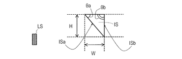
- FIG. 3 is a plan view schematically showing the light emitting device 100A_L.
- FIG. 4 is a cross-sectional view schematically showing the internal space IS, and
- FIG. 5 is a plan view schematically showing the internal space IS.
- the plurality of internal spaces IS can be arranged discretely in, for example, the light guide direction (Y direction) of the light guide layer 10 and a direction crossing the light guide direction.
- the discrete arrangement may or may not have periodicity (regularity) in at least one direction.
- the plurality of internal spaces IS be uniformly arranged in the first region R1.
- a plurality of internal spaces IS having substantially the same shape and convex curved surfaces in the same direction are arranged in the light guide direction (Y direction) of the light guide plate 10 and perpendicular to the light guide direction. are arranged discretely and periodically in the direction (X direction).
- the pitch Px of the internal spaces IS in the X direction is preferably 10 ⁇ m or more and 500 ⁇ m or less
- the pitch Py of the internal spaces IS in the Y direction is preferably 10 ⁇ m or more and 500 ⁇ m or less.
- an internal space IS is further provided which is arranged with a half pitch in each of the Y and X directions.
- the first inclined surface ISa forms a convex curved surface toward the light source LS when viewed from above in the direction normal to the first main surface of the light guide member 100A.
- the light source LS When a plurality of LED devices arranged in the X direction are used as the light source LS, the light emitted from each LED device spreads in the Y direction.
- the first inclined surface ISa having a curved surface acts more uniformly on light. Note that when a coupling optical system is provided between the light source LS and the light receiving side surface 10a of the light guide layer 10 so that highly parallel light (light with a small spread in the Y direction) is incident, the first inclined surface ISa may be parallel to the X direction.
- the discrete internal spaces IS for example, internal spaces such as grooves (for example, triangular prisms) extending in the X direction may be used.
- the cross-sectional shape of the internal space IS (the shape of the cross section perpendicular to the X direction and parallel to the YZ plane in FIG. 1) is, for example, the first main surface side of the light guide member 100A (- Z direction) is a triangle with an apex angle.
- the inclination angle ⁇ a of the first inclined surface ISa on the light source LS side is, for example, 10° or more and 70° or less. If the angle of inclination ⁇ a is less than 10°, the controllability of the light distribution may deteriorate, and the light extraction efficiency may also deteriorate. On the other hand, if the inclination angle ⁇ a exceeds 70°, it may become difficult to process the shaped film, for example.
- the inclination angle ⁇ b of the second inclined surface ISb is, for example, 50° or more and 100° or less. If the tilt angle ⁇ b is less than 50°, stray light may occur in an unintended direction. On the other hand, if the inclination angle ⁇ b exceeds 100°, it may become difficult to process the shaped film, for example.
- the cross-sectional shape of the internal space IS is not limited to the triangular shape illustrated here, and may be trapezoidal or the like.
- the two-dimensional size of the internal space IS is defined by the length L and width W of the internal space IS.
- the length L of the internal space IS is preferably 10 ⁇ m or more and 500 ⁇ m or less, for example.
- the width W of the internal space IS is preferably 1 ⁇ m or more and 100 ⁇ m or less, for example.
- the length L of the internal space IS is, for example, twice or more the width W of the internal space IS.
- the height H (see FIG. 4) of the internal space IS is preferably, for example, 1 ⁇ m or more and 100 ⁇ m or less from the viewpoint of light extraction efficiency.
- the first region R1 in which the light distribution control structure exists and the second region R2 in which the light distribution control structure does not exist are arranged so as to define a predetermined pattern.
- light can be emitted in a predetermined pattern. Therefore, illumination (light emission) rich in design and entertainment can be realized.
- the light emitting device 100A_L of the present embodiment has a light distribution control structure having a plurality of internal spaces IS (that is, using total internal reflection), it achieves high transparency (visible light transmittance). be able to.
- the light guide member 100A of the light emitting device 100A_L can have a visible light transmittance of, for example, 60% or more (preferably 80% or more).
- the sheet-shaped light-emitting device 100A_L is preferably used as an in-vehicle light-emitting device by being attached to the window glass of an automobile. Further, since the light-emitting device 100A_L having the above-described structure can have flexibility, it can be attached to curved glass. Therefore, the light emitting device 100A_L can be arranged on the front windshield or the rear windshield, which are large-area curved glass. A window glass may be used as part of the light emitting device 100A_L (the light guide layer 10 and the base material layer 30). Further, the light-emitting device 100A_L is not limited to vehicle-mounted applications, and can also be used for show windows and the like.
- a light distribution control structure having a plurality of internal spaces IS may be formed in the light guide layer 10 .
- the light distribution control structure having a plurality of internal spaces IS in the direction conversion layer 60A, high transparency in the off state, high light utilization efficiency in the on state, and high reliability , it is easy to realize high directivity to one side.
- the internal space IS in the light guide layer 10 When forming the internal space IS in the light guide layer 10, for example, as will be described later, it is conceivable to form a fine pattern (recess) defining the internal space IS in the film by laser processing. It may be difficult to form an anisotropic shape suitable for . If the anisotropic shape is not suitable, the irregular interface may reflect outside light (environmental light) in different directions, resulting in poor transparency in the off state. Moreover, the directivity in the lighting state is also lowered, and there is a possibility that the light utilization efficiency is lowered. Furthermore, even if a suitable anisotropic shape can be formed, the portion around the recess may be degraded due to the uneven energy of the laser beam.
- the light guide layer 10 can be made of a known material with high visible light transmittance.
- the light guide layer 10 is made of, for example, an acrylic resin such as polymethyl methacrylate (PMMA), a polycarbonate (PC) resin, a cycloolefin resin, or glass (for example, quartz glass, alkali-free glass, or borosilicate glass). be.
- the refractive index n GP of the light guide layer 10 is, for example, 1.40 or more and 1.80 or less. Unless otherwise specified, the refractive index refers to the refractive index measured with an ellipsometer at a wavelength of 550 nm.
- the thickness of the light guide layer 10 can be appropriately set according to the application.
- the thickness of the light guide layer 10 is, for example, 0.05 mm or more and 50 mm or less.
- the thickness of the base material layer 30 is, for example, 1 ⁇ m or more and 1000 ⁇ m or less, preferably 10 ⁇ m or more and 100 ⁇ m or less, and more preferably 20 ⁇ m or more and 80 ⁇ m or less.
- the refractive index of the base material layer 30 is preferably 1.40 or more and 1.70 or less, more preferably 1.43 or more and 1.65 or less.
- the shaping film 62A for forming the internal space IS can be produced, for example, by the method described in JP-T-2013-524288. Specifically, for example, the surface of a polymethyl methacrylate (PMMA) film is coated with a lacquer (for example, Fine Cure RM-64 manufactured by Sanyo Chemical Industries, Ltd.), and an optical pattern is embossed on the film surface containing the lacquer. , and then curing the lacquer to form the shaped film 62A.
- PMMA polymethyl methacrylate
- a lacquer for example, Fine Cure RM-64 manufactured by Sanyo Chemical Industries, Ltd.
- the thicknesses of the adhesive layers 52 and 54 are each independently, for example, 0.1 ⁇ m or more and 100 ⁇ m or less, preferably 0.3 ⁇ m or more and 100 ⁇ m or less, and more preferably 0.5 ⁇ m or more and 50 ⁇ m or less.
- the refractive indices of the adhesive layers 52 and 54 are each independently preferably 1.42 or more and 1.60 or less, more preferably 1.47 or more and 1.58 or less.
- the refractive index of the adhesive layers 52 and 54 is preferably close to the refractive index of the light guide layer 10, the base layer 30, or the shaping film 62A with which they are in contact, and the absolute value of the difference in refractive index is 0.2. The following are preferable.
- adhesive is used to include pressure-sensitive adhesives (also called adhesives).
- adhesives include rubber-based adhesives, acrylic-based adhesives, silicone-based adhesives, epoxy-based adhesives, cellulose-based adhesives, and polyester-based adhesives. These adhesives may be used alone or in combination of two or more.
- the adhesive layer 52 can adhere without filling the first concave portions 64A on the surface of the shaping film 62A.
- the adhesive described in International Publication No. 2021/167090, International Publication No. 2021/167091, or International Application PCT/JP2022/004554 by the present applicant is preferably used. be able to. The entire disclosure of these applications is incorporated herein by reference.
- the polyester-based adhesive described in International Application PCT/JP2022/004554 is preferred.
- the light guide layer 10 and the shaping film 62A must be combined.
- a laminating machine through the adhesive layer 52, if a mask having a mask pattern (opening corresponding to the first region R1) corresponding to the arrangement of the first region R1 and the second region R2 is used good.
- Various conditions such as the nip pressure of the laminating machine) during lamination can be appropriately set according to the specifications of the adhesive used, the size of the concave portion 64, and the like.
- the second concave portion 64B of the shaping film 62A does not necessarily have to be completely filled with the adhesive layer 52, and may be substantially filled to the extent that it does not function as a light distribution control structure.
- the second recess 64B of the shaping film 62A is filled with the adhesive layer 52 for bonding the light guide layer 10 and the shaping film 62A together. may be substantially filled with some material other than the adhesive layer 52 so as not to function as a light distribution control structure.
- the refractive index of the material filling the second recesses 64B is preferably close to the refractive index of the shaping film 62A, and the absolute value of the difference in refractive index is preferably 0.2 or less.
- the light guide layer 10 and the shaping film 62A are formed.
- some material for example, an adhesive
- the light guide layer 10 and the shaping film 62A can be laminated to obtain a configuration in which the first concave portions 64A and the second concave portions 64B are mixed. can.
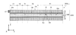
- FIG. 1 shows an example in which a light distribution control structure is formed in the direction changing layer 60A provided on the third main surface 10b side of the light guide layer 10, but as shown in FIG.
- a light distribution control structure may be formed in the direction changing layer 60A' provided on the fourth main surface 10c side of the 10 .
- the direction changing layer 60A' is composed of a shaping film 62A having a fifth main surface 62a having a plurality of recesses 64, and an adhesive layer 52 arranged on the fifth main surface 62a side of the shaping film 62A.
- the substrate layer 30 is arranged on the opposite side of the adhesive layer 52 to the shaping film 62A, and the shaping film 62A and the substrate layer 30 are adhered by the adhesive layer 52 . Further, the light guide layer 10 and the shaped film 62A are adhered by the adhesive layer 54 arranged on the fourth main surface 10c side of the light guide layer 10 .
- the third main surface 10b of the light guide layer 10 is the light guide member 100A. It is a 1st main surface.
- the end surface of the base material layer 30 (the end surface located on the same side as the light receiving side surface 10a of the light guide layer 10)
- a further light source LS' may be provided which emits light towards ).
- the base material layer 30 functions as a further light guide layer.
- FIG. 8 is a cross-sectional view schematically showing the light emitting device 100B_L. The following description will focus on the differences between the light emitting device 100B_L of the present embodiment and the light emitting device 100A_L of the first embodiment.
- the light guide member 100B included in the light emitting device 100B_L has a light distribution control structure having a plurality of internal spaces IS, similar to the light guide member 100A of the light emitting device 100A_L.
- a light distribution control structure having a plurality of internal spaces IS is formed in the direction changing layer 60B provided on the third main surface 10b side of the light guide layer 10 .
- the direction changing layer 60B is composed of a shaped film 62B having a fifth main surface 62a with a plurality of recesses 64, and an adhesive layer 52 arranged on the fifth main surface 62a side of the shaped film 62B. .
- the light emitting device 100B_L has a first region R1 in which the light distribution control structure exists and a second region R2 in which the light distribution control structure does not exist.
- the first region R1 and the second region R2 are arranged so as to define a predetermined pattern when viewed from above in the direction normal to the first main surface.
- the first region R1 and the second region R2 are divided depending on whether or not the recesses 64 of the shaping film 62B are formed. As shown in FIG. 8, the plurality of recesses 64 of the shaping film 62B are formed only in the first region R1 of the first region R1 and the second region R2 (that is, selectively in the first region R1). there is
- a plurality of internal spaces IS are defined by a plurality of recesses 64 of the shaping film 62B and the adhesive layer 52. Therefore, the region where the concave portion 64 exists is the first region R1 where the light distribution control structure exists. On the other hand, the region where the concave portion 64 does not exist becomes the second region R2 that does not function as the light distribution control structure (that is, the light distribution control structure does not exist).
- the light emitting device 100B_L of the present embodiment can also emit light in a predetermined pattern and achieve high transparency (visible light transmittance).
- FIG. 9 is a cross-sectional view schematically showing the light emitting device 100C_L. The following description focuses on the differences between the light emitting device 100C_L of the present embodiment and the light emitting device 100A_L of the first embodiment.
- the light guide member 100C included in the light emitting device 100C_L has a light distribution control structure having a plurality of internal spaces IS, similar to the light guide member 100A of the light emitting device 100A_L.
- a light distribution control structure having a plurality of internal spaces IS is formed in the direction changing layer 60A provided on the third main surface 10b side of the light guide layer 10 .
- the direction changing layer 60A has the same configuration as the direction changing layer 60A of the light emitting device 100A_L of the first embodiment.
- the light guide member 100C further has a light coupling layer 80 provided between the light guide layer 10 and the direction changing layer 60A.
- the optical coupling layer 80 has a plurality of low refractive index regions 80 a having a refractive index n C smaller than the refractive index n GP of the light guide layer 10 .
- Each low refractive index region 80a is formed in a dot shape with a size of 1 ⁇ m or more and 1000 ⁇ m or less, for example.
- the optical coupling layer 80 having a plurality of low refractive index regions 80 a is supported by the base material layer 31 , and the light guide layer 10 and the base material layer 31 are adhered by the adhesive layer 56 . Further, the base material layer 31 and the shaping film 62A of the direction changing layer 60A are adhered by an adhesive layer 52. As shown in FIG.
- the optical coupling layer 80 having a plurality of low refractive index regions 80a is provided, so that the light propagating through the light guide layer 10 is more selectively and efficiently directed to the direction changing layer 60A.
- the arrangement density of the plurality of low refractive index regions 80a it is possible to control the uniformity of the light emitted from the first region R1.
- the uniformity of light can be improved by arranging the low refractive index regions 80a densely on the light source LS side and sparsely spaced away from the light source LS.
- the refractive index n C of the low refractive index region 80a is preferably from 1.05 to 1.30, more preferably from 1.05 to 1.25.
- the difference between the refractive index nGP of the light guide layer 10 and the refractive index nC of the low refractive index region 80a is preferably 0.20 or more, more preferably 0.23 or more, and still more preferably 0.25. That's it.
- the low refractive index region 80a having a refractive index n C of 1.30 or less can be, for example, a porous region having a void structure inside.
- the thickness of the low refractive index region 80a is, for example, 0.3 ⁇ m or more and 5 ⁇ m or less.
- the low refractive index region 80a When the low refractive index region 80a is a porous region, its porosity is preferably 35% by volume or more, more preferably 38% by volume or more, and particularly preferably 40% by volume or more. Within such a range, the low refractive index region 80a having a particularly low refractive index can be formed.
- the upper limit of the porosity is, for example, 90% by volume or less, preferably 75% by volume or less. Within such a range, the low refractive index region 80a having excellent strength can be obtained.
- the porosity is calculated by Lorentz-Lorenz's formula from refractive index values measured by an ellipsometer.
- the low refractive index region 80a for example, a low refractive index layer having a void structure disclosed in WO2019/146628 can be used.
- the entire disclosure of WO2019/146628 is incorporated herein by reference.
- the low refractive index regions 80a having a void structure are composed of substantially spherical particles such as silica particles, silica particles having micropores, hollow silica nanoparticles, fibrous particles such as cellulose nanofibers, alumina nanofibers, silica nanofibers, and the like. It may include particles, tabular particles such as nanoclays composed of bentonite, and the like.
- the low refractive index region 80a having a void structure can be a porous body configured by directly chemically bonding particles (for example, microporous particles) to each other. At least a part of the particles forming the low refractive index region 80a having a void structure may be bonded together via a small amount (for example, the mass of the particles or less) of one component of the binder.
- the porosity and refractive index n C of the low refractive index region 80a can be adjusted by the particle size, particle size distribution, etc. of the particles forming the low refractive index region 80a.
- Methods for obtaining the low refractive index region 80a having a void structure include, for example, JP-A-2010-189212, JP-A-2008-040171, JP-A-2006-011175, International Publication No. 2004/113966, and Methods described in those references are included. All of the disclosures of JP-A-2010-189212, JP-A-2008-040171, JP-A-2006-011175, and International Publication No. 2004/113966 are incorporated herein by reference.
- a silica porous body can be suitably used as the low refractive index region 80a having a void structure.
- a silica porous body is produced, for example, by the following method. a silicon compound; hydrolyzable silanes and/or silsesquioxane, and a method of hydrolyzing and polycondensing at least one of its partial hydrolyzate and dehydration condensate; porous particles and/or hollow fine particles; method, method of generating an airgel layer using the springback phenomenon, pulverizing the gel-like silicon compound obtained by the sol-gel method, and chemically pulverizing the resulting pulverized microporous particles with a catalyst or the like. and a method using a combined pulverized gel.
- the low refractive index region 80a is not limited to the silica porous body, nor is the manufacturing method limited to the exemplified manufacturing method, and may be manufactured by any manufacturing method.
- Silsesquioxane is a silicon compound having (RSiO 1.5 , R is a hydrocarbon group) as a basic structural unit, and is strictly different from silica having SiO 2 as a basic structural unit.
- a porous material containing silsesquioxane as a basic structural unit is also referred to herein as a silica porous material or a silica-based porous material, since it has a network structure crosslinked with silica in common.
- the silica porous body can be composed of microporous particles of a gel-like silicon compound bonded together.
- pulverized bodies of the gelled silicon compound can be mentioned.
- the silica porous body can be formed, for example, by coating a base material with a coating liquid containing a pulverized gel-like silicon compound.
- the pulverized gel-like silicon compound can be chemically bonded (for example, siloxane bond) by the action of a catalyst, light irradiation, heating, or the like.
- FIG. 10 is a cross-sectional view schematically showing the light emitting device 100D_L. The following description focuses on the differences between the light emitting device 100D_L of the present embodiment and the light emitting device 100C_L of the third embodiment.
- the light guide member 100D included in the light emitting device 100D_L has a light distribution control structure with a plurality of internal spaces IS.
- a light distribution control structure having a plurality of internal spaces IS is formed in a direction changing layer 60C provided on the third main surface 10b side of the light guide layer 10.
- the direction changing layer 60C is composed of a shaping film 62A having a fifth main surface 62a having a plurality of recesses 64, and an adhesive layer 52 arranged on the fifth main surface 62a side of the shaping film 62A. .
- the plurality of recesses 64 of the shaped film 62A are formed substantially entirely on the light guide member 100D in plan view, and are not filled with the adhesive layer 52. Therefore, the plurality of internal spaces IS are provided in substantially the entirety of the light guide member 100D in plan view.
- the light guide member 100D further has a light coupling layer 80 provided between the light guide layer 10 and the direction changing layer 60C.
- the optical coupling layer 80 has a plurality of low refractive index regions 80 a having a refractive index n C smaller than the refractive index n GP of the light guide layer 10 .
- the light emitting device 100D_L of the present embodiment includes a region R1′ where the optical coupling layer 80 exists (hereinafter referred to as “first region”) and a region R2 where the optical coupling layer 80 does not exist (hereinafter referred to as “second region”). ' and The first region R1' and the second region R2' are arranged so as to define a predetermined pattern when viewed from above in the direction normal to the first main surface. Although not shown here, the first region R1' and the second region R2' can be arranged in the same manner as the first region R1 and the second region R2 shown in FIG.
- the first region R1' in which the optical coupling layer 80 exists is a region (low-luminance light-emitting region) that emits light (or substantially does not emit light) with relatively low luminance in the lighting state.
- the second region R2' in which the optical coupling layer 80 does not exist is a region that emits light with relatively high luminance in the lighting state (high luminance light emitting region).
- each low refractive index region 80a is a porous region 81 having a void structure inside. It is classified according to whether or not As shown in FIG. 10, the plurality of porous regions 81 are formed only in the first region R1' (that is, selectively in the first region R1') of the first region R1' and the second region R2'. ing. As already described, the plurality of low refractive index regions 80a are a plurality of porous regions 81 having a void structure inside (that is, defined by a plurality of porous regions 81), so the porous regions 81 exist.
- the region where the optical coupling layer 80 exists is the first region R1′ where the optical coupling layer 80 exists, and the region where the porous region 81 does not exist becomes the second region R2′ where the optical coupling layer 80 does not exist.
- the first region R1′ in which the optical coupling layer 80 exists and the second region R2′ in which the optical coupling layer 80 does not exist define a predetermined pattern.
- the predetermined pattern By being arranged in the position, it is possible to emit light so that a predetermined pattern can be visually recognized. Therefore, illumination (light emission) rich in design and entertainment can be realized.
- the light emitting device 100D_L of the present embodiment has a light distribution control structure having a plurality of internal spaces IS (that is, using total internal reflection), it achieves high transparency (visible light transmittance). be able to. Further, the sheet-shaped light emitting device 100D_L is suitably used as a vehicle-mounted light emitting device.
- a coating method or a printing method can be preferably used.
- a coating method a mask having a predetermined pattern may be used for coating.
- a plate-type printing method such as gravure printing may be used, or a plateless printing method such as inkjet printing may be used.
- FIG. 11 is a cross-sectional view schematically showing the light emitting device 100E_L. The following description will focus on the differences between the light emitting device 100E_L of the present embodiment and the light emitting device 100D_L of the fourth embodiment.
- the light guide member 100E included in the light emitting device 100E_L has a light distribution control structure with a plurality of internal spaces IS.
- a light distribution control structure having a plurality of internal spaces IS is formed in a direction changing layer 60C provided on the third main surface 10b side of the light guide layer 10.
- This direction changing layer 60C has the same configuration as the direction changing layer 60C of the light emitting device 100D_L of the fourth embodiment.
- the light guide member 100E further has an optical coupling layer 80 provided between the light guide layer 10 and the direction changing layer 60C.
- the optical coupling layer 80 has a plurality of low refractive index regions 80 a having a refractive index n C smaller than the refractive index n GP of the light guide layer 10 .
- the multiple low refractive index regions 80a are multiple porous regions 81 having void structures therein.
- the light emitting device 100E_L of the present embodiment also has a first region R1' in which the optical coupling layer 80 exists and a second region R2' in which the optical coupling layer 80 does not exist.
- the first region R1' and the second region R2' are arranged so as to define a predetermined pattern when viewed from above in the direction normal to the first main surface.
- the first region R1′ and the second region R2′ are defined by whether or not the void structure of the porous regions 81 is filled with the adhesive layer 56 provided so as to be in contact with the plurality of porous regions 81. or As shown in FIG. 11, the plurality of porous regions 81 are located within the first region R1′, and the plurality of first porous regions 81A in which the void structure is not filled with the adhesive layer 56 and the second region a plurality of second porous regions 81B located within R2′ and having void structures substantially filled by adhesive layer 56;
- the region where the second porous region 81B in which the void structure is substantially filled with the adhesive layer 56 is arranged does not function as the optical coupling layer 80. That is, the plurality of low refractive index regions 80a are defined by the plurality of first porous regions 81A in which the void structure is not filled with the adhesive layer 56. As shown in FIG.
- the adhesive layer 56 those exemplified as adhesives suitable for forming the adhesive layer 52 can be used.
- the adhesive layer 56 not to fill the void structure of the first porous region 81A of the plurality of porous regions 81 and substantially fill the void structure of the second porous region 81B, for example, a plurality of
- the arrangement of the first region R1' and the second region R2' A mask having a corresponding mask pattern (opening corresponding to the first region R1') may be used.
- Various conditions (such as the nip pressure of the laminating machine) during lamination can be appropriately set according to the specifications of the adhesive used, the material of the porous region 81, and the like.
- the void structure of the second porous region 81B does not necessarily have to be completely filled with the adhesive layer 56 as long as it does not function as the optical coupling layer 80 substantially. Moreover, even when the void structure of the second porous region 81B is completely filled with the adhesive layer 56, the refractive index of the second porous region 81B and the refractive index of the adhesive layer 56 are completely different. may not match.
- the difference between the refractive index of the second porous region 81B and the refractive index of the adhesive layer 56 is preferably 0.3 or less, more preferably 0.2 or less.
- the light emitting device 100E_L of the present embodiment can also emit light in a predetermined pattern and achieve high transparency (visible light transmittance).
- the configuration in which the void structure of the second porous region 81B is filled with the adhesive layer 56 has been described, but the second porous region 81B is adhered so as not to function as the optical coupling layer 80. It may be substantially filled with some material other than the agent layer 56 . In that case, after selectively filling the pore structure of a part of the porous regions 81 (the porous regions 81 that become the second porous regions 81B) of the plurality of porous regions 81 with some material, the plurality of porous regions 81 are formed.
- the laminated structure and the light guide layer 10 may be laminated by, for example, bonding the laminated structure including the base layer 31 and the base material layer 31 to the light guide layer 10 via the adhesive layer 56 .
- the material that fills the void structure of the second porous region 81B is preferably a material in which the difference between the refractive index of the second porous region 81B and the refractive index of the adhesive layer 56 is 0.3 or less. .2 or less is more preferable.
- FIG. 12 is a cross-sectional view schematically showing the light emitting device 100F_L. The following description focuses on the differences between the light emitting device 100F_L of the present embodiment and the light emitting device 100A_L of the first embodiment.
- the light guide member 100F included in the light emitting device 100F_L is configured such that the thickness of the light guide layer 10W and the base material layer 30W increases as the distance from the light receiving side surface 10a (that is, from the light source LS) increases. It differs from the light guide member 100A of the light emitting device 100A_L in that That is, the light guide layer 10W and the base material layer 30W of the light guide member 100F are each formed in a wedge shape.
- the light guide layer 10W which is configured such that the thickness increases as the distance from the light receiving side surface 10a increases, the light guide layer 10W is configured to have a uniform thickness, and the light guide layer 10W is configured to have a constant thickness.
- the angle formed by the light traveling toward the fourth main surface 10c while propagating toward the fourth main surface 10c and the fourth main surface 10c becomes smaller (that is, the angle of incidence on the fourth main surface 10c becomes larger). Less light (stray light). Therefore, directivity to one side is improved.
- the wedge-shaped base layer 30W may have a thickness similar to that of the wedge-shaped light guide layer 10W.
- the light emitting device 100A_L of Embodiment 1 may be modified in the same manner as the modified example described with reference to FIG. That is, as shown in FIG. 13, the light distribution control structure may be formed in the direction changing layer 60A' provided on the fourth main surface 10c side of the light guide layer 10W.
- a further light source may be provided that emits light toward the end face (the end face located on the same side as the light receiving side surface 10a of the light guide layer 10W).
- the base material layer 30W functions as a further light guide layer.
- one of the light guide layer 10W and the base layer 30W may be replaced with a non-wedge-shaped one.
- a wedge-shaped light guide layer 10W and/or a base layer 30W are used instead of the light guide layer 10 and/or the base layer 30 of the light emitting devices 100B_L, 100C_L, 100D_L, and 100E_L of Embodiments 2 to 5, a wedge-shaped light guide layer 10W and/or a base layer 30W are used. good too.
- a light distribution control structure having a space IS may be formed in the light guide layer.
- Such a light guide layer is formed, for example, by laminating a first film having no pattern and a second film having a desired fine pattern formed thereon, or using an adhesive (pressure-sensitive adhesive). including).
- Laser patterning, direct laser imaging, laser drilling, masked or maskless laser or electron beam irradiation are used to form the micropattern on the second film.
- individual characteristics may be imparted by printing, inkjet printing, screen printing, or the like to change the material or the refractive index value.
- Micro/nanodispensing, dosing, direct "writing”, discrete laser sintering, micro electrical discharge machining (micro EDM) or micromachining, micromolding, imprinting, embossing and the like can also be used.
- Antireflection layer, antiglare layer and hard coat layer Light-emitting devices according to embodiments of the present invention are not limited to the examples described above, and may be modified in various ways.
- an antireflection layer, an antiglare layer and/or a hard coat layer (for example, a pencil hardness of H or higher) may be provided instead of the base layer 30 of the light emitting device 100A_L, etc.
- an antireflection layer, an antiglare layer and/or a hard coat layer may be provided on the substrate layer 30 .
- An antireflection layer, an antiglare layer and/or a hard coat layer may be provided on the side of the light guide layer 10 opposite to the base layer 30 side.
- the antireflection layer, antiglare layer and hard coat layer can be formed by known methods using known materials.
- the sheet-like transparent light-emitting device described above is used for building members.
- the light-emitting device itself can be used as a building member, or can be used as a part of the building member.
- Building members include those for exteriors and those for interiors.
- it can be used as a window member, a wall member, a partition, a ceiling (skylight) member, a stair member, a handrail member, and a floor member.
- it can be used as a light-emitting device (lighting device) for street use, crime prevention use, emergency use, garden use, pool/pond (underwater), warehouse, factory, and under the eaves (outdoors). Both are used as transparent plates when not in use.
- a light emitting device capable of emitting light in a predetermined pattern and having sufficiently high transparency and a light guide member for a light emitting device suitably used for such a light emitting device are provided.
- a light-emitting device according to an embodiment of the present invention is suitably used for in-vehicle use.
Landscapes
- Physics & Mathematics (AREA)
- General Physics & Mathematics (AREA)
- Optics & Photonics (AREA)
- Engineering & Computer Science (AREA)
- General Engineering & Computer Science (AREA)
- Planar Illumination Modules (AREA)
Priority Applications (5)
| Application Number | Priority Date | Filing Date | Title |
|---|---|---|---|
| JP2023531791A JPWO2023276704A1 (https=) | 2021-06-29 | 2022-06-16 | |
| KR1020237036870A KR20240026886A (ko) | 2021-06-29 | 2022-06-16 | 발광 장치용 도광부재 및 발광 장치 |
| EP22832854.8A EP4365481A4 (en) | 2021-06-29 | 2022-06-16 | LIGHT GUIDE ELEMENT FOR LIGHT EMITTING DEVICE AND LIGHT EMITTING DEVICE |
| US18/288,433 US20240230978A1 (en) | 2021-06-29 | 2022-06-16 | Light guide member for light emission device and light emission device |
| CN202280032264.8A CN117396940A (zh) | 2021-06-29 | 2022-06-16 | 发光装置用导光部件以及发光装置 |
Applications Claiming Priority (2)
| Application Number | Priority Date | Filing Date | Title |
|---|---|---|---|
| JP2021107331 | 2021-06-29 | ||
| JP2021-107331 | 2021-06-29 |
Publications (1)
| Publication Number | Publication Date |
|---|---|
| WO2023276704A1 true WO2023276704A1 (ja) | 2023-01-05 |
Family
ID=84692344
Family Applications (1)
| Application Number | Title | Priority Date | Filing Date |
|---|---|---|---|
| PCT/JP2022/024179 Ceased WO2023276704A1 (ja) | 2021-06-29 | 2022-06-16 | 発光装置用導光部材および発光装置 |
Country Status (7)
| Country | Link |
|---|---|
| US (1) | US20240230978A1 (https=) |
| EP (1) | EP4365481A4 (https=) |
| JP (1) | JPWO2023276704A1 (https=) |
| KR (1) | KR20240026886A (https=) |
| CN (1) | CN117396940A (https=) |
| TW (1) | TW202314303A (https=) |
| WO (1) | WO2023276704A1 (https=) |
Cited By (2)
| Publication number | Priority date | Publication date | Assignee | Title |
|---|---|---|---|---|
| WO2025205370A1 (ja) * | 2024-03-29 | 2025-10-02 | 日東電工株式会社 | 照明装置 |
| WO2025205368A1 (ja) * | 2024-03-29 | 2025-10-02 | 日東電工株式会社 | 賦形フィルム、積層体、導光層付き積層体、及び照明装置 |
Citations (11)
| Publication number | Priority date | Publication date | Assignee | Title |
|---|---|---|---|---|
| JP2004069729A (ja) | 2002-08-01 | 2004-03-04 | Okaya Electric Ind Co Ltd | 光点式表示器 |
| JP2004113966A (ja) | 2002-09-27 | 2004-04-15 | Kurashiki Seni Kako Kk | 生分解性空気清浄用フィルター |
| JP2006011175A (ja) | 2004-06-28 | 2006-01-12 | Pentax Corp | 反射防止膜を有する光学素子及びその製造方法 |
| JP2008040171A (ja) | 2006-08-07 | 2008-02-21 | Pentax Corp | セルフクリーニング効果を有する反射防止膜を設けた光学素子及びその製造方法 |
| JP2010189212A (ja) | 2009-02-17 | 2010-09-02 | Shinshu Univ | 多孔質シリカ膜およびその製造方法 |
| JP2013524288A (ja) | 2010-04-06 | 2013-06-17 | モディリス ホールディングス エルエルシー | 内部空洞光学素子 |
| WO2019087118A1 (en) | 2017-11-01 | 2019-05-09 | Nitto Denko Corporation | Light distribution structure and element, related method and uses |
| WO2019146628A1 (ja) | 2018-01-26 | 2019-08-01 | 日東電工株式会社 | Led照明器具用フィルム、led照明器具 |
| JP2021002065A (ja) * | 2016-11-17 | 2021-01-07 | パナソニックIpマネジメント株式会社 | 表示装置 |
| WO2021167090A1 (ja) | 2020-02-21 | 2021-08-26 | 日東電工株式会社 | 接着剤層、積層体、光学積層体および光学積層体の製造方法、ならびに光学装置 |
| WO2021167091A1 (ja) | 2020-02-21 | 2021-08-26 | 日東電工株式会社 | 接着剤組成物層、積層体、光学積層体および光学装置、ならびに光学積層体の製造方法 |
Family Cites Families (13)
| Publication number | Priority date | Publication date | Assignee | Title |
|---|---|---|---|---|
| JP2002333618A (ja) * | 2001-05-07 | 2002-11-22 | Nitto Denko Corp | 反射型液晶表示装置 |
| JP4122161B2 (ja) * | 2002-02-04 | 2008-07-23 | 日本電産コパル株式会社 | 面発光装置 |
| WO2007083805A1 (ja) * | 2006-01-23 | 2007-07-26 | Fujifilm Corporation | 面状照明装置 |
| US7955531B1 (en) * | 2006-04-26 | 2011-06-07 | Rohm And Haas Electronic Materials Llc | Patterned light extraction sheet and method of making same |
| FR2908523B1 (fr) * | 2006-11-14 | 2011-04-01 | Saint Gobain | Structure diffusante plane, son procede de fabrication et ses applications. |
| JP4351696B2 (ja) * | 2006-12-01 | 2009-10-28 | アルプス電気株式会社 | 照光機構付きの入力装置 |
| JP4384214B2 (ja) * | 2007-09-27 | 2009-12-16 | 株式会社 日立ディスプレイズ | 面発光素子,画像表示素子及びそれを用いた画像表示装置 |
| KR20120115568A (ko) * | 2010-02-10 | 2012-10-18 | 쓰리엠 이노베이티브 프로퍼티즈 컴파니 | 점탄성 층을 구비한 조명 장치 |
| US8834004B2 (en) * | 2012-08-13 | 2014-09-16 | 3M Innovative Properties Company | Lighting devices with patterned printing of diffractive extraction features |
| RU2015117517A (ru) * | 2012-10-11 | 2016-12-10 | Конинклейке Филипс Н.В. | Тонкая и эффективная световодная система |
| WO2014199572A1 (ja) * | 2013-06-13 | 2014-12-18 | パナソニックIpマネジメント株式会社 | 光取り込みシートおよび光取り込みロッド、ならびにそれらを用いた受光装置、発光装置および光ファイバー用増幅器 |
| KR20170135954A (ko) * | 2015-04-10 | 2017-12-08 | 쓰리엠 이노베이티브 프로퍼티즈 캄파니 | 라미네이팅된 추출 필름을 포함하는 도광체 |
| KR102746689B1 (ko) * | 2018-05-21 | 2024-12-26 | 닛토덴코 가부시키가이샤 | 개량된 배광 소자 |
-
2022
- 2022-06-16 CN CN202280032264.8A patent/CN117396940A/zh active Pending
- 2022-06-16 KR KR1020237036870A patent/KR20240026886A/ko active Pending
- 2022-06-16 EP EP22832854.8A patent/EP4365481A4/en active Pending
- 2022-06-16 JP JP2023531791A patent/JPWO2023276704A1/ja active Pending
- 2022-06-16 US US18/288,433 patent/US20240230978A1/en active Pending
- 2022-06-16 WO PCT/JP2022/024179 patent/WO2023276704A1/ja not_active Ceased
- 2022-06-24 TW TW111123635A patent/TW202314303A/zh unknown
Patent Citations (11)
| Publication number | Priority date | Publication date | Assignee | Title |
|---|---|---|---|---|
| JP2004069729A (ja) | 2002-08-01 | 2004-03-04 | Okaya Electric Ind Co Ltd | 光点式表示器 |
| JP2004113966A (ja) | 2002-09-27 | 2004-04-15 | Kurashiki Seni Kako Kk | 生分解性空気清浄用フィルター |
| JP2006011175A (ja) | 2004-06-28 | 2006-01-12 | Pentax Corp | 反射防止膜を有する光学素子及びその製造方法 |
| JP2008040171A (ja) | 2006-08-07 | 2008-02-21 | Pentax Corp | セルフクリーニング効果を有する反射防止膜を設けた光学素子及びその製造方法 |
| JP2010189212A (ja) | 2009-02-17 | 2010-09-02 | Shinshu Univ | 多孔質シリカ膜およびその製造方法 |
| JP2013524288A (ja) | 2010-04-06 | 2013-06-17 | モディリス ホールディングス エルエルシー | 内部空洞光学素子 |
| JP2021002065A (ja) * | 2016-11-17 | 2021-01-07 | パナソニックIpマネジメント株式会社 | 表示装置 |
| WO2019087118A1 (en) | 2017-11-01 | 2019-05-09 | Nitto Denko Corporation | Light distribution structure and element, related method and uses |
| WO2019146628A1 (ja) | 2018-01-26 | 2019-08-01 | 日東電工株式会社 | Led照明器具用フィルム、led照明器具 |
| WO2021167090A1 (ja) | 2020-02-21 | 2021-08-26 | 日東電工株式会社 | 接着剤層、積層体、光学積層体および光学積層体の製造方法、ならびに光学装置 |
| WO2021167091A1 (ja) | 2020-02-21 | 2021-08-26 | 日東電工株式会社 | 接着剤組成物層、積層体、光学積層体および光学装置、ならびに光学積層体の製造方法 |
Non-Patent Citations (1)
| Title |
|---|
| See also references of EP4365481A4 |
Cited By (2)
| Publication number | Priority date | Publication date | Assignee | Title |
|---|---|---|---|---|
| WO2025205370A1 (ja) * | 2024-03-29 | 2025-10-02 | 日東電工株式会社 | 照明装置 |
| WO2025205368A1 (ja) * | 2024-03-29 | 2025-10-02 | 日東電工株式会社 | 賦形フィルム、積層体、導光層付き積層体、及び照明装置 |
Also Published As
| Publication number | Publication date |
|---|---|
| EP4365481A1 (en) | 2024-05-08 |
| US20240230978A1 (en) | 2024-07-11 |
| EP4365481A4 (en) | 2025-10-08 |
| KR20240026886A (ko) | 2024-02-29 |
| JPWO2023276704A1 (https=) | 2023-01-05 |
| CN117396940A (zh) | 2024-01-12 |
| TW202314303A (zh) | 2023-04-01 |
Similar Documents
| Publication | Publication Date | Title |
|---|---|---|
| CN111295606B (zh) | 光分布结构和元件,相关方法和用途 | |
| JP7328257B2 (ja) | 改良された配光素子 | |
| KR102814283B1 (ko) | 조명 장치용 도광부재, 조명 장치 및 건축부재 | |
| WO2023276704A1 (ja) | 発光装置用導光部材および発光装置 | |
| CN117501043A (zh) | 照明装置用导光部件以及照明装置 | |
| JP7462840B2 (ja) | 照明装置用導光部材および照明装置 | |
| WO2023276705A1 (ja) | 光学積層体および照明装置 | |
| WO2024070908A1 (ja) | 照明装置 | |
| WO2022244474A1 (ja) | 光学装置 | |
| WO2023276836A1 (ja) | 照明装置用導光部材および照明装置 | |
| JP2024174483A (ja) | 積層フィルム、およびロール | |
| WO2024070909A1 (ja) | 光学装置、光学部材および導光部材 | |
| WO2022260061A1 (ja) | 照明装置およびタスクライト | |
| JP2026071234A (ja) | 光学インカップリングテープ、これを用いたライトガイド、およびその製造方法 |
Legal Events
| Date | Code | Title | Description |
|---|---|---|---|
| 121 | Ep: the epo has been informed by wipo that ep was designated in this application |
Ref document number: 22832854 Country of ref document: EP Kind code of ref document: A1 |
|
| WWE | Wipo information: entry into national phase |
Ref document number: 2023531791 Country of ref document: JP |
|
| WWE | Wipo information: entry into national phase |
Ref document number: 18288433 Country of ref document: US |
|
| WWE | Wipo information: entry into national phase |
Ref document number: 202280032264.8 Country of ref document: CN |
|
| WWE | Wipo information: entry into national phase |
Ref document number: 2022832854 Country of ref document: EP |
|
| NENP | Non-entry into the national phase |
Ref country code: DE |
|
| ENP | Entry into the national phase |
Ref document number: 2022832854 Country of ref document: EP Effective date: 20240129 |