WO2023228473A1 - 炭化珪素半導体装置 - Google Patents
炭化珪素半導体装置 Download PDFInfo
- Publication number
- WO2023228473A1 WO2023228473A1 PCT/JP2023/002283 JP2023002283W WO2023228473A1 WO 2023228473 A1 WO2023228473 A1 WO 2023228473A1 JP 2023002283 W JP2023002283 W JP 2023002283W WO 2023228473 A1 WO2023228473 A1 WO 2023228473A1
- Authority
- WO
- WIPO (PCT)
- Prior art keywords
- region
- electric field
- main surface
- maximum value
- silicon carbide
- Prior art date
- Legal status (The legal status is an assumption and is not a legal conclusion. Google has not performed a legal analysis and makes no representation as to the accuracy of the status listed.)
- Ceased
Links
Images


Classifications
-
- H—ELECTRICITY
- H10—SEMICONDUCTOR DEVICES; ELECTRIC SOLID-STATE DEVICES NOT OTHERWISE PROVIDED FOR
- H10D—INORGANIC ELECTRIC SEMICONDUCTOR DEVICES
- H10D30/00—Field-effect transistors [FET]
- H10D30/60—Insulated-gate field-effect transistors [IGFET]
- H10D30/64—Double-diffused metal-oxide semiconductor [DMOS] FETs
- H10D30/66—Vertical DMOS [VDMOS] FETs
- H10D30/668—Vertical DMOS [VDMOS] FETs having trench gate electrodes, e.g. UMOS transistors
-
- H—ELECTRICITY
- H10—SEMICONDUCTOR DEVICES; ELECTRIC SOLID-STATE DEVICES NOT OTHERWISE PROVIDED FOR
- H10D—INORGANIC ELECTRIC SEMICONDUCTOR DEVICES
- H10D30/00—Field-effect transistors [FET]
- H10D30/01—Manufacture or treatment
- H10D30/021—Manufacture or treatment of FETs having insulated gates [IGFET]
- H10D30/028—Manufacture or treatment of FETs having insulated gates [IGFET] of double-diffused metal oxide semiconductor [DMOS] FETs
- H10D30/0291—Manufacture or treatment of FETs having insulated gates [IGFET] of double-diffused metal oxide semiconductor [DMOS] FETs of vertical DMOS [VDMOS] FETs
- H10D30/0297—Manufacture or treatment of FETs having insulated gates [IGFET] of double-diffused metal oxide semiconductor [DMOS] FETs of vertical DMOS [VDMOS] FETs using recessing of the gate electrodes, e.g. to form trench gate electrodes
-
- H—ELECTRICITY
- H10—SEMICONDUCTOR DEVICES; ELECTRIC SOLID-STATE DEVICES NOT OTHERWISE PROVIDED FOR
- H10D—INORGANIC ELECTRIC SEMICONDUCTOR DEVICES
- H10D62/00—Semiconductor bodies, or regions thereof, of devices having potential barriers
- H10D62/10—Shapes, relative sizes or dispositions of the regions of the semiconductor bodies; Shapes of the semiconductor bodies
- H10D62/102—Constructional design considerations for preventing surface leakage or controlling electric field concentration
- H10D62/103—Constructional design considerations for preventing surface leakage or controlling electric field concentration for increasing or controlling the breakdown voltage of reverse-biased devices
- H10D62/105—Constructional design considerations for preventing surface leakage or controlling electric field concentration for increasing or controlling the breakdown voltage of reverse-biased devices by having particular doping profiles, shapes or arrangements of PN junctions; by having supplementary regions, e.g. junction termination extension [JTE]
- H10D62/106—Constructional design considerations for preventing surface leakage or controlling electric field concentration for increasing or controlling the breakdown voltage of reverse-biased devices by having particular doping profiles, shapes or arrangements of PN junctions; by having supplementary regions, e.g. junction termination extension [JTE] having supplementary regions doped oppositely to or in rectifying contact with regions of the semiconductor bodies, e.g. guard rings with PN or Schottky junctions
- H10D62/107—Buried supplementary regions, e.g. buried guard rings
-
- H—ELECTRICITY
- H10—SEMICONDUCTOR DEVICES; ELECTRIC SOLID-STATE DEVICES NOT OTHERWISE PROVIDED FOR
- H10D—INORGANIC ELECTRIC SEMICONDUCTOR DEVICES
- H10D62/00—Semiconductor bodies, or regions thereof, of devices having potential barriers
- H10D62/10—Shapes, relative sizes or dispositions of the regions of the semiconductor bodies; Shapes of the semiconductor bodies
- H10D62/13—Semiconductor regions connected to electrodes carrying current to be rectified, amplified or switched, e.g. source or drain regions
- H10D62/149—Source or drain regions of field-effect devices
- H10D62/151—Source or drain regions of field-effect devices of IGFETs
- H10D62/156—Drain regions of DMOS transistors
- H10D62/157—Impurity concentrations or distributions
-
- H—ELECTRICITY
- H10—SEMICONDUCTOR DEVICES; ELECTRIC SOLID-STATE DEVICES NOT OTHERWISE PROVIDED FOR
- H10D—INORGANIC ELECTRIC SEMICONDUCTOR DEVICES
- H10D62/00—Semiconductor bodies, or regions thereof, of devices having potential barriers
- H10D62/10—Shapes, relative sizes or dispositions of the regions of the semiconductor bodies; Shapes of the semiconductor bodies
- H10D62/13—Semiconductor regions connected to electrodes carrying current to be rectified, amplified or switched, e.g. source or drain regions
- H10D62/149—Source or drain regions of field-effect devices
- H10D62/151—Source or drain regions of field-effect devices of IGFETs
- H10D62/156—Drain regions of DMOS transistors
- H10D62/158—Dispositions
-
- H—ELECTRICITY
- H10—SEMICONDUCTOR DEVICES; ELECTRIC SOLID-STATE DEVICES NOT OTHERWISE PROVIDED FOR
- H10D—INORGANIC ELECTRIC SEMICONDUCTOR DEVICES
- H10D62/00—Semiconductor bodies, or regions thereof, of devices having potential barriers
- H10D62/80—Semiconductor bodies, or regions thereof, of devices having potential barriers characterised by the materials
- H10D62/83—Semiconductor bodies, or regions thereof, of devices having potential barriers characterised by the materials being Group IV materials, e.g. B-doped Si or undoped Ge
- H10D62/832—Semiconductor bodies, or regions thereof, of devices having potential barriers characterised by the materials being Group IV materials, e.g. B-doped Si or undoped Ge being Group IV materials comprising two or more elements, e.g. SiGe
- H10D62/8325—Silicon carbide
Definitions
- the present disclosure relates to a silicon carbide semiconductor device.
- a silicon carbide semiconductor device in which a current diffusion region is provided in contact with the lower surface of a gate trench, and an electric field relaxation region in contact with the lower surface of the current diffusion region is provided wider than the current diffusion region.
- a silicon carbide semiconductor device of the present disclosure includes a silicon carbide substrate having a first main surface and a second main surface opposite to the first main surface, and the silicon carbide substrate has a drift material having a first conductivity type. a body region provided on the drift region and having a second conductivity type different from the first conductivity type; and a body region provided on the body region so as to be separated from the drift region and having the first conductivity type. and a gate trench defined by a side surface that penetrates the source region and the body region and reaches the drift region, and a bottom surface that is continuous with the side surface.
- the silicon carbide substrate further includes an electric field relaxation region provided between the gate trench and the second main surface and having the second conductivity type, and the drift region is located between the electric field relaxation region and the second main surface. and the first main surface, a second region adjacent to the first region in a plane parallel to the first main surface, and the second region and the second main surface. a third region located between the second region and adjacent to the electric field relaxation region in a plane parallel to the first main surface; a fourth region located between the main surface and connected to the third region, and a first maximum value of the effective concentration of the first conductivity type impurity in the first region is set in the second region.
- a fourth maximum value of the effective concentration of the first conductivity type impurity in the fourth region is less than or equal to the third maximum value.
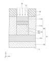
- FIG. 1 is a cross-sectional view showing the configuration of a silicon carbide semiconductor device according to a first embodiment.
- FIG. 2 is a diagram showing an example of the distribution of effective concentration of impurities.
- FIG. 3 is a cross-sectional view (part 1) showing the method for manufacturing the silicon carbide semiconductor device according to the first embodiment.
- FIG. 4 is a cross-sectional view (part 2) showing the method for manufacturing the silicon carbide semiconductor device according to the first embodiment.
- FIG. 5 is a cross-sectional view (part 3) showing the method for manufacturing the silicon carbide semiconductor device according to the first embodiment.
- FIG. 6 is a cross-sectional view (Part 4) showing the method for manufacturing the silicon carbide semiconductor device according to the first embodiment.
- FIG. 7 is a cross-sectional view (part 5) showing the method for manufacturing the silicon carbide semiconductor device according to the first embodiment.
- FIG. 8 is a cross-sectional view (part 6) showing the method for manufacturing the silicon carbide semiconductor device according to the first embodiment.
- FIG. 9 is a cross-sectional view (Part 7) showing the method for manufacturing the silicon carbide semiconductor device according to the first embodiment.
- FIG. 10 is a cross-sectional view (Part 8) showing the method for manufacturing the silicon carbide semiconductor device according to the first embodiment.
- FIG. 11 is a cross-sectional view (Part 9) showing the method for manufacturing the silicon carbide semiconductor device according to the first embodiment.
- FIG. 12 is a cross-sectional view showing a silicon carbide semiconductor device according to a second embodiment.
- FIG. 13 is a cross-sectional view showing a method for manufacturing a silicon carbide semiconductor device according to a second embodiment.
- FIG. 14 is a cross-sectional view showing a silicon carbide semiconductor device according to a third embodiment.
- FIG. 15 is a cross-sectional view (part 1) illustrating a method for manufacturing a silicon carbide semiconductor device according to a third embodiment.
- FIG. 16 is a cross-sectional view (part 2) showing the method for manufacturing the silicon carbide semiconductor device according to the third embodiment.
- An object of the present disclosure is to provide a silicon carbide semiconductor device that can reduce on-resistance and improve breakdown voltage.
- an XYZ orthogonal coordinate system is used, but the coordinate system is determined for the purpose of explanation and does not limit the posture of the silicon carbide semiconductor device or the like.
- an XY plane view is referred to as a planar view, and when viewed from an arbitrary point, the +Z direction is sometimes referred to as upward, above, or above, and the -Z direction is sometimes referred to as downward, below, or below.
- a silicon carbide semiconductor device includes a silicon carbide substrate having a first main surface and a second main surface opposite to the first main surface, and the silicon carbide substrate includes: a drift region having a first conductivity type; a body region provided on the drift region and having a second conductivity type different from the first conductivity type; and a body region provided on the body region so as to be separated from the drift region.
- a source region having the first conductivity type, and the first main surface has a side surface extending through the source region and the body region to the drift region, and a bottom surface continuous with the side surface.
- a defined gate trench is provided, and the silicon carbide substrate further includes an electric field relaxation region having the second conductivity type and provided between the gate trench and the second main surface, and the silicon carbide substrate further includes an electric field relaxation region having the second conductivity type, and The region includes a first region located between the electric field relaxation region and the first main surface, a second region adjacent to the first region in a plane parallel to the first main surface, and a second region adjacent to the first region in a plane parallel to the first main surface.
- a third region located between the region and the second main surface, connected to the second region, and adjacent to the electric field relaxation region in a plane parallel to the first main surface; a fourth region located between a third region and the second main surface and connected to the third region; a first maximum effective concentration of impurities of the first conductivity type in the first region; The value is higher than the second maximum value of the effective concentration of the first conductivity type impurity in the second region, and the third maximum value of the effective concentration of the first conductivity type impurity in the third region is higher than the third maximum value of the effective concentration of the first conductivity type impurity in the third region.
- the fourth maximum value of the effective concentration of impurities of the first conductivity type in the fourth region is not more than the third maximum value.
- the first maximum value of the effective concentration of impurities of the first conductivity type in the first region is higher than the second maximum value of the effective concentration of impurities of the first conductivity type in the second region. Therefore, while reducing the on-resistance, it is possible to suppress excessive electric field concentration below the body region and obtain a high breakdown voltage. Further, the third maximum value of the effective concentration of impurities of the first conductivity type in the third region is less than or equal to the second maximum value, and the fourth maximum value of the effective concentration of impurities of the first conductivity type in the fourth region is the third maximum value of the effective concentration of impurities of the first conductivity type in the third region. Since it is below the maximum value, an increase in electrical resistance in the second region and the third region can be suppressed. In this way, both reduction in on-resistance and improvement in breakdown voltage can be achieved.
- the third maximum value may be higher than the fourth maximum value and lower than the second maximum value. In this case, it is easy to suppress an excessive increase in electrical resistance in the second region and the third region.
- the electric field relaxation region has a first surface in contact with the first region and a second surface opposite to the first surface, and the electric field relaxation region
- the effective concentration of the second conductivity type impurity may gradually decrease from the first virtual surface 0.3 ⁇ m away from the first surface to the second surface. In this case, electric field concentration on the gate insulating film at the bottom of the gate trench can be easily alleviated.
- the first maximum value may be 50% or more of the fifth maximum value of the effective concentration of the second conductivity type impurity in the electric field relaxation region. good. In this case, it is easy to reduce the on-resistance.
- the second maximum value may be 20% or more of the fifth maximum value of the effective concentration of the second conductivity type impurity in the electric field relaxation region. good.
- the electric field in the body region on the second region tends to be higher than the electric field in the electric field relaxation region.
- the locations where electric field concentration occurs are dispersed, resulting in higher breakdown voltage.
- the thickness of the electric field relaxation region is 1 ⁇ m or more
- the electric field relaxation region has a first surface in contact with the first region
- the third The region includes a third surface that is in contact with the second region and is flush with the first surface, and a second virtual surface that is 1 ⁇ m apart from the third surface and the third surface toward the second main surface.
- a fifth region in between, and the effective concentration of impurities of the first conductivity type in the fifth region at a position separated by a first distance from the third surface toward the second main surface is:
- the effective concentration of the second conductivity type impurity in the electric field relaxation region at a position separated by the first distance from the first surface toward the second main surface may be 10% or more. In this case, depletion in the electric field relaxation region is likely to be promoted, and electric field concentration is likely to occur in the body region over the second region. Therefore, it is easy to obtain a higher withstand voltage.
- the bottom surface of the gate trench may be formed by the first region. In this case, it is easy to reduce the on-resistance.
- the width of the first region may be wider than the width of the electric field relaxation region. In this case, it is easy to reduce the on-resistance.
- the side surface of the gate trench may include a ⁇ 0-33-8 ⁇ plane. Since the side surfaces include ⁇ 0-33-8 ⁇ planes, good mobility can be obtained on the side surfaces of the gate trench, and channel resistance can be reduced.
- FIG. 1 is a cross-sectional view showing the configuration of a silicon carbide semiconductor device according to a first embodiment.
- a silicon carbide semiconductor device 100 includes a silicon carbide substrate 10, a gate insulating film 81, a gate electrode 82, an interlayer insulating film 83, a source electrode 60, and a drain. It mainly has an electrode 70.
- Silicon carbide substrate 10 has a first main surface 1 and a second main surface 2 opposite to first main surface 1 .
- the first main surface 1 and the second main surface 2 are parallel to the XY plane, and the first main surface 1 is in the +Z direction when viewed from the second main surface 2.
- Silicon carbide substrate 10 includes a silicon carbide single crystal substrate 50 and a silicon carbide epitaxial layer 40 on silicon carbide single crystal substrate 50.
- Silicon carbide epitaxial layer 40 constitutes first principal surface 1
- silicon carbide single crystal substrate 50 constitutes second principal surface 2 .
- Silicon carbide single crystal substrate 50 and silicon carbide epitaxial layer 40 are made of, for example, hexagonal silicon carbide of polytype 4H.
- Silicon carbide single crystal substrate 50 contains an n-type impurity such as nitrogen (N), and has an n-type conductivity type (first conductivity type).
- the first principal surface 1 is a ⁇ 0001 ⁇ plane or a ⁇ 0001 ⁇ plane inclined in the off direction by an off angle of 8° or less.
- the first principal surface 1 is a (000-1) plane or a plane in which the (000-1) plane is inclined in the off direction by an off angle of 8° or less.
- the off direction may be, for example, the ⁇ 11-20> direction or the ⁇ 1-100> direction.
- the off-angle may be, for example, 1° or more, or 2° or more.
- the off angle may be 6° or less, or 4° or less.
- Silicon carbide epitaxial layer 40 mainly includes drift region 11 , body region 12 , source region 13 , contact region 18 , and electric field relaxation region 16 .
- the drift region 11 contains an n-type impurity such as nitrogen or phosphorus (P), and has an n-type conductivity type.
- the drift region 11 has a first region 11A, a second region 11B, a third region 11C, and a fourth region 11D.
- Fourth region 11D is provided on silicon carbide single crystal substrate 50.
- the lower surface of fourth region 11D and the upper surface of silicon carbide single crystal substrate 50 are in contact with each other.
- the effective concentration of n-type impurities in the fourth region 11D is, for example, 1.0 ⁇ 10 15 cm ⁇ 3 or more and 5.0 ⁇ 10 16 cm ⁇ 3 or less.
- the electric field relaxation region 16 contains a p-type impurity such as aluminum (Al), and has a p-type conductivity type (second conductivity type).
- the electric field relaxation region 16 is provided on a part of the fourth region 11D.
- the lower surface of the electric field relaxation region 16 and the upper surface of the fourth region 11D are in contact with each other.
- the effective concentration of p-type impurities in the electric field relaxation region 16 is, for example, 1.0 ⁇ 10 16 cm ⁇ 3 or more and 5.0 ⁇ 10 18 cm ⁇ 3 or less.
- the lower surface of the electric field relaxation region 16 may be separated from the upper surface of the fourth region 11D, and a portion of the third region 11C may exist between them.
- the lower surface of the electric field relaxation region 16 and the lower surface of the third region 11C may not be flush with each other, and the lower surface of the electric field relaxation region 16 may be closer to the second main surface 2 than the lower surface of the third region 11C. That is, the electric field relaxation region 16 may be formed deeper than the third region 11C.
- the third region 11C is provided on a part of the fourth region 11D.
- the lower surface of the third region 11C and the upper surface of the fourth region 11D are in contact with each other.
- the third region 11C is adjacent to the electric field relaxation region 16.
- the side surface of the third region 11C and the side surface of the electric field relaxation region 16 are in contact with each other.
- the effective concentration of n-type impurities in the third region 11C is, for example, 5.0 ⁇ 10 15 cm ⁇ 3 or more and 2.0 ⁇ 10 18 cm ⁇ 3 or less.
- the first region 11A is provided on the electric field relaxation region 16.
- the lower surface of the first region 11A and the upper surface of the electric field relaxation region 16 are in contact with each other.
- the effective concentration of n-type impurities in the first region 11A is, for example, 1.0 ⁇ 10 16 cm ⁇ 3 or more and 2.0 ⁇ 10 18 cm ⁇ 3 or less.
- the second region 11B is provided on the third region 11C.
- the lower surface of the second region 11B and the upper surface of the third region 11C are in contact with each other.
- the second region 11B is adjacent to the first region 11A.
- the side surface of the second region 11B and the side surface of the first region 11A are in contact with each other.
- the effective concentration of n-type impurities in the second region 11B is, for example, 1.0 ⁇ 10 16 cm ⁇ 3 or more and 1.0 ⁇ 10 18 cm ⁇ 3 or less.
- the first region 11A and the second region 11B are sometimes called current diffusion regions.
- the interface between the third region 11C and the second region 11B is flush with the interface between the electric field relaxation region 16 and the first region 11A.
- the interface between the third region 11C and the second region 11B may be closer to the first main surface 1 or the second main surface 2 than the interface between the electric field relaxation region 16 and the first region 11A.
- the interface between the first region 11A and the second region 11B may be flush with the interface between the electric field relaxation region 16 and the third region 11C, or may be located above the third region 11C. That is, the width of the first region 11A may be equal to the width of the electric field relaxation region 16, or may be wider than the width of the electric field relaxation region 16.
- the first region 11A is located between the electric field relaxation region 16 and the first main surface 1.
- the second region 11B is adjacent to the first region 11A in a plane parallel to the first main surface 1.
- the third region 11C is located between the second region 11B and the second main surface 2, is connected to the second region 11B, and is adjacent to the electric field relaxation region 16 in a plane parallel to the first main surface 1.
- the fourth region 11D is located between the electric field relaxation region 16 and the third region 11C and the second main surface 2, and is connected to the third region 11C.
- Body region 12 contains, for example, a p-type impurity such as aluminum, and has p-type conductivity type. Body region 12 is provided above drift region 11 . The body region 12 is provided on the first region 11A and the second region 11B. The effective concentration of p-type impurities in the body region 12 is, for example, 1.0 ⁇ 10 17 cm ⁇ 3 or more and 5.0 ⁇ 10 18 cm ⁇ 3 or less.
- Source region 13 contains an n-type impurity such as nitrogen or phosphorus, and has n-type conductivity. Source region 13 is provided above body region 12 . Source region 13 is separated from drift region 11 by body region 12 . Source region 13 constitutes first main surface 1 .
- the effective concentration of n-type impurities in the source region 13 is, for example, 5.0 ⁇ 10 18 cm ⁇ 3 or more and 2.0 ⁇ 10 20 cm ⁇ 3 or less.
- Contact region 18 contains, for example, a p-type impurity such as aluminum, and has p-type conductivity type. Contact region 18 penetrates source region 13 and contacts body region 12 . Contact region 18 constitutes first main surface 1 .
- the effective p-type impurity concentration of the contact region 18 is, for example, 1.0 ⁇ 10 18 cm ⁇ 3 or more and 5.0 ⁇ 10 20 cm ⁇ 3 or less.
- Electric field relaxation region 16 is electrically connected to contact region 18 . Note that the contact region 18 may be formed at a position that appears in a cross section different from the cross section shown in FIG.
- a gate trench 5 defined by a side surface 3 and a bottom surface 4 is provided on the first main surface 1 .
- Gate trench 5 extends, for example, along the Y axis.
- Side surface 3 penetrates source region 13, body region 12, and part of first region 11A, and reaches first region 11A.
- the bottom surface 4 is continuous with the side surface 3.
- the bottom surface 4 is located in the first region 11A.
- the bottom surface 4 is parallel to the first main surface 1 and the second main surface 2.
- the angle ⁇ 1 of the side surface 3 with respect to the plane including the bottom surface 4 is, for example, 45° or more and 65° or less.
- the angle ⁇ 1 may be, for example, 50° or more.
- the angle ⁇ 1 may be, for example, 60° or less.
- the side surface 3 preferably has a ⁇ 0-33-8 ⁇ plane.
- the ⁇ 0-33-8 ⁇ plane is a crystal plane that provides excellent mobility.
- the gate insulating film 81 is, for example, an oxide film.
- the gate insulating film 81 is made of a material containing silicon dioxide, for example.
- the gate insulating film 81 is in contact with the side surfaces 3 and the bottom surface 4 .
- the gate insulating film 81 is in contact with the first region 11A at the bottom surface 4.
- Gate insulating film 81 contacts source region 13, body region 12, and first region 11A on side surface 3.
- Gate insulating film 81 may be in contact with source region 13 on first main surface 1 .
- the gate electrode 82 is provided on the gate insulating film 81.
- the gate electrode 82 is made of, for example, polysilicon (polySi) containing conductive impurities. Gate electrode 82 is placed inside gate trench 5 . A portion of the gate electrode 82 may be placed on the first main surface 1.
- the interlayer insulating film 83 covers the gate electrode 82. Interlayer insulating film 83 is in contact with gate electrode 82 and gate insulating film 81 .
- the interlayer insulating film 83 is, for example, an oxide film.
- the interlayer insulating film 83 is made of a material containing silicon dioxide, for example. Interlayer insulating film 83 electrically insulates gate electrode 82 and source electrode 60 from each other. A portion of interlayer insulating film 83 may be provided inside gate trench 5 .
- a barrier metal film 84 is provided to cover the top and side surfaces of the interlayer insulating film 83 and the side surfaces of the gate insulating film 81.
- Barrier metal film 84 is in contact with interlayer insulating film 83 and gate insulating film 81 .
- the barrier metal film 84 is made of a material containing, for example, titanium nitride (TiN).
- a contact hole 90 is formed in the interlayer insulating film 83 and the gate insulating film 81. Source region 13 is exposed from interlayer insulating film 83 and gate insulating film 81 through contact hole 90 .
- the source electrode 60 is in contact with the first main surface 1.
- the source electrode 60 has a contact electrode 61 provided in the contact hole 90 and a source wiring 62.
- Contact electrode 61 is in contact with source region 13 and contact region 18 on first main surface 1 .
- the contact electrode 61 is made of a material containing, for example, nickel silicide (NiSi).
- the contact electrode 61 may be made of a material containing titanium (Ti), aluminum, and silicon.
- Contact electrode 61 is in ohmic contact with source region 13 and contact region 18 .
- the source wiring 62 covers the upper surface and side surfaces of the interlayer insulating film 83 and the upper surface of the contact electrode 61.
- the source wiring 62 is in contact with the barrier metal film 84 and the contact electrode 61.
- the source wiring 62 is made of a material containing aluminum, for example.
- a potential is applied to body region 12 and electric field relaxation region 16 from source electrode 60 via contact region 18 .
- the drain electrode 70 is in contact with the second main surface 2. Drain electrode 70 is in contact with silicon carbide single crystal substrate 50 at second main surface 2 . Drain electrode 70 is electrically connected to drift region 11 .
- the drain electrode 70 is made of a material containing, for example, nickel silicide.
- the drain electrode 70 may be made of a material containing titanium, aluminum, and silicon. Drain electrode 70 is in ohmic contact with silicon carbide single crystal substrate 50 .
- a buffer layer containing an n-type impurity such as nitrogen and having n-type conductivity may be provided between silicon carbide single crystal substrate 50 and fourth region 11D.
- the effective concentration of n-type impurities in the buffer layer may be higher than the effective concentration of n-type impurities in the fourth region 11D.
- the effective concentration of p-type impurities in a p-type region is a value obtained by subtracting the concentration of n-type impurities from the concentration of p-type impurities in the region.
- the effective concentration of n-type impurities in an n-type region is a value obtained by subtracting the concentration of p-type impurities from the concentration of n-type impurities in the region.
- the effective concentration of p-type impurities and the effective concentration of n-type impurities can be measured, for example, by a scanning capacitance microscope (SCM) method or a secondary ion mass spectrometry (SIMS) method. be.
- SCM scanning capacitance microscope
- SIMS secondary ion mass spectrometry
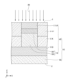
- FIG. 2 is a diagram showing an example of the distribution of effective concentration of impurities.
- FIG. 2 shows the distribution of the absolute value of the effective concentration of impurities along the two-dot chain line L in FIG.
- the horizontal axis in FIG. 2 indicates the depth with respect to the first main surface 1, and the vertical axis indicates the absolute value of the effective concentration of impurities.
- the first maximum value of the effective concentration of n-type impurities in the first region 11A is higher than the second maximum value of the effective concentration of n-type impurities in the second region 11B.
- the third maximum value of the effective concentration of n-type impurities in the third region 11C is less than or equal to the second maximum value.
- the fourth maximum value of the effective concentration of n-type impurities in the fourth region 11D is equal to or less than the third maximum value.
- the maximum effective concentration of n-type impurities in source region 13 may be higher than the maximum effective concentration of p-type impurities in body region 12.
- the maximum value of the effective concentration of p-type impurities in body region 12 may be higher than the first maximum value of the effective concentration of n-type impurities in first region 11A.
- the first maximum value of the effective concentration of n-type impurities in the first region 11A may be higher than the fifth maximum value of the effective concentration of p-type impurities in the electric field relaxation region 16.
- 3 to 11 are cross-sectional views showing a method of manufacturing a silicon carbide semiconductor device according to the first embodiment.
- silicon carbide single crystal substrate 50 is prepared.
- silicon carbide epitaxial layer 40 is formed on silicon carbide single crystal substrate 50 .
- Silicon carbide epitaxial layer 40 includes a fourth region 11D and an n-type region 111C in which a third region 11C and the like will be formed later.
- silicon carbide single crystal substrate 50 contains n-type impurities such as nitrogen and has n-type conductivity type.
- silicon carbide epitaxial layer 40 can be formed by epitaxial growth doped with n-type impurities such as nitrogen. In this way, silicon carbide substrate 10 having first main surface 1 and second main surface 2 is obtained.
- a resist mask 30 is formed on the silicon carbide epitaxial layer 40.
- An opening 31 is formed in the resist mask 30 to expose a region where the electric field relaxation region 16 of the n-type region 111C is to be formed.
- p-type impurity 21 is ion-implanted through opening 31 to form p-type region 116 in n-type region 111C.
- the p-type region 116 is a region that becomes the electric field relaxation region 16, and is formed to a shallower region than the electric field relaxation region 16.
- channeling implantation is performed, for example. That is, ion implantation is performed perpendicularly to the ⁇ 0001 ⁇ plane.
- an n-type impurity 22 is ion-implanted through the opening 31 to form an n-type region 111A within the n-type region 111C.
- the n-type region 111A is a region that becomes the first region 11A, but is formed to a shallower region than the first region 11A.
- the n-type region 111A constitutes the first main surface 1.
- the n-type region 111A is formed so as to partially overlap the p-type region 116.
- electric field relaxation region 16 is formed from p-type region 116.
- ions are implanted perpendicularly to the first main surface 1 along the Z axis.
- the resist mask 30 is removed and p-type impurity 23 is ion-implanted into the entire first main surface 1, thereby forming p-type regions in the n-type regions 111C and 111A. 112 is formed.
- the p-type region 112 is a region that will become the body region 12, it is formed to a shallower region than the body region 12.
- p-type region 112 constitutes first main surface 1 .
- ions are implanted perpendicularly to the first main surface 1 along the Z axis.
- an n-type impurity 24 is ion-implanted into the entire first main surface 1 to form an n-type region 113 in the p-type region 112, and an n-type region 111A
- a first region 11A is formed within the n-type region 111C
- a second region 11B is formed within the n-type region 111C.
- a third region 11C is formed from the n-type region 111C.
- the ion implantation is performed perpendicularly to the first main surface 1 along the Z axis.
- a contact region is formed in the n-type region 113 by implanting p-type impurity ions into a part of the first main surface 1 using a resist mask (not shown). form 18.
- source region 13 is formed from n-type region 113.
- ions are implanted perpendicularly to the first main surface 1 along the Z axis.
- a gate trench 5 having side surfaces 3 and a bottom surface 4 is formed.
- the gate trench 5 can be formed by, for example, reactive ion etching (RIE), thermal etching, etc. using a mask.
- RIE reactive ion etching
- a gate insulating film 81, a gate electrode 82, and an interlayer insulating film 83 are formed.
- a contact hole 90 is formed in the gate insulating film 81 and the interlayer insulating film 83, and a barrier metal film 84 is formed.
- a source electrode 60 including a contact electrode 61 and a source wiring 62 is formed. Additionally, a drain electrode 70 is formed.
- silicon carbide semiconductor device 100 according to the first embodiment can be manufactured.
- the first maximum value of the effective concentration of n-type impurities in first region 11A is higher than the second maximum value of the effective concentration of n-type impurities in second region 11B. . Therefore, while reducing the on-resistance, it is possible to suppress excessive electric field concentration below the body region 12 and obtain a high breakdown voltage. Further, since the second maximum value is smaller than the first maximum value, the capacitance between the source electrode 60 and the drain electrode 70 can be kept low, and switching loss can be reduced.
- the third maximum value of the effective concentration of n-type impurities in the third region 11C is equal to or less than the second maximum value. Therefore, an increase in electrical resistance in the second region 11B can be suppressed.
- the third maximum value is higher than the fourth maximum value.
- the fourth maximum value of the effective concentration of n-type impurities in the fourth region 11D is equal to or less than the third maximum value. Therefore, an increase in electrical resistance in the third region 11C can be suppressed. For example, even if the electric field relaxation regions 16 and the third regions 11C are arranged alternately and a plurality of cells are arranged, the electrical resistance in the third region 11C between the adjacent electric field relaxation regions 16 can be suppressed to a low level.
- the third maximum value is lower than the second maximum value.
- the electric field relaxation region 16 has a first surface 41 in contact with the first region 11A, and a second surface 42 opposite to the first surface 41.
- the effective concentration of p-type impurities in the electric field relaxation region 16 is from the first virtual surface 51 to the second surface 42, which is 0.3 ⁇ m apart from the first surface 41 toward the second surface 42. It gradually decreases over time. In this case, electric field concentration on the gate insulating film 81 at the bottom of the gate trench 5 can be easily alleviated.
- the first maximum value is preferably 50% or more of the fifth maximum value of the effective concentration of p-type impurities in the electric field relaxation region 16. In this case, it is easy to reduce the on-resistance.
- the first maximum value is preferably 60% or more, and even more preferably 70% or more, of the fifth maximum value. Note that, in order to suppress punch-through in the portion of the body region 12 that functions as a channel, the first maximum value is preferably lower than the maximum value of the effective concentration of p-type impurities in the body region 12.
- the second maximum value is preferably 20% or more of the fifth maximum value of the effective concentration of p-type impurities in the electric field relaxation region 16.
- the electric field in the body region 12 tends to be higher than the electric field in the electric field relaxation region 16 on the second region 11B.
- the locations where electric field concentration occurs are dispersed, resulting in higher breakdown voltage.
- the second maximum value is preferably 30% or more, and even more preferably 40% or more, of the fifth maximum value.
- the third region 11C has a third surface 43 that is flush with the first surface 41.
- the third surface 43 contacts the second region 11B.
- the third region 11C further includes a fifth region 11E.
- the fifth region 11E is a region between the third surface 43 and the second virtual surface 52 that is 1 ⁇ m away from the third surface 43 toward the second main surface 2.
- the thickness of the electric field relaxation region 16 is 1 ⁇ m or more, and the effective concentration of n-type impurities in the fifth region 11E at a position away from the third surface 43 by the first distance toward the second main surface 2 is the first It is preferably 10% or more, more preferably 20% or more of the effective concentration of the p-type impurity in the electric field relaxation region 16 at a position separated by the first distance from the surface 41 toward the second main surface 2, More preferably, it is 30% or more. When such a relationship holds true, depletion within the electric field relaxation region 16 is likely to be promoted. Further, electric field concentration tends to occur in the body region 12 on the second region 11B. Therefore, higher breakdown voltage can be obtained.
- the thickness of the electric field relaxation region 16 is preferably 1 ⁇ m or more, more preferably 1.5 ⁇ m or more, and still more preferably 2 ⁇ m or more.
- the bottom surface 4 of the gate trench 5 is constituted by the first region 11A, it is easy to reduce the on-resistance. Further, when the width of the first region 11A is wider than the width of the electric field relaxation region 16, it is easier to reduce the on-resistance.
- FIG. 12 is a cross-sectional view showing a silicon carbide semiconductor device according to a second embodiment.
- electric field relaxation region 16 includes sixth region 16X and seventh region 16Y.
- the sixth region 16X is provided on a part of the fourth region 11D.
- the lower surface of the sixth region 16X and the upper surface of the fourth region 11D are in contact with each other.
- the seventh region 16Y is provided on the sixth region 16X.
- the lower surface of the seventh region 16Y and the upper surface of the sixth region 16X are in contact with each other.
- the upper surface of the seventh region 16Y and the lower surface of the first region 11A are in contact with each other.
- the effective concentration of p-type impurities in the seventh region 16Y is higher than the effective concentration of p-type impurities in the sixth region 16X.
- the effective concentration of p-type impurities in the sixth region 16X is, for example, 1.0 ⁇ 10 16 cm ⁇ 3 or more and 4.0 ⁇ 10 18 cm ⁇ 3 or less.
- the effective concentration of p-type impurities in the seventh region 16Y is, for example, 1.0 ⁇ 10 17 cm ⁇ 3 or more and 5.0 ⁇ 10 18 cm ⁇ 3 or less.
- FIG. 13 is a cross-sectional view showing a method for manufacturing a silicon carbide semiconductor device according to a second embodiment.
- processing up to ion implantation of the n-type impurity 22 is performed (see FIG. 6).
- the electric field relaxation region 16 is not formed at the time when the n-type region 111A is formed.
- the p-type impurity 25 is ion-implanted through the opening 31 to form a seventh region 16Y in the p-type region 116.
- a sixth region 16X is formed from the p-type region 116.
- an electric field relaxation region 16 having a sixth region 16X and a seventh region 16Y is formed.
- the ion implantation is performed perpendicularly to the first main surface 1 along the Z axis.
- silicon carbide semiconductor device 200 according to the second embodiment can be manufactured.
- the second embodiment also provides the same effects as the first embodiment.
- FIG. 14 is a cross-sectional view showing a silicon carbide semiconductor device according to a third embodiment.
- third region 11C includes eighth region 11X and ninth region 11Y.
- the eighth region 11X is provided on a part of the fourth region 11D.
- the lower surface of the eighth region 11X and the upper surface of the fourth region 11D are in contact with each other.
- the ninth region 11Y is provided on the eighth region 11X.
- the lower surface of the ninth region 11Y and the upper surface of the eighth region 11X are in contact with each other.
- the upper surface of the ninth region 11Y and the lower surface of the second region 11B are in contact with each other.
- the effective concentration of n-type impurities in the ninth region 11Y is higher than the effective concentration of p-type impurities in the eighth region 11X.
- the effective concentration of n-type impurities in the eighth region 11X is, for example, 5.0 ⁇ 10 15 cm ⁇ 3 or more and 5.0 ⁇ 10 17 cm ⁇ 3 or less.
- the effective concentration of n-type impurities in the ninth region 11Y is, for example, 1.0 ⁇ 10 16 cm ⁇ 3 or more and 1.0 ⁇ 10 18 cm ⁇ 3 or less.
- the interface between the eighth region 11X and the ninth region 11Y may coincide with the second virtual surface 52 (see FIG. 1), and may be closer to the first principal surface 1 than the second virtual surface 52. , may be closer to the second principal surface 2 than the second virtual surface 52.
- the second virtual surface 52 is a surface that is 1 ⁇ m away from the third surface 43 in contact with the second region 11B toward the second main surface 2.
- FIG. 15 and FIG. 15 are cross-sectional views showing a method for manufacturing a silicon carbide semiconductor device according to a third embodiment.
- an n-type impurity 26 is ion-implanted into the entire first main surface 1 to form an n-type region 111Y in the n-type region 111C.
- the n-type region 111Y is a region that will become the ninth region 11Y, and is formed to a shallower region than the ninth region 11Y.
- the n-type region 111Y constitutes the first main surface 1.
- eighth region 11X is formed from n-type region 111C.
- channeling implantation is performed, for example. That is, ion implantation is performed perpendicularly to the ⁇ 0001 ⁇ plane.
- the second region 11B is formed by ion implantation of the n-type impurity 24 into the entire first main surface 1 (see FIG. 8), and with the formation of the second region 11B, the ninth region 11Y is expanded from the n-type region 111X. (See FIG. 14). As a result, a third region 11C having an eighth region 11X and a ninth region 11Y is formed. In this way, silicon carbide semiconductor device 300 according to the third embodiment can be manufactured.
- the third embodiment also provides the same effects as the first and second embodiments.
- a hard mask such as polysilicon or silicon oxide may be used instead of a resist mask.
Landscapes
- Electrodes Of Semiconductors (AREA)
Priority Applications (3)
| Application Number | Priority Date | Filing Date | Title |
|---|---|---|---|
| CN202380032110.3A CN118974943A (zh) | 2022-05-25 | 2023-01-25 | 碳化硅半导体器件 |
| DE112023002435.9T DE112023002435T5 (de) | 2022-05-25 | 2023-01-25 | Siliziumkarbid-Halbleitervorrichtung |
| JP2024522905A JPWO2023228473A1 (https=) | 2022-05-25 | 2023-01-25 |
Applications Claiming Priority (2)
| Application Number | Priority Date | Filing Date | Title |
|---|---|---|---|
| JP2022-085313 | 2022-05-25 | ||
| JP2022085313 | 2022-05-25 |
Publications (1)
| Publication Number | Publication Date |
|---|---|
| WO2023228473A1 true WO2023228473A1 (ja) | 2023-11-30 |
Family
ID=88918893
Family Applications (1)
| Application Number | Title | Priority Date | Filing Date |
|---|---|---|---|
| PCT/JP2023/002283 Ceased WO2023228473A1 (ja) | 2022-05-25 | 2023-01-25 | 炭化珪素半導体装置 |
Country Status (4)
| Country | Link |
|---|---|
| JP (1) | JPWO2023228473A1 (https=) |
| CN (1) | CN118974943A (https=) |
| DE (1) | DE112023002435T5 (https=) |
| WO (1) | WO2023228473A1 (https=) |
Citations (4)
| Publication number | Priority date | Publication date | Assignee | Title |
|---|---|---|---|---|
| WO2019155783A1 (ja) * | 2018-02-06 | 2019-08-15 | 住友電気工業株式会社 | 炭化珪素半導体装置 |
| WO2020031446A1 (ja) * | 2018-08-09 | 2020-02-13 | 住友電気工業株式会社 | 炭化珪素半導体装置および炭化珪素半導体装置の製造方法 |
| JP2020136416A (ja) * | 2019-02-15 | 2020-08-31 | 富士電機株式会社 | 半導体装置および半導体装置の製造方法 |
| JP2021184412A (ja) * | 2020-05-21 | 2021-12-02 | 株式会社東芝 | 半導体装置 |
Family Cites Families (3)
| Publication number | Priority date | Publication date | Assignee | Title |
|---|---|---|---|---|
| JP5985662B2 (ja) | 2013-01-23 | 2016-09-06 | 株式会社日立製作所 | 炭化珪素半導体装置及びその製造方法 |
| JP6453188B2 (ja) | 2015-09-04 | 2019-01-16 | 株式会社豊田中央研究所 | 炭化珪素半導体装置 |
| JP7188790B2 (ja) | 2020-11-27 | 2022-12-13 | Necプラットフォームズ株式会社 | 情報処理装置、無線通信システム、算出方法及びプログラム |
-
2023
- 2023-01-25 CN CN202380032110.3A patent/CN118974943A/zh active Pending
- 2023-01-25 JP JP2024522905A patent/JPWO2023228473A1/ja active Pending
- 2023-01-25 WO PCT/JP2023/002283 patent/WO2023228473A1/ja not_active Ceased
- 2023-01-25 DE DE112023002435.9T patent/DE112023002435T5/de active Pending
Patent Citations (4)
| Publication number | Priority date | Publication date | Assignee | Title |
|---|---|---|---|---|
| WO2019155783A1 (ja) * | 2018-02-06 | 2019-08-15 | 住友電気工業株式会社 | 炭化珪素半導体装置 |
| WO2020031446A1 (ja) * | 2018-08-09 | 2020-02-13 | 住友電気工業株式会社 | 炭化珪素半導体装置および炭化珪素半導体装置の製造方法 |
| JP2020136416A (ja) * | 2019-02-15 | 2020-08-31 | 富士電機株式会社 | 半導体装置および半導体装置の製造方法 |
| JP2021184412A (ja) * | 2020-05-21 | 2021-12-02 | 株式会社東芝 | 半導体装置 |
Also Published As
| Publication number | Publication date |
|---|---|
| DE112023002435T5 (de) | 2025-03-20 |
| CN118974943A (zh) | 2024-11-15 |
| JPWO2023228473A1 (https=) | 2023-11-30 |
Similar Documents
| Publication | Publication Date | Title |
|---|---|---|
| US12295156B2 (en) | Semiconductor device including trench gate structure and buried shielding region and method of manufacturing | |
| US10002952B2 (en) | Silicon carbide semiconductor device and method of manufacturing silicon carbide semiconductor device | |
| US9825166B2 (en) | Silicon carbide semiconductor device and method for producing same | |
| JP6168732B2 (ja) | 炭化珪素半導体装置およびその製造方法 | |
| JP5586887B2 (ja) | 半導体装置及びその製造方法 | |
| CN102770960B (zh) | 半导体器件及其制造方法 | |
| US8536641B1 (en) | Semiconductor device | |
| US20260006810A1 (en) | Silicon carbide device with a trench gate structure and a shielding region | |
| JP6532549B2 (ja) | 半導体装置 | |
| US20080153216A1 (en) | Method for manufacturing silicon carbide semiconductor device | |
| US10777678B2 (en) | Semiconductor device | |
| US20110140197A1 (en) | Semiconductor device and method for manufacturing the same | |
| US12279448B2 (en) | Trench bottom shielding methods and approaches for trenched semiconductor device structures | |
| CN111081779A (zh) | 一种屏蔽栅沟槽式mosfet及其制造方法 | |
| US10418478B2 (en) | Semiconductor device | |
| US11769828B2 (en) | Gate trench power semiconductor devices having improved deep shield connection patterns | |
| WO2023228473A1 (ja) | 炭化珪素半導体装置 | |
| WO2022270245A1 (ja) | 炭化珪素半導体装置 | |
| JP2023104657A (ja) | 炭化珪素半導体装置 | |
| JP2018046139A (ja) | 半導体装置、および、半導体装置の製造方法 | |
| US20250212473A1 (en) | Nitride semiconductor device and method of manufacturing the same | |
| US20250324740A1 (en) | Semiconductor device and method for manufacturing the same | |
| WO2025127078A1 (ja) | 炭化珪素半導体装置 | |
| JP7124582B2 (ja) | 炭化珪素半導体装置 | |
| JP2024095141A (ja) | 炭化珪素半導体装置 |
Legal Events
| Date | Code | Title | Description |
|---|---|---|---|
| 121 | Ep: the epo has been informed by wipo that ep was designated in this application |
Ref document number: 23811354 Country of ref document: EP Kind code of ref document: A1 |
|
| WWE | Wipo information: entry into national phase |
Ref document number: 202380032110.3 Country of ref document: CN |
|
| WWE | Wipo information: entry into national phase |
Ref document number: 2024522905 Country of ref document: JP |
|
| WWE | Wipo information: entry into national phase |
Ref document number: 112023002435 Country of ref document: DE |
|
| WWP | Wipo information: published in national office |
Ref document number: 112023002435 Country of ref document: DE |
|
| 122 | Ep: pct application non-entry in european phase |
Ref document number: 23811354 Country of ref document: EP Kind code of ref document: A1 |